
 Open Access Article
 This Open Access Article is licensed under a
 Creative Commons Attribution 3.0 Unported Licence
Energy augmentation of triboelectric nanogenerators using PDMS–MWCNT composites and their applications in IoT and HMI sensing†
Shailendra
Kumar
*a,
Tarun Pratap
Singh
b,
Rajesh Kumar
Jha
 a,
Prashant
Sharma
a,
Sumit
Sinha-Ray
c and
Ankur
Goswami
*a
a,
Prashant
Sharma
a,
Sumit
Sinha-Ray
c and
Ankur
Goswami
*a
aDepartment of Materials Science and Engineering, Indian Institute of Technology Delhi, Hauz Khas, New Delhi-110016, India. E-mail: msz198714@mse.iitd.ac.in; agoswami@mse.iitd.ac.in
bSchool of Interdisciplinary Research, Indian Institute of Technology Delhi, Hauz Khas, New Delhi-110016, India
cDepartment of Textile and Fibre Engineering, Indian Institute of Technology Delhi, Hauz Khas, New Delhi-110016, India
First published on 7th May 2025
Abstract
Triboelectric nanogenerators (TENGs) have become viable self-powered systems, with great potential to satisfy the increasing demand for portable and adaptable power sources. Using these systems, mechanical vibrations from the motion of vehicles, human beings, rain falls, ocean waves, and air flows can be efficiently captured Depending on the triboelectric series, various materials have been used and explored for TENG applications. In this work, we investigated the triboelectric characteristics of spin-coated polydimethylsiloxane (PDMS) and multiwall carbon nanotube (MWCNT) composite membranes. By adding various concentrations of MWCNTs in PDMS, the charge transfer efficiency was investigated in terms of the current output. At the optimized composition of 0.05 wt% MWCNTs in PDMS, an open-circuit voltage (Voc) of 110 V and a short-circuit current (Isc) of 10 μA were observed leading to a power density of nearly 1 W m−2. Additionally, this composition demonstrated outstanding long-term durability and electrical stability, facilitating energy harvesting during routine activities like jogging and walking using clothing and shoes.
 Shailendra Kumar | Shailendra Kumar is currently a PhD Scholar in the Department of Materials Science and Engineering at Indian Institute of Technology Delhi. He obtained his MTech degree in Advanced Materials Science and Technology from the National Institute of Technology, Durgapur, West Bengal, India, in 2019. His research interests include triboelectric nanogenerators, energy harvesting, thin films, and 2D materials. |
 Tarun Pratap Singh | Tarun Pratap Singh earned his BTech degree from the National Institute of Technology (NIT), Uttarakhand, in 2017 and completed his MTech degree at Indian Institute of Technology (IIT) Mandi in 2020. Since 2023, he has been pursuing his PhD degree at Indian Institute of Technology (IIT) Delhi, India. His research interests include triboelectric nanogenerators and fabrication of nano- and micro-fibers using techniques such as electrospinning, solution-blowing, and supersonic-blowing processes. |
 Rajesh Kumar Jha | Dr Rajesh Kumar Jha is an Institute Postdoc Fellow in the Department of Materials Science and Engineering at Indian Institute of Technology Delhi. He obtained his PhD degree in Electronics and Communication Engineering from IIIT Allahabad in 2020. His research interests include VLSI, semiconductor devices and triboelectric nanogenerators. |
 Prashant Sharma | Prashant Sharma earned his BS-MS dual degree in Mathematics and Physics from the Indian Institute of Science Education and Research, Thiruvananthapuram, in 2024. Currently, he is pursuing his research as a Project Student in the Department of Materials Science and Engineering at Indian Institute of Technology Delhi. His research interests lie at the intersection of sensor integration, instrumentation, and embedded electronics, with a particular focus on neural network-based classification techniques. |
 Sumit Sinha-Ray | Prof. Sumit Sinha Ray is serving as an Assistant Professor at the Department of Textile and Fibre Engineering, IIT Delhi. His research interests include heat-mass transfer phenomena and energy conversion/storage using nanoarchitectures from polymeric materials. |
 Ankur Goswami | Prof. Ankur Goswami is currently an Assistant Professor in the Department of Materials Science and Engineering at IIT Delhi, India. His current research interests include the fabrication of MEMS devices, novel energy-harvesting devices, electronic and optical switches using smart materials and the use of scanning probe microscopy to investigate the electronic properties of materials at the surface. |
1. Introduction
As an alternate way for powering portable gadgets, healthcare equipment, and wireless sensor systems, energy-harvesting technologies have attracted significant attention in recent years.1,2 Extensive studies have been devoted to the field of wearable devices to harness energy from human motion.3–6 In particular, recent years have seen a surge in the research on the use of triboelectric nanogenerators (TENGs) to convert the motions of the human body into electric energy for use in power portable devices, internet of things (IoT) gadgets and water proof textiles.7 TENGs are flexible, efficient, and cost-effective energy harvesters.8,9 One of the most significant obstacles that must be overcome to produce flexible energy-harvesting devices is the selection of suitable materials that can provide both flexibility and mechanical stability.10–12 Additionally, the design and construction of the whole structure must be accomplished. Significant efforts have been devoted to improve the performance of flexible TENGs over the last decade, with the intention of broadening their applications. Polydimethylsiloxane (PDMS) is recognized as one of the most durable organic, nonmetallic, and flexible materials. This makes it highly suitable for use as a triboelectric material, typically classified within the series of tribo-negative materials. It features great flexibility, stretchability, and biocompatibility, which are necessary for wearable energy harvesters.12,13 Furthermore, PDMS possesses very high dielectric constant characteristics, which allow it to simultaneously absorb and store the electrostatic charges that are formed during the triboelectric process. This generation of the charge because of their difference in electronegativity is referred to as the triboelectric process, which arises from the difference in electronegativity between contacting materials. It has been shown in several studies that the energy-conversion capabilities of these devices can be enhanced via surface modification through the process of nano-structuring, which typically involves increasing the surface area of the parent matrix of the TENGs. There have been many studies that have demonstrated an increase in the energy-conversion efficiency of PDMS-based TENGs, using several types of conductive materials.14,15 Multiwall carbon nanotubes, also known as MWCNTs, are one of the most effective materials for improving the electrical characteristics of materials. The atomic structure of MWCNTs is one of a kind, and as a result, they boast outstanding mechanical strength, electrochemical stability, electrical conductivity, and thermal resistance.16–18 As a result of the incorporation of MWCNTs into PDMS, the surface charge density and ability to transfer charge can be significantly boosted, which ultimately results in enhanced performance across a variety of applications. Within the context of PDMS-based materials, this combination makes use of the remarkable properties of MWCNTs to improve the overall functioning and longevity of products.MWCNTs have emerged as potential conductive materials for improving the performance output of triboelectric nanogenerators (TENGs). Recently, Salauddin et al. proposed a TENG utilizing MXene-integrated eco-flex composites encased in fabric, with MXene functioning as the tribo-negative layer. The device attained a maximum output power of 3.69 mW at an input impedance of 4.5 MΩ, with an applied force of 8 N and a frequency of 4.5 Hz.19 In a similar way, Yang et al. engineered a flexible hybrid nanogenerator that integrated piezoelectric and triboelectric elements in an Al/PVDF/Cu-PDMS/ITO/PET configuration, achieving a peak current of 20 μA, voltage of 88 V, and power output of 98 μW.20 Zhu et al. examined PDMS-Ag nanocomposites, yielding an output voltage of 33.6 V, current of 4.5 μA, and power density of 162 mW m−2 at a pressure of 53.57 kPa.21 In a separate investigation, Hajra et al. presented a ZIF-67-based TENG for autonomous robotic object identification, attaining a peak output voltage of 118 V, short-circuit current of 1.7 μA, and power density of 0.15 W m−2.22
The innovation in the present work is the creation of a high-performance, flexible TENG utilizing a PDMS–MWCNT composite membrane, optimized by meticulous regulation of the MWCNT composition. The incorporation of 0.050 wt% MWCNTs into the PDMS matrix significantly enhanced the triboelectric performance of the TENG, resulting in a power density of 0.97 W m−2, output voltage of 110 V, and current of 10 μA, while also demonstrating exceptional durability over 10![[thin space (1/6-em)]](https://www.rsc.org/images/entities/char_2009.gif) 000 operating cycles. The effective incorporation of the TENG into wearable devices for energy harvesting from human motion was demonstrated, underscoring its potential for practical use in self-powered sensing technologies. This scalable manufacturing approach distinguishes itself from prior research by providing a dependable, robust, and efficient solution for wearable energy harvesting. Additionally, to replicate authentic motion events, we created and evaluated a wearable prototype.
000 operating cycles. The effective incorporation of the TENG into wearable devices for energy harvesting from human motion was demonstrated, underscoring its potential for practical use in self-powered sensing technologies. This scalable manufacturing approach distinguishes itself from prior research by providing a dependable, robust, and efficient solution for wearable energy harvesting. Additionally, to replicate authentic motion events, we created and evaluated a wearable prototype.
2. Results and discussion
2.1. Optimization and characterization of TENG
![[double bond, length as m-dash]](https://www.rsc.org/images/entities/char_e001.gif) C bonds or the elongation of aromatic rings.27
C bonds or the elongation of aromatic rings.27
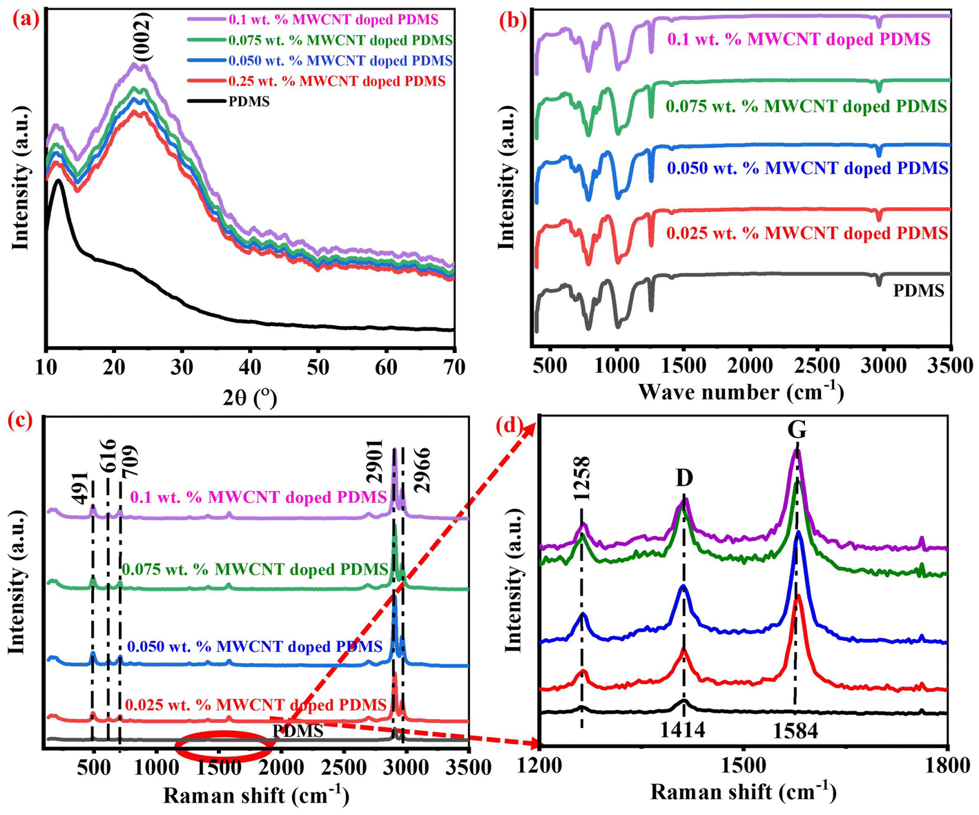 | ||
| Fig. 1 Material characterization of the spin-coated PDMS–MWCNT composite membrane. (a) X-ray diffraction patterns, (b) FTIR spectra, (c) Raman spectra, and (d) enlarged view of the Raman spectra in the range from 1200 to 1800 cm−1. | ||
The morphology of the PDMS–MWCNT composite membranes was investigated by SEM imaging, as shown in Fig. 2. The SEM micrographs showed a homogeneous dispersion of MWCNT nanofillers inside the PDMS matrix, indicating that the nanotubes were successfully incorporated into the polymer framework.
 | ||
| Fig. 2 SEM images of (a) pristine PDMS and (b) 0.05 wt% MWCNT-doped PDMS. | ||
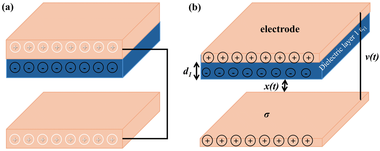 | ||
| Fig. 3 Contact-separation mode TENG: (a) structural design of the device and (b) theoretical model. | ||
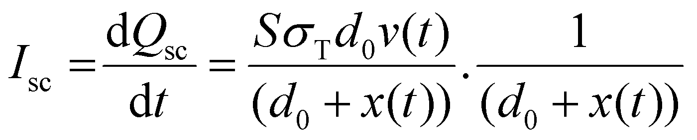
The output open-circuit voltage and short-circuit current were calculated using the parallel capacitor model, represented by the “V − Q − x” equation.29,30
 | (1) |
In open-circuit conditions Q = 0, then
 | (2) |
In short-circuit condition when the output voltage is zero
 | (3) |
 | (4) |
The electrical performances of the TENGs were evaluated by measuring the open-circuit voltage (Voc) and short-circuit current (Isc) at a frequency of 4.4 Hz, as shown in Fig. 4. The triboelectric output was measured using metal electrodes (copper and aluminium) in contact with the MWCNT-doped PDMS composite membrane. As shown in ESI Table S1 and Fig. S1,† the output performance of the copper and aluminium electrodes was comparable. Thus, copper was chosen as the electrode material for all the further triboelectric performance testing. The top electrode and friction layer had a contact surface dimensions of 20 × 20 mm2, separated by 6 mm. The output performance was investigated at different wt% of MWCNTs (0.025, 0.050, 0.075, and 0.10 wt%) in the PDMS matrix. The corresponding open-circuit voltage (Fig. 4(a–e)) and short-circuit current (Fig. 4(f–j)) values were recorded as follows: 54, 84, 110, 70, and 62 V, and 5.0, 5.8, 10.0, 6.6, and 5.8 μA, respectively. The highest Voc (∼110 V) and Isc (∼10.0 μA) were achieved at 0.050 wt% MWCNT doping, attributed to the optimized distribution of MWCNTs within the PDMS matrix at this concentration, which facilitated efficient charge transfer. The decrease in Voc and Isc were observed at wt% greater than 0.075 wt% due to exceeding the percolation threshold; whereby, beyond the percolation limit, the composite membranes started losing their properties.31 Notably, the TENG with 0.050 wt% MWCNTs exhibited nearly double the output voltage and current compared to the TENG fabricated with PDMS alone.
 | ||
| Fig. 4 Open-circuit voltage (Voc) (a–e) and short-circuit current (Isc) (f–j) of different weight percentages of MWCNT-doped PDMS. | ||
We further investigated the output performance of the 0.050 wt% MWCNT-doped PDMS at varying distances between the two triboelectric layers, ranging from 2 to 10 mm, as illustrated in Fig. 5. The highest Voc and Isc outputs were observed at a separation distance of 6 mm, as depicted in Fig. 5(a) and (d). Additionally, we studied the effect of different external pressures, ranging from 1 to 20 N. The voltage output reached a maximum of 110 V, while the current peaked at 10 μA at an applied force of 15 N, as shown in Fig. 5(b) and (e). Furthermore, we optimized the rotational velocity of the linear motor at four speeds: 20.93, 41.87, 62.8, and 83.73 rad s−1. The maximum Voc and Isc were achieved at a rotational velocity of 62.8 rad s−1, as illustrated in Fig. 5(c) and (f). Over a frequency range of 1.8 to 4.4 Hz, the open-circuit voltage (Voc) and short-circuit current (Isc) were recorded in the same way. A Voc of 55 V and Isc of 5.5 μA seen in the TENG at lower frequencies, while at higher frequencies, these went up to 110 V and 10.0 μA, respectively. The related data and graphs can be found in the ESI, in Table S2 and Fig. S2, S3.†
 | ||
| Fig. 5 V oc and Isc at different applied forces (a and d), different separation distances (b and e), and different angular velocities (c and f). | ||
To assess the energy-harvesting capability of the CS-TENG, the relationship between the output voltage (V) and load resistance (R) was measured, and the power density (P.D) was calculated using the formula P.D = V2/R·A, where A is the device area, as depicted in Fig. 6(a). The P.D was determined at a 6 mm separation between the triboelectric layers and an applied frequency of 4.4 Hz under varying external loads. The output voltage exhibited a steady increase with increasing R across the entire range. Correspondingly, the power density initially rose with the increasing R, reaching peak values of 0.2 W m−2 for pure PDMS and 0.98 W m−2 for PDMS containing 0.050 wt% MWCNTs, both at an optimal resistance of 5 MΩ. The impedance of the device was further investigated by analyzing the relationship between the voltage, current, and external load, yielding a value of 5 MΩ, as shown in Fig. 6(b). The aging effect on the TENG samples was investigated by measuring the output performance parameters weekly for 10 weeks, as illustrated in Fig. 6(c). A gradual decrease of up to 4% of output was observed after seven weeks. A maximum loss of 20% of the Voc was noticed after 10 weeks. The device output voltage was recorded across various humidity levels (ranging from 20% to 70%) and over different time intervals (up to 10 weeks) to assess the TENG's long-term stability, as shown in Fig. 6(d). Notably, the TENG generated a voltage of 110 V at 20% humidity, but the device's response significantly declined with increasing humidity. At 70% humidity, the TENG's voltage dropped to 95 V. Generally, higher relative humidity exacerbates the dissipation of triboelectric charges on the friction layers, leading to a general decrease in the output of the TENG. Further, we examined the impact of external forces and constant frequency on its output performance. Additionally, a durability test involving 10000 cycles was conducted, and the results are presented in Fig. 6(e). Remarkably, there was no degradation in the output response over the entire 10000 cycles, affirming the robustness of the fabricated TENG. This stability was particularly evident when operating at significantly lower frequencies, with minimal influence of the frequency variations. The obtained output parameters were compared with the existing available PDMS-based TENGs, as shown in Table 1.
 | ||
| Fig. 6 (a) Power density at different load resistances for all the composite membranes, (b) impendence of PDMS–MWCNT (0.050 wt%), (c) durability test of PDMS–MWCNT (0.050 wt%) over 10 weeks, (d) effect of humidity on the output voltage, and (e) durability test for 10000 cycles. | ||
| Material | Area (cm2) | Voltage (V) | Current (μA) | Impendence (MΩ) | Average power density (W m−2) | Ref. |
|---|---|---|---|---|---|---|
| PDMS/BaTiO3 | 100 | 2500 | 150 | 5 | 1.2 | 32 |
| PDMS/CNT | 6 | 77.8 | 25.7 | 3 | 3.3 | 12 |
| PDMS/SrBaTiO3 | 90 | 280 | 8.5 | 100 | 4.4 | 33 |
| PVDF/3D ZnO | 6 | 17 | 2.5 | — | — | 34 |
| Teflon-PDMS/ZIF-67 | — | 118 | 1.7 | 50 | 0.15 | 22 |
| Al/PVDF/Cu-PDMS/ITO/PET | — | 88 | 20 | 4.5 | — | 20 |
| PDMS/AGs nanowires | 20 | 33.6 | 4.5 | 8.6 | 0.23 | 21 |
| PDMS/MWCNT | 4 | 110 | 10 | 5 | 0.98 | This work |
Furthermore, the accumulated surface charge of the pure PDMS and 0.050 wt% MWCNTs was calculated using the following equation:35
Accumulated charge during one half of the AC cycle: integrates over half a cycle from t = 0 to t = T/2
 | (5) |
Substitute ω = 2πf
 | (6) |
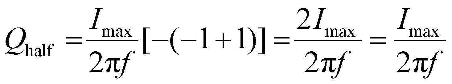 | (7) |
For PDMS

For 0.050 wt% MWCNTs

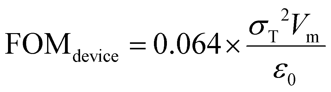
The 0.050 wt% MWCNTs showed the maximum accumulated charge and charge density of 0.25 μC and 637 μC m−2 in one complete alternating cycle. The overall performance of the proposed device was assessed by calculating the figure of merit (FOM). This parameter, influenced by the surface properties of the materials, was evaluated for both the device (FOMdevice) and the material (FOMmaterial). The calculations were carried out for pure PDMS and PDMS incorporating 0.05 wt% MWCNTs using the following expressions (8)–(13).
 | (8) |
 | (9) |
 | (10) |
| Eoutput = power × time | (11) |
| Einput = force × gap between the two plates, | (12) |
 | (13) |
2.2. Biomechanical energy-harvesting applications
Human body motion, typically characterized by low frequencies, can be effectively harvested by CS-TENGs and stored for later use. To illustrate this capability, common forms of biomechanical energy, such as hand tapping, walking, and running, were employed as examples. The circuit configuration is depicted in Fig. 7(a), where the output of the CS-TENG was connected to one terminal of a full-wave rectifier circuit, while the other terminal was left floating. The rectified output was then utilized to operate a stopwatch powered by the TENG. In Fig. 7(b), it can be seen that the rectified output was also connected to various capacitors, ranging from 1.0 to 10.0 μF, for charging purposes. These capacitors can subsequently power electronic devices. A 1 μF capacitor was charged to 4.2 V within 120 s, causing a group of LEDs to illuminate, as shown in figure and Video S1.† Furthermore, the TENG device was integrated into a shoe and tested under different human motion conditions, such as walking, jogging, and running. The device generated output voltages of 5, 10, and 20 V, respectively, for these activities, as shown in Fig. 6(c) and (d). | ||
| Fig. 7 Applications of TENG devices. (a) Schematic of a TENG used for charging a stopwatch, (b) demonstration of a capacitor charging using a TENG, (c) architectural design of a TENG integrated into a shoe for wearable applications, and (d) output voltage performance under different motion conditions, including walking, jogging, and running. | ||
The TENG device was employed to trigger an action—specifically, toggling an LED, as shown in Fig. 8(a). When subjected to an applied force, the TENG device generated voltage spikes, each comprising a positive voltage peak followed by a negative one. The amplitude of these spikes varied depending on the magnitude of the applied force. To ensure compatibility with the microcontroller's logic level, the voltage spikes were processed through a full-wave rectifier, which converted all the negative voltage peaks into positive ones to produce a unidirectional voltage signal, as illustrated in Fig. 8(b) and (d).
 | ||
| Fig. 8 Further applications of the TENG. (a) Action trigger mechanism illustrated with an LED response, (b) representation of a TENG device along with its circuit schematic, (c) visual depiction of the sensing device setup, and (d) demonstration of the response mechanism based on the applied logic. | ||
A forward-biased LED was then used to clip the maximum voltage to 2.2 V, protecting the microcontroller from excessive voltage levels. The microcontroller continuously monitored the rectified and clipped voltage via its analog-to-digital converter (ADC). When the input voltage exceeded the threshold of 2.0 V, the microcontroller toggled the state of an external LED connected through a current-limiting resistor. An LED could then be controlled by an HMI system to switch on and off.37 This configuration enabled reliable detection and response to the force-induced voltage spikes generated by the TENG device. A visual depiction of the sensing device setup is shown in Fig. 8(c) and Video S2.† This demonstration showcased the potential of the TENG as a self-powered sensor in the HMI system.
3. Conclusions
To summarise, we developed a composite PDMS–MWCNT-based TENG that demonstrated improved triboelectric characteristics. By integrating 0.025, 0.050, 0.075, and 0.10 wt% of MWCNTs into the PDMS matrix, several different composite PDMS–MWCNT membranes were created. The composition that included 0.050 wt% of MWCNTs demonstrated the most impressive performance among the five TENG samples. It was able to achieve a maximum power density of 0.97 W m−2, Isc of 10.0 μA, and Voc of 110 V. It was found that the better charge transfer that was made possible by the MWCNTs acting as a conductive filler was responsible for the increased triboelectric output. In addition, the TENG demonstrated remarkable stability, maintaining a consistent performance over 10000 cycles. The fabricated TENG was integrated with the human body to harvest output voltage signals generated during various human motions, demonstrating its potential for signal-sensing applications under applied forces.
4. Materials and methods
4.1. Synthesis of the nanocomposite films
The nanocomposite films were fabricated by combining PDMS (Sylgard 184) acquired from Jain Chemicals with MWCNTs with an outer diameter ranging from 20 to 30 nm, procured from Nano Shel, Inc., India.4.2. Synthesis of the pure PDMS film
A PDMS film was developed by combining the elastomer and curing agent in a 1:10 weight ratio. After physically combining the components for 10 min, the mixture underwent sonication for 20 min to remove any air bubbles. Subsequently, it was poured into a hollow that had been created on a sheet covered with copper. It was then evenly distributed using a spin coater. The film underwent thermal treatment on a hot plate at a temperature of 100 °C for 2 h and then underwent post-treatment at room temperature for 6 h.
4.3. Synthesis of the MWCNT–PDMS composite film
The PDMS–MWCNT membrane was fabricated by dispersing MWCNTs in a chloroform solution. In the process of creating the PDMS–MWCNT composite, MWCNTs were first dissolved in 10 mL of chloroform at a concentration of 0.5 mg mL−1. Following vacuum desiccation, the chloroform was allowed to evaporate at room temperature. Sonication was used for 20 min to volatilize the chloroform. The PDMS base was then mixed with the PDMS curing agent at a weight ratio of 10:1. To get rid of any air bubbles, the PDMS mixture was sonicated for a further 20 min. Following that, it was poured into a hollow mould made on a copper-coated sheet and left to cure for 2 h at 100 °C on a hot plate.
4.4. Fabrication of the CS-TENG
The fabrication process of the CS-TENG is illustrated in Fig. 8. Initially, a copper-clad sheet with an area of 16 cm2 was cleaned using acetone and ethanol to remove any dust particles from its surface. The cleaned sheet was then placed on a spin coater, vented, and rotated at a speed of 200 rpm for 120 s. A prepared MWCNT–PDMS composite solution was carefully dropped onto the surface of the copper-clad sheet. Once the solution was uniformly dispersed across the surface, the sheet was removed from the spin coater and dried on a hot plate at 80 °C for 2 h. After drying, the sample was cut into smaller pieces with an area of 4 cm2 as shown in Fig. 9. For CS-TENG operation, two surfaces are required to facilitate contact electrification. Therefore, two materials were selected: the composite film, which served as the negative triboelectric material, and copper, chosen as the positive material based on the triboelectric series. Copper was selected as the electrode material in the PDMS–MAX phase-based TENG, even though it is slightly less negative than aluminium in the triboelectric series. While aluminium could potentially offer higher triboelectric output due to its greater polarity difference with PDMS, copper presents several advantages that make it more suitable for practical applications.38 For instance, it offers excellent electrical conductivity, better resistance to oxidation, and enhanced chemical stability, which are critical for maintaining consistent performance over time. Additionally, copper provides stronger adhesion to both PDMS and MAX phase materials, improving the mechanical robustness and durability of the device under repeated use. Further, the oxidation potential of copper and aluminium are −0.34 and −1.66 V, respectively, indicating that aluminium has a higher tendency of getting oxidized than copper, which would not be good for the electrode over a long lifetime. These factors make copper a more reliable and efficient choice for flexible and wearable triboelectric nanogenerators. A conductive layer was established by connecting a jumper wire at the interface at the positive and negative triboelectric layers. Finally, the device was connected to a measuring instrument via two wire terminals to evaluate its output performance.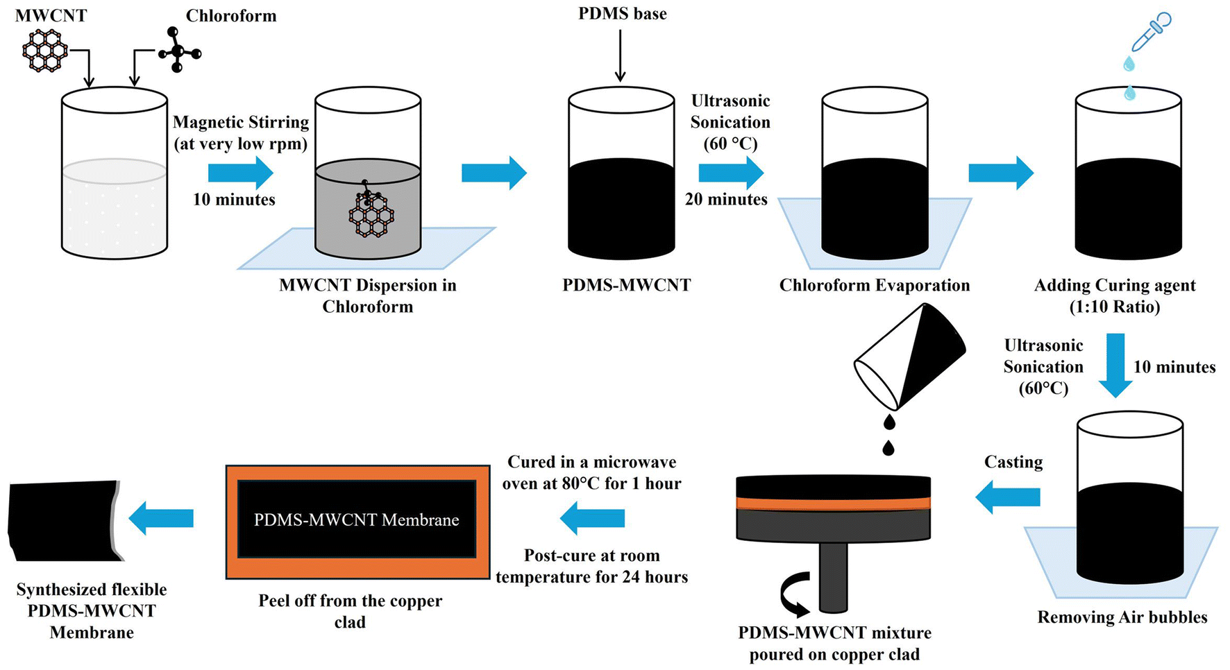 | ||
| Fig. 9 Fabrication procedure for the flexible PDMS–MWCNT composite membrane. | ||
4.5. Working mechanism of the TENG
The working mechanism of the CS-TENG is illustrated in Fig. 10. In state 1, the triboelectric layers are not in touch, resulting in no transmission of charge across the two electrodes. By the triboelectric effect, charge transfer occurs between one layer and another layer in state 2, provided that an external load is applied to the system. With the removal of the external load, the triboelectric materials begin to separate from one another, which results in a distribution of the electrical equilibrium. Additionally, as both materials begin to separate from one another, the output voltage tends to grow. By restoring the composite polymer to its original form whenever both components are completely separated from one another, we can achieve the highest possible output voltage, as seen in state 4. When we apply the external load once again, the voltage tends to decrease, as shown in state 5. Between the triboelectric layers, this method consistently displays an alternating current (AC) electrical output.24 | ||
| Fig. 10 Distribution of the transient charge in each tribological layer in a sequential manner, along with the operating principle of the device. | ||
4.6. Characterizations details
The structural properties of the synthesized materials were determined by X-ray diffraction (XRD), utilizing a Rigaku X-ray diffractometer and Cu Kα radiation (λ = 1.54 Å) in the angular range of 10°–70° at a scanning rate of 3° min−1. A Raman spectrum was produced using a Wi Tech alpha 300R confocal Raman microscope, a laser with a wavelength of 532 nm, an integration time of 10, and a 100× objective. The PDMS membrane and the PDMS–MWCNT composite membrane were examined using Fourier transform infrared spectroscopy (FTIR). The scanning was carried out with the assistance of a VERTEX 80v instrument (Bruker, Germany) that was fitted with a horizontal attenuated total reflectance (ATR) assessor. The scanning was carried out at room temperature in the wavenumber range of 3500–300 cm−1.Data availability
The data that support the findings of this study are available within the article and its ESI.†Conflicts of interest
The authors have no conflicts to disclose.Acknowledgements
The authors express their gratitude to the National Research Facility and Central Research Facility at the Indian Institute of Technology Delhi for the XRD measurement. This research was funded by SERB-DST, CRG (CRG/2023/006778), FIST (SR/FST/ET-I/2020/628), SEED Grant, FIRP, and MFIRP grant from IIT Delhi. The experiment was conducted in the Advanced Electronics Materials and Systems (AEMS) laboratory, Department of Materials Science and Engineering, IIT Delhi.References
- F. K. Shaikh and S. Zeadally, Renewable Sustainable Energy Rev., 2016, 55, 1041–1054 CrossRef.
- K. V. Selvan and M. S. M. Ali, Renewable Sustainable Energy Rev., 2016, 54, 1035–1047 CrossRef.
- X. S. Meng, G. Zhu and Z. L. Wang, ACS Appl. Mater. Interfaces, 2014, 6, 8011–8016 CrossRef CAS PubMed.
- M.-K. Kim, M.-S. Kim, S. Lee, C. Kim and Y.-J. Kim, Smart Mater. Struct., 2014, 23, 105002 CrossRef.
- F. R. Fan, W. Tang and Z. L. Wang, Adv. Mater., 2016, 28, 4283–4305 CrossRef CAS PubMed.
- K. Ylli, D. Hoffmann, A. Willmann, P. Becker, B. Folkmer and Y. Manoli, Smart Mater. Struct., 2015, 24, 025029 CrossRef.
- K. R. Kaja, S. Hajra, S. Panda, M. A. Belal, P. Pakawanit, N. Vittayakorn, C. Bowen, H. Khanbareh and H. J. Kim, Adv. Sustainable Syst., 2024, 2400678 CrossRef.
- D. Zhang, D. Wang, Z. Xu, X. Zhang, Y. Yang, J. Guo, B. Zhang and W. Zhao, Coord. Chem. Rev., 2021, 427, 213597 CrossRef CAS.
- S. Kumar, R. K. Jha, U. Chitnis, S. Singh, J. K. Anand, S. K. Roy and A. Goswami, J. Vac. Sci. Technol., B, 2023, 41, 032806 CrossRef CAS.
- A. Thakur and P. Devi, Nano Energy, 2022, 94, 106927 CrossRef CAS.
- J. Du, L. Wang, Y. Shi, F. Zhang, S. Hu, P. Liu, A. Li and J. Chen, Sensors, 2020, 20, 4523 CrossRef CAS PubMed.
- M.-K. Kim, M.-S. Kim, H.-B. Kwon, S.-E. Jo and Y.-J. Kim, RSC Adv., 2017, 7, 48368–48373 RSC.
- J. H. Kim, J.-Y. Hwang, H. R. Hwang, H. S. Kim, J. H. Lee, J.-W. Seo, U. S. Shin and S.-H. Lee, Sci. Rep., 2018, 8, 1375 CrossRef PubMed.
- X. Xia, J. Chen, G. Liu, M. S. Javed, X. Wang and C. Hu, Carbon, 2017, 111, 569–576 CrossRef CAS.
- Q.-J. Sun, Y. Lei, X.-H. Zhao, J. Han, R. Cao, J. Zhang, W. Wu, H. Heidari, W.-J. Li and Q. Sun, Nano Energy, 2021, 80, 105521 CrossRef CAS.
- D.-K. Lee, J. Yoo, H. Kim, B.-H. Kang and S.-H. Park, Materials, 2022, 15, 1356 CrossRef CAS PubMed.
- D. A. Vartak, Y. Ghotekar, P. M. Bhatt, B. Makwana, H. Shah, J. Vadher and B. Munjal, J. Environ. Nanotechnol., 2022, 11, 11–21 CrossRef CAS.
- E. W. Fenta and B. A. Mebratie, Heliyon, 2024, 10, 2405–8440 Search PubMed.
- M. Salauddin, S. S. Rana, M. Sharifuzzaman, M. T. Rahman, C. Park, H. Cho, P. Maharjan, T. Bhatta and J. Y. Park, Adv. Energy Mater., 2021, 11, 2002832 CrossRef CAS.
- X. Yang, P. Li, B. Wu, H. Li and G. Zhou, Curr. Appl. Phys., 2021, 32, 50–58 CrossRef.
- H. Zhu, J. Liang, W. Long, F. Zeng, X. Zhang and Z. Chen, J. Mater. Chem. C, 2024, 12, 1782–1791 RSC.
- S. Hajra, M. Sahu, A. M. Padhan, J. Swain, B. K. Panigrahi, H.-G. Kim, S.-W. Bang, S. Park, R. Sahu and H. J. Kim, J. Mater. Chem. C, 2021, 9, 17319–17330 RSC.
- E. Papachristou, D. Korres, D. Mamma, D. Kekos, P. A. Tarantili and G. Polyzois, J. Compos. Sci., 2022, 6, 195 CrossRef CAS.
- A. Kaur, S. Singh, P. Sharma, A. Gupta and G. Sapra, Mater. Today Commun., 2022, 33, 104742 CrossRef CAS.
- C. Rigo, E. d. C. Severo, M. A. Mazutti, G. L. Dotto, S. L. Jahn, A. Gündel, M. M. Lucchese, O. Chiavone-Filho and E. L. Foletto, Mater. Res., 2017, 20, 311–316 CrossRef.
- D. Cai, A. Neyer, R. Kuckuk and H. M. Heise, J. Mol. Struct., 2010, 976, 274–281 CrossRef CAS.
- S. Mohan, O. S. Oluwafemi, S. P. Songca, D. Rouxel, P. Miska, F. B. Lewu, N. Kalarikkal and S. Thomas, Pure Appl. Chem., 2016, 88, 71–81 CrossRef CAS.
- S. Kumar, R. K. Jha, P. Sharma and A. Goswami, Rev. Sci. Instrum., 2024, 95, 035002 CrossRef CAS PubMed.
- S. Niu, S. Wang, L. Lin, Y. Liu, Y. S. Zhou, Y. Hu and Z. L. Wang, Energy Environ. Sci., 2013, 6, 3576–3583 RSC.
- Z. Wang, J. Cui, T. Liu, S. Bai, C. Hao, Y. Zheng and C. Xue, IEEE Sens. J., 2023, 23, 1558–1748 CrossRef PubMed.
- G. Liu, Y. Chen, M. Gong, X. Liu, Z.-K. Cui, Q. Pei, J. Gu, C. Huang and Q. Zhuang, J. Mater. Chem. C, 2018, 6, 10829–10837 RSC.
- D. Tantraviwat, M. Ngamyingyoud, W. Sripumkhai, P. Pattamang, G. Rujijanagul and B. Inceesungvorn, ACS Omega, 2021, 6, 29765–29773 CrossRef CAS PubMed.
- M. V. Paranjape, S. A. Graham, P. Manchi, A. Kurakula and J. S. Yu, Small, 2023, 19, 2300535 CrossRef CAS PubMed.
- P. Pandit, M. Y. Chougale, D. Dubal, Y. K. Mishra, G. Kerr and A. K. Pandey, Small, 2025, 2408414 CrossRef CAS PubMed.
- S. Kumar, R. K. Jha, B. Thakur, T. Biswas, J. K. Anand, C. Soren, D. Banswar, S. Singh, S. Singh, S. S. Ray and A. Goswami, J. Mater. Chem. A, 2025, 13, 7786–7803 RSC.
- Y. Zi, S. Niu, J. Wang, Z. Wen, W. Tang and Z. L. Wang, Nat. Commun., 2015, 6, 8376 CrossRef CAS PubMed.
- B. Zhang, Y. Tang, R. Dai, H. Wang, X. Sun, C. Qin, Z. Pan, E. Liang and Y. Mao, Nano Energy, 2019, 64, 103953 CrossRef CAS.
- Z. L. Wang, ACS Nano, 2013, 7, 9533–9557 CrossRef CAS PubMed.
Footnote |
| † Electronic supplementary information (ESI) available. See DOI: https://doi.org/10.1039/d5lp00076a |
| This journal is © The Royal Society of Chemistry 2025 |