DOI:
10.1039/D4MA00960F
(Paper)
Mater. Adv., 2025,
6, 168-183
Improvement of hydrophilicity and optical nonlinearity in a Te/In2Se3 bilayer heterostructure film by annealing at different temperatures for optoelectronic applications†
Received
23rd September 2024
, Accepted 15th November 2024
First published on 15th November 2024
Abstract
Group III–VI semiconductor materials have unique properties for photodetector and optoelectronic devices. The present work is based on the formation of Se–In–Te alloys from the bilayer Te/In2Se3 heterostructure by annealing at various temperatures. The heterostructure and its conversion to a layer alloy were verified from the cross-sectional view taken by FESEM. The surface morphology shows a reduction in nanoparticle size with annealing temperature. EDX confirmed the In, Se, and Te existence in the film structure. The existence of different phases of In2Se3 and Te was found from the structural investigation through XRD and HRTEM. The increase in crystallinity and decrement in dislocation density influenced the optical properties of the film by reducing the transmittance by 50% and increasing the extinction coefficient upon annealing. The optical density increased with a decrease in optical bandgap upon annealing, thus increasing the refractive index. The hydrophilicity nature increased to a super hydrophilic one at a high annealing temperature. The χ(3) value increased from 1.164 × 10⁻¹⁰ to 1.680 × 10⁻¹⁰ esu, and the nonlinear refractive index enhanced from 1.244 × 10⁻⁹ to 1.721 × 10⁻⁹ esu upon annealing. The change in photoconductivity upon annealing is very useful for visible light photodetection.
1. Introduction
Group III–VI-based semiconducting In–Se chalcogen-based compounds are the leading applicants for various solid-state devices like phototransistors, optoelectronic, photodetectors, and thermoelectric ones.1–4 The addition of another chalcogen element like Te into the In–Se matrix makes it more applicable in various ways such as photovoltaics, electrical switching, and phase change memory applications.5,6 The inclusion of such a dopant turns acts as a chemical modifier by bringing the disorder (compositional) that leads to the change in the electrical properties of chalcogenides.7 Metal doping in chalcogenides bring numerous changes in their properties and is useful for various optoelectronic applications.8 The substitution of Te into In–Se lowers its bandgap, which is appropriate for solar cell absorbing material. The thermal as well as electrical switching behavior of Se86−xTe14Inx compounds is suitable for electronic devices. Among these, Se80Te14In6 comes out to be the fastest phase-change material. It has an Ith value of 1.3 mA as the memory-switching current threshold and 49.2 V as the threshold voltage.6 The indium-added Se–Te films of the Se75−xTe25Inx system are good for optical disk making.9 The existence of ion-covalent bonds in Se80Te20–xInx films increases the thermal conductivity and thermal diffusivity.10 In2(Te1−xSex)3 is a layered compound from the AIII2BII3 family with a disordered structure and cation vacancies. The ion irradiation on such films forms defects inside the films and leads to enhanced electrical transport properties for better thermoelectric performance.11 The annealed In10Se70Te20 thin films showed an increase in crystallinity with In2Te3 and In2Se3 phases that increased the energy gap and reduced the refractive index upon annealing. The tuning in the optical characteristics of In10Se70Te20 films is used for non-linear optics.12 The electrons and holes are localized in the InSe and InTe layers for the InSe/InTe van der Waals heterostructure. It shows intrinsic type-II band alignment. The conversion from type-II to type-I band alignment makes it suitable for light-emitting devices. The flexibility of such two-dimensional InSe/InTe vdW heterostructure paves the path for future optoelectronic devices.13 The electronic excitation in In2(Te0.94Se0.06)3 n-type films improves the material for better thermoelectric performance.14 The systematic increase in current with temperature in In2(Te1−xSex)3 films indicates its semiconducting nature. Such films have low activation energy, which is suitable for phase change memory applications.15
There are various ways to prepare the In–Se–Te composite films, like conventional melt quenching and thermal evaporation methods. However, the diffusion of dopant into the host matrix also forms ternary compounds through external energy sources like ion irradiation, laser annealing, and thermal annealing.16–18 Light-induced Te diffusion onto As2S3 film reduces the optical bandgap by forming different homopolar bonds. Such changes are because of the change in the density of states and disorder in the system.19 The solid solution of As–Se–Te forms from the Te/As50Se50 bilayer structure upon irradiation with near-band-gap laser light. This solid solution has a reduced band gap in the diffused region with an increase of density of states at the band edge.20 Among these methods, thermal annealing is considered the low-cost, easy, and safe way for the dopant introduction into the host materials. The annealed films have larger nonlinear parameters like refractive index and 3rd-order nonlinear susceptibility, which makes them suitable for phase-change material-based optoelectronic applications.21 The formation of a mixed phase of In/Se and In2Se3 after 300 °C annealing makes the film a polycrystalline one with a reduced bandgap of 2.82 eV.22 The Bi inclusion into the In2Se3 layer forms Bi2Se3, Bi4Se3, and BiSe phases at the interface. The σopt, σelect, and refractive index changed significantly and were found suitable for making multifunctional optoelectronic devices.23 The Ag/In/Ag/In multilayer stack upon annealing forms the AgInSe2 and impurity Ag2Se phases. The resulting alloy behaves like an n-type conduction mechanism with reduced resistance and increase in temperature. The newly formed AgInSe2 from Ag/In/Ag/In multilayer is suitable as an absorbing material for solar cell devices.24 Therefore, thermal annealing plays a pivotal role in bringing the desired changes in the sample as per requirement.
The annealing temperature influences the Te diffusion into Ni, which affects the reaction product. The penetration depth of Te increases as the annealing temperature is enhanced from 500 °C to 1000 °C. The obtained surface reaction product comes out as NiTe0.67 (Ni3Te2) or a mixture of NiTe0.69.25 The formation of CdTe1−xSx ternary compound at the CdTe–CdS interface is due to the Te interdiffusion into the CdS layer through post-thermal annealing.26 Similarly, the formation of CdS1−yTey through Te diffusion into the CdS layer resulted in a band gap less than that of CdS. This caused an increase in light absorption in the window layer with a reduction in the Jsc of the device.27 The carrier concentration changed with a reduction in thermal conductivity by keeping the structure and composition the same in Te evaporated annealed samples. Looking at the importance of Te inclusion into various host matrices, the current investigation lies in the diffusion of Te into In2Se3 films at various annealing temperatures (100 °C, 150 °C, 200 °C, and 250 °C). The structural, optical, and morphology changes are dependent on the annealing temperatures. The optimized parameters were determined through various experimental techniques on these films.
2. Film preparation and experimental characterizations
2.1. Te/In2Se3 film preparation
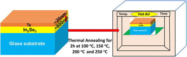
The bilayer Te/In2Se3 film structure was prepared from high purity (99.999%) Te and In2Se3 powders purchased from Sigma Aldrich. The bottom In2Se3 layer of ∼800 nm was grown on the glass substrate (cleaned one) by the thermal evaporation method at a 0.5 Å s−1 deposition rate. The deposition chamber was under a vacuum of 10−5 torr. The thickness of the layers was monitored through a thickness controller. The substrate holder was on continuous rotation by a slow-speed motor for uniform and smooth film deposition. The same procedure was repeated for the deposition of the Te layer of ∼20 nm on the prepared In2Se3 film layer. The schematic diagram of the film structure and annealing of the films are shown in Scheme 1.
 |
| | Scheme 1 Schematics of Te/In2Se3 film and annealing procedure. | |
2.2. Experimental characterizations
Cross-sectional field emission scanning electron microscopy (FESEM) (JEOL-SEM-7601F) was used to verify the formation of the bilayer structure. The cross-sectional view was captured at an operating voltage of 30 kV at a high vacuum. FESEM was used to image the surface morphology of the films after different annealing treatments. Te, In, and Se in both annealed and as-grown films were verified from energy dispersive X-ray (EDX) analysis. The EDX unit also used elemental mapping, which presents the uniform spreading of different elements. The morphology and structural changes were further confirmed through high-resolution transmission electron microscopy (HRTEM, JEM-2100-HRTEM) pictures.
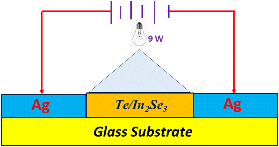
The planes corresponding to the different phases present in the sample were mapped using selected area electron diffraction pattern (SAED). TEM was conducted on the 250 °C annealed film. Structural modifications were investigated using a Brucker-D8 advance X-ray diffraction (XRD) unit. The Cu-Kα source (λ = 1.541 Å) was employed as the X-ray source. Data was collected at a step size of 0.02° s−1 with a glancing angle of 1° from 10° to 70°. Raman spectroscopy was done using a HORIBA Raman spectrometer (1024 × 256 OE) with a 632 Helium–Neon nm laser source and a CCD detector for taking data from 50–500 cm−1. A UV-visible spectrophotometer from JASCO V-770 was employed to record the transmission data between 1200–2500 nm with a resolution of 0.5 nm. Various theoretical formulas were used to evaluate linear–nonlinear optical factors from the transmittance data. A DMe-211 Plus contact angle meter was employed to take the data at a temperature of 25–27 °C with 25–35% relative humidity. The 1 μL liquid droplet was formed at the end of the syringe, which was brought in contact with the film surface. The static image was recorded just after the withdrawal of the syringe within 3 s by a charge-coupled device (CCD) camera. The presented data is based on 4–6 repetitions. The Keithley 2450 Source Measure Unit was used to measure the current over −10 to 10 V at a 0.03 V step size. The readings were taken multiple times to reproduce the measurement. A 9-W white LED bulb was used to take the photo response under light–dark conditions (Scheme 2).
 |
| | Scheme 2 Schematic for I–V measurement of the films. | |
3. Result analysis
3.1. Surface morphology by FESEM, EDX, and TEM study
The Te/In2Se3 bilayer film structure is viewed from the cross-sectional FESEM (Fig. 1) images. The as-grown and annealed film thicknesses are well observed from the layer structure. The as-prepared Te/In2Se3 film has a thickness of ∼789 nm for the bottom In2Se3 layer, while the top layer Te has a thickness of ∼29 nm, as shown in Fig. 1a. The Te top layer was not uniform due to the small thickness value deposited within a short time duration. The thickness of the 250 °C annealed film is shown in Fig. 1b, which offers a single layer resulting from intermixing the two layers with heat energy. The film thickness remains nearly the same (slight reduction of ∼3 nm) after annealing, which infers that there is no change in the thickness of the film with heat treatment in this case. Heat treatment may improve the film microstructure due to intense crystalline growth without affecting the film thickness.
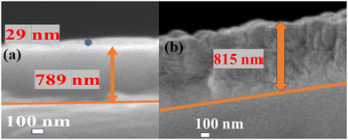 |
| | Fig. 1 Cross-sectional FESEM image of Te/In2Se3 (a) as-prepared (b) 250 °C annealed film. | |
The elemental mapping technique gives valuable data on the composition and uniformity of the film. Fig. 2 illustrates the In, Se, and Te mapping of the as-deposited film. The presence of every element has been confirmed, and the elemental mapping of the thin film sample demonstrates the homogenous distribution of all three elements inside the film. The elemental mapping for the 250 °C film is presented in Fig. S1 (ESI†).
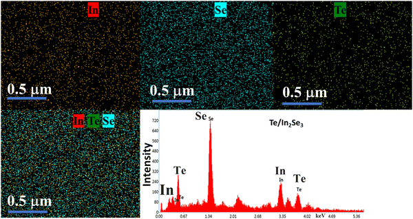 |
| | Fig. 2 EDX mapping and spectra of as-prepared Te/In2Se3 film. | |
Fig. 2 shows the EDX spectra for the as-deposited Te/In2Se3 film, which have prominent peaks that refer to the existence of different elements. The intensity versus energy plot represents the shell energies of the material components. The small peaks near 0.277 keV are for carbon (C). This was taken during imaging for charge correction. The peaks near 1.34 keV belong to the Se-atoms. The In and Te peaks are located near 3.35 keV and 3.91 keV, respectively. Another small In peak is located near 0.5 keV. Extra low-intensity Au peaks are found at 2.132 keV, which was used for coating the samples during imaging process. Fig. S2 (ESI†) presents EDX spectra for Te/In2Se3 films annealed at 100, 150, 200, and 250 °C. The elemental composition, both atomic and weight%, is presented in Table S1 (ESI†).
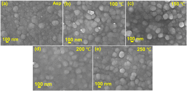
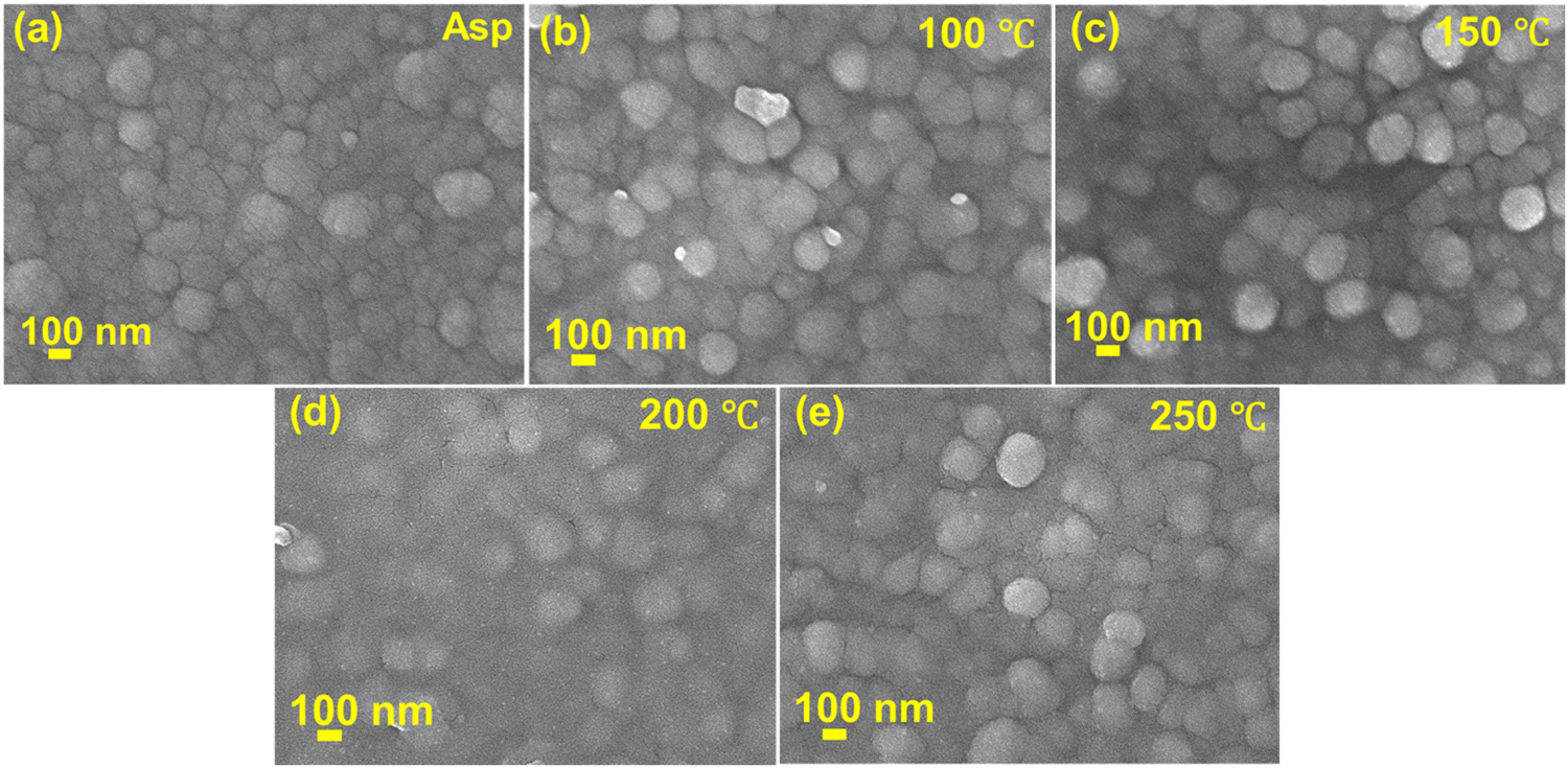
FESEM is a salient tool that plays a crucial role in the characterization of films, offering valuable insights into their structure, morphology, and properties. Fig. 3(a–e) depicts the FESEM images of both the as-prepared and annealed thin films at a 100 nm magnification. The images demonstrate the consistency of the films. The morphology of the films were found to be nanoparticles, which remained unaltered even after increasing the annealing temperature from 100 °C to 250 °C. The FESEM images of all the samples (both as-prepared and annealed) at a 1 μm magnification are presented in Fig. S3(a–e) of the ESI.†
 |
| | Fig. 3 FESEM images of Te/In2Se3 films at different conditions at 100 nm. | |
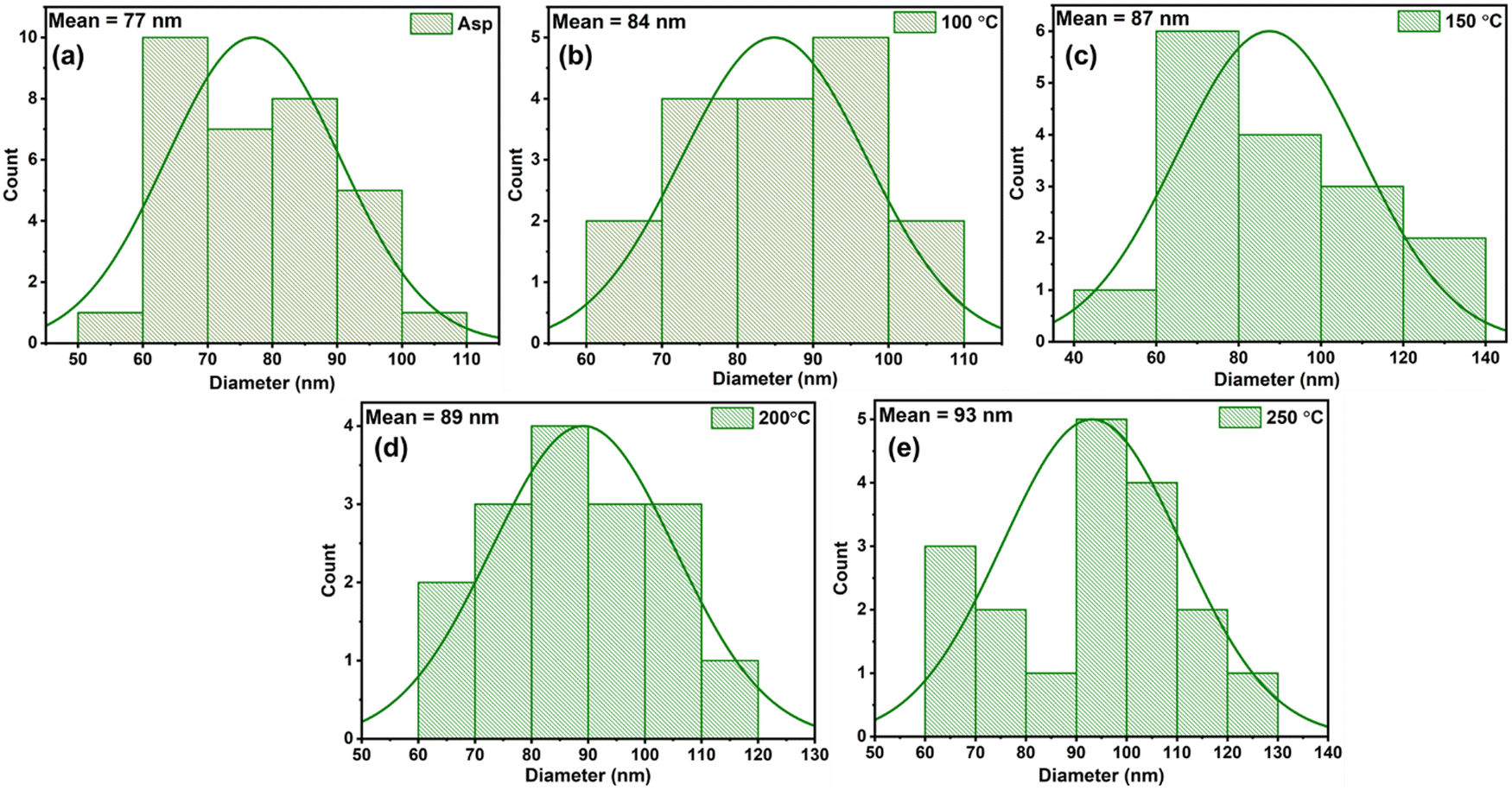
The average particle sizes for all the films have been calculated and illustrated in Fig. 4. It comes out to be 77, 84, 87, 89, and 93 nm for the as-prepared and 100, 150, 200, and 250 °C annealed thin films, respectively. The nanostructured particle size was found to increase with annealing temperature, demonstrating surface modification during annealing. This increase in particle size due to annealing might be attributed to thermal expansion, whereby the increase in annealing temperatures leads to an augmentation in the kinetic energy of atoms. The variation in particle size of the as-prepared as well as annealing temperatures is given in Fig. S5 (ESI†).
 |
| | Fig. 4 Particle size distribution of Te/In2Se3 films at different conditions. | |
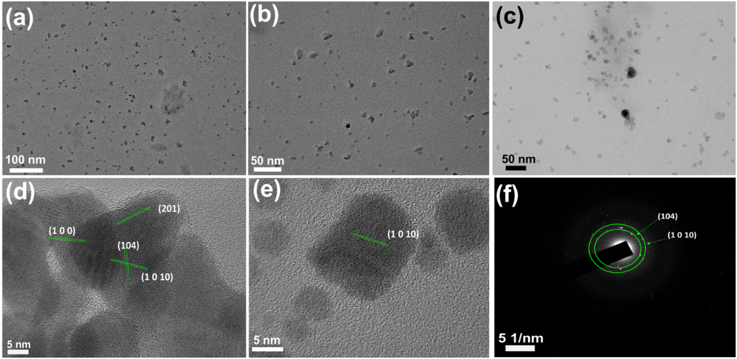
TEM study of the material gives good insight into the morphology and structural properties. Fig. 5 represents the TEM images of the 250 °C annealed Te/In2Se3 thin films. Fig. 5(a–c) presents the TEM images for the thin films at various scale ranges. Fig. 5(d) illustrates the HRTEM image, which confirms the presence of various phases such as (1 0 0) and (2 0 1) of the Te phase with the d-spacing values in the range of 3.79 Å and 1.95 Å, respectively. Similarly, other planes such as (1 0 4) and (1 0 10) confirm the In2Se3 phases with d-spacing of 3.19 Å and 2.24 Å, respectively. Fig. 5(e) confirms the presence of the (1 0 10) plane of In2Se3 with a ‘d’ value of 2.24 Å. The SAED pattern of the annealed thin film is illustrated in Fig. 5(f), which confirms the existence of two In2Se3 planes, (1 0 4) and (1 0 10), agreeing with the XRD results. The TEM image, HRTEM image, and SAED pattern of the as-prepared thin film has also been illustrated in Fig. S4 (ESI†). Fig. S4(a) and (b) (ESI†) illustrates the TEM images of the as-prepared Te/In2Se3 thin film sample at 50 and 100 nm respectively. Moreover, the HRTEM image of the sample has been depicted in the Fig. S4(c) (ESI†). Furthermore, the SAED pattern of the sample has been shown in Fig. S4(d) (ESI†). It can be clearly understood that no significant changes occurred to the morphology of the films. In both as-prepared and annealed cases, the morphology can be observed to be nanoparticles, confirming the FESEM results. The intense (1 0 4) plane further supports the In2Se3 phase, which can be observed from Fig. S4(c) (ESI†).
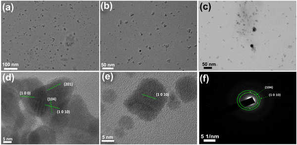 |
| | Fig. 5 (a)–(c) TEM images, (d) and (e) HRTEM images, and (f) SAED pattern of the 250 °C annealed Te/In2Se3 thin films. | |
3.2. XRD and Raman analysis
The XRD pattern of Te/In2Se3 films at different conditions is illustrated in Fig. 6(a). In the current report, Te is deposited over the In2Se3 in the 20 nm range. The as-grown and annealed films show both In2Se3 and Te phases. For the as-grown film, the peaks appeared near 28.16°, 40.46° and 42.76° correspond to the In2Se3 rhombohedral phase (ICSD: 01-072-1470), which corresponds to the (1 0 4), (1 0 10) and (0 1 11) planes. Other peaks appeared around 22.87°, 49.67°, 63.45° and 65.82° corresponding to hexagonal Te phase (00-001-1313), representing the (100), (201), (210), and (211) planes, respectively. A similar pattern is observed for 100 °C, 150 °C, and 200 °C annealed films, with an increment in the peak intensities. However, for the 250 °C annealed thin films, various smaller intensity peaks appeared around 28.96°, which corresponds to the In2Se3 phases of the material. This enhancement in the peak intensities and formation of new peaks after annealing confirms the increment in the crystallinity of the material. Since annealing provides the energy required for atomic rearrangement, it might improve the crystalline structure of tellurium. Te atoms consequently become more structured, which increases crystallinity and produces intense diffraction peaks.28 There are several methods used for the calculation of different structural parameters of the thin films. In the current study, Scherrer's formula and Williamson–Hall's method have been adopted to analyze the structural behavior of the material. From Scherer's observation, the structural parameters were calculated from the relations,29| |  | (1a) |
| |  | (1b) |
| |  | (1c) |
| |  | (1d) |
where ‘λ’ is the CuKα line wavelength (1.54 Å), and θ is Bragg's angle. β represents the full width at half maximum (FWHM). The estimated parameters are listed in Table 1. XRD analysis uses the Williamson–Hall (W–H) method to retrieve data regarding the strain and size of crystalline materials. This is especially helpful when describing materials that are polycrystalline or nanocrystalline. The X-ray diffraction peak broadening is related to both crystallite size and microstrain, as per the Williamson–Hall formula.
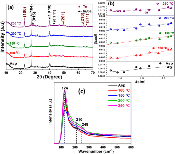 |
| | Fig. 6 (a) XRD pattern and (b) Williamson–Hall plot (c) Raman spectra of as-prepared and annealed Te/In2Se3 thin films. | |
Table 1 Estimated structural parameters of as-prepared and annealed Te/In2Se3 thin films
| Structural parameters |
Scherrer's method |
Williamson–Hall plot |
|
D (nm) |
ε (× 10 −3) |
δ (nm−2) × 10−3 |
N
c (nm−2) |
D (nm) |
ε (× 10 −3) |
δ (nm−2) × 10−3 |
N
c (nm−2) |
| Asp |
19.11 |
5.94 |
2.73 |
0.11 |
18.14 |
5.23 |
3.03 |
0.13 |
| 100 °C |
19.84 |
5.21 |
2.54 |
0.10 |
19.26 |
5.01 |
2.69 |
0.11 |
| 150 °C |
26.20 |
4.90 |
1.45 |
0.04 |
24.51 |
4.69 |
1.65 |
0.05 |
| 200 °C |
44.80 |
7.84 |
0.49 |
0.09 |
42.16 |
6.08 |
0.56 |
0.01 |
| 250 °C |
48.54 |
8.56 |
0.42 |
0.07 |
46.89 |
9.26 |
0.45 |
0.08 |
The total broadening is written as30
| | | βtotal = βsize + βstrain | (2a) |
with
βsize as the crystallite size broadening and
βstrain as broadening for strain. The Scherrer equation,

. The macro strain-induced XRD peak broadening is given by
βstrain = 4
ε![[thin space (1/6-em)]](https://www.rsc.org/images/entities/char_2009.gif)
tan
θ.
now,
| |  | (2b) |
or,
| |  | (2c) |
The W–H plot for the Te/In2Se3 films is shown in Fig. 1(b). It is evident from eqn (2c) that the crystallite size is determined by calculating the inverse of the intercept by kλ, while the slope (ε) represents the lattice strain. The structural parameters were determined using both methods, which are provided in Table 1. An elevation in annealing temperature typically leads to a notable augmentation in the crystallite size of the material. This phenomenon often involves the amalgamation of smaller particles into larger ones. As the temperature rises during annealing, the crystallite size increases. This is because fewer defects exist, which encourages grain growth and improves crystallinity.31 The underlying cause of internal stress in thin films predominantly stems from lattice defects, such as dislocations, as well as lattice mismatches with the substrate. Annealing process releases internal stresses in the thin film, which lowers defect concentrations and lattice distortions. The unit cell dimensions may change as a result of compositional changes caused by annealing, such as the addition or removal of Te atoms or Se vacancies. Furthermore, the lattice spacing is impacted by the material's thermal expansion. The crystallite size, micro strain, and lattice parameters of the annealed thin films can be strongly influenced by the lattice mismatch between the Te and In2Se3 layers as well as interactions with the sample holder during the annealing process. The strain induced at the two materials' contact as well as potential outside stresses during annealing are the causes of these effects.32 As the annealing temperature rises, there is a gradual decrement in dislocation density within the sample, leading to a discernible enhancement in the average strain. Additionally, an intriguing observation surfaced: each parameter derived from the Williamson–Hall plot exhibited values lower than those calculated using Scherrer's formula.33
Raman spectroscopy is a powerful technique for analyzing materials by looking at their molecular vibrations. The peaks are assigned to specific vibrational modes based on their wavenumbers and symmetry properties.34 The Raman spectra of the material are shown in Fig. 6c in the range of 50–600 cm−1. Different vibrational modes have been identified at 124, 210, and 248 cm−1. The 124 cm−1 peak can be attributed to the A1g mode, which is only due to the vibrational motion of Te atoms.35 The satellite peak at 210 cm−1 refers to an E-type vibration of InSe. The E-type vibration of InSe provides a specific vibrational mode where the atoms within the crystal lattice vibrate symmetrically along the axis parallel to the lattice plane.36 Furthermore, the Raman peak at 248 cm−1 refers to the optical phonon mode due to the vibration of the In and Se ions along the direction of light propagation within the thin film.37
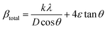
3.3. XPS study
A prominent surface analysis method for examining the fundamental composition and chemical bonding of materials is XPS. In XPS, the environment encompassing an element, such as its chemical bonding and oxidation state, is reflected in the element's core-level binding energy. The purpose of the measurement was to obtain data about the different kinds of bonds that are present in the film. The XPS spectra of the as-prepared and 250 °C annealed Te/In2Se3 thin film have been demonstrated in Fig. 7. The high-resolution XPS spectra of In 3d, Se 3d, Te 3d, and the survey spectra have been shown in Fig. 7(a–d) respectively. The binding energy values of as-prepared In 3d at 444.55 eV and 452.09 eV correlates to the In 3d5/2 and In 3d3/2, respectively, which is shown in Fig. 7(a). This corresponds to the peak-to-peak parting of 7.54 eV. It can be observed that the binding energy has shifted slightly towards higher energy in the 250 °C annealed thin film.38 Similarly, the Se 3d core level peak for the as-prepared thin film has been found to have a binding energy of 54.75 eV, which correlates to the Se 3d5/2, as shown in Fig. 7(b). The intensity increased for the annealed thin film compared to the as prepared, which signifies the Se–Se homopolar bond density.39 Meanwhile, the Te 3d core level peaks are found at binding energies of 575.28 eV and 585.63 eV, corresponding to Te 3d5/2 and Te 3d3/2, respectively. This has been illustrated in Fig. 7(c). The peak at 575.28 eV corresponds to the existence of Te2−, while the peak at 585.63 eV confirms the orbital bonding of Te, which enhances the other elements.40 Additionally, the survey spectra have been shown in Fig. 7(d) in the 0–1200 eV range. The Te 3d, In 3d, and Se 3d peaks that originate from the Te/In2Se3 thin films are apparent in the XPS survey spectra. The corresponding oxidation state and shift in the material after annealing also revealed the formation of the Te/In2Se3 thin film. Since XPS provides comprehensive information about the elemental composition and chemical state, it will help in understanding of thin film formation. Therefore, these XPS results infer the formation of the thin film and the elemental bonding.
 |
| | Fig. 7 XPS spectra of (a) In 3d, (b) Se 3d, and (c) Te 3d (d) survey spectra of as-prepared and 250 °C annealed Te/In2Se3 thin film. | |
3.4. Linear optical parameters from UV-visible study
3.4.1 Transmittance, absorption, and extinction coefficient.
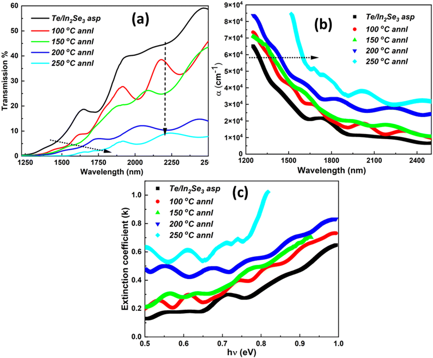
The optoelectronic parameters of the films depend on the primary data of transmittance and absorbance of the sample. The type of interaction of the incident electromagnetic wave and semiconducting film dictates the shape of the optical spectra. The transmission window for the studied film is found to be between 1500 nm and 2500 nm, as shown in Fig. 8a. The bilayer Te/In2Se3 film is found to have 60% transmission at 2500 nm wavelength, which gradually decreases upon annealing. The interdiffusion of Te into the bottom In2Se3 layer decreased the transmission by creating more scattering centers, and thermal annealing induced increased crystallites, as seen from the XRD. The transmission significantly reduced to ∼8% for the 250 °C annealed film. Such reduction in transmission indirectly increased the absorption power of the film, as seen in Fig. 8b. The absorption edge's move to a higher wavelength region upon annealing is noticeable, which indicates a decrement in the optical bandgap.
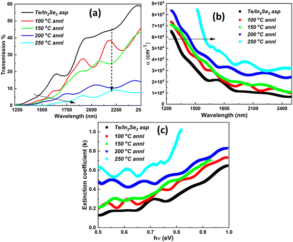 |
| | Fig. 8 (a) Transmission (b) absorption coefficient (c) extinction coefficient of the Te/In2Se3 film. | |
The absorption coefficient (α) value is evaluated from the primary transmission data (T) and by considering the thickness of the film (d) as determined from the cross-sectional FESEM in the equation41
| |  | (3) |
The ‘α’ value is within the range of 10−4 cm−1 along the entire range of the wavelength. The annealed films have higher ‘α’ values than the as-prepared Te/In2Se3 film.
The bond rearrangements occur with the breaking of weaker bonds and converting them into saturated ones upon thermal annealing. Such a process is responsible for the atomic and molecular reconfiguration inside the film.42 The increased scattering centers due to annealing caused a light loss in the film and are evaluated by the optical quantity extinction coefficient (k). The traveling electromagnetic wave inside the film attenuates with length, and its intensity changes with the absorption of light. This is expressed as an absorption index. The calculated  value varies with annealing temperature in an increased pattern, as shown in Fig. 8(c). The presence of high amounts of unsaturated bonds and defects in the chalcogenide material, are accountable for localized states. The heating of the films annealed out those unsaturated defects and created more saturated bonds. The localized state density is reduced by the decreased concentration of unsaturated defects, which affects the refractive index (n) and k values. The increase in ‘k’ with annealing is because of the change in density as ‘k’ is related to surface defects and disorder, which arise from Te diffusion into the In2Se3 layer.43
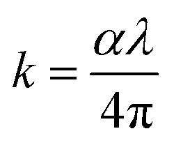
3.4.2 Optical density (OD), skin depth (δ), and bandgap (Eg).
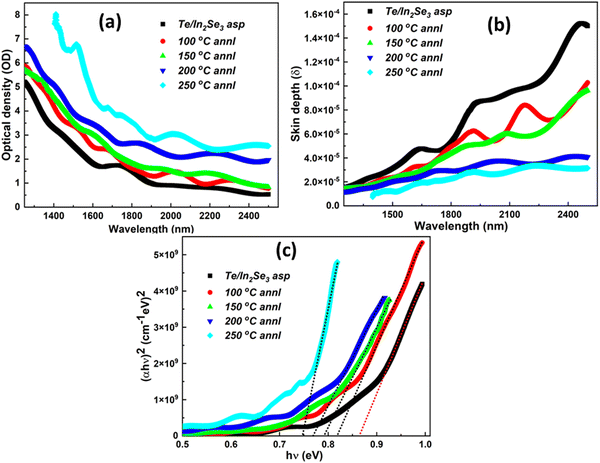
Optical density measures the absorbed light by the film and is evaluated by α × d with ‘d’ as film thickness. The variation of OD with wavelength is represented in Fig. 9a. The OD value decreased gradually with increase in wavelength, which suggests a normal dispersion behavior. Upon an increase in temperature, the OD value is enhanced with the annealing temperature. The increased value of OD at the IR region with annealing leads to increased material concentration, leading to lower transparency, as found in Fig. 8a. Such an increase also shows the carrier mobility increment, thus reducing the Eg value.44
 |
| | Fig. 9 (a) Optical density (b) skin depth (c) bandgap of the Te/In2Se3 film. | |
Skin depth measures the penetration length of the incident wave through the film. The point where the amplitude turns into 1/e times its original value is measured as the ‘δ’. It is evaluated as the reciprocal of the absorption coefficient as δ = 1/α. The decrease in δ value with annealing is presented in Fig. 9(b). The δ value also depends on the film conductivity, which is also discussed in the next section. In the present case, the bandgap is reduced with annealing, which supports the decrease in skin depth with annealing. The observed decrease in the ‘δ’ value at specific wavelength regimes allows it to make different multimode optical fibers.45
The band gap of semiconducting materials depends on absorption strength and is dominated at a higher absorption region with ‘α’ more than 104 cm−1. The dependence of the ‘α’ with photon energy follows the Tauc rule as,46
The band tailing parameter ‘B’ is called the Tauc parameter, which measures the structural randomness in a semiconductor. The exponent ‘z’ decides the transition modes in the semiconductors. If z = 2 or z = ½, and fits well to the experimental data, then it is indirect and direct allowed transition, respectively. In the current study, z = ½ fits well with the data, thus showing the directly allowed semiconductor. Fig. 9(c) demonstrates the annealing-induced bandgap variation at different temperatures from the host material. The calculated values from the linear fitting are presented in Table 2. The bandgap changed from 0.865 to 0.747 eV at 250 °C annealing. The particle size/density of defect states increase might be accountable for the reduction in band gap by annealing.47 The average particle size (D) increased with annealing, as found from XRD analysis. A decrease in Eg with annealing is interpreted as inducing crystallization in semiconducting films. The Tauc parameter reduced on annealing, thus inferring the change in the defect state density.
Table 2 Calculated optical parameters of Te/In2Se3 thin films
| Optical parameters |
Te/In2Se3 |
100 °C |
150 °C |
200 °C |
250 °C |
|
E
g (direct) eV |
0.865 |
0.821 |
0.792 |
0.768 |
0.747 |
|
B
2 (× 1010) cm−2 eV −2 |
3.37 |
3.24 |
2.72 |
2.69 |
2.51 |
|
n
0
|
3.524 |
3.578 |
3.616 |
3.648 |
3.677 |
|
ε
∞
|
12.425 |
12.806 |
13.075 |
13.309 |
13.523 |
|
η
opt
|
1.640 |
1.634 |
1.630 |
1.626 |
1.623 |
|
χ
(1)
|
0.909 |
0.941 |
0.961 |
0.980 |
0.997 |
|
χ
(3) (× 10−10 esu) |
1.164 |
1.327 |
1.452 |
1.568 |
1.680 |
|
n
2 (× 10−9 esu) |
1.244 |
1.397 |
1.513 |
1.619 |
1.721 |
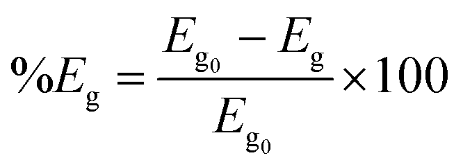
The % of Eg change (%Eg) is taken as an optical entity to study the significant change in Te/In2Se3 films after thermal annealing.48
| |  | (5) |
where
Eg0 and
Eg are the band gaps for as-deposited and annealed films. The % of
Eg change of the annealed film varies from 5.08%, 8.43%, 11.21%, and 13.64% for 100, 150, 200, and 250 °C, respectively. This change in the %
Eg of the material confirms that there is a significant change in the optical properties of the film. Hence, annealing brought alteration in the optical parameters, which enabled it for various applications.
3.4.3 Static refractive index, high-frequency dielectric constant, optical electronegativity.
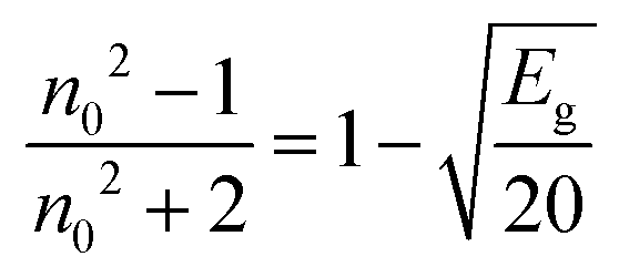
The estimated Eg value of the films is used to evaluate the static refractive index (n0) for Te/In2Se3 thin films by Dimitrov and Sakka relation49| | 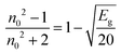 | (5a) |
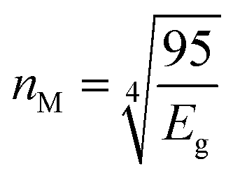
The evaluated value is found to be improved on annealing as presented in Table 2. The improvement in n0 value with a decrease in Eg is satisfied by Moss’s relation, i.e., Egn4 ≅ constant.50 The ‘n0’ values show the increasing nature of annealing. The modified Moss relation led to the relation.
| |  | (5b) |
with a ‘
k’ value of 95 eV. The relation which is applicable for materials below the bandgap values of 4 eV is developed by Ravindra as
51| | | nR = 4.084 − [0.62 × Eg] | (5c) |
This formula has limitations for very high and very low bandgap materials.
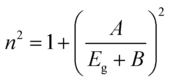
The oscillator theory-based model for low bandgap material was formulated by Herve–Vandamme52
| |  | (5d) |
here, the value of
A is 13.6 eV and
B is 3.74 eV. Tripathy established an empirical relation
53 for a wide range of frequencies which is given as
| | | nT = 1.73 × [1 + 1.9017 × e−(0.539×Eg)] | (5e) |
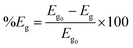
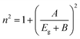
The values of the refractive index obtained from various models are shown in Fig. 10a, which shows the inverse variation with bandgap values.
 |
| | Fig. 10 (a) Theoretical refractive index variation with bandgap (b) variation of χ(3) and bandgap for different samples. | |
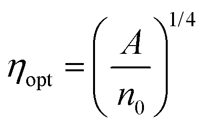
The estimated high-frequency dielectric constant (ε∞ = n02), enhanced by annealing, which measures the electrical polarizability of the compound is shown in Table 2. The optical electronegativity by Duffy relation,54 , with A = 25.54 gives information about the attractiveness of a radical or atom to electrons to form an ionic bond. The evaluated values gradually decrease from 1.640 (as-prepared) to 1.623 upon annealing at 250 °C (Table 2). The small change of 1.03% shows the stability of the annealed films on optical electronegativity.
3.5. Nonlinear optical parameters
The high nonlinear optical susceptibility possessed by the chalcogenide-based compounds makes them important for nonlinear optics. Metal chalcogenides have interesting applications as sources for coherent light, materials with higher conversion efficiency, infrared nonlinear optical materials, ultrafast switching, electro-optic modulators, and more.55 The optical polarization (P), which depends on the electric field intensity (E), establishes a relation as
It contains both linear and nonlinear terms and is expressed in the power series form like
| | | P = ε0[χ(1)E + χ(2)E2 + χ(3)E3 + …] | (6b) |
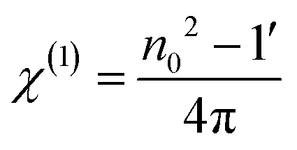
The first term is the linear polarization that contains ‘χ(1)’. The other terms contribute to nonlinear response towards the materials.56 The absence of inversion symmetry leads to the zero value of χ(2) (2nd order nonlinear susceptibility) for centrosymmetric compounds. So, the measure contribution from χ(3) (3rd order nonlinear susceptibility) to the nonlinear behavior of the semiconducting materials. The χ(3) is an important entity for nonlinear optics. It plays a pivotal role in stimulated Raman scattering, four-wave mixing, third harmonic generation, two-photon absorption, self-phase modulation, as well as cross-phase modulation.57 The χ(3) is dependent on the linear χ(1) by static refractive index (n0) as58
| |  | (6c) |
with

and ‘
A’ = ∼1.7 × 10
−10. The obtained values of ‘
χ(1)’ and ‘
χ(3)’ using static refractive index are presented in
Table 2. It is observed that the as-prepared Te/In
2Se
3 film possesses ‘
χ(3)’ as 1.164 × 10
−10 esu, which increased to 1.68 × 10
−10 esu for the 250 °C annealed film. Such change is due to enhancement in ‘
χ(1)’ on annealing. The increase in
χ(3) and
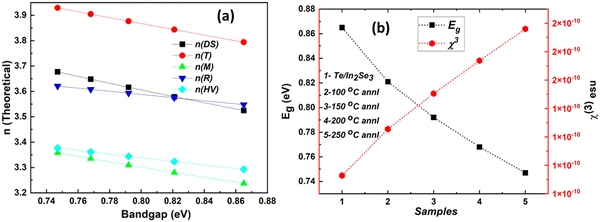
χ(1) is due to the effect of polymerization and homogenization by annealing. It leads to local structural change. The refractive index of a material is related to the nonlinearity, so the susceptibility is changed due to the inclusion of metal into the host matrix. The variation of ‘
Eg’ and
χ(3) for different films is illustrated in
Fig. 10b at different annealing conditions. The Se
85Te
10In
5 film has
χ(1) and
χ(3) values as 0.208 and 0.407 × 10
−12 esu, whereas the present sample shows a higher value, as mentioned in
Table 2.
59 The nonlinear refractive index (
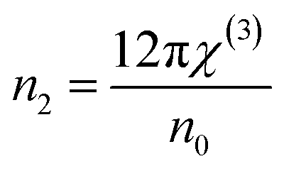
n2) is dependent on the incident ray intensity and ultimately is associated with the
χ(3) value. It is calculated by the relation,
49| |  | (6d) |
The calculated value of ‘n2’ varies from 1.244 × 10⁻⁹ esu to 1.721 × 10⁻⁹ esu for the Te/In2Se3 film and 250 °C annealed film. The obtained n2 and χ(3) values are more as compared to silica, which has potential applications in many nonlinear optical devices.60 The obtained nonlinear parameters of the annealed films are good for various nonlinear optical devices.
3.6. Surface wettability study
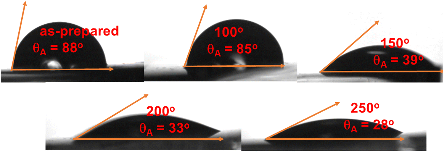
Surface wettability is generally determined by contact angle analysis. It is a function of surface physicochemical properties, including surface functional groups, surface roughness, surface charges, and surface free energy. Contact angle measurement is a simple stand-alone method that provides information on surface tension, hydrophilicity, hydrophobicity, and interaction energy.61 The contact angle is an important surface quantity in determining the wetting capability of the film surface. It is of more importance to surface science for its fundamental aspects and applications. Generally, the nature of the surface is determined by its adhesion related to wetting. The evaluation of the degree of interaction between liquid and solid surfaces in contact measures the surface wettability. Such quantity is evaluated by contact angle measurement, and the measured angle is termed as contact angle (θA). For the surface with high wettability nature, the θA is very small (<90°), and such quality is called a hydrophilic nature. For the surface with low wettability, the contact angle is generally very high (>90°), which is termed a hydrophobic surface.
From Fig. 11, θA = 88°, which shows the hydrophilic nature of the as-prepared film surface. However, upon annealing the Te/In2Se3 film at 100 °C, the θA value was reduced to 85°. There is a gradual decrease in the θA value that infers the increased hydrophilicity by the film surfaces. The 250 °C annealed film shows θA = 28°. So, it can be concluded that the hydrophilicity of the films increases with annealing, therefore increasing surface wettability. Hence, the ability to spread increases as the annealing temperature increases. This is explained by Wenzel's theory, which states that the hydrophilicity of an inherently hydrophilic surface improves when the material is made rougher.62 The surface energy (γse) is evaluated by the equation γse = γw (1 + cosθ)2/4. Here, the surface tension of water, γw = 71.99 mNm−1.63 The ‘γse values for the annealed film increased, as shown in Table 3. It infers an increase in hydrophilicity with annealing. The Young–Dupre's relation, Wsl = γw (1 + cosθ),3 presents the strength of binding between water droplets and solid surfaces. The adhesion between the solid and liquid surfaces is Wsl which is enhanced by annealing (Table 3). The hydrophilic surfaces are helpful for biofilm formation.64 For a super hydrophilic film, the condensed layer of water molecules on the surface reduces the interactions between the surface and bacterial cells. Ivanova et al. showed that the Gram-positive and negative bacteria are killed by the hydrophilic black silicon with nano protrusion. So, the hydrophilicity shown by the higher annealed film can be used for antibacterial activity and the formation of good biofilm. The hydrophilic surfaces are used for biomedical applications. The increase in the wettability of the surface is suitable for manufacturing materials suitable for biomedical applications.65 A super-hydrophilic film surface is effectively used for anti-fogging and self-cleaning applications. The improved hydrophilicity after coating in electrospun nanofiber is useful for filtration applications.66
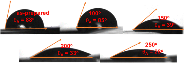 |
| | Fig. 11 Contact angle pictures of Te/In2Se3 thin films. | |
Table 3 Contact angle data of Te/In2Se3 thin films
| Sample |
θ
A (degree) |
γ
se (mN m−1) |
W
sl (mN m−1) |
| Te/In2Se3 |
88 |
19.275 |
74.502 |
| 100 °C |
85 |
21.271 |
78.264 |
| 150 °C |
39 |
56.841 |
127.936 |
| 200 °C |
33 |
60.844 |
132.365 |
| 250 °C |
28 |
63.809 |
135.553 |
3.7. Photo-response study
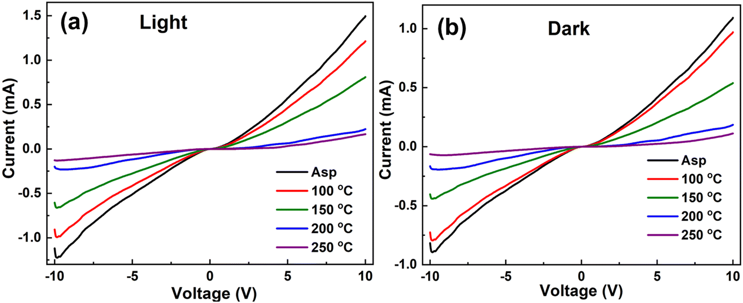
The I–V characteristics of In2Se3, a compound semiconductor, are crucial for understanding its electronic properties and potential applications. When a voltage is applied across a material like In2Se3, the resulting current–voltage relationship can reveal important information about its conductivity, carrier mobility, and other electrical behaviors.67 Typically, the I–V characteristics of In2Se3 exhibit nonlinear behavior, indicating its semiconductor nature. At low voltages, the current rises slowly as carriers begin to overcome the energy barriers present within the material. As the voltage increases, the current increases exponentially, demonstrating the onset of carrier injection and multiplication processes. This exponential increase is characteristic of semiconductor behavior.68 Annealing Te/In2Se3 heterostructures can influence their electronic properties by altering the interface structure, and carrier transport mechanisms.69 In the current case, the illumination light gradually decreased the photocurrent with the increase in the annealing temperature. A similar pattern was also observed for the dark condition. Fig. 12(a and b) represents I–V characteristics at light and dark conditions of the studied thin films.
 |
| | Fig. 12
I–V characteristics plot (a) light and (b) dark for the Te/In2Se3 thin films. | |
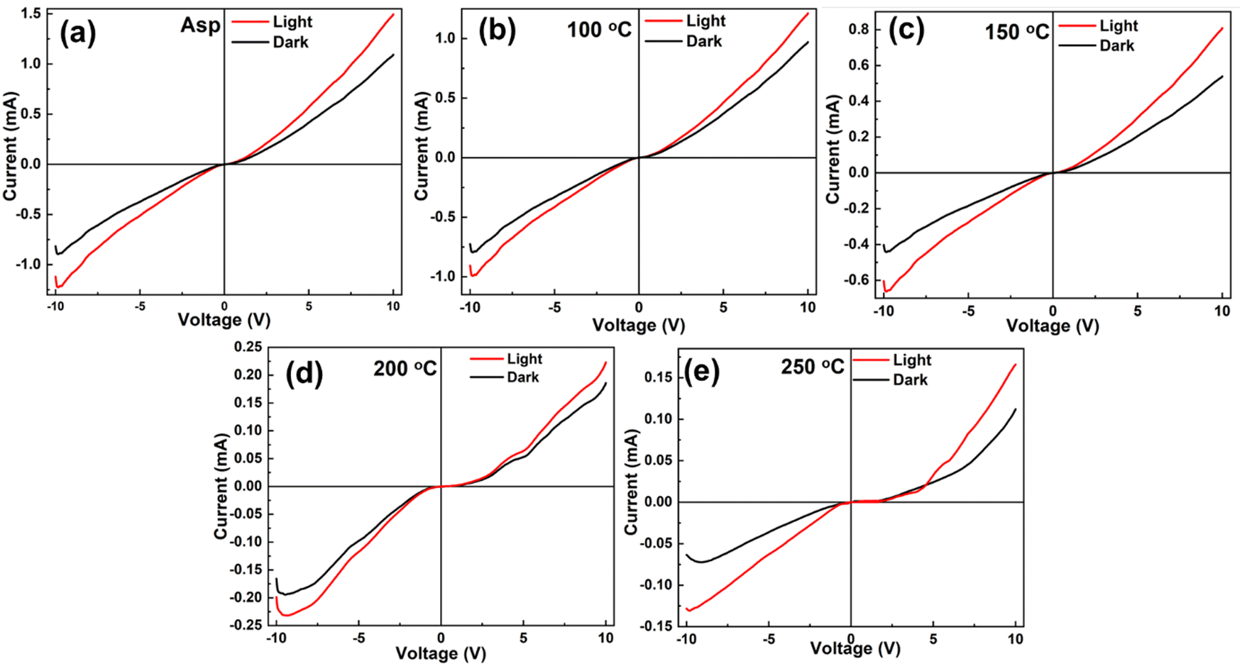
The electrical conductivity is found to have increased with positive applied voltage, and the opposite trend is seen for the negative voltage. The electron migration from the valence to the conducting bands is the root cause of such changes with bias voltage. The curves, which are crossing during the increase and decrease of voltage, could be associated with the defect that disturbs the conducting lines.70 The light current for the as-prepared material remains in the range of mA only. This shows a good photoconductivity of the material. The individual plots for all the investigated films are represented in Fig. 13(a–e). This clearly shows the enhanced light current and decreased dark current for all samples. The resistance of all the films was evaluated from the linear fitting of the I–V curve and taking the inverse of slope (V/I). The values vary from 6.33 kΩ, 7.80 kΩ,11.71 kΩ, 37.52 kΩ, and 41.55 kΩ for the as-prepared and annealed thin films, respectively, as shown in Fig. S6 (ESI†). The increase in the resistance value clearly shows support for the enhanced current values of the as-prepared film.
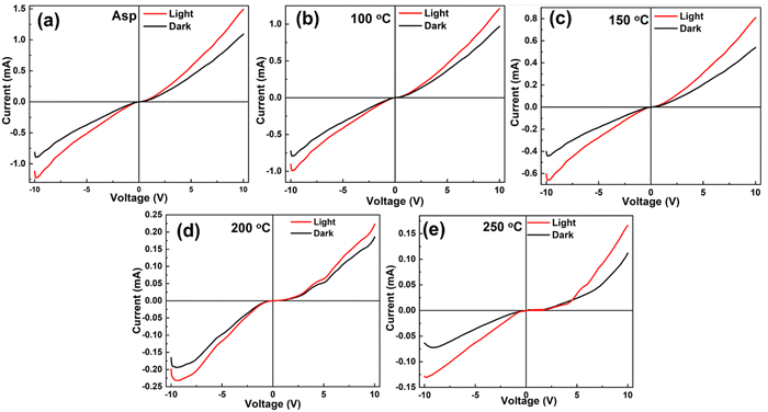 |
| | Fig. 13 Individual I–V characteristics plot (a) as-prepared, (b) 100 °C, (c) 150 °C, (d) 200 °C, and (e) 250 °C under dark and light conditions of Te/In2Se3 thin films. | |
4. Conclusion
The thermally evaporated Te/In2Se3 bi-layer heterostructure films, upon annealing at different temperatures like 100, 150, 200, and 250 °C, showed prominent changes in their structural, optical, electronic, morphology, and surface wettability properties. The bilayer heterostructure and its intermixing upon annealing were verified from the cross-sectional FESEM view and the surface morphological changes through FESEM images upon annealing. The EDX mapping showed the uniform distribution of the atoms in the films. The increased crystallinity was obtained from the XRD, which showed an increase in average crystallite size from 19.11 nm to 48.54 nm upon annealing. The lattice strain increased, and dislocation density decreased upon annealing. The phases present in the film were identified in the HRTEM study and the microstructural changes were seen through the change in Raman intensity. The significant decrease in transmittance increased the absorbance, optical density, and extinction coefficient while decreasing the skin depth with annealing temperatures. The bandgap reduction by 13.64% upon 250 °C annealing influenced the refractive index, which increased. The change is due to the increase in crystallite size and the density of defect states. The dielectric constant increased with a decrease in optical electronegativity with annealing. The increase in refractive index value increased the 3rd-order nonlinear susceptibility value from 1.164 × 10⁻¹⁰ esu to 1.680 × 10⁻¹⁰ esu. The enhancement in the hydrophilicity of the annealed films is good for biomedical and self-cleaning applications. The annealing-induced modifications in the photocurrent are useful for various optoelectronic applications.
Data availability
The data supporting this article have been included as part of the ESI.† The data are plotted with the help of Origin software. Analysis and quantification of images were performed using ImageJ software. The data will be available on request from the corresponding author.
Conflicts of interest
The authors have no conflicts to disclose.
Acknowledgements
The author, Dr R. Naik, thanks the central instrumentation facility of ICT-IOC for different characterizations.
References
- J. O. Island, S. I. Blanter, M. Buscema, H. S. J. Van Der Zant and A. Castellanos-Gomez, Gate controlled photocurrent generation mechanisms in high-gain In2Se3 phototransistors, Nano Lett., 2015, 15, 7853–7858 CrossRef CAS PubMed.
- P. Priyadarshini, P. C. Kumar and R. Naik, Tuning in optoelectronic properties of In/Te bilayer heterostructure upon annealing at different temperatures: surface wettability and photo response study for photonic and solar cell applications, RSC Adv., 2024, 14, 12897 RSC.
- A. Politano, D. Campi, M. Cattelan, I. Ben Amara, S. Jaziri, A. Mazzotti, A. Barinov, B. Gürbulak, S. Duman, S. Agnoli, L. S. Caputi, G. Granozzi and A. Cupolillo, Indium selenide: an insight into electronic band structure and surface excitations, Sci. Rep., 2017, 7, 1–11 CrossRef CAS.
- W. Feng, W. Zheng, X. Chen, G. Liu, W. Cao and P. Hu, Solid-state reaction synthesis of an InSe/CuInSe2 lateral p–n heterojunction and application in high-performance optoelectronic devices, Chem. Mater., 2015, 27, 983–989 CrossRef CAS.
- M. Emziane and R. Le Ny, Synthesis and properties of In2(Se1−xTex)3 thin films: a new semiconductor compound, Appl. Phys. A: Mater. Sci. Process., 2001, 72, 73–79 CrossRef CAS.
- S. Joshi, J. D. Rodney, A. James, P. K. Behera and N. K. Udayashankar, Investigation of Indium doped Se-Te bulk chalcogenide glasses for electrical switching and phase changing applications, J. Alloys Compd., 2024, 978, 173427 CrossRef CAS.
- A. Goktas, A. Tumbul, Z. Aba and M. Durgun, Mgdoping levels and annealing temperature-induced structural, optical and electrical properties of highly c-axis oriented ZnO:Mg thin films and Al/ZnO:Mg/p-Si/Al heterojunction diode, Thin Solid Films, 2019, 680, 20–30 CrossRef CAS.
- P. Priyadarshini, S. Das and R. Naik, A review on metal-doped chalcogenide films and their effect on various optoelectronic properties for different applications, RSC Adv., 2022, 12, 9599–9620 RSC.
- H. P. Pathak, N. Shukla, V. Kumar and D. K. Dwivedi, Structural and optical properties of in doped Se–Te phase-change thin films: a material for optical data storage, Opt. Mater., 2016, 52, 69–74 CrossRef CAS.
- N. S. Saxena, M. M. Imran and K. Singh, Simultaneous measurements of thermal conductivity and diffusivity of Se80Te20–xInx (x = 2, 4, 6 and 10) chalcogenide glasses at room temperature, Bull. Mater. Sci., 2002, 25, 241–245 CrossRef CAS.
- M. Pandian, A. Krishnaprasanth, M. Palanisamy, G. Bangaru, R. Meena, C.-L. Dong and A. Kandasami, Effects of heavy ion irradiation on the thermoelectric properties of In2(Te1−xSex)3 Thin Films, Nanomaterials, 2022, 12, 3782 CrossRef CAS PubMed.
- S. Giri, P. Priyadarshini, D. Alagarasan, R. Ganesan and R. Naik, Annealing-induced phase transformation in In10Se70Te20 thin films and its structural, optical and morphological changes for optoelectronic applications, RSC Adv., 2023, 13, 24955 RSC.
- J. Shang, L. Pan, X. Wang, J. Li, H. X. Deng and Z. Wei, Tunable electronic and optical properties of InSe/InTe van der Waals heterostructures toward optoelectronic applications, J. Mater. Chem. C, 2018, 6, 7201–7206 RSC.
- P. Mannu, M. Palanisamy, G. Bangaru, S. Ramakrishnan, R. Meena, C.-L. Dong and A. Kandasami, Enhancement of thermoelectric performance of n-type In2(Te0.94Se0.06)3 thin films by electronic excitations, Appl. Surf. Sci., 2020, 505, 144115 CrossRef CAS.
- M. Pandian, P. Matheswaran, B. Gokul, R. Sathyamoorthy and K. Asokan, Structural, optical and electrical properties of In2(Te1−xSex)3 thin films, Vacuum, 2018, 147, 107–114 CrossRef CAS.
- R. Panda, H. Rath, S. A. Khan, D. Alagarasan, U. P. Singh, N. C. Mishra and R. Naik, Interface engineered nanostructured phase formation at Se/In sites by Ag ion irradiation and its structural, optical and morphological behavior, Surf. Interfaces, 2023, 40, 103081 CrossRef CAS.
- Y. Oh, J. Lee and M. Lee, Fabrication of Ag-Au bimetallic nanoparticles by laser-induced dewetting of bilayer films, Appl. Surf. Sci., 2018, 434, 1293–1299 CrossRef CAS.
- M. S. Ebied, A. F. Elhady, M. Dongol and A. A. Abuelwafa, Thermal annealing induced modification in linear and nonlinear optical properties of Ag/Ge20Se50S30 bilayer film, Opt. Mater., 2024, 148, 114962 CrossRef CAS.
- R. Naik, C. Kumar, R. Ganesan and K. S. Sangunni, Effect of Te addition on the optical properties of As2S3 thin film, Mater. Chem. Phys., 2011, 130, 750–754 CrossRef CAS.
- M. Behera, R. Panda and R. Naik, Laser induced Te diffusion in amorphous As50Se50 thin films probed by FTIR and XPS, Ind, J. Phys., 2017, 91, 555–562 CAS.
- A. Goktas, S. Modanli, A. Tumbul and A. Kilic, Facile synthesis and characterization of ZnO, ZnO:Co, and ZnO/ZnO:Co nano rod-like homojunction thin films: Role of crystallite/grain size and microstrain in photocatalytic performance, J. Alloys Compd., 2022, 893, 162334 CrossRef CAS.
- Z. K. Kadhama and S. A. Hussain, Impact of the annealing temperature on the structural, morphology and optical properties of bilayer thin films In/Se prepared by thermal evaporation method, Chalcogen. Lett., 2022, 19, 673–681 CrossRef.
- P. Priyadarshini, D. Sahoo, D. Alagarasan, R. Ganesan, S. Varadharajaperumal and R. Naik, Structural and optoelectronic properties change in Bi/In2Se3 heterostructure films by thermal annealing and laser irradiation, J. Appl. Phys., 2021, 129, 223101 CrossRef CAS.
- R. Panda, M. Panda, H. Rath, U. P. Singh, R. Naik and N. C. Mishra, Annealing induced AgInSe2 formation from Ag/In/Ag/In multilayer film for solar cell absorbing layer, Opt. Mater., 2018, 84, 618–624 CrossRef CAS.
- Y. Jia, H. Cheng, J. Qiu, F. Han, Y. Zou, Z. Li, X. Zhou and H. Xu, Effect of temperature on diffusion behavior of Te into nickel, J. Nucl. Mater., 2013, 441, 372–379 CrossRef CAS.
- J. P. Enríquez, E. G. Barojas, R. S. González and U. Pal, S and Te inter-diffusion in CdTe/CdS heterojunction, Sol. Energy Mater. Sol. Cells, 2007, 91, 1392–1397 CrossRef.
- B. E. McCandless, L. V. Moulton and R. W. Birkmire, Recrystallization and sulfur diffusion in CdCl2-treated CdTe/CdS thin films, Prog. Photovoltaics, 1997, 5, 249 CAS.
- S. Das, S. Senapati, D. Alagarasan, S. Varadhrajaperumal, R. Ganesan and R. Naik, Thermal Annealing-Induced Transformation of Structural, Morphological, Linear, and Nonlinear Optical Parameters of Quaternary As20Ag10Te10Se60 Thin Films for Optical Applications, ACS Appl. Opt. Mater., 2023, 1, 17–31 CrossRef CAS.
- A. Goktas, E. Aslan, F. Arslan and A. Kilic, Characterization of multifunctional solution-processed Sn1−xZnxS nanostructured thin films for photosensitivity and photocatalytic applications, Opt. Mater., 2022, 133, 112984 CrossRef CAS.
- Z. Aba, A. Goktas and A. Kilic, Characterization of Zn1−xLaxS thin films; compositional, surface, optical, and photoluminescence properties for possible optoelectronic and photocatalytic applications, J. Sol-Gel Sci. Technol., 2024, 109, 260–271 CrossRef CAS.
- H. T. El-Shair and A. E. Bekheet, Effect of heat treatment on the optical properties of In2Se3 thin films, J. Phys. D: Appl. Phys., 1992, 25, 1122–1130 CrossRef CAS.
- E. Aslan, G. Sahin and A. Goktas, Facile synthesis of Sb2S3 micro-materials for highly sensitive visible light photodetectors and photocatalytic applications, Mater. Chem. Phys., 2023, 307, 128160 CrossRef CAS.
- F. Mikailzade, F. Önal, M. Maksutoglu, M. Zarbali and A. Göktaş, Structure and Magnetization of Polycrystalline La0.66Ca0.33MnO3 and La0.66Ba0.33MnO3 Films Prepared Using Sol-Gel Technique, J. Supercond. Nov. Magn., 2018, 31, 4141–4145 CrossRef CAS.
- P. Wyzga, S. Grimm, V. Garbe, E. Z. Puelles, C. Himcinschi, I. Veremchuk, A. L. Jasper and R. Gumeniuk, Improving thermoelectric performance of indium thiospinel by Se- and Te-substitution, J. Mater. Chem. C, 2021, 9, 4008–4019 RSC.
- C. Liu, Y. Yuan, X. Zhang, J. Su, X. Song, H. Ling, Y. Liao, H. Zhang, Y. Zheng and J. Li, Ta Doping Effect on Structural and Optical Properties of InTe Thin Films, Nanomaterials, 2020, 10, 1887 CrossRef CAS.
- M. R. Molas, A. V. Tyurnina, V. Zólyomi, A. K. Ott, D. J. Terry, M. J. Hamer, C. Yelgel, A. Babinski, A. G. Nasibulin, A. C. Ferrari, V. I. Falko and R. Gorbachev, Raman spectroscopy of GaSe and InSe post-transition metal chalcogenides layers, Faraday Discuss., 2021, 227, 163–170 RSC.
- K. C. Demir, E. Demir, S. Yuksel and C. Coskun, Influence of deposition conditions on nanostructured InSe thin films, Curr. Appl. Phys., 2019, 19, 1404–1413 CrossRef.
- I. N. Reddy, C. V. Reddy, M. Cho, J. Shim and D. Kim, Structural, optical and XPS study of thermal evaporated In2O3 thin films, Mater. Res. Express, 2017, 4, 086406 CrossRef.
- D. Sahoo, P. Priyadarshini, A. Aparimita, D. Alagarasan, R. Ganesan, S. Varadharajaperumal and R. Naik, Optimization of linear and nonlinear optical parameters of As40Se50Te10 thin films by thermal annealing, Opt. Laser Technol., 2021, 140, 107036 CrossRef CAS.
- M. Peng, R. Xie, Z. Wang, P. Wang, F. Wang, H. Ge, Y. Wang, F. Zhong, P. Wu, J. Ye, Q. Li, L. Zhang, X. Ge, Y. Ye, Y. Lei, W. Jiang, Z. Hu, F. Wu, X. Zhou, J. Miao, J. Wang, H. Yan, C. Shan, J. Dai, C. Chen, X. Chen, W. Lu and W. Hu, Blackbody-sensitive room-temperature infrared photodetectors based on low-dimensional tellurium grown by chemical vapor deposition, Sci. Adv., 2021, 7, eabf7358 CrossRef CAS PubMed.
- R. Naik, S. Jena, R. Ganesan and N. K. Sahoo, Laser-induced optical properties change in Sb10 S40Se50 chalcogenide thin films: An investigation through FTIR and XPS measurements, Phys. Status Solidi B, 2014, 251, 661–668 CrossRef CAS.
- A. A. Al-Ghamdi, S. A. Khan, S. Al-Heniti, F. A. Al-Agel and M. Zulfequar, Annealing and laser irradiation effects on optical constants of Ga15Se85 and Ga15Se83In2 chalcogenide thin films, Curr. Appl. Phys., 2011, 11, 315–320 CrossRef.
- M. S. Ebied, A. F. Elhady, M. Dongol and A. A. Abuelwafa, Thermal annealing induced modification in linear and nonlinear optical properties of Ag/Ge20Se50S30 bilayer film, Opt. Mater., 2024, 148, 114962 CrossRef CAS.
- A. A. A. Darwish, Shams A. M. Issab and M. M. El-Nahass, Effect of gamma irradiation on structural, electrical and optical properties of nanostructure thin films of nickel phthalocyanine, Synth. Met., 2016, 215, 200–206 CrossRef CAS.
- D. Biswas, R. Mondal, D. Mandal and S. Mondal, Investigation on Bi-induced changes on linear and non-linear optical parameters of As45Se(55−x)Bix chalcogenide glasses for photonic application, J. Non-Cryst. Solids, 2023, 614, 122401 CrossRef CAS.
-
J. Tauc, in Amorphous and Liquid Semiconductors, ed. J. Tauc, Plenum Press, London and New York, 1974 Search PubMed.
- S. D. Chavhan, S. Senthilarasu and S. H. Lee, Annealing effect on the structural and optical properties of a Cd1− xZnxS thin film for photovoltaic applications, Appl. Surf. Sci., 2008, 254, 4539 CrossRef CAS.
- M. Sadeq, T. Elmosalami and M. Abdo, Induced linear and nonlinear optical modifications of nickel-cadmium borosilicate glass by sunlight irradiation, Ceram. Int., 2022, 48, 34610–34616 CrossRef CAS.
- V. Dimitrov and S. Sakka, Linear and nonlinear optical properties of simple oxides. II, J. Appl. Phys., 1996, 79, 1741–1745 CrossRef CAS.
- T. S. Moss, A relationship between the refractive index and the infra-red threshold of sensitivity for photoconductors, Proc. Phys. Soc., London, Sect. B, 1950, 63, 167–176 CrossRef.
- N. M. Ravindra, S. Auluck and V. K. Srivastava, On the penn gap in semiconductors, Phys. Status Solidi B, 1979, 93, 155–160 CrossRef.
- P. Herve and L. K. J. Vandamme, General relation between refractive index and energy gap in semiconductors, Infrared Phys. Technol., 1994, 35, 609–615 CrossRef CAS.
- S. K. Tripathy, Refractive indices of semiconductors from energy gaps, Opt. Mater., 2015, 46, 240–246 CrossRef CAS.
- J. A. Duffy, Trends in energy gaps of binary compounds: an approach based upon electron transfer parameters from optical spectroscopy, J. Phys. C-Solid State Phys., 1980, 13, 2979 CrossRef CAS.
- I. Chung and M. G. Kanatzidis, Metal Chalcogenides: A rich source of nonlinear optical materials, Chem. Mater., 2014, 26, 849–869 CrossRef CAS.
- D. Sahoo, S. Sahoo, D. Alagarasan, R. Ganesan, S. Varadharajaperumal and R. Naik, Proton ion irradiation on As40Se50Sb10 thin films: Fluence-dependent tuning of linear–non-linear optical properties for photonic applications, ACS Appl. Electron. Mater., 2022, 4, 856–868 CrossRef CAS.
- A. A. Abuelwafa, A. E. Denglawey, M. Dongol, M. M. E. Nahass and T. Soga, Influence of annealing temperature on structural and optical properties of nanocrystalline Platinum octaethylporphyrin (PtOEP) thin films, Opt. Mater., 2015, 49, 271–278 CrossRef CAS.
- H. Ticha and L. Tichy, Semiempirical relation between nonlinear susceptibility (refractive index), linear refractive index and optical gap and its application to amorphous chalcogenides, J. Optoelectron., Adv. Mater., 2002, 4, 381–386 CAS.
- L. K. Benjamin, P. Dube, C. B. Tabi and C. M. Muiva, Physical, linear and nonlinear optical properties of amorphous Se90−xTe10Mx (M = Zn, In, Pb, x = 0, 5) chalcogenide thin films by electron-beam deposition, J. Non-Cryst. Solids, 2021, 557, 120646 Search PubMed.
- X. Duan and Y. Jiang, Annealing effects on the structural and electrical transport properties of n-type Bi2Te2.7Se0.3 thin films deposited by flash evaporation, Appl. Surf. Sci., 2010, 256, 7365–7370 Search PubMed.
- M. F. Ismail, M. A. Islam, B. Khorshidi, A. T. Bagha and M. Sadrzadeh, Surface characterization of thin-film composite membranes using contact angle technique: Review of quantification strategies and applications, Adv. Colloid Interface Sci., 2022, 299, 102524 Search PubMed.
- S. V. Oopath, A. Baji, M. Abtahi, T. Q. Luu, K. Vasilev and V. K. Truong, Nature-Inspired Biomimetic Surfaces for Controlling Bacterial Attachment and Biofilm Development, Adv. Mater. Interfaces, 2023, 10, 2201425 Search PubMed.
- S. Giri, P. Priyadarshini, D. Alagarasan, R. Ganesan and R. Naik, Influence of Te replacement by Bi in In10Se70Te20−xBix films and its structural, optical, morphological, surface wettability and thermal behaviors for optoelectronic applications, Opt. Mater., 2023, 146, 114522 CrossRef CAS.
- P. Tang, W. Zhang, Y. Wang, B. Zhang, H. Wang, C. Lin and L. Zhang, Effect of Superhydrophobic Surface of Titanium on Staphylococcus aureus Adhesion, J. Nanomater., 2011, 2011, 178921 Search PubMed.
- M. Gosecka and T. Basinska, Hydrophilic polymers grafted surfaces: preparation, characterization, and biomedical applications. Achievements and challenges, Polym. Adv. Technol., 2015, 26, 696–706 CrossRef CAS.
- L. Huang, J. T. Arena, S. S. Manickam, X. Jiang, B. G. Willis and J. R. McCutcheon, Improved mechanical properties and hydrophilicity of electrospun nanofiber membranes for filtration applications by dopamine modification, J. Membr. Sci., 2014, 460, 241–249 CrossRef CAS.
- W. Cai, J. Wang, Y. He, S. Liu, Q. Xiong, Z. Liu and Q. Zhang, Strain-modulated photoelectric responses from a flexible α-In2Se3/3R MoS2 heterojunction, Nanomicro Lett., 2021, 13, 74 Search PubMed.
- Y. Hase, V. Sharma, M. Prasad, R. Aher, S. Shah, V. Doiphode, A. Waghmare, A. Punde, P. Shinde, S. Rahane and B. Bade, Fabrication of γ-In2Se3 based photodetector using RF magnetron sputtering and investigations of its temperature-dependent properties, IEEE Sens. J., 2023, 23, 5681–5694 CAS.
- Chanchal, K. Jindal, A. Pandey, M. Tomar and P. K. Jha, Phase-defined growth of In2Se3 thin films using PLD technique for high performance self-powered UV photodetector, Appl. Surf. Sci., 2022, 595, 153505 CrossRef CAS.
- A. F. Kraidy, I. M. E. Radaf, A. Zeinert, A. Lahmar, A. P. Barranco and Y. Gagou, Optoelectrical properties of the ternary chalcogenide SnSb2S5 as a new absorber layer for photovoltaic application, J. Phys. D: Appl. Phys., 2024, 57, 205102 Search PubMed.
|
| This journal is © The Royal Society of Chemistry 2025 |
Click here to see how this site uses Cookies. View our privacy policy here. 
 Open Access Article
 This Open Access Article is licensed under a Creative Commons Attribution-Non Commercial 3.0 Unported Licence
 a,
D.
Alagarasan
b and
R.
Naik
a,
D.
Alagarasan
b and
R.
Naik


 . The macro strain-induced XRD peak broadening is given by βstrain = 4ε

 value varies with annealing temperature in an increased pattern, as shown in Fig. 8(c). The presence of high amounts of unsaturated bonds and defects in the chalcogenide material, are accountable for localized states. The heating of the films annealed out those unsaturated defects and created more saturated bonds. The localized state density is reduced by the decreased concentration of unsaturated defects, which affects the refractive index (n) and k values. The increase in ‘k’ with annealing is because of the change in density as ‘k’ is related to surface defects and disorder, which arise from Te diffusion into the In2Se3 layer.43

 , with A = 25.54 gives information about the attractiveness of a radical or atom to electrons to form an ionic bond. The evaluated values gradually decrease from 1.640 (as-prepared) to 1.623 upon annealing at 250 °C (Table 2). The small change of 1.03% shows the stability of the annealed films on optical electronegativity.
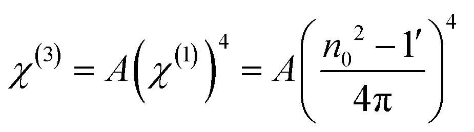
 and ‘A’ = ∼1.7 × 10⁻¹⁰. The obtained values of ‘χ(1)’ and ‘χ(3)’ using static refractive index are presented in Table 2. It is observed that the as-prepared Te/In2Se3 film possesses ‘χ(3)’ as 1.164 × 10⁻¹⁰ esu, which increased to 1.68 × 10⁻¹⁰ esu for the 250 °C annealed film. Such change is due to enhancement in ‘χ(1)’ on annealing. The increase in χ(3) and χ(1) is due to the effect of polymerization and homogenization by annealing. It leads to local structural change. The refractive index of a material is related to the nonlinearity, so the susceptibility is changed due to the inclusion of metal into the host matrix. The variation of ‘Eg’ and χ(3) for different films is illustrated in Fig. 10b at different annealing conditions. The Se85Te10In5 film has χ(1) and χ(3) values as 0.208 and 0.407 × 10⁻¹² esu, whereas the present sample shows a higher value, as mentioned in Table 2.59 The nonlinear refractive index (n2) is dependent on the incident ray intensity and ultimately is associated with the χ(3) value. It is calculated by the relation,49