
 Open Access Article
 This Open Access Article is licensed under a Creative Commons Attribution-Non Commercial 3.0 Unported Licence
Enhanced transport, dielectric and magnetic properties of Ni-doped (YFeO3)0.5(BaTiO3)0.5 perovskite for NTC thermistor and multifunctional applications
Harshavardhan
Chouhan
a,
Saurabh
Prasad
a,
B. N.
Parida
a and
R. K.
Parida
 *b
*b
aDepartment of Physics, Central Institute of Technology Kokrajhar (Deemed to be University, MoE, Govt. of India), BTR, Assam 783370, India. E-mail: rkparida65@gmail.com; bnparida@cit.ac.in
bDepartment of Physics, Siksha ‘O’ Anusandhan (Deemed to be University), Khandigiri, Bhubaneswar, Odisha 751030, India
First published on 4th June 2025
Abstract
The solid-state reaction method was successfully employed to synthesize the environmentally friendly polycrystalline perovskite (Y0.5Ni0.5FeO3)0.5(BaTiO3)0.5. X-ray diffraction (XRD) analysis, complemented by Rietveld refinement, confirms its multiphase crystalline structure, comprising two cubic and one orthorhombic phase. Field-emission scanning electron microscopy (FE-SEM) reveals a well-defined surface morphology, while energy-dispersive spectroscopy (EDS) and elemental mapping validate the homogeneous distribution of constituent elements. Raman and FTIR spectroscopy further confirm the vibrational and atomic structural integrity of the material. Dielectric studies indicate a high dielectric constant (∼338 at 100 Hz, room temperature), with strong frequency and temperature-dependent relaxation effects. Impedance spectroscopy reveals non-Debye relaxation behaviour, NTCR characteristics and impedance in the megaohm range at lower temperatures. AC conductivity results align well with Jonscher's power law. The thermistor coefficient (β) reaches 4778.61 at 450 °C, demonstrating excellent potential for thermistor applications. Magnetic studies confirm a prominent ferromagnetic response at room temperature, with a saturation magnetization of 3.654 emu g−1 and coercive field of 196.4 Oe. These combined properties make (Y0.5Ni0.5FeO3)0.5(BaTiO3)0.5 a promising candidate for multifunctional applications.
1. Introduction
Magnetoelectric composite ceramics, which combine both dielectric and magnetic properties, have gained significant attention for their potential use in multifunctional devices such as miniaturized filters, antennas, and electromagnetic interference shielding.1–3 These materials rely on magnetoelectric coupling and offer immense promise for advanced technological applications. Notable examples include the BaTiO3–(MnZn)Fe2O4, BaTiO3–YFeO3 system, which demonstrates high capacitance and static permeability and Ba0.8Sr0.2TiO3/YFeO3 composites that exhibit exceptional permittivity and high saturation magnetization.4–6 However, traditional solid-state methods used to synthesize these materials often require elevated sintering temperatures, which can lead to undesirable diffusion between the dielectric and magnetic phases, resulting in performance degradation and increased grain size.4YFeO3 exists in two distinct polymorphic forms: an orthorhombic perovskite-type structure and a hexagonal structure. The orthorhombic phase, which crystallizes in the Pnma space group, is the more stable and widely studied form, exhibiting G-type antiferromagnetism. Its magnetic properties are derived from Fe3+ ions at the octahedral sites, surrounded by six neighbouring magnetic ions arranged in FeO6 octahedra. The weak ferromagnetism observed in YFeO3 is the result of a canted antiferromagnetic ordering, driven by superexchange interactions between Fe3+–O–Fe2+ bonds and the Dzyaloshinskii–Moriya (DM) interaction. YFeO3has a high Néel temperature (370 °C) and a low Curie temperature (−256 °C), further emphasizing its potential as a robust material for room-temperature applications.7,8 Orthorhombic YFeO3 in addition to its magnetic properties, displays interesting dielectric and electrical properties, including ferroelectricity, which is mainly attributed to structural distortions within the perovskite framework. The presence of Fe3+ ions contributes to charge transfer between Fe2+ and Fe3+ states, which in turn induces dielectric polarization via the Wagner space charge effect. The dielectric relaxation behaviour observed in YFeO3 is due to the movement of charge carriers between these iron states. As a result, YFeO3 is of interest for potential applications in memory storage, sensors and other electronic devices.9,10 The hexagonal phase of YFeO3, while offering superior photocatalytic properties and a smaller optical bandgap (∼1.96 eV), is much more challenging to synthesize and stabilize.11 The transformation from the hexagonal to the orthorhombic phase typically occurs at higher calcination temperatures, limiting the feasibility of obtaining a pure hexagonal phase. Previous research suggests that the hexagonal phase can only be achieved within a very narrow temperature range (700–720 °C) using the sol–gel method, with coexisting minor phases such as Y2O3 or Fe2O3, further complicating its synthesis.11–13 YFeO3, like other rare-earth orthoferrites (RFeO3), has been the focus of extensive research due to its potential applications in magneto-optical devices, including optical switches, magnetic field sensors and current sensors. The magneto-electric coupling in YFeO3, although weak, is significant enough to offer utility in these applications. Recent advances in materials science have led to the development of methods for improving the multiferroic properties of YFeO3 through ion substitution or doping. By substituting elements into the A-site (Y3+) or B-site (Fe3+) of the perovskite structure, it is possible to tune and enhance the material's dielectric, magnetic, and ferroelectric properties.14,15
Several studies have reported on the effects of different dopants on the properties of YFeO3. For instance, doping with Ca2+ in place of Y3+ has been shown to enhance electrical conductivity by creating hole localization on the Fe site to compensate for the charge difference between Ca2+ and Y3+.16 Similarly, doping with magnetic ions such as Gd3+ has been found to enhance magnetic behaviour due to additional Gd–Fe interactions and structural distortions. Other dopants, such as Zn, Cd, Cr, and Lu, have also been investigated, yielding modifications in both magnetic and dielectric properties.17–19 A critical aspect of enhancing the multiferroic properties of YFeO3 involves careful control over the doping concentration. For example, the introduction of Er3+ at low concentrations improves magnetic properties, but at higher concentrations, the material shifts from weak ferromagnetism to paramagnetic behaviour.20 On the other hand, B-site doping of Fe3+ with elements like Mn3+ has been found to reduce relative permittivity and contribute to dielectric relaxation processes, which are influenced by oxygen vacancies within the material.21 Moreover, recent research has focused on the substitution of Nd3+ ions into the A-site of YFeO3. This substitution has been found to enhance the dielectric properties of YFeO3 ceramics, particularly at high frequencies. Substituting Nd3+ does not cause any structural transformation but does influence the overall polarization and electrical behaviour, suggesting potential applications in high-frequency devices. The introduction of rare-earth ions like Nd3+, with different ionic radii compared to Y3+, is an effective strategy for tuning the ferroelectric and ferromagnetic properties of YFeO3 without compromising its structural integrity.17
In addition to magnetic and dielectric properties, YFeO3 exhibits ferroelectric behaviour, although weak. The weak polarization observed in YFeO3 provides a gap in the research, offering opportunities for further study and improvement. The challenge remains to enhance the ferroelectric properties while maintaining the material's multiferroic nature. Given the complex interplay between its magnetic and electric orders, YFeO3 offers a fertile ground for exploring novel approaches to material design and functionality.17,22,23
The integration of YFeO3 with BaTiO3 results in a material with enhanced multiferroic properties, combining strong magnetic and dielectric behaviour. Introducing Ni ions into the YFeO3 lattice further improves these properties. For instance, in the nanostructured YFe1−xNixO3 system (x = 0.1, 0.15, 0.2, 0.25), prepared via co-precipitation and annealed at 800 °C. Magnetic measurements showed that Ni doping significantly increased the material's magnetic properties compared to pure YFeO3. As the Ni content increased from x = 0.1 to 0.25, the coercivity (Hc) decreased from 1332.6 Oe to 887.8 Oe, while the saturation magnetization (Ms) rose from 0.67 to 1.17 emu g−1.24 Furthermore, studies on the YMn0.4Fe0.6−xNixO3 system (x = 0, 0.05, 0.075, 0.1), synthesized using the sol–gel process, showed DC conductivity of all samples followed the same trend as grain size, displaying semiconductor behaviour. Similarly, AC conductivity aligned with DC results, indicating that the non-overlapping small polaron tunneling (NSPT) model governs conduction in this multiferroic system.25 Impedance spectroscopy revealed the contributions of both grain and grain boundaries to the overall conduction process, further supported by Nyquist plots. Among the samples, YMn0.4Fe0.525Ni0.075 O3 demonstrated the highest conductivity, indicating that Ni substitution effectively enhances both electrical and magnetic properties in YFeO3-based materials. This demonstrates the potential of Ni-doped YFeO3 for enhanced magnetic performance.
BaTiO3 (BTO) is a well-established perovskite material, known for its excellent dielectric, piezoelectric, ferroelectric, and electro-optic properties. It finds widespread use in electronic components such as multilayer ceramic capacitors due to its high dielectric constant and thermal stability. On the other hand, YFeO3 (YFO) exhibits notable magnetic and dielectric behaviour, including weak ferroelectricity and G-type antiferromagnetism, primarily due to structural distortions and charge transfer within its orthorhombic perovskite framework. However, the inherent magnetoelectric coupling in pristine YFO remains limited, and efforts to enhance its multifunctional properties have become increasingly vital for applications in sensors, memory devices, and multifunctional electronics.
In this context, the substitution of Ni into the YFO lattice is a key innovation of our work. Ni doping enhances magnetic characteristics such as increasing saturation magnetization (Ms) and modifying coercivity (Hc). By integrating (Y0.5Ni0.5FeO3)0.5 with (BaTiO3)0.5, we have designed a new multiferroic composite that uniquely combines the enhanced magnetic behaviour of Ni-substituted YFO with the high permittivity and ferroelectric features of BTO.
This specific 50–50 composite composition has not been previously reported in the literature and demonstrates a synergistic improvement in both dielectric and magnetic performance. Furthermore, the material's temperature-dependent dielectric behaviour, electrical conductivity, and impedance responses suggest suitability for advanced multifunctional applications, including NTC thermistors, energy storage devices, and magneto-electric sensors. We believe the structural tuning through Ni substitution and the strategic integration with BTO bring genuine novelty to this study and offer a promising pathway toward next-generation multifunctional ceramics.
2. Experimental section
2.1 Preparation of material
We synthesized the sample (Y0.5Ni0.5FeO3)0.5(BaTiO3)0.5 using the conventional solid-state route, employing high-purity BaCO3, Fe2O3, Y2O3, TiO2 and Ni2O3 powders in precise proportions. We carefully weighed these powders according to stoichiometric requirements and blended them thoroughly using an agate mortar and pestle at room temperature to ensure homogeneity. The mixture was ground in both dry and wet conditions for 2 hours each, achieving a uniform admixture. The resulting powder underwent calcination in a programmable furnace, where it was heated gradually to 1200 °C and held for 4 hours. Afterward, we rigorously ground the calcined powder to obtain a lump-free consistency. We then formed cylindrical pellets by pelletizing the calcined material with polyvinyl alcohol (PVA) as a temporary binder. Finally, these pellets were sintered at 1300 °C for 3 hours to densify the sample and eliminate impurities, producing the final specimen.2.2 Characterization of the material
Instrument specifications. Rigaku Ultima IV diffractometer with CuKα radiation (wavelength 1.5418 Å), 2θ range of 20°–90° with a step size of 0.02°.
Instrument specifications. Carl Zeiss Gemini 300 FE-SEM with a magnification scale of 200 nm.
Instrument specifications. Advanced EDS system integrated with FE-SEM for elemental analysis and color mapping.
Instrument Specifications. Horiba Jobin Yvon LabRam HR laser Micro Raman spectrometer for vibrational modes and functional group analysis in the range from 150 cm−1 to 800 cm−1.
Instrument Specifications. PerkinElmer FRONTIER IR and SPECTRUM 100 models for vibrational characteristic analysis in the range from 400 cm−1 to 4000 cm−1.
Instrument specifications. PSM-1735 LCR meter (Newtons4th Ltd, UK) operating in the frequency range of 100 Hz to 106 Hz and temperature range of 25 °C to 500 °C.
Instrument specifications. Keithley electrometer with a temperature range of 50 °C to 450 °C and operating range of −100 to 100 Volts.
Instrument specifications. Microsense ADE-EV9 vibrating sample magnetometer (VSM) with a magnetic field range of −2 T to +2 T, performed at room temperature.
3. Results and discussion
3.1 Crystal structure
A good understanding of a material's crystal structure is required to comprehend its complexity and phase transitions. X-ray elastic scattering is utilized to collect crucial crystal information such as defects, unit cell size, strain, chemical structure and so on. Fig. 1(a) (marked by red dots) shows the X-ray diffraction intensity pattern for the synthesized sample, with Bragg's angle ranging from 20° to 90° at room temperature. The existence of numerous sharp, narrow, well-defined, and clear diffraction peaks confirms the powdered sample's high crystallinity, signifying an ordered and well-structured arrangement of atoms inside the crystal lattice. The peaks seen in the XRD spectrum are different from those of the raw chemicals, indicating the formation of a new structural arrangement. The synthesized XRD pattern was compared to the reference structure from the Crystallography Open Database using the QualX2 software, revealing that the sample has cubic symmetry and belongs to the Pm![[3 with combining macron]](https://www.rsc.org/images/entities/char_0033_0304.gif) m space group. The presence of additional peaks indicates that other phases are also present in the sample.
m space group. The presence of additional peaks indicates that other phases are also present in the sample.
 | ||
| Fig. 1 (a) Rietveld refined XRD pattern of the investigated sample. (b) Williamson–Hall plot of the investigated sample. | ||
Rietveld refinement is an effective method for analyzing the structure of ceramic samples, allowing for accurate measurement of lattice parameter variations. The data shown in Fig. 1(a) were generated using the Full-Prof software, which systematically and sequentially refined various parameters during the process. These parameters consists of background correction, scale factors, peak shapes, cell parameters, instrument zero-point, FWHM parameters, and individual atomic thermal and occupancy properties. The red circles in Fig. 1(a) represents experimental data, while the black lines represents refined data. The green vertical lines on the graph highlight the locations where the allowed Bragg diffraction peaks occur. Below these, the lower lines illustrate the difference between the intensities predicted by the software, shown as solid blue lines and the actual measured intensities from the experiment. Using cod database code 210![[thin space (1/6-em)]](https://www.rsc.org/images/entities/char_2009.gif) 0862 of space group ‘Pmm’, cod database code 2003125 of space group Pnma and cod database code 2300616 of space group Fdm obtained from Crystallography Open Database the refinement is employed. The initial refinement, which considered only a cubic phase with the space group ‘Pmm’, was insufficient to account for all the observed peaks. However, by incorporating both orthorhombic and cubic phases with the space groups ‘Pnma’ and ‘Fdm’, the data fitting significantly improved, resulting in a lower value of χ2 and a more accurate match to the experimental results. The analysis of the data indicates that the cubic phase with the space group Pmm accounts for 76.94% of the total composition, while the orthorhombic phase with the space group Pnma makes up 9.03%, and the cubic phase with the space group Fdm contributes 14.03%. Table 1 presents the refined atomic positions for each phase. The refinement results are further supported by the reliability factors, with Rp(%) at 4.02, Rwp(%) at 5.84, Rexp(%) at 5.1, and χ2 at 1.312. The low value of χ2, along with the alignment of the other reliability parameters, confirms a strong fit with the experimental data. Table 2 displays the refined cell parameters.
0862 of space group ‘Pmm’, cod database code 2003125 of space group Pnma and cod database code 2300616 of space group Fdm obtained from Crystallography Open Database the refinement is employed. The initial refinement, which considered only a cubic phase with the space group ‘Pmm’, was insufficient to account for all the observed peaks. However, by incorporating both orthorhombic and cubic phases with the space groups ‘Pnma’ and ‘Fdm’, the data fitting significantly improved, resulting in a lower value of χ2 and a more accurate match to the experimental results. The analysis of the data indicates that the cubic phase with the space group Pmm accounts for 76.94% of the total composition, while the orthorhombic phase with the space group Pnma makes up 9.03%, and the cubic phase with the space group Fdm contributes 14.03%. Table 1 presents the refined atomic positions for each phase. The refinement results are further supported by the reliability factors, with Rp(%) at 4.02, Rwp(%) at 5.84, Rexp(%) at 5.1, and χ2 at 1.312. The low value of χ2, along with the alignment of the other reliability parameters, confirms a strong fit with the experimental data. Table 2 displays the refined cell parameters.
| Atoms | Phase1 (Pmm) |
||
|---|---|---|---|
| Atomic position | |||
| x | y | z | |
| Ba | 0.5 | 0.5 | 0.5 |
| Ti | 0 | 0 | 0 |
| O | 0.5 | 0 | 0 |
| Y | 0.5 | 0.5 | 0.5 |
| Fe | 0 | 0 | 0 |
| Ni | 0 | 0 | 0 |
| Atoms | Phase2 (Pnma) | ||
|---|---|---|---|
| Atomic position | |||
| x | y | z | |
| Y | 0.07408 | 0.25 | −0.01109 |
| Fe | 0 | 0 | 0.5 |
| O | 0.41927 | 0.25 | 0.09939 |
| O | −0.23468 | −0.0399 | 0.73944 |
| Ba | 0.07408 | 0.25 | −0.01109 |
| Ni | 0 | 0 | 0.5 |
| Ti | 0 | 0 | 0.5 |
| Atoms | Phase 3 (Fdm) |
||
|---|---|---|---|
| Atomic position | |||
| x | y | z | |
| Fe | 0.125 | 0.125 | 0.125 |
| Fe | 0.5 | 0.5 | 0.5 |
| O | 0.24908 | 0.24908 | 0.24908 |
| Parameters | Phase 1 (Pmm) |
Phase 2 (Pnma) | Phase 3 (Fd![[3 with combining macron]](https://www.rsc.org/images/entities/i_char_0033_0304.gif) m) m) |
|
|---|---|---|---|---|
| Cell parameters | a (Å) | 4.004530 | 5.583677 | 8.335494 |
| b (Å) | 4.004530 | 7.600788 | 8.335494 | |
| c (Å) | 4.004530 | 5.281495 | 8.335494 | |
| Cell angle | α | 90 | 90 | 90 |
| β | 90 | 90 | 90 | |
| γ | 90 | 90 | 90 | |
| Reliability factors | R p | 4.02 | ||
| R wp | 5.84 | |||
| R exp | 5.1 | |||
| χ 2 | 1.312 | |||
A detailed analysis of the XRD patterns is conducted using the Williamson–Hall (W–H) plot method. This method is based on an empirical formula, referred to as the Williamson–Hall (W–H) equation, which links two important factors in crystallography: (FWHM) i.e. full width at half maxima, denoted by β, and the lattice strain, symbolized by ε. The equation is expressed as follows:
 | (1) |
In this equation, several variables are involved: k, known as the shape factor, has a value of approximately 0.89; λ represents the wavelength, 1.54 Å for Cu (Kα) radiation; D signifies the average crystallite size; θ is the measured diffraction angle; β corresponds to the full width at half maxima (FWHM); and ε indicates the lattice strain.
The Williamson–Hall plot, shown in Fig. 1(b), depicts the connection between 4sinθ (x-axis) and β![[thin space (1/6-em)]](https://www.rsc.org/images/entities/i_char_2009.gif) cosθ (y-axis), with linear regression applied to analyze the data. By comparing this equation to the standard linear form y = mx + c, the strain values can be calculated. From the analysis, the crystallite size is calculated to be approximately 253.34 nm, while the slope of the graph gives a lattice strain value of 0.000225.
cosθ (y-axis), with linear regression applied to analyze the data. By comparing this equation to the standard linear form y = mx + c, the strain values can be calculated. From the analysis, the crystallite size is calculated to be approximately 253.34 nm, while the slope of the graph gives a lattice strain value of 0.000225.
3.2 Analysis of microstructure and composition
Fig. 2(a) showcases an FE-SEM image of the sample's surface, highlighting its polycrystalline structure with grains of diverse sizes and irregular shapes dispersed unevenly. The micrograph also reveals voids between the grains, which contribute to the hopping mechanism in the material. In Fig. 2(b), a grain size distribution is depicted, calculated using ImageJ software. A Gaussian fit was applied to the histogram data, revealing an average grain size of 225 nm. | ||
| Fig. 2 (a) SEM image of the investigated sample. (b) Histogram mapping for the crystalline size of the investigated sample. (c) EDX spectrum of the investigated sample. (d) The elemental color mapping of the investigated sample, along with the corresponding color mappings of Ti, Ba, O, Y, Fe and Ni individually. | ||
The initial elemental analysis was conducted using energy-dispersive X-ray spectroscopy (EDS). Fig. 2(c) shows the weight percentages of the elements obtained from a specific cross-sectional region of the FESEM micrograph. The EDS spectrum, also illustrated in Fig. 2(c), confirms the presence of the expected elements in the sample, including Ba, Fe, Y, Ni, Ti and O. The absence of any impurity peaks from foreign elements in the spectrum further indicates that the synthesized sample is of high purity. Moreover, Fig. 2(d) presents the color mapping for each of the identified elements within the sample. The absence of any clustering in the images indicates a uniform distribution of these elements across the entire sample.
3.3 Raman spectroscopy
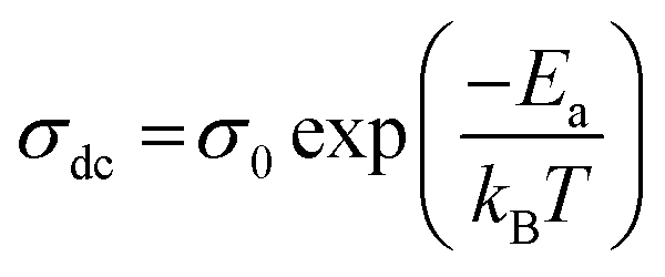
The ambient temperature Raman spectroscopy results for (Y0.5Ni0.5FeO3)0.5(BaTiO3)0.5, as shown in Fig. 3(a), offer valuable insights through a non-destructive technique. From the observed spectra and based on existing literature, we identified seven distinct Raman modes. Specifically, we observed three T2g modes of Ni2FeO4 at 200 cm−1, 481 cm−1, and 564 cm−1, labelled as T2g(I), T2g(II), and T2g(III), respectively; an Eg mode at 325 cm−1; an A1g mode near 700 cm−1; and a B3g mode of YFeO3 at 249 cm−1 and one at 637 cm−1. While cubic BaTiO3 theoretically exhibits no Raman-active modes, the A1g mode of Ni2FeO4, detected around 700 cm−1, is attributed to the symmetrical stretching of metal–oxygen bonds.26 The Eg mode observed at 325 cm−1 corresponds to the symmetric bending of oxygen atoms in relation to cations positioned at tetrahedral sites.27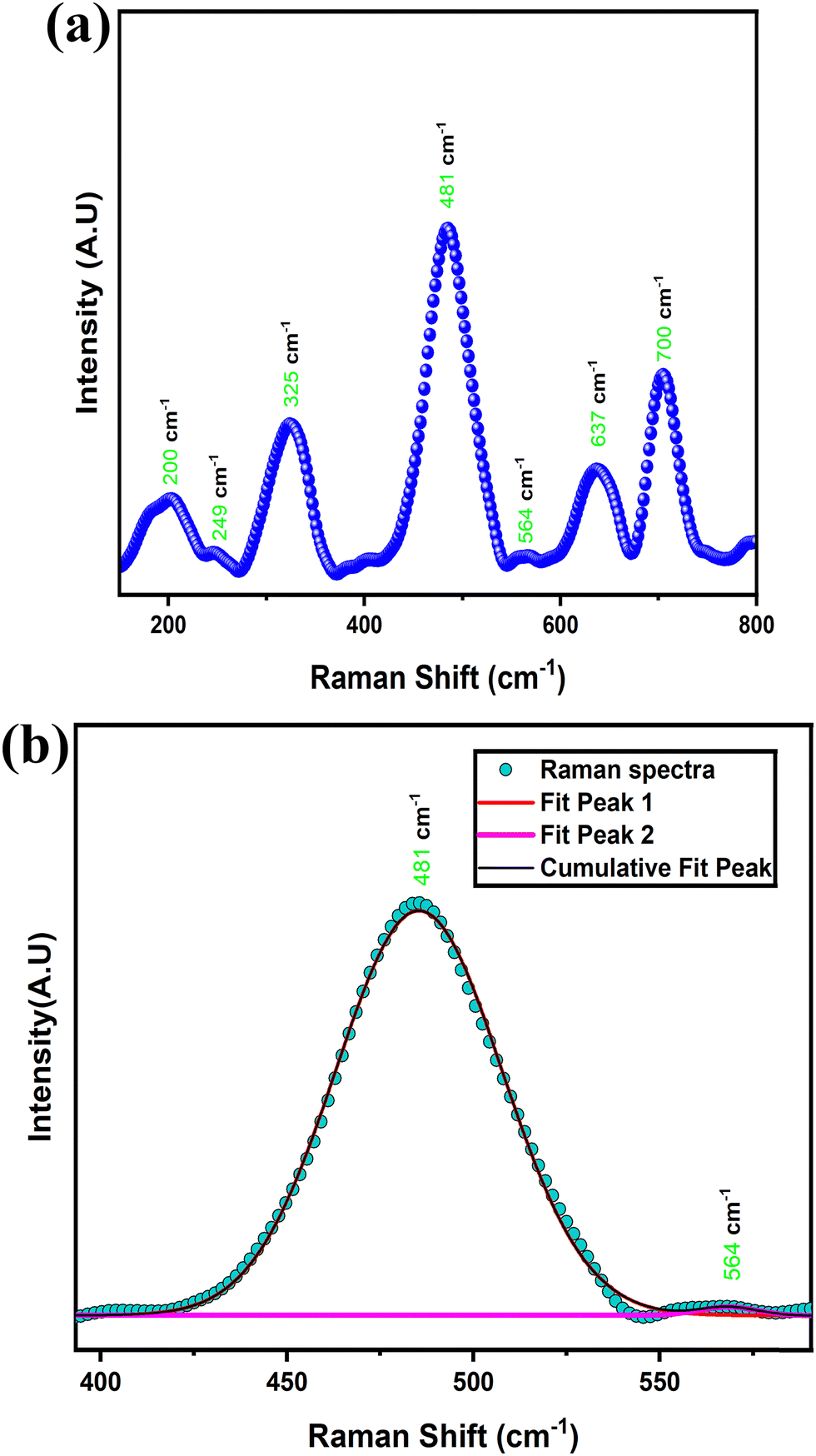 | ||
| Fig. 3 (a) RAMAN spectra of the investigated sample. (b) Deconvolution of RAMAN spectra. | ||
Further examination reveals that the T2g(I) mode at 200 cm−1 and T2g(II) mode at 481 cm−1 represent the asymmetric bending and stretching of the metal–oxygen bonds at octahedral sites, while the T2g(III) mode at 564 cm−1 is linked with the translational movement of the metal–oxygen bonds at tetrahedral sites.27 The closely spaced Raman peaks at approximately 481 cm−1 and 564 cm−1 were resolved by deconvoluting the Raman spectra using a Gaussian fitting model, as shown in Fig. 3(b). As reported by Iliev et al.,28 the B3g mode at 249 cm−1, linked to YFeO3, is a result of Y and O1 atomic motions confined along the y-axis by site symmetry. The peak at 249 cm−1, also observed in YCrO3, reflects the vibration of the yttrium cation.29 Additionally, the prominent broad feature at 637 cm−1 likely originates from a two-phonon process and is possibly due to crystal disorder.30 The Raman spectra reveal that the synthesized sample does not display any Raman-active modes characteristic of the tetragonal phase of BaTiO3. Additionally, based on the literature, it is well-established that the cubic phase of BaTiO3 lacks Raman-active modes. Therefore, we conclude that the sample has undergone a subtle transition to the cubic phase, likely due to the incorporation of BaTiO3 into Ni0.5Y0.5FeO3. This conclusion is well supported by XRD analysis, which confirms the findings from Raman spectroscopy. Together, these results provide useful insights into the structural changes in the sample, enhancing our understanding of its unique properties.
3.4 FTIR spectroscopy
FTIR analysis is employed to verify the atomic fingerprint of the compound. As depicted in Fig. 4, several transmittance peaks were detected within the wavenumber range of 400 cm−1 to 4000 cm−1. A total of eleven distinct peaks were identified at the following wavenumbers: 410 cm−1, 435 cm−1, 451 cm−1, 578 cm−1, 861 cm−1, 1100 cm−1, 1443 cm−1, 1635 cm−1, 2850 cm−1, 2924 cm−1, and 3424 cm−1. | ||
| Fig. 4 FTIR spectra of the investigated sample. | ||
The band at 410 cm−1 is attributed to Ni–O stretching vibrations, while the peak at 435 cm−1 is related to Ti–O bending along the polar axis.31,32 Strong signals at around 451 cm−1 and 578 cm−1 are linked to Fe–O stretching modes within the orthoferrite structure.33 Peaks at 861 cm−1 and 1443 cm−1 are assigned to bending in the COO− group.32 The band at 1100 cm−1 corresponds to C–O vibrations.33 Peaks near 1635 cm−1 and 3424 cm−1 indicate OH stretching and deformation vibrations, while the signals at 2850 cm−1 and 2924 cm−1 are due to symmetric and asymmetric stretching of the –CH2 group, respectively.32–34
3.5 Dielectric studies
The dielectric properties of the synthesized sample were measured over a temperature range of 25–400 °C and a frequency range of 100 Hz to 1 MHz, revealing a frequency and temperature dependent behaviour characteristic. The inset in Fig. 5 shows that the dielectric constant reaches a value of approximately 338 at 100 Hz at room temperature, indicating a high dielectric response at low frequencies. The coexistence of BaTiO3 and YFeO3 strongly affects the material's dielectric properties. BaTiO3 has a high dielectric constant, reaching about 2500 at 25 °C and 100 Hz due to its ferroelectric nature, while YFeO3 has a much lower dielectric constant of around 150 under the same conditions. The measured dielectric constant of 338 at 25 °C and 100 Hz indicates that BaTiO3 significantly enhances the dielectric response, but Ni doped YFeO3 lowers the overall value. The interaction between these two phases, possibly through interfacial effects, further influences the dielectric behaviour, resulting in a dielectric constant lower than pure BaTiO3 but higher than pure YFeO3.35 | ||
Fig. 5 Frequency-dependent dielectric constant  at different temperatures. at different temperatures. | ||
This significant dielectric value can be attributed to multiple polarization mechanisms within the sample, including dipolar, interfacial and space charge polarization effects. The primary dipoles responsible for this response are linked to ionic displacements within the components. Specifically, polar Ti–O and Fe–O bonds contribute to dipolar polarization, while defects, grain boundaries, and interfaces between YNiFeO3 and BaTiO3 phases are likely to create localized charges that produce interfacial and space charge polarizations at lower frequencies.36
As frequency increases, the dielectric constant decreases, ultimately converging around 156 at high frequencies. This reduction in dielectric response with frequency aligns with the theory proposed by Koop and can be explained by the Maxwell–Wagner model for heterogeneous dielectrics.37,38 In this model, the inhomogeneous two-layer structure consists of conducting grains separated by insulating grain boundaries, which act as barriers to the movement of charge carriers. At lower frequencies, the grain boundaries allow charge accumulation, contributing to a high dielectric constant due to space charge polarization. However, as frequency rises, the ability of slower polarization mechanisms, such as interfacial and space charge polarization, to align with the rapidly oscillating electric field diminishes, causing a drop in dielectric constant. In ferrite-based systems, the local hopping of Fe3+ and Fe2+ ions contributes to polarization at lower frequencies. As frequency increases, the Fe3+ ↔ Fe2+ hopping process becomes too slow to follow the field's rapid variations, further reducing εr at higher frequencies.39
With increasing temperature, the dielectric constant also rises notably, reaching a value of approximately 1615 at 100 Hz at 400 °C, as illustrated in Fig. 5. This temperature-induced increase in dielectric constant is primarily due to the activation of thermally sensitive polarization mechanisms. At higher temperatures, thermal energy enhances the mobility of charge carriers and dipoles, facilitating their alignment with the applied field and thus increasing the overall dielectric response. Ionic dipoles, in particular, become more responsive to the electric field as thermal energy overcomes energy barriers to their movement. The increased dielectric response is due to thermally activated space charge polarization, mainly at the boundaries and interfaces of the sample, where charges move more freely at higher temperatures. These effects are more noticeable at low frequencies, as slower polarization mechanisms, like space charge effects, have more time to react, leading to a higher dielectric constant at elevated temperatures.40,41
Across all measured temperatures, the dielectric constant exhibits a similar frequency dependent decrease, converging around 160 at higher frequencies. This consistent convergence behaviour suggests that, regardless of temperature, the high-frequency dielectric response is dominated by faster polarization mechanisms, which remain active as other, slower mechanisms are unable to follow the rapid oscillations of the field. The dielectric dispersion observed in this material reflects a typical dielectric relaxation behaviour found in perovskite-based samples, where the contribution of multiple polarization mechanisms varies with both frequency and temperature. These results highlight the potential of the synthesized sample for applications where stable dielectric properties across a range of frequencies and temperatures are required. The high dielectric constant at low frequencies, combined with a consistent decrease at higher frequencies, demonstrates the material's strong dielectric response and adaptability, making it suitable for advanced electronic devices and components where reliable dielectric behaviour is crucial.
3.6 Loss tangent (tan![[thin space (1/6-em)]](https://www.rsc.org/images/entities/h3_char_2009.gif) δ)
δ)
The variation of loss tanδ with frequency for the sample is shown in Fig. 6 over a frequency range of 100 Hz to 1 MHz, covering temperatures from 25 °C to 400 °C. At each temperature, the tanδ values display a clear dependence on both frequency and temperature. At lower frequencies, the tanδ values are relatively high, a characteristic often attributed to the prominent role of interfacial or space charge polarization, which cannot keep pace with high-frequency fields. However, as frequency increases, tanδ gradually decreases and eventually converges to a minimum value at high frequencies. This trend suggests that as the frequency surpasses the response time of slow polarization mechanisms, such as space charge effects and dipolar interactions, these mechanisms contribute less to energy loss, leaving faster polarization processes, such as electronic and ionic polarizations, to govern the dielectric response.42
 | ||
| Fig. 6 Frequency-dependent dielectric loss (tanδ) at different temperatures. | ||
As the temperature increases, the overall tanδ values also increase at each frequency, showing higher energy loss. This happens because more thermal energy allows charge carriers and dipoles to move more easily and align with the electric field. As a result, polarization mechanisms, especially ionic and interfacial polarizations, become more active, leading to higher dielectric losses. This behaviour matches the thermally activated relaxation process in the material, where higher temperatures make charge carriers more mobile, causing more conduction losses and a higher tanδ.
The inset in Fig. 6 provides a detailed view of tanδ at room temperature and in the higher temperature range of 325 °C to 400 °C. At room temperature, tanδ follows a similar pattern of decreasing with frequency but maintains lower values overall compared to higher temperatures. This indicates that at room temperature, fewer charge carriers and dipoles can align with the applied field, leading to lower dielectric losses. Conversely, in the 325–400 °C range, tanδ values are significantly elevated across all frequencies due to increased thermal activation of polarization mechanisms, particularly space charge and interfacial polarizations, which contribute prominently to the observed dielectric losses.43
3.7 Impedance study
An analysis of impedance Z*(ω) was conducted using general equations over a frequency range of 100 Hz to 1 MHz and a temperature range spanning 200 °C to 400 °C.| Z*(ω) = Z′(ω) + jZ′′(ω) |
 | (2) |
 | (3) |
 | ||
| Fig. 7 (a) Variation of Z′ with frequency at different temperatures. (b) Variation of Z′′ with frequency at different temperatures. (c) Variation of Z′′ with Z′ (Nyquist plot) at selected temperatures. (d) Variation of Z′′ with Z′ (Nyquist plot) at selected temperatures. | ||
The effect of temperature on impedance is equally significant, with real impedance values exhibiting a marked decrease as temperature rises, characteristic of negative temperature coefficient of resistance (NTCR) behavior.45 At 200 °C, the impedance lies within the mega-Ohm (MΩ) range, indicating limited charge carrier mobility as the thermal energy available is insufficient to overcome the potential barriers or traps restricting the movement of ions or electrons within the material. This high impedance at lower temperatures suggests that the material's structure may contain energy barriers or localized sites that inhibit charge mobility when thermal activation is low. However, as temperature increases, the material absorbs more thermal energy, which facilitates the activation of additional charge carriers and enhances their mobility, allowing them to overcome these barriers more readily. This thermally driven activation is reflected in the considerable reduction in impedance, with values dropping into the kilo-Ohm (kΩ) range by 400 °C, signaling a substantial increase in conductivity as temperature-driven conduction pathways become prominent within the material.
In the high-temperature region highlighted by the inset in Fig. 7(a), which spans 300–400 °C, we see that impedance values converge even more rapidly to a minimum level at elevated frequencies. This behaviour indicates that at these higher temperatures, the resistive properties of the material become dominant over the frequency-dependent dielectric effects. As the temperature rises, the impedance response increasingly resembles that of a pure conductor, where resistive behaviour prevails and becomes largely frequency-independent at high frequencies. This shift in behaviour suggests a fundamental change in the material's internal conduction mechanisms, where it transitions from a regime with limited mobility to one of enhanced carrier movement driven by thermal activation.46
The NTCR effect observed here, where impedance decreases as temperature rises, is indicative of thermally activated conduction, a process where thermal energy assists charge carriers in overcoming energy barriers or hopping between localized states. This transition from high to low impedance over a wide temperature range points to an increased density and mobility of charge carriers within the material, possibly due to ion hopping or defect-mediated electron migration across the lattice. Such mechanisms are consistent with the properties of semiconducting materials, where resistance decreases with temperature, making the material suitable for applications as an NTC thermistor in high-temperature environments47.
The reduction in the height of the relaxation peak with increasing temperature further suggests a decrease in dielectric losses at high temperatures. At elevated temperatures, the charge carriers gain sufficient thermal energy to move more freely, reducing the lag behind the field and diminishing the extent of energy dissipation in the form of resistive losses. This behaviour indicates a shift in the internal dynamics of the material, where thermally activated mechanisms reduce the magnitude of Z′′ due to decreased polarization lag. By the time the temperature reaches 400 °C, the imaginary impedance peak has not only shifted significantly to a higher frequency but also decreased in height, indicating that the dielectric relaxation is happening at a much faster rate with minimal energy loss. The overall lower Z′′ values at high temperatures further confirm that the material's response is more dominated by conduction rather than polarization lag, reflecting a transition toward a less dissipative state as the material's resistive pathways become increasingly prominent.49
The inset figure, which shows the imaginary impedance behaviour from 300 °C to 400 °C, provides a clearer view of the high-temperature range, where relaxation peaks continue to shift to higher frequencies and further decrease in height. This shift demonstrates the increasing dominance of conduction mechanisms over dielectric relaxation at elevated temperatures, with the frequency-dependent response becoming less prominent as temperature rises. In this high-temperature region, the imaginary impedance curve flattens out at high frequencies, indicating that, at these temperatures, the energy dissipation due to polarization lag is minimal and conduction pathways are well-established within the material. The material thus exhibits a behaviour where the relaxation time has become sufficiently short to respond efficiently to the higher frequency fields, which implies that any further increase in temperature will lead to even faster relaxation dynamics and potentially bring Z′′ closer to a frequency-independent behaviour.
The observed frequency shift and reduction in relaxation peak height are typical of materials exhibiting thermally activated NTCR (negative temperature coefficient of resistance) behaviour, as was noted in the real impedance analysis. As temperature increases, the faster relaxation dynamics signify that the material's dipoles or charge carriers have lower resistance to alignment under the applied field, thereby reducing Z′′ and shifting the relaxation response to higher frequencies. This is a common phenomenon in semiconducting and dielectric materials where thermal activation facilitates charge carrier movement and reduces the time constant associated with relaxation processes.50
In practical applications, these relaxation characteristics are beneficial for materials used in high-temperature environments, particularly where minimal energy loss and efficient high-frequency response are desired. The imaginary impedance behaviour observed in Fig. 7(b) suggests that this material could be useful in applications such as high-temperature capacitors, dielectric resonators, or thermistors that need stable, low-loss performance over a broad temperature range. The reduction in energy dissipation and the rapid relaxation dynamics at high temperatures make the material suitable for frequency-dependent devices where low Z′′ is critical to minimizing dielectric losses. Overall, the imaginary impedance trends across the temperature range offer valuable insights into the dielectric relaxation and thermal activation processes within the material, emphasizing its potential for high-performance applications in temperature- and frequency-sensitive electronic components.
To analyze the impact of grains (bulk), grain boundaries and electrodes on the specimen's electrical properties, Nyquist plots (Z′ vs. Z′′) were generated at different temperatures, as depicted in Fig. 7(c) and (d). Complex impedance measurements for the ceramic compound were recorded over a frequency range of 100 Hz to 1 MHz. To correlate electrical characteristics with the sample's microstructure, an equivalent circuit model incorporating capacitors (C) and resistors (R) was employed. The experimental data were then fitted to theoretical values using ZSIMPWIN software, facilitating a comprehensive comparison between observed and predicted impedance behaviour.
The impact of both bulk grains and grain boundaries is evident up to 300 °C, where semicircular arcs fit well to a series combination of two parallel CR–CQR circuits (Q representing the constant phase element). Also at higher temperatures, grain and grain boundary effects are observed, requiring a series combination of three parallel CQR–CQR circuits for optimal fitting.51 The depressed semicircular arcs, with centers positioned below the real Z/axis, indicate deviations from Debye-type behaviour. Additionally, the decreasing diameter of these semicircles with rising temperature indicates lower resistance values, highlighting the semiconducting nature of the sample.50
3.8 Modulus study
An analysis of modulus M(*) was conducted using general equations over a frequency range of 100 Hz to 1 MHz and a temperature range spanning 200 °C to 400 °C.| M(*) = M′ + jM′′ = jωC0Z* | (4) |
| M′ = −ωC0Z′′ & M′′ = ωC0Z′ | (5) |
 | ||
| Fig. 8 (a) Frequency-dependent variation of M′ at different temperatures. (b) Frequency-dependent variation of M′′ at different temperatures. | ||
As frequency increases, however, M′ begins to rise gradually for each temperature, eventually reaching a point of near-saturation at higher frequencies. This trend indicates that, at elevated frequencies, the charge carriers are no longer able to follow the rapidly oscillating field due to limited relaxation time, leading to increased stiffness within the dielectric medium. The saturation at higher frequencies suggests that the material's response becomes independent of frequency in this range, where the modulus reaches a maximum value, representing the intrinsic property of the material.52
The temperature-dependent shift in M′ is also evident, with higher temperatures generally showing a more pronounced rise in modulus as frequency increases. This behaviour aligns with the idea of thermally activated conduction, where increased thermal energy enhances the mobility of charge carriers. However, at high frequencies, the inability of the carriers to follow the field due to rapid oscillations leads to an eventual convergence in M′, with only slight variations among different temperatures.
The observed trend, where M′ increases from low to high frequencies before stabilizing at a plateau, underscores the dielectric relaxation characteristics of the material. The lower M′ at low frequencies and the saturation of the modulus at higher frequencies indicate a shift from conductive to capacitive behaviour, offering valuable insights into the material's relaxation dynamics and its applicability in frequency-dependent dielectric applications. Such modulus behaviour typically signifies localized relaxation processes, wherein charge carriers experience restricted motion due to the material's microstructure or potential barriers limiting their free displacement.53
As the temperature increases, the relaxation peak shifts progressively toward higher frequencies. This shift is a common feature in dielectric materials and suggests a temperature-dependent decrease in the relaxation time. Physically, as thermal energy rises, the mobility of charge carriers increases, allowing them to reorient or respond more quickly to the alternating electric field. Thus, at higher temperatures, the dipoles or charge carriers need less time to relax, resulting in the relaxation peak moving to higher frequencies. This temperature-induced shift underscores the thermally activated nature of the relaxation processes within the material and reflects the material's susceptibility to temperature variations.54
Notably, while the peak position shifts with temperature, the peak height of M′′ only increases slightly as temperature rises. This relatively modest change in peak height with temperature suggests that the material's loss characteristics-specifically the amount of energy dissipated per cycle are only weakly influenced by the thermal activation at these temperatures. The slight increase in peak height can be attributed to an increase in the number of thermally activated carriers or dipoles that contribute to the relaxation process. However, the limited height variation implies that, despite the higher thermal energy at elevated temperatures, there is a certain level of structural or intrinsic resistance within the material that constrains further energy dissipation. This consistent but slight increase in peak height also implies that the material maintains a relatively stable loss characteristic across the temperature range, a property that could be beneficial for applications where predictable and stable dielectric loss over a range of operating temperatures is desired. Additionally, the persistence of the relaxation peak across temperatures highlights the inherent dielectric relaxation mechanism of the material, suggesting that it retains its dielectric response characteristics even as thermal conditions change55.
3.9 AC conductivity
The electrical conductivity of the samples was measured using a two-terminal method, wherein the pellet sample was clamped between two copper jaws in a heated environment. The AC conductivity σac of the synthesized perovskite material was assessed through frequency-dependent response analysis, employing the equation:| σac = ε0εrωtanδ | (6) |
Fig. 9(a) depicts how σac varies with frequency at temperatures spanning from 200 °C to 400 °C. It is evident from the figure that at low frequencies, σac remains almost constant, after which it begins to increase at higher frequencies before eventually leveling off. This pattern suggests the presence of space charges and cationic disorder between A and B lattice sites in the material.56 As the temperature increases, thermally activated carriers drive a rise in σac values, which eventually converge at higher temperatures. This temperature-dependent conductivity behaviour indicates the presence of hopping activity in the material. The observed trend confirms the sample's semiconducting nature and its negative temperature coefficient of resistance.
 | ||
| Fig. 9 (a) Variation of ac conductivity with frequency at selected temperatures fitted with Jonscher's power law. (b) Variation of A and n with temperature. (c) Variation of dc conductivity with inverse of temperature. | ||
To further analyze the conductivity spectrum, Jonscher's power law was utilised57
| σac = σdc + Aωn | (7) |
It shows a strong agreement with the experimental data. According to Jonscher's model, the frequency-dependent nature of conductivity is attributed to the relaxation dynamics of mobile charges.58 The high slope of σac at higher frequencies, as observed in Fig. 9(a), indicates a dominant charge-hopping mechanism in the conduction process. This hopping behaviour is likely facilitated by the presence of varying valencies of Ti and Fe ions at the B-site in the perovskite structure. Parameters derived from fitting Jonscher's power law such as σdc, n, and A are presented in Table 3, offering a quantitative insight into the conduction properties of the sample. Fig. 9(b) illustrates the temperature-dependent behaviour of parameters A and n. At 200 °C, the parameter A reaches its maximum value, signalling high polarizability; however, as the temperature continues to rise, A gradually decreases. Conversely, n exhibits an opposite trend, reaching its minimum value, which suggests minimal interaction between charge carriers and surrounding sites at that temperature.59
| Temperature (K) | A | n | σ dc |
|---|---|---|---|
| 473 | 3.96957 × 10⁻⁹ | 0.87084 | 6.85245 × 10⁻⁶ |
| 498 | 2.04181 × 10⁻⁹ | 0.76757 | 9.86917 × 10⁻⁶ |
| 523 | 2.34184 × 10⁻⁹ | 0.76516 | 1.66636 × 10⁻⁵ |
| 548 | 3.65381 × 10⁻⁹ | 0.74506 | 3.31358 × 10⁻⁵ |
| 573 | 6.25016 × 10⁻⁹ | 0.71807 | 5.48469 × 10⁻⁵ |
| 598 | 6.96885 × 10⁻⁹ | 0.71968 | 1.09675 × 10⁻⁴ |
| 623 | 6.67878 × 10⁻⁹ | 0.73023 | 1.80988 × 10⁻⁴ |
| 648 | 4.46652 × 10⁻⁹ | 0.75885 | 2.94978 × 10⁻⁴ |
| 673 | 4.49731 × 10⁻⁹ | 0.76126 | 3.85584 × 10⁻⁴ |
Fig. 9(c) displays the relationship between lnσdc with 1000/T, where an increase in σdc with temperature confirms NTCR behaviour of the perovskite sample. The activation energy (Ea) was derived by applying a linear fit to the data using the Arrhenius relation:60
 | (8) |
σdcvs. 1000/T plot, the activation energy is calculated to be 0.5634 eV.
3.10 IV Characteristics
Fig. 10(a) displays the relationship between leakage current and bias potential at room temperature, highlighting a marked nonlinearity in the I–V curve that signifies non-ohmic behaviour, supporting the sample's semiconducting characteristics. The material's NTCR properties make it suitable for developing a thermistor sensor by analyzing its resistance changes with temperature. Fig. 10(b) illustrates the variation in resistance over the temperature range of 150–450 °C, while Fig. 10(c) shows the dependence of lnR on the inverse of temperature (1/T). For a thermistor to operate effectively, its resistance should exhibit a linear correlation with the inverse of absolute temperature on a logarithmic scale-an outcome that aligns well with our experimental results.61,62 | ||
| Fig. 10 (a) I–V characteristic of the investigated sample at the room temperature. (b) Variation of R with temperature. (c) Variation of lnR with the inverse of temperature. (d) Temperature-dependent behaviour of thermistor coefficient. (e) Change in temperature coefficient of resistance (TCR) with temperature. | ||
To thoroughly evaluate thermistor performance, it is essential to examine key parameters such as the thermistor constant (β) and the sensitivity factor. In the temperature range of 150–450 °C, we utilized the following equations to calculate the thermistor constant (β) and the temperature coefficient of resistance (TCR).
 | (9) |
 | (10) |
In this context, R0 and R represent the sample's resistance at temperatures T0 and T, respectively. For each temperature set, the thermistor constant (β) and TCR values were calculated, with Fig. 10(d) illustrating the relationship between absolute temperature and β. Fig. 10(d) shows that the thermistor constant (β) increases with temperature, aligning with the material's negative temperature coefficient (NTC) properties and confirming its suitability as an NTC thermistor. The highest thermistor coefficient, 4778.61, was recorded at 450 °C, further emphasizing the material's excellent potential for high-performance NTC thermistor applications.61,63 The variation of TCR with absolute temperature is depicted in Fig. 10(e). As shown in Fig. 10(e), the non-linear TCR temperature graph perfectly illustrates the significance for thermosensor applications. Using the equation  , we calculated the temperature sensitivity factor (α) across the specified temperature range. Table 4 displays the calculated thermistor constant (β), sensitivity factor (α), and TCR values. Thermistor constant (β) for some of the perovskites at different concentrations and temperatures are shown in Table 5.36,64–68 Notably, higher β values and lower TCR values enhance the effectiveness of NTC thermistor applications, underscoring the sample's suitability for these uses.
| Temperature (°C) | Thermistor constant (β) | TCR | Sensitivity factor (α) |
|---|---|---|---|
| 150 | 81.65248 | −6.22 × 10⁻⁴ | −4.56 × 10⁻⁴ |
| 175 | 128.3211 | −8.95 × 10⁻⁴ | −6.39 × 10⁻⁴ |
| 200 | 222.54926 | −0.00138 | −9.95 × 10⁻⁴ |
| 225 | 663.05591 | −0.00295 | −0.00267 |
| 250 | 863.00418 | −0.00317 | −0.00316 |
| 275 | 1299.66832 | −0.00345 | −0.00433 |
| 300 | 1837.30505 | −0.00345 | −0.0056 |
| 325 | 2547.54791 | −0.00329 | −0.00712 |
| 350 | 3730.82224 | −0.00307 | −0.00961 |
| 375 | 4621.27992 | −0.00286 | −0.01101 |
| 400 | 4731.59309 | −0.00267 | −0.01045 |
| 425 | 4766.29983 | −0.0025 | −0.00978 |
| 450 | 4778.61466 | −0.00235 | −0.00914 |
| Sample name | Thermistor constant | Ref. |
|---|---|---|
| (Ni0.5Sm0.5FeO3)0.5(BaTiO3)0.5 | 3549.43 | 36 |
| Bi0.5Nd0.5FeO3 | 8417.9 | 64 |
| Bi0.4Nd0.6FeO3 | 12563.2 | 65 |
| Bi0.3Nd0.7FeO3 | 10326.5 | 65 |
| Bi0.2Nd0.8FeO3 | 9414.91 | 65 |
| Bi0.5Gd0.5FeO3 | 10785 |
64 |
| Bi0.5La0.5FeO3 | 8145.31 | 64 |
| 100BaTiO3 + 10BaBiO3 | 4517 | 66 |
| 100BaTiO3 + 10BaBiO3 + 0.10La2O3 | 4118 | 66 |
| 100BaTiO3 + 10BaBiO3 + 0.20La2O3 | 3957 | 66 |
| BaTi0.85Ni0.1Co0.05O3−δ | 3590 | 67 |
| BaTi0.82Ni0.1Co0.08O3−δ | 3796 | 67 |
| BaTi0.80Ni0.1Co0.10O3−δ | 3354 | 67 |
| 100BaTiO3 + 20SrBiO2.5 | 4124 | 68 |
| 100BaTiO3 + 30SrBiO2.5 | 4030 | 68 |
| 100BaTiO3 + 40SrBiO2.5 | 3762 | 68 |
| 100BaTiO3 + 50SrBiO2.5 | 3654 | 68 |
| (Y0.5 Ni0.5FeO3)0.5(BaTiO3)0.5 (present sample) | 4778.61 |
3.11 Magnetic study
To investigate the magnetic properties of the prepared sample at room temperature, we examine the variation of magnetization (magnetic moment per unit mass) with the applied field, as shown in Fig. 11. In YFeO3 (YFO), the Dzyaloshinskii–Moriya antisymmetric exchange mechanism causes a slight canting of the Fe3+ ion magnetic moments, resulting in weak ferromagnetism18. The sample exhibits hysteresis, with a residual magnetization of 1.185 emu g−1 and a coercive field of 196.4 Oe, while the saturation magnetization reaches approximately 3.654 emu g−1. The presence of magnetic hysteresis, along with non-zero values of coercivity and remanence, confirms the sample's ferromagnetic behaviour. | ||
| Fig. 11 Variation of magnetic moment with applied field. | ||
This sample's ferromagnetic response exceeds previously reported values: Nguyen et al.69 observe an Mr of 0.019 emu g−1 and an HC of 53.36 Oe in YFO, while Femina et al.70 report Mr values of 0.77 emu g−1 and HC of 1.1 kOe for (SmFeO3)0.5(BaTiO3)0.5. The enhanced ferromagnetism in the current sample arises from several factors. First, the incorporation of Ti at the B-site disrupts the Fe–O–Fe network, establishing a new Fe–O–Ti–O–Fe path. Second, the presence of heavier ions like Y and Ba at the A-site causes structural deformation and tilts the FeO6 octahedron, altering the Fe–O–Fe bond angles.70 These improved magnetic properties make the sample a promising candidate for memory device applications.
4. Conclusion
In conclusion, the perovskite sample (Y0.5Ni0.5FeO3)0.5(BaTiO3)0.5 was successfully synthesized using the solid-state reaction method. XRD analysis confirmed its multiphase crystalline structure, while dielectric studies revealed a high dielectric constant (∼338 at 100 Hz, room temperature) and NTCR behaviour, indicating its suitability for thermistor applications. Impedance spectroscopy demonstrated strong temperature and frequency-dependent relaxation, with high impedance in the megaohm range at lower temperatures and enhanced energy dissipation due to interfacial polarization. AC conductivity analysis suggested space charge and cationic disorder-driven charge transport. The highest recorded thermistor coefficient (β = 4778.61 at 450 °C) further establishes its potential for temperature-sensing applications. Additionally, room-temperature magnetic measurements confirmed its ferromagnetic nature, with a saturation magnetization of 3.654 emu g−1 and coercive field of 196.4 Oe, making it a viable candidate for memory and sensor applications.For future advancements, the synthesized perovskite material can be incorporated into polymer composite films to explore its flexibility and processability in device fabrication. Furthermore, UV-visible spectroscopy studies can be conducted to determine the optical band gap, which could provide insights into its potential for photocatalytic applications, including environmental remediation and solar-driven energy conversion. These additional investigations would expand the multifunctional utility of (Y0.5Ni0.5FeO3)0.5(BaTiO3)0.5 beyond dielectric and magnetic applications, paving the way for its integration into next-generation electronic and energy-harvesting devices.
Data availability
Data will be available on request.Conflicts of interest
The authors declare that they have no known competing financial interests or personal relationships that could have appeared to influence the work reported in this paper. We declare that the manuscript is new and has not been submitted anywhere for publication. In addition to the above, we have no conflicts of interest with anybody.References
- Y. Shen, J. Sun and L. Li, et al., The enhanced magnetodielectric interaction of (1 − x)BaTiO3–xCoFe2O4 multiferroic composites, J. Mater. Chem. C, 2014, 2(14), 2545–2551, 10.1039/C4TC00008K.
- N. Adhlakha, K. L. Yadav and R. Singh, BiFeO3–CoFe2O4–PbTiO3 composites: structural, multiferroic, and optical characteristics, J. Mater. Sci., 2015, 50(5), 2073–2084, DOI:10.1007/s10853-014-8769-z.
- P. Chang, L. He and H. Wang, Low loss magneto-dielectric composite ceramics Ba3Co2Fe24O41/SrTiO3for high-frequency applications, J. Am. Ceram. Soc., 2015, 98(4), 1137–1141, DOI:10.1111/jace.13404.
- R. Ma, Y. Wang, B. Cui, Y. Wang and Y. Wang, Fabrication of submicron BaTiO3@ YFeO3 particles and fine-grained composite magnetodielectric ceramics with a core–shell structure by means of a co-precipitation method, J. Mater. Sci.: Mater. Electron., 2017, 28, 10986–10991 CrossRef CAS.
- M. N. Shah, N. H. Patel, D. D. Shah and P. K. Mehta Structural and electrical properties of BaTiO3:YFeO3 composites at room temperature. B: AIP Conference Proceedings. TOM 2265. AIP Publishing; 2020.
- H. Yang, Y. Yang, Y. Lin and M. Liu, Preparation and electromagnetic properties of in situ Ba0.8Sr0.2TiO3/YFeO3 composites, Ceram. Int., 2013, 39(6), 7235–7239, DOI:10.1016/j.ceramint.2013.01.055.
- S. Madolappa, B. Ponraj, R. Bhimireddi and K. B. R. Varma, Enhanced magnetic and dielectric properties of Ti-doped YFeO3 ceramics, J. Am. Ceram. Soc., 2017, 100(6), 2641–2650 CrossRef CAS.
- M. Wang, T. Wang, S. H. Song, M. Ravi, R. C. Liu and S. S. Ji, Effect of calcination temperature on structural, magnetic and optical properties of multiferroic YFeO3 nanopowders synthesized by a low temperature solid-state reaction, Ceram. Int., 2017, 43(13), 10270–10276 CrossRef CAS.
- M. Wang, T. Wang, S. Song and M. Tan, Structure-controllable synthesis of multiferroic YFeO3 nanopowders and their optical and magnetic properties, Materials, 2017, 10(6), 626 CrossRef PubMed.
- H. Song and G. Jiang, Effects of Nd, Er doping on the structure and magnetic properties of YFeO3, J. Supercond. Novel Magn., 2018, 31, 2511–2517 CrossRef CAS.
- Y. Zhang, J. Yang, J. Xu, Q. Gao and Z. Hong, Controllable synthesis of hexagonal and orthorhombic YFeO3 and their visible-light photocatalytic activities, Mater. Lett., 2012, 81, 1–4 CrossRef CAS.
- R. L. Zhang, C. L. Chen, K. X. Jin, L. W. Niu, H. Xing and B. c Luo, Dielectric behavior of hexagonal and orthorhombic YFeO3 prepared by modified sol-gel method, J. Electroceram., 2014, 32, 187–191 CrossRef CAS.
- A. V. Racu, D. H. Ursu, O. V. Kuliukova, C. Logofatu, A. Leca and M. Miclau, Direct low temperature hydrothermal synthesis of YFeO3 microcrystals, Mater. Lett., 2015, 140, 107–110 CrossRef CAS.
- I. Das, S. Chanda, A. Dutta, S. Banerjee and T. P. Sinha, Dielectric relaxation of Y1−xRxFeO3 (R = Dy, Er, x = 0, 0.5), J. Alloys Compd., 2013, 571, 56–62 CrossRef CAS.
- C. Zhang, X. Wang, Z. Wang, H. Yan, H. Li and L. Li, Dielectric relaxation, electric modulus and ac conductivity of Mn-doped YFeO3, Ceram. Int., 2016, 42(16), 19461–19465 CrossRef CAS.
- K. T. Jacob, G. Rajitha and N. Dasgupta Electrical conductivity of Ca-doped YFeO3. Published online 2012.
- M. Asif, M. Junaid, M. A. Khan, R. T. Rasool and M. J. Akhter, Structural, morphological, dielectric and ferroelectric properties of Nd substituted YFeO3 ceramics synthesized via sol gel auto-combustion route, Phys. B, 2023, 667, 415144, DOI:10.1016/j.physb.2023.415144.
- X. Yuan, Y. Sun and M. Xu, Effect of Gd substitution on the structure and magnetic properties of YFeO3 ceramics, J. Solid State Chem., 2012, 196, 362–366 CrossRef CAS.
- A. M. Bolarín-Miró, F. Sánchez-De Jesús, C. A. Cortes-Escobedo, R. Valenzuela and S. Ammar, Structure and magnetic properties of GdxY1−xFeO3 obtained by mechanosynthesis, J. Alloys Compd., 2014, 586, S90–S94 CrossRef.
- M. Cheng, G. Jiang and W. Yang, et al., Study of Y1−xErxFeO3 (0 ≤ x ≤ 1) powder synthesized by sol–gel method and their magnetic properties, J. Magn. Magn. Mater., 2016, 417, 87–91 CrossRef CAS.
- B. Deka, S. Ravi, A. Perumal and D. Pamu, Effect of Mn doping on magnetic and dielectric properties of YFeO3, Ceram. Int., 2017, 43(1), 1323–1334 CrossRef CAS.
- O. Rosales-González, F. Sánchez-De Jesús, C. A. Cortés-Escobedo and A. M. Bolarín-Miró, Crystal structure and multiferroic behavior of perovskite YFeO3, Ceram. Int., 2018, 44(13), 15298–15303, DOI:10.1016/j.ceramint.2018.05.175.
- Y. Ma, X. M. Chen and Y. Q. Lin, Relaxorlike dielectric behavior and weak ferromagnetism in YFeO3 ceramics, J. Appl. Phys., 2008, 103(12), 124111, DOI:10.1063/1.2947601.
- T. A. Nguyen, V. Pham and D. H. Chau, et al., Effect of Ni substitution on phase transition, crystal structure and magnetic properties of nanostructured YFeO3 perovskite, J. Mol. Struct., 2020, 1215, 128293, DOI:10.1016/j.molstruc.2020.128293.
- S. Chihaoui, N. Kharrat and M. A. Wederni, et al., Impact of Ni doping on the morphological, electrical and dielectric properties of YMn0.4Fe0.6–xNixO3 (0 ≤ x ≤ 0.1) multiferroics, Phys. B, 2021, 603, 412748, DOI:10.1016/j.physb.2020.412748.
- B. Bajac, M. Milanovic and Z. Cvejic, et al., Magnetic properties of multilayer BaTiO3/NiFe2O4 thin films prepared by solution deposition technique, Ceram. Int., 2018, 44(13), 15965–15971, DOI:10.1016/j.ceramint.2018.06.023.
- S. Kumar, F. Ahmed, N. M. Shaalan, N. Arshi, S. Dalela and K. H. Chae, Properties of NiFe2O4 Nanoparticles as Electrode Materials for Supercapacitor Applications, Materials, 2023, 16, 1–18 Search PubMed.
- M. Iliev and M. Abrashev, Raman spectroscopy of orthorhombic perovskitelike and, Phys. Rev. B: Condens. Matter Mater. Phys., 1998, 57(5), 2872–2877, DOI:10.1103/PhysRevB.57.2872.
- S. Raut, P. D. Babu, R. K. Sharma, R. Pattanayak and S. Panigrahi, Grain boundary-dominated electrical conduction and anomalous optical-phonon behaviour near the Néel temperature in YFeO3 ceramics, J. Appl. Phys., 2018, 123(17), 174101, DOI:10.1063/1.5012003.
- Z. Ž. Lazarević, Č. Jovalekić and M. Gilić, et al., Yttrium orthoferrite powder obtained by the mechanochemical synthesis, Sci. Sintering, 2017, 49(3), 277–284 CrossRef.
- T. M. Naidu and P. V. L. Narayana, Synthesis and Characterization of Fe–TiO2 and NiFe2O4 Nanoparticles and Its, J. Nanosci. Nanotechnol., 2019, 4–8, DOI:10.30799/jnst.247.19050407.
- M. Singh, B. C. Yadav, A. Ranjan, M. Kaur and S. K. Gupta, Synthesis and characterization of perovskite barium titanate thin film and its application as LPG sensor, Sens. Actuators, B, 2017, 241, 1170–1178, DOI:10.1016/j.snb.2016.10.018.
- A. R. Vázquez-Olmos, M. E. Sánchez-Vergara, A. L. Fernández-Osorio, A. Hernández-García, R. Y. Sato-Berrú and J. R. Alvarez-Bada, Mechanochemical Synthesis of YFeO3 Nanoparticles: Optical and Electrical Properties of Thin Films, J. Clust. Sci., 2018, 29(2), 225–233, DOI:10.1007/s10876-017-1330-x.
- Y. K. Anu, Optical and dielectric properties of Bi2Ti2O7/Bi4Ti3O12nanocomposite, Mater. Today: Proc., 2020, 28, 153–157, DOI:10.1016/j.matpr.2020.01.467.
- I. G. Jhala, A. Maru and L. Hathiya, et al., Structural, magnetic and electrical properties of gadolinium doped cobalt ferrite nanoparticles: Role of Gd doping level, Nano-Struct. Nano-Objects, 2024, 40, 101327, DOI:10.1016/j.nanoso.2024.101327.
- H. Chouhan, S. Prasad and S. Parthasarathy, et al., Unveiling the potential of a novel inorganic perovskite for NTC thermistor and energy-storage applications, Inorg. Chem. Commun., 2024, 170(P1), 113127, DOI:10.1016/j.inoche.2024.113127.
- R. Tang, C. Jiang and W. Qian, et al., Dielectric relaxation, resonance and scaling behaviors in Sr3Co2Fe24O41 hexaferrite, Sci. Rep., 2015, 5(1), 13645 CrossRef CAS PubMed.
- C. G. Koops, On the dispersion of resistivity and dielectric constant of some semiconductors at audiofrequencies, Phys. Rev., 1951, 83(1), 121 CrossRef CAS.
- I. Ali, M. U. Islam, M. S. Awan and M. Ahmad, Effects of heat-treatment temperature on the microstructure, electrical and dielectric properties of M-type hexaferrites, J. Electron. Mater., 2014, 43, 512–521 CrossRef CAS.
- R. Chakravarty, U. Das, R. K. Parida and B. N. Parida, Multifunctional behavior of solid-state derived Ca-doped BaFe0.5Nb0.5O3 complex perovskite system, J. Alloys Compd., 2023, 968, 171761, DOI:10.1016/j.jallcom.2023.171761.
- P. Mallick, S. K. Satpathy and B. Behera, Study of Structural, Dielectric, Electrical, and Magnetic Properties of Samarium-Doped Double Perovskite Material for Thermistor Applications, Braz. J. Phys., 2022, 52(6), 187, DOI:10.1007/s13538-022-01190-9.
- R. K. Parida, S. Bhattacharjee, B. Mohanty, N. C. Nayak and B. N. Parida, Dielectric and optical spectroscopy of new polycrystalline ceramic for device applications, J. Mater. Sci.: Mater. Electron., 2021, 32(10), 13568–13580, DOI:10.1007/s10854-021-05932-4.
- B. Mohanty, S. Bhattacharjee, S. N. Sarangi, N. C. Nayak, R. K. Parida and B. N. Parida, Dielectric, electrical and magnetic characteristics of BST modified BLFO lead free ceramic, J. Alloys Compd., 2021, 863, 158060, DOI:10.1016/j.jallcom.2020.158060.
- P. R. Das, S. Behera, R. Padhee, P. Nayak and R. N. P. Choudhary, Dielectric and electrical properties of Na2Pb2La2W2Ti4Ta4O30 electroceramics, J. Adv. Ceram., 2012,(1), 232–240 CrossRef CAS.
- G. N. Bhargavi, A. Khare, T. Badapanda, M. S. Anwar and N. Brahme, Electrical characterizations of BaZr0.05Ti0.95O3 perovskite ceramic by impedance spectroscopy, electric modulus and conductivity, J. Mater. Sci.: Mater. Electron., 2017, 28, 16956–16964 CrossRef CAS.
- S. Sahoo, P. K. Mahapatra, R. N. P. Choudhary and M. L. Nandagoswamy, Dielectric and impedance spectroscopy of (Ba,Sm)(Ti,Fe)O3 system in the low-medium frequency range, J. Mater. Sci.: Mater. Electron., 2015, 26(9), 6572–6584, DOI:10.1007/s10854-015-3255-1.
- S. Sahoo, L. Sahoo, N. C. Nayak, B. N. Parida and R. K. Parida, Investigation of the structural, dielectric, magnetic properties and NTC-thermistor response of CaBiFeMnO6 double perovskites, Mater Adv., 2024, 5(13), 5442–5457, 10.1039/d4ma00175c.
- B. Tiwari and R. N. P. Choudhary, Effect of Mn-substitution on structural and dielectric properties of Pb(Zr0.65–xMnxTi0.35)O3 ceramics, Solid State Sci., 2009, 11(1), 219–223 CrossRef CAS.
- R. Mumtaz, W. H. Shah and Y. Iqbal, et al., Electrical transport and dielectric relaxation mechanism in Zn0.5Cd0.5Fe2O4 spinel ferrite: A temperature- and frequency-dependent complex impedance study, Heliyon, 2024, 10(14), e34155, DOI:10.1016/j.heliyon.2024.e34155.
- S. Bhattacharjee, B. Mohanty, R. K. Parida and B. N. Parida, Multifunctional characterization of Ca-modified new double perovskite for energy harvesting devices, Phys. B, 2022, 624, 413373, DOI:10.1016/j.physb.2021.413373.
- A. R. Tanna, S. S. Srinivasan and H. H. Joshi, Enhancement in magnetoelectric properties of lead-free multiferroic composite through high-energy mechanical milling, J. Mater. Sci.: Mater. Electron., 2020, 9306–9320, DOI:10.1007/s10854-020-03470-z.
- K. Parida, S. K. Dehury and R. N. P. Choudhary, Electrical, optical and magneto-electric characteristics of BiBaFeCeO6 electronic system, Mater. Sci. Eng. B, 2017, 225, 173–181 CrossRef CAS.
- S. Pattanayak, B. N. Parida, P. R. Das and R. N. P. Choudhary, Impedance spectroscopy of Gd-doped BiFeO3 multiferroics, Appl. Phys. A: Mater. Sci. Process., 2013, 112, 387–395 CrossRef CAS.
- M. A. L. Nobre and S. J. Langfred, Phys. Chem. Solids, 1999, 62, 20–24 Search PubMed.
- F. Brahma, B. Mohanty, S. Bhattacharjee, R. L. Hota, R. K. Parida and B. N. Parida, Multiferroic behaviour in ‘Bi’ doped solid solution SmFeO3–BaTiO3 perovskite system, Ceram. Int., 2022, 48(13), 18286–18293, DOI:10.1016/j.ceramint.2022.03.087.
- N. K. Karan, D. K. Pradhan, R. Thomas, B. Natesan and R. S. Katiyar, Solid polymer electrolytes based on polyethylene oxide and lithium trifluoro-methane sulfonate (PEO–LiCF3SO3): Ionic conductivity and dielectric relaxation, Solid State Ionics, 2008, 179(19–20), 689–696 CrossRef CAS.
- A. K. Jonscher, The ‘universal’dielectric response, Nature, 1977, 267(5613), 673–679 CrossRef CAS.
- F. I. H. Rhouma, A. Dhahri, J. Dhahri and M. A. Valente, Dielectric, modulus and impedance analysis of lead-free ceramics Ba0.8La0.133 Ti1−xSnxO3 (x = 0.15 and 0.2), Appl. Phys. A: Mater. Sci. Process., 2012, 108, 593–600 CrossRef CAS.
- D. K. Pradhan, B. Behera and P. R. Das, Studies of dielectric and electrical properties of a new type of complex tungsten bronze electroceramics, J. Mater. Sci.: Mater. Electron., 2012, 23, 779–785 CrossRef CAS.
- J. R. Macdonald, Note on the parameterization of the constant-phase admittance element, Solid State Ionics, 1984, 13(2), 147–149 CrossRef CAS.
- S. Sahoo, S. Mishra, L. Sahoo, B. N. Parida, L. Biswal and R. K. Parida, Dielectric, electric, and magnetic response of modified bismuth ferrite-based double perovskites for NTC-thermistor application, Ceram. Int., 2024, 50(11), 20011–20025 CrossRef CAS.
- D. Panda, S. S. Hota and R. N. P. Choudhary, Development of a novel triple perovskite barium bismuth molybdate material for thermistor-based applications, Mater. Sci. Eng., B, 2023, 296, 116616, DOI:10.1016/j.mseb.2023.116616.
- D. Panda, S. S. Hota and R. N. P. Choudhary, Development of a novel triple perovskite barium bismuth molybdate material for thermistor-based applications, Mater. Sci. Eng. B, 2023, 296, 116616 CrossRef CAS.
- A. K. Sahu, P. Mallick, S. K. Satpathy and B. Behera, Effect on structural, electrical and temperature sensing behavior of neodymium doped bismuth ferrite, Adv. Mater. Lett., 2021, 12(7), 1–7 CrossRef.
- P. Mallick, A. K. Sahu, S. K. Biswal, S. K. Satpathy and B. Behera, Investigation on Structural, Dielectric, Thermistor Parameters and Negative Temperature Coefficient Behaviour of Nd, Gd, and La-Doped Bismuth Ferrite, Trans. Electr. Electron. Mater, 2022, 23(5), 522–534, DOI:10.1007/s42341-021-00379-0.
- O. La, Electrical properties of BaTiO3-based NTC thermistors doped, J. Mater. Sci.: Mater. Electron., 2006, 909–913, DOI:10.1007/s10854-006-0043-y.
- J. Chen, H. Zhang, G. Li, J. Wang and Z. Li, Co/Ni Co-doped BaTiO3 based NTC thermistors with Li2CO3 as sintering additive, J. Chin. Ceram. Soc., 2011, 39, 978–983 CAS.
- X. Li, BaTiO3 and SrBiO2.5 two phase system NTC thermistors, J. Mater. Sci.: Mater. Electron., 2008, 3, 271–274, DOI:10.1007/s10854-007-9281-x.
- A. T. Nguyen, H. D. Chau, T. T. L. Nguyen, V. O. Mittova and D. T. Huong, Structural and magnetic properties of YFe(1 − x)CoxO3 (0.1 < x < 0.5) perovskite nanomaterials synthesized by coprecipitation method, Nanosyst.: Phys., Chem., Math., 2018, 3, 424–429, DOI:10.17586/2220-8054-2018-9-3-424-429.
- F. Brahma, B. Mohanty, S. Bhattacharjee, R. L. Hota, R. K. Parida and N. Parida, Investigation of multifunctional characteristics in SmFeO3–BaTiO3 perovskite system for devices, Mater. Sci. Semicond. Process., 2021, 135, 106071, DOI:10.1016/j.mssp.2021.106071.
| This journal is © The Royal Society of Chemistry 2025 |