DOI:
10.1039/D5MA00120J
(Paper)
Mater. Adv., 2025, Advance Article
Tailoring electromagnetic interference shielding properties in sandwich architectures made with low-concentration multi-walled CNT–reinforced PDMS†
Received
10th February 2025
, Accepted 6th May 2025
First published on 29th May 2025
Abstract
This study presents a strategically designed multilayered polydimethylsiloxane (PDMS) nanocomposite reinforced with functionalized multi-walled carbon nanotubes (MWCNTs), designed for absorption predominant electromagnetic interference (EMI) shielding. The layered configuration achieves a shielding effectiveness (SET) of ∼25 dB across the X-band (8.2–12.4 GHz) and Ku-band (12.4–18 GHz) at a minimal thickness of 0.7 mm, significantly outperforming conventional designs. Electromagnetic simulations predict an improved SET of ∼35 dB (∼99.99% attenuation) at 3.5 mm thickness, with absorption accounting for ∼80% of the SET, indicating its efficiency. The interface-rich architecture enhances interfacial polarization, a key mechanism in achieving high shielding efficiency. A green shielding material with 1 wt% MWCNT achieves ∼15 dB SET (>90% shielding), with a reflection component (SER) of less than 3 dB and a green shielding index (gs) ≥ 1, demonstrating excellent EMI shielding performance. The self-assembled MWCNT networks improve interfacial density, leveraging impedance mismatches and energy transfer mechanisms to maximize absorption. This design enables the facile solution processing of high-performance EMI shielding materials at low filler concentrations, with tunable layer orientations and thicknesses to meet electromagnetic application-specific requirements. The approach provides a scalable and efficient pathway to address the increasing demand for advanced EMI shielding solutions. Despite challenges related to scalability and anisotropy, this work represents a significant step toward the development of environmentally conscious, high-performance EMI shielding materials.
Introduction
The rapid growth of technology and the proliferation of electronic devices have led to a new kind of pollution coined as electromagnetic interference (EMI).1 The advancement of 5G and potential 6G wireless communication networks operating in the GHz range, together with the widespread use of portable devices, has led to a significant increase in EM pollution.2,3 These interferences may be mainly caused by radio frequency interference, electromagnetic coupling, and electromagnetic conduction or induction from various sources.4 Besides, the introduction and development of 5G technology have also led to an increase in the presence of high-energy electromagnetic (EM) signals in the atmosphere.5 Mutual interference among EM radiations emitted from devices can sabotage device performance. EMI has dreadful effects on electronic devices and electrical systems used in high-end applications like communication, military, medical, and remote sensing.4 Since the interference of EM radiation occurs at the high-frequency radio frequency (RF) and microwave bands, it has adverse effects on the human body as well.6
Different frequency ranges of EM radiation have diverse applications. The L-band is used by low earth orbit satellites and wireless communication; the S-band is used in multimedia applications such as mobile phones and television; the C-band is used for long-distance radio telecommunication and wi-fi devices; the X-band is for weather monitoring, RADAR and air traffic control; and the Ku-band is used for tiny aperture systems, satellite communication, and so on. Due to the adverse effects of EM radiation, extensive research is active in discovering barrier materials that can offer EMI shielding. Materials that possess robust conductive and magnetic properties are known to be effective EMI shielding materials.7 In the past, metals7–9 such as copper, aluminium, and silver and their composites were explored as EMI shielding materials attributed to their high electrical conductivity (σ), reliable mechanical properties and good permeability. During the last two decades, researchers have been focusing on polymeric materials10, which can overcome all the shortcomings of metal-based shielding materials due to their innate flexibility, lightweight, easy processability, chemical resistance, corrosion protection, and ultimate scalability.
Intrinsically conducting polymers such as polyaniline (PANI),11,12 and poly(3,4-ethylene dioxythiophene)polystyrene sulfonate (PEDOT: PSS)13 are employed as EMI shielding materials. Polymeric materials, insulating by nature but mechanically more reliable with flexible properties, such as polydimethylsiloxane (PDMS),14 are made conductive and magnetically active using conductive or magnetic fillers or both. A few of the popular conductive materials that have been used with PDMS for EMI shielding applications are carbon nanotubes,15 graphene,16 carbon fibres,17 and MXene.18 Carbon nanotube (CNT) reinforced PDMS nanocomposites have been extensively researched in the last two decades for their electromechanical properties to find applications in strain sensors,19 microfluidic devices,20 wearable electronics21 and EMI shielding materials.15
Over the last two decades, CNT–reinforced PDMS nanocomposites have been widely researched for their EMI shielding properties.22 The reported concentrations of CNTs in these nanocomposites range from 3 wt% to 15 wt%.15,23–27 While such high concentrations of CNTs are required for effective EMI shielding (99.99% to 99.9999% shielding), it deteriorates the mechanical properties.28 In addition, it is also challenging to homogeneously disperse such high concentrations of CNTs in PDMS. Agglomeration of the active shielding material (filler) in a nanocomposite system has several demerits, including but not limited to decreasing the chances of effective contact of the filler with the matrix,29 increasing the air voids,30 formation of micro defects along the conductive paths31 and deterioration of mechanical performance.32 To overcome that, in this study, we propose a multilayer structure of CNT–reinforced PDMS nanocomposite with alternating layers of PDMS and CNT. We propose that sandwiching a layer of CNT between two layers of PDMS would effectively shield the incoming EM radiation at much lower CNT concentrations (1–3 wt%) since the network density of CNT is higher in a 2D layered distribution than in a 3D bulk distribution for the same concentration of CNTs.33–35 This enables opportunities for layered CNT–reinforced PDMS nanocomposites with low concentrations of CNT in the fields of EMI shielding materials,15,23–27 lightweight electronic materials,16,36 optoelectronic materials,37,38 and electromechanical applications.
Multilayered nanocomposite designs made from CNT–reinforced PDMS for EMI shielding applications are advantageous due to the high absorption, predominant EMI shielding nature. Previous studies report24,39 the advantages of multilayered composite designs over single-layered/stand-alone nanocomposites in the shielding effectiveness (SE) offered to EM radiation. Multilayered polymer nanocomposites with different designs and architectures have been investigated for their EM shielding properties. Some commonly reported designs include the stacking of nanocomposites with (a) the same composition and different thicknesses (Fig. 1(a)), (b) the same thickness with different CNT concentrations (Fig. 1(b) and (c)), and (c) different shapes over each other (Fig. 1(d)). The main shortcomings in the existing work are the higher CNT concentrations used in these structures (3–15 wt%) and higher thicknesses of the single-layer (1–2 mm) and multilayer structures (2–6 mm).15,23–27,40 However, it is noteworthy that there are seldom reports discussing the EMI SE of intrinsically multilayered systems with alternating layers of PDMS and CNT. This design enables the utilization of the material properties of both PDMS and CNT in a sequential architecture, while addressing fabrication challenges, such as ensuring uniform CNT dispersion within the PDMS matrix.
 |
| | Fig. 1 Schematic of several forms of multilayered polymer nanocomposites used for EMI shielding studies. (a)–(d) Represent existing forms of extrinsic multilayered structures (filler dispersed in the bulk of the polymer matrix) with nanocomposites of different thicknesses (a), different filler concentrations (b) and (c) and different shapes (d), physically stacked over each other. (e) and (f) Represent the proposed design in this study, depicting an intrinsic multilayered structure with alternating layers of polymer and filler. | |
In a previous study,33 the multiscale mechanics of layer-by-layer (LBL)-fabricated SWCNT–reinforced PDMS nanocomposites with ultra-low CNT concentrations (0.05–1.00 wt%) improved by (2–5)x compared to bulk composites with SWCNT dispersed throughout the PDMS matrix. In this study, we take inspiration from the reported design to produce multilayered MWCNT–reinforced PDMS composites with 1–3 wt% concentrations (Fig. 1(e)). We have considered MWCNT over SWCNT for EMI shielding studies due to the known advantages22,41,42 such as the ability of MWCNT-reinforced nanocomposites to achieve greater shielding performance due to their multi-layered structure, which enhances the absorption and multiple internal reflections of electromagnetic waves. MWCNTs more readily form interconnected conductive pathways within a polymer matrix, lowering the percolation threshold and improving conductivity. In addition, MWCNTs are generally more affordable to produce and process than SWCNTs for large-scale applications. The objective of this work is to investigate the EMI SE properties of the PDMS–MWCNT multilayers and the design of PDMS–MWCNT layers for high absorption predominant EMI SE in the X-band (8.2–12.4 GHz) and Ku-band (12.4–18 GHz).
Materials and methods
Materials
PDMS (Sylgard 184) was purchased from Dow Corning, USA. Carboxylic acid functionalized multiwalled carbon nanotubes (COOH–MWCNT) (>96% carbon basis, I.D. × O.D. × L 2–6 nm × 8 nm × 10–35 μm) were purchased from Ossila Limited, United Kingdom and used as such.
Fabrication of test structures
MWCNT sandwiched PDMS structures were fabricated through a facile wet chemical route using an LBL fabrication process. MWCNT was first dispersed in methanol using an ultrasonic dispersion technique (Kunshan ultrasonic instrument (KQ3200DA)) in required concentrations and was kept ready for the fabrication process. PDMS layers and MWCNT layers were fabricated using a spin coating technique (Laurell WS-650Mz-23NPPB spin coater) inside a Class 1000 clean room. A schematic of the fabrication process of the test structures is shown in Fig. 2. The test structures are experimentally fabricated with one layer of MWCNT sandwiched between two layers of PDMS ((1 + 1) sandwich). They were fabricated at two concentrations of MWCNT: 1 wt% and 3 wt%. Each sample was individually fabricated thrice using the same fabrication process under identical conditions.
 |
| | Fig. 2 The fabrication process of the sandwich composite structures with MWCNT sandwiched between two layers of PDMS. The image is not to scale and is only for representative purposes. | |
The pristine PDMS control sample exhibited minimal thickness variation, maintaining a consistent thickness of approximately 200 μm across its surface. In contrast, the composite samples demonstrated variation in total thickness due to the non-uniform nature of the MWCNT layer sandwiched between the PDMS layers. During spin-coating, MWCNTs form a percolated network that adheres to the PDMS substrate as discrete yet interconnected islands with varying network densities, influenced by solvent evaporation dynamics and CNT aggregation behaviour. Consequently, the total thicknesses of the (1 + 1) LBL composites containing 1 wt% and 3 wt% MWCNTs were measured as (400 ± 10) μm and (700 ± 15) μm, respectively. Thickness measurements at over 15 different locations per sample were recorded to capture spatial variation, and the corresponding data are presented in the ESI† in Section S1. A schematic of the fabricated test structures is shown in Fig. 3.
 |
| | Fig. 3 Schematic of the fabricated test structures: (a) neat PDMS, (b) 1 wt% MWCNT sandwiched between PDMS layers, and (c) 3 wt% MWCNT sandwiched between PDMS layers. The image is not to scale and is only for representative purposes. | |
Structural characterization of the test structures
Chemical interaction of COOH–MWCNT is performed using Fourier transform infrared (FTIR) analysis (Thermo Scientific Nicolet iS20). The surface morphology of COOH–MWCNT and the cross-section of the bilayer neat PDMS are visualized using field emission scanning electron microscopy (FESEM) (JEOL JSM-7600F). The PDMS sample was freeze-dried at −100 ± 2 °C with 40 mT pressure for 24 hours in a freeze dryer (VirTis Bench Top Pro with Omnitronics™). The freeze-dried sample is broken and sputtered with gold to investigate the cross-section of the layered structure.
Experimental measurement of EMI shielding effectiveness
The EMI shielding effectiveness (SE) of the fabricated nanocomposites was measured using a vector network analyzer (VNA, model Agilent N5230A) by the industrial standard waveguide method.43 Before conducting the measurements, a full two-port calibration of the VNA was carried out for the X-band (8.2–12.4 GHz) and Ku-band (12.4–18 GHz) using the thru-reflect-line (TRL) method. The complex permittivity (εr = ε′ − iε′′) and permeability (μ = μ′ − iμ′′) values were retrieved from the measured S-parameters (S11, S12, S22 and S21) using the Nicolson–Ross–Weir (NRW) technique.44
Simulation of EMI shielding effectiveness in multilayered designs of the test structure using computer simulation technology (CST) microwave studio
Electromagnetic simulations for the test structures were carried out using commercial Computer Simulation Technology (CST) Microwave Studio (2013), a highly advanced computational tool for electromagnetics.45 In this work, EM simulation was carried out using a frequency domain solver (F-solver) and a standard tetrahedral mesh. Electric boundary conditions were imposed along the X-direction, and magnetic boundary conditions were applied along the Y-direction. The excitation port was positioned at the maximum Z-coordinate (zmax), enabling the electromagnetic (EM) wave to propagate along the Z-axis.13,46 In this study, for each test structure, the S-parameter simulations, viz., EMI SE, were simulated for the various designs whose parameters are shown in Table 1. In addition, for a better visual understanding, Fig. 4 is a schematic representation of the cross-sectional view of the test structures discussed in Table 1. The designs listed in Table 1 are proposed with a logic to keep the largest simulated thickness not greater than 3.5 mm.
Table 1 Designs simulated using CST to estimate EMI shielding effectiveness
| S. no. |
Simulated test structure |
Thickness (mm) |
MWCNT concentration |
| 1. |
(1 + 1) Sandwich-1 wt% |
0.4 |
1 wt% |
| 2. |
(2 + 2) Sandwich-1 wt% |
0.8 |
| 3. |
(3 + 3) Sandwich-1 wt% |
1.2 |
| 4. |
(4 + 4) Sandwich-1 wt% |
1.6 |
| 5. |
(5 + 5) Sandwich-1 wt% |
2.0 |
| 6. |
(1 + 1) Sandwich-3 wt% |
0.7 |
3 wt% |
| 7. |
(2 + 2) Sandwich-3 wt% |
1.4 |
| 8. |
(3 + 3) Sandwich-3 wt% |
2.1 |
| 9. |
(4 + 4) Sandwich-3 wt% |
2.8 |
| 10. |
(5 + 5) Sandwich-3 wt% |
3.5 |
 |
| | Fig. 4 Schematic of the cross-sectional view of the simulated test structures: (a)–(e) and (f)–(j) are the multilayered stacks in (1 + 1), (2 + 2), (3 + 3), (4 + 4), and (5 + 5) designs based on the experimentally fabricated test structures at 1 wt% and 3 wt% MWCNT concentration on PDMS, respectively. The image is not to scale and is only for representative purposes. | |
Results and discussion
Structural characterization of the test structures
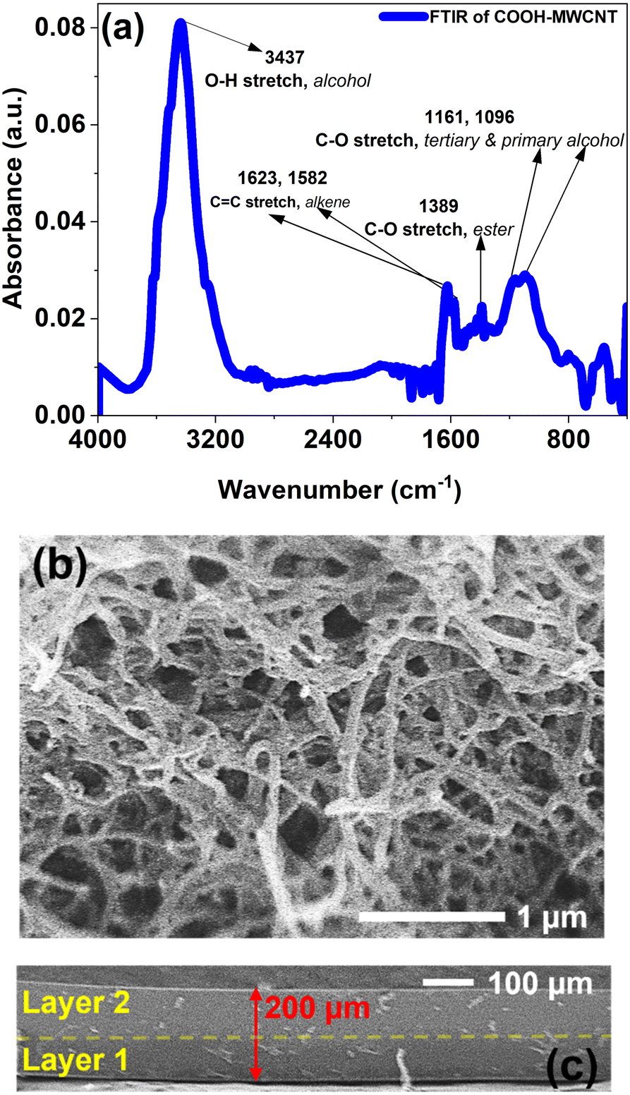
Fig. 5(a) shows the FTIR analysis of COOH–functionalized MWCNTs. The vibrations at 1161 cm−1 and 1096 cm−1 correspond to C–O stretches (tertiary and primary alcohol groups, respectively) of the –COOH functional group. The absorption peaks at 3437 cm−1 indicate the presence of hydroxyl groups (–OH) in the carboxylic group.47 The appearance of a peak at 1389 cm−1 corresponds to C–O stretching in ester groups, resulting from functional groups on the surface of the COOH–functionalized MWCNTs.47,48
 |
| | Fig. 5 (a) FTIR analysis of COOH–functionalized MWCNTs used in the fabrication of the nanocomposites, (b) FESEM image of the COOH–MWCNT bundles at a magnification of 25K×, and (c) cross-sectional FESEM analysis of the layered neat PDMS. | |
Fig. 5(b) and (c) are FESEM images of the COOH–MWCNT bundles and a cross-sectional view of the bi-layered neat PDMS sample. FESEM images of the MWCNT bundles (Fig. 5(b)) reveal the tubular and intertwined morphology of the nanotubes. The bi-layered neat PDMS without the MWCNT sandwich layer (Fig. 5(c)) is a control sample for the rest of the nanocomposite samples in this study. The bilayered neat PDMS structure confirms each layer thickness to be ∼100 μm and the total thickness of the sample as ∼200 μm. The thickness of the test structures with the MWCNT sandwich layer would accordingly vary based on the MWCNT layer thicknesses. The digital photos of the samples used in this work are shown in Fig. 6.
 |
| | Fig. 6 Photographic pictures of the test structures: (a) neat PDMS; (b)–(d) MWCNT sandwiched PDMS (1 wt%) – 3 samples fabricated under identical process conditions; (e)–(g) MWCNT sandwiched PDMS (3 wt%) – 3 samples fabricated under identical process conditions. | |
Measured EMI shielding effectiveness
Total EMI shielding effectiveness (SET) of the test structures represented through the |S21| values, viz., EMI SE = |S21|, where S21 is in dB, measured from VNA is shown in Fig. 7(a–f) and (g–l) for the X-band band and Ku-band, respectively.43 Each composite test structure shown in Fig. 6 was individually tested thrice to generate nine datasets for each sample type. The statistical reliability of the data is discussed in the ESI† in Section S2. The absorption coefficient (A), reflection coefficient (R) and transmission coefficient (T) are calculated from the S-parameters using the following equations.43,49
 |
| | Fig. 7 (a)–(f) and (g), and (h) show the shielding parameters in the X-band and Ku-band, respectively. Each plot corresponds to the total shielding effectiveness (SET) ((a) and (g)), shielding effectiveness due to reflection (SER) ((b) and (h)), and shielding effectiveness due to absorption (SEA) ((c) and (i)). The power coefficients governing the shielding effectiveness are also shown individually for (d) and (j) transmittance, (e) and (k) reflectance and (f) and (l) absorption. | |
Based on eqn (1)–(3), the shielding due to absorption (SEA) and shielding due to reflection (SER) are evaluated.43,49
| |
 | (5) |
Once an incident electromagnetic wave (EMW) enters the material, it can either be reflected, absorbed, or undergo multiple reflections within the shield. Hence, EMI shielding due to multiple reflections (SE
M) also needs to be considered and therefore, the total EMI SE (SE
T) can be expressed as,
| | |
SET = SER + SEA + SEM
| (6) |
However, the SE
M value can be ignored if SE
T ≥ 10 dB.
24 The measured
A,
R,
T, SE
T, SE
A and SE
R values of the various fabricated test structures in the X-band and Ku-band are respectively shown in
Fig. 6(a–c) and (g–i). As shown in
Fig. 7(c) and (i), in most of the test structures, the SE
A value is predominant.
Table 2 summarises the SE
T, SE
A and SE
R and the percentage of shielding contributed by the absorption process. From
Table 2, it can be inferred that, across all the nanocomposite test structures, 75–93% of the shielding is dominated by absorption and only 10–25% of the shielding is contributed by reflection. The variation of the obtained SE
T, SE
R and SE
A of the nanocomposites in the X-band (8.2–12.4 GHz) and Ku-band (12.4–18.0 GHz) frequency ranges is shown in
Fig. 7(a–c) and (g–i), respectively. For the 3 wt% MWCNT reinforced nanocomposites, the SE
T value is ∼23.3 dB (SE
R = 4.3 dB, SE
A = 19 dB) in the X-band and ∼23.2 dB (SE
R = 5 dB, SE
A = 18.2 dB) in the Ku-band, respectively. It is inferred that the SE
T of the nanocomposite reduces with an increase in frequency and is more efficient at a lower frequency domain. It can also be noted that the shielding due to absorption is significantly higher (75%–90% of shielding) than the SE
R in both frequency regions. The high MWCNT network density on a 2D plane at 3 wt% concentration facilitates a high-efficiency absorption process supported by multiple internal reflection processes to enhance the overall shielding efficiency of the incoming EM radiation.
Table 2 Percentage of shielding due to absorption (SEA) in the test structures
| Frequency (GHz) |
Sample name |
SET (dB) |
SER (dB) |
SEA (dB) |
SEA (%) |
| X-band (8.2–12.4 GHz) |
1 wt% MWCNT sandwiched PDMS |
15.3 |
3.7 |
11.6 |
75.8 |
| 3 wt% MWCNT sandwiched PDMS |
23.3 |
4.3 |
19.0 |
81.6 |
| Ku-band (12.4–18 GHz) |
1 wt% MWCNT sandwiched PDMS |
12.4 |
0.9 |
11.5 |
92.7 |
| 3 wt% MWCNT sandwiched PDMS |
23.2 |
5 |
18.2 |
78.5 |
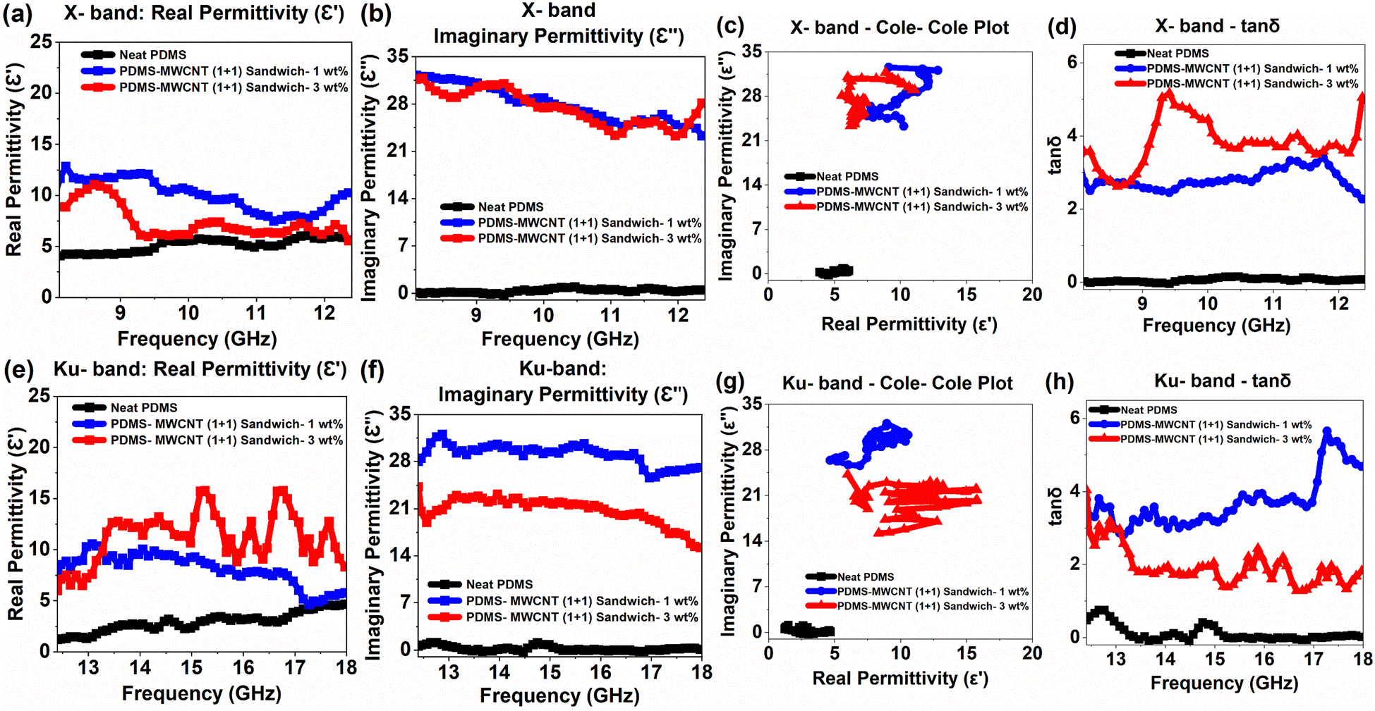
The variation of the real and imaginary parts of the complex permittivity (εr = ε′ − iε′′) of the nanocomposites in both the X-band and Ku-band is shown in Fig. 8(a, b) and (e, f), respectively. The corresponding Cole–Cole plots (ε′ vs. ε′′) and dielectric loss tangents plots (ε′′/ε′ vs. Frequency) are also shown in Fig. 8(c, g) and (d, h), respectively. ε′ corresponds to the storage ability of the electric energy density that occurs inside the material, and ε′′ corresponds to the dissipation of electrical energy.50–52 It is observed that both ε′ and ε′′ decrease with increasing frequency, attributed to the decrease of the interfacial polarization and heterogeneity between the PDMS matrix and carbon nanotube fillers.50,52,53 In the context of EMI shielding by polymer nanocomposite materials, a Cole–Cole plot provides insight into the dielectric relaxation behaviour of the material, revealing valuable information on the charge storage and dissipation characteristics within the nanocomposite.54 Fig. 8(c) and (g) are Cole–Cole plots of the nanocomposites corresponding to the X-band and Ku-band, respectively. Different relaxation arcs or semicircles in the plots correspond to interfacial polarization (Maxwell–Wagner–Sillars polarization),55 which is common in heterogeneous systems, such as the test structures considered in this study. The presence of multiple arcs indicates complex multi-phase dielectric relaxation, often due to the polymer matrix, fillers, and interfacial effects. Designing more interfaces in a test structure to increase interfacial polarization is an efficient method to attenuate high-frequency EM waves. Interface polarization typically occurs at a specific frequency.56 The prevailing view is that interface polarization influences the conductivity of the material system, which manifests as a peak in the high-frequency range. Additionally, the frequency at which interface polarization appears depends on the type of interface present. Notably, a larger change of ε′′ values (Δε′′ = ∼7) signifies stronger interface polarization behaviour.56 Furthermore, the relaxation behaviour is used as evidence of the strength of the interface polarization. In general, the relaxation process is represented by a Cole–Cole semicircle, with each semicircle corresponding to a Debye relaxation process.56 In the X-band, distinct Cole–Cole semicircles appear for nanocomposites with both 1 wt% and 3 wt% MWCNT concentrations (Fig. 8(c)), indicating a Debye relaxation process driven by interface polarization. However, in the Ku-band (Fig. 8(g)), the Cole–Cole semicircle is less noticeable due to the weaker intensity of interface polarization. The conversion of electromagnetic energy intrinsically relies on the dielectric loss tangent (tan![[thin space (1/6-em)]](https://www.rsc.org/images/entities/char_2009.gif) δ) values.57 tanδ plays a critical role in determining the SEA in EMI shielding. This relationship can be explained through standard physics expressions and the principles of wave attenuation within a lossy dielectric material. tanδ is given by57
δ) values.57 tanδ plays a critical role in determining the SEA in EMI shielding. This relationship can be explained through standard physics expressions and the principles of wave attenuation within a lossy dielectric material. tanδ is given by57
| |
 | (7) |
A higher tan
δ indicates that the material dissipates more of the electromagnetic energy into heat (
ε′′), which is beneficial for absorption. The attenuation of electromagnetic waves due to absorption is governed by the attenuation constant (responsible for energy dissipation),
α, given by
| |
 | (8) |
In non-magnetic test structures, the attenuation constant is fully governed by the dielectric constants. A higher tan
δ value indicates higher attenuation of EM waves through absorption. Peaks in the tan
δ plot suggest relaxation processes or resonant behaviours, which can be associated with the interfacial polarization mechanisms active at specific frequencies.
58 This is particularly useful for identifying at what frequency ranges the test structure performs best in terms of EMI absorption.
Fig. 8(d) and (h) are the tan
δ plots of the test structures in the X-band and Ku-band, respectively. In addition to these processes, energy transfer is also one of the key events that occur during the shielding provided by a heterogeneous polymer nanocomposite system with functional groups attached to the individual component species – PDMS and COOH–functionalized MWCNTs. As is well-known, PDMS is a synthetic elastomeric material predominantly comprising siloxane groups with a hydrophobic surface polarity. On the contrary, COOH–functionalized MWCNTs possess a hydrophilic surface polarity with active hydroxyl and carboxyl functional groups on their surface as discussed in the FTIR plot in
Fig. 5(a). Previous studies
59 have shown that charge density differences in these structures appear asymmetrical, suggesting the formation of dipoles. When exposed to an alternating electromagnetic field, these dipoles will detach, realign, and transform electromagnetic energy into thermal energy through a relaxation process.
60
 |
| | Fig. 8 Dielectric parameters of the test structures: (a) and (b) real and imaginary permittivity of the test structures in the X-band; (e) and (f) real and imaginary permittivity of the test structures in the Ku-band; neat PDMS (black curve), 1 wt% MWCNT sandwiched PDMS (blue curve), and 3 wt% MWCNT sandwiched PDMS (red curve); Cole–Cole plots of the test structures in the (c) X-band and (g) Ku-band; tanδ in the (d) X-band and (h) Ku-band. | |
EMI SE for multilayered structures simulated using CST
Based on experiments, it is understood that the 3 wt% MWCNT sandwiched test structures have EMI shielding capability up to ∼99.9% with a maximum SET of 23.3 dB. The thickness of this test structure was ∼0.7 mm with one layer of MWCNT sandwiched between two layers of PDMS. As discussed, the EMI SE in this structure is promoted significantly because of the absorption process, multiple internal reflections of the EM waves at the MWCNT and PDMS interfaces, interfacial polarization between MWCNT and PDMS and the corresponding energy transfer during relaxation in the layered structure. To understand the effect of an increased thickness of the test structure and an increase in the number of MWCNT layers on the SE, a CST simulation is conducted for the designs discussed in Table 1.
Fig. 9(a)–(f) show the CST simulation results for neat PDMS (X-band), PDMS–MWCNT (1 wt%) (X-band), PDMS–MWCNT (3 wt%) (X-band), neat PDMS (Ku-band), PDMS–MWCNT (1 wt%) (Ku-band), and PDMS–MWCNT (3 wt%) (Ku-band), respectively. As discussed in Table 1, each of the test structures is simulated for (1 + 1), (2 + 2), (3 + 3), (4 + 4) and (5 + 5) designs with the numbers corresponding to the numbers of PDMS and MWCNT layers in each design, respectively. The (1 + 1) simulation is a comparison to the experimentally measured values, and the experimentally measured data is also included in the individual graphs for comparison.
 |
| | Fig. 9 CST simulations of the EMI shielding effectiveness from (1 + 1) sandwich LBL to (5 + 5) sandwich LBL designs in the X-band and Ku-band for (a) and (d) neat PDMS, (b) and (e) MWCNT sandwiched PDMS (1 wt%) and (c) and (f) MWCNT sandwiched PDMS (3 wt%). | |
Assumptions made during CST simulations
The simulated samples were assumed to have a flat surface, while the experimental test structures possessed surface roughness due to the random arrangement of the MWCNT network on a 2D plane. In addition, the variation can also be partly connected with the automatic fitting of the input data (complex permittivity data, in this case) by CST Microwave Studio. Having this shortcoming, the simulated results still show significant improvement in the total shielding effectiveness (SET) values, with the (5 + 5) design consistently topping the performance across both samples in both frequency ranges. The (5 + 5) design of PDMS–MWCNT (3 wt%) with a thickness of 3.5 mm displayed a SET of −32.9 and −35.1 dB, respectively, in the X-band and Ku-band. The CST simulation done in this study is only a crude representation of the possibility of higher EM shielding when more CNT layers are present in the test structure. It is a conservative representation of the EMI shielding, while the actual experimental validation of the simulated structures could display only equivalent or higher shielding values.
This study represents a modest yet significant contribution to the field by demonstrating a shielding efficiency of 25–35 dB, achieved with MWCNT fillers at low concentrations (1–3 wt%) and thicknesses between 0.7 mm and 3.5 mm. Table 3 is a summary of the related PDMS–MWCNT-based nanocomposite structures evaluated for EMI SE. Similar SE has been reported by other groups with MWCNT at higher concentrations. A few studies which report similar SET values with lower CNT concentrations possess higher thicknesses. The multilayered MWCNT–reinforced PDMS nanocomposite introduced in this study represents a novel approach to the design of composites for electromagnetic interference (EMI) shielding. Our design features intrinsically layered structures unlike conventional multilayered composites, which are constructed by stacking bulk nanocomposites with varying filler types, contents, thicknesses, and shapes. In most prior works, fillers are dispersed within the bulk of the polymer matrix and then stacked over each other (extrinsic layers), typically achieved through layer-by-layer assembly processes. In contrast, our design inherently alternates PDMS and CNT layers without a dispersion step, creating a distinct 2D arrangement of the filler within each layer. This unique fabrication method not only ensures the presence of active filler material at a given concentration as layers throughout the cross-section of the multilayered composite but also significantly enhances the network density of the filler in each layer, thereby optimizing the EMI shielding performance. This approach, which emphasizes the intrinsic layering of the polymer and filler, offers a new perspective on composite design and is a key advancement in the field of EMI shielding. As the polymer layer thickness is reduced and the total number of layers of both the filler and polymer is increased, the proximity of the filler layers increases, thereby improving the network density of the filler on both the –XY plane and –Z plane. A theoretical calculation, discussed in the ESI† (Section S3), revealed that the number of CNTs per unit volume in the first 1 μm depth of the composite on a 2D distribution is 25× more than a 3D distribution for the same amount of CNTs. This significant improvement in the network density is the key reason for the enhanced EMI shielding performance of this design at low concentrations of MWCNT at lower thickness values, as well.
Table 3 Literature review table collating the shielding effectiveness offered by state-of-the-art MWCNT reinforced PDMS nanocomposites
| S. no. |
Polymer |
Thickness (mm) |
Filler concentration |
SET (dB) |
Frequency (GHz) |
Conductivity (σDC) |
SER (dB) |
SEA (dB) |
Ref. |
| 1. |
PDMS–MWCNT (spin-coated) |
0.15 |
0.5 wt% |
2.0 |
Ku-band |
— |
— |
— |
24 |
| 1.5 wt% |
7.5 |
— |
— |
|
| 3 wt% |
13.5 |
7.2 × 10⁻¹ S cm−1 |
— |
— |
| PDMS–MWCNT (compression moulded) |
0.18 |
7.0 |
4.1 × 10⁻¹ S cm−1 |
— |
— |
| PDMS–MWCNT multilayer (spin-coated) |
0.90 |
(3 + 1.5 + 0.5 + 0.5 + 1.5 + 3) wt% |
26.0 |
— |
— |
|
| 2. |
PDMS–MWCNT (three-roll milled + compression moulded) |
2.0 |
0.1 vol% |
10.0 |
X-band |
— |
— |
— |
23 |
| 0.3 vol% |
12.0 |
— |
— |
— |
| 0.6 vol% |
15.0 |
1.5 S m−1 |
— |
— |
| 1.7 vol% |
38.0 |
— |
— |
— |
| 2.8 vol% |
44.0 |
— |
— |
— |
| 3. |
PDMS–MWCNT-expandable polymeric microspheres (EPMs) foam |
2.0 |
1.78 wt% |
17.8 |
X-band |
7.93 S m−1 |
— |
— |
26 |
| 6.78 wt% |
44.5 |
44.23 S m−1 |
3.79 |
40.7 |
| 4. |
CNT-coated partially cured PDMS microspheres embedded in PDMS matrix |
1.0 |
0.8 vol% |
10.5 |
X-band |
7.7 S m−1 |
1 |
9.5 |
15 |
| 1.3 vol% |
17.0 |
13.9 S m−1 |
1.8 |
15.2 |
| 1.8 vol% |
21.5 |
24.2 S m−1 |
1.8 |
19.7 |
| 2.2 vol% |
27.0 |
64.6 S m−1 |
2.5 |
24.5 |
| 5. |
PDMS–MWCNT films (two roll milled + compression molded) |
3.0 |
1 wt% |
9.0 |
X-band |
0.19 S cm−1 |
— |
— |
25 |
| 2 wt% |
17.0 |
0.35 S cm−1 |
— |
— |
| 4 wt% |
34.5 |
0.68 S cm−1 |
8.5 |
26 |
| 5 wt% |
44.0 |
0.80 S cm−1 |
— |
— |
| 6 wt% |
49.0 |
0.85 S cm−1 |
13.5 |
35.5 |
| 6. |
CNT sponge–PDMS (vacuum impregnation method) |
2.0 |
1 wt% |
46.3 |
X-band |
— |
0.5 |
45.8 |
40 |
| 7. |
CNT sponge–PDMS (vacuum impregnation method) |
1.0 |
1 wt% |
34.6 |
X-band |
53 S m−1 |
1.46 |
33.10 |
27 |
| CNT–PDMS bulk composite |
3 wt% |
3.8 |
2.78 × 10⁻³ S m−1 |
0.75 |
3 |
| 5 wt% |
5.5 |
4.68 × 10⁻³ S m−1 |
0.5 |
5 |
| 10 wt% |
12.0 |
5.47 × 10⁻¹ S m−1 |
2 |
10 |
| 15 wt% |
21.5 |
1.56 S m−1 |
3 |
18.5 |
| 8. |
PDMS–MWCNT, sandwich structure-(1 + 1) LBL (experimentally measured) |
0.4 |
1 wt% |
15.3 |
X-band |
— |
3.7 |
11.6 |
This work |
| 12.4 |
Ku-band |
— |
0.9 |
11.5 |
| 0.7 |
3 wt% |
23.3 |
X-band |
— |
4.3 |
19.0 |
| 23.2 |
Ku-band |
— |
5 |
18.2 |
| 9. |
PDMS–MWCNT, sandwich structure-multilayers: (1 + 1) to (5 + 5) LBL (CST simulations) |
0.4 |
1 wt% |
8.6 |
X-band |
— |
— |
— |
| 0.8 |
12.6 |
— |
— |
— |
| 1.2 |
15.3 |
— |
— |
— |
| 1.6 |
17.9 |
— |
— |
— |
| 2.0 |
20.8 |
— |
— |
— |
| 0.4 |
10.3 |
Ku-band |
— |
— |
— |
| 0.8 |
14.9 |
— |
— |
— |
| 1.2 |
18.8 |
— |
— |
— |
| 1.6 |
23.1 |
— |
— |
— |
| 2.0 |
27.7 |
— |
— |
— |
| 0.7 |
3 wt% |
11.7 |
X-band |
— |
— |
— |
| 1.4 |
16.7 |
— |
— |
— |
| 2.8 |
21.8 |
— |
— |
— |
| 3.5 |
27.4 |
— |
— |
— |
| 4.2 |
32.9 |
— |
— |
— |
| 0.7 |
11.3 |
Ku-band |
— |
— |
— |
| 1.4 |
16.7 |
— |
— |
— |
| 2.8 |
22.8 |
— |
— |
— |
| 3.5 |
29.1 |
— |
— |
— |
| |
4.2 |
35.1 |
— |
— |
— |
Mechanism of shielding
The design discussed in this study involves alternating layers of MWCNT and PDMS in the composite, unlike the conventional designs wherein the filler is dispersed in the bulk of the polymer matrix. Due to this, the proximity of interfaces and the significance of interfacial polarization at each interface increase. In this stacked design, there are three specific interfaces that actively and parallelly perform the shielding process. As the CNT is distributed on a 2D plane, even when the network density is high, there will be voids between the CNT network, leading to a PDMS–PDMS interface (polymer–polymer interface). While polymer–polymer interfaces do not directly participate in the electromagnetic attenuation mechanisms, they are vital for the structural and functional performance of polymer-based EMI shielding composites. The second interface is the interface between the CNTs. As the network density is significantly enhanced on the 2D plane, the numbers of interfaces between CNTs also increase more than the number in a 3D distribution. This facilitates the multiple reflection and enhanced absorption processes of the incoming EM wave. The third interface is the CNT–PDMS interface (filler–polymer interface). The discussed phenomena, such as the interfacial polarization and energy transfer mainly occur at this interface. In addition, due to the layered arrangement of the test structures, there is a significant impedance mismatch between CNT and PDMS between the consecutive layers of the test structure. The random 2D arrangement of CNTs and the varying CNT layer thickness based on the network density promote the impedance mismatch within the same layer as well as between consecutive layers. Because of the multiple interfaces resulting in many mismatched impedances across every interface, the absorption of the incoming EM wave is significantly boosted. Based on this, a schematic depicting the EMI shielding process involving the key events occurring at different interfaces is shown in Fig. 10.
 |
| | Fig. 10 Mechanism of shielding depicting the key events contributing to EMI shielding occurring at the different interfaces. | |
Green shielding
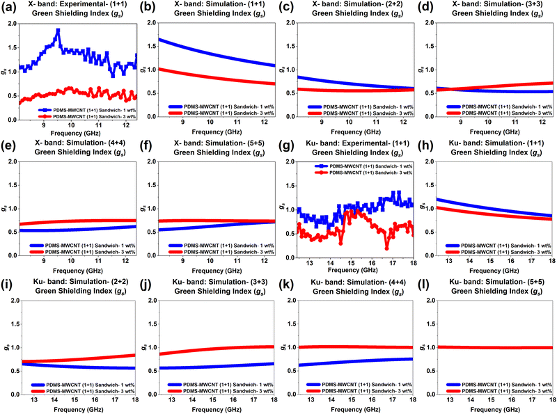
EM absorbing materials with good impedance matching could remove the incident EM waves and at the same time cause no secondary reflections, which are the most desirable EMI shielding materials.61 However, there has not been a mathematical standard for the definition of absorption shielding materials until Cao et al.62 proposed the green index (gs) as a criterion for low-reflection (absorptive) EMI shielding materials. “Green” refers to EMI shielding materials that are minimally harmful or harmless to both the internal environment—protecting bodies or workspaces from electromagnetic radiation—and the external environment, meaning that they pose no threat to other living beings or ecosystems.63 In 2022, Hwang et al.64 introduced an essential criterion for absorption predominant EMI shielding materials, stating that the electromagnetic wave (EMW) loss from surface reflection (SER) should be below 3.01 dB. However, most EMW-absorbing materials have been developed without considering the gs index and SER standard, which can significantly overestimate their absorption and reflection capabilities. Achieving both high EM attenuation and eco-friendliness in green EMI shielding materials remains a considerable challenge. The gs value is calculated using the following equation:65| |
 | (9) |
A flexible, green (gs ≥ 1), absorption-based (SER < 3.01) material is considered an ideal absorptive EMI shielding material. To obtain a high SE and gs simultaneously, green EMI shielding materials should have both favourable impedance matching and excellent EM attenuation capability.66 The manipulation of the microstructure is an important way to achieve a balance between the two. In this study, the design of the test structures has manipulated the microstructure to increase the interface density, promoting absorption (SEA). In addition, the high CNT network density promotes multiple internal reflections and scattering, leading to attenuation and dissipation of EMW, reducing the overall secondary reflection (SER). Based on eqn (9), the gs of all the experimental and simulated composite test structures considered in this study are calculated and are depicted in Fig. 11(a)–(l). Generally, gs is discussed when EMI SE is larger than the commercial standard of 20 dB.67–69 When gs > 1, the EMI shield absorbs most of the incident wave that enters the material, becoming eco-friendly. Furthermore, when both criteria, i.e. gs > 1 and SE closer or larger than 20 dB, the material can be considered a highly efficient green EMI shield.69 It is inferred that both in the X-band and Ku-band, the PDMS–MWCNT (1 wt%) with SER < 3.01 dB has turned out to be the candidate with gs > 1 topping the chart as the most suitable green shielding material both in the experimental and simulated designs with an SET ranging between 15–20 dB in the X-band and 15–28 dB in the Ku band in experimentally measured and simulated designs. MWCNT–reinforced PDMS layered nanocomposites with 1 wt% filler content possess the optimal internal structure and conductivity that balance both polarization and impedance mismatch-driven absorption, adequate scattering across consecutive layers to dissipate the EM waves, and conduction-driven minimal reflection losses, enabling simultaneous efficient EM absorption and shielding.
 |
| | Fig. 11 Green shielding index of the nanocomposites from experiments and simulations. (a)–(f): Experimental and simulation results for X-band and (g)–(l): experimental and simulation results for Ku-band. | |
Conclusions
This study presents a multilayered MWCNT–reinforced PDMS composite with an innovative layer arrangement, achieving 25× higher CNT network density than the 3D dispersion. With 3 wt% MWCNT, the composite achieves ∼25 dB EMI shielding (99.9%) in the X- and Ku-bands at 0.7 mm thickness, outperforming prior designs. Simulations suggest ∼35 dB shielding (99.99%) at ∼3.5 mm thickness. The shielding is ∼80% absorption-driven, highlighting its potential for efficient EMI shielding.
Using Cole–Cole and dielectric loss tangent analysis, this study reveals CNT–reinforced PDMS multilayered nanocomposites for EMI shielding effectiveness, mechanisms, and power coefficients. Interfacial polarization and shielding mechanisms are discussed, emphasizing interface roles in this novel design. The PDMS–MWCNT (1 wt%) composite emerges as the ideal green shielding material, achieving SER < 3.01 dB, gs ≥ 1, and ∼15 dB SET (>90% shielding) in both the X- and Ku-bands.
This structure achieves high SET values with absorption-driven shielding at low MWCNT concentrations (1–3 wt%) and thicknesses (0.4–3.5 mm). The facile fabrication process allows quick optimization of PDMS and CNT layer thicknesses and orientations. The self-assembled MWCNT network enhances interface density, boosting absorption via impedance differences within and between consecutive layers, interfacial polarization and energy transfer. However, limitations in this design include non-isotropic properties in the –XY and –Z planes and scalability challenges in maintaining uniform MWCNT arrangements, requiring larger sampling plans to assess shielding variability comprehensively.
Future work will focus on stacking test structures with varying MWCNT concentrations to achieve optimal SET with minimal thickness and filler content. This approach uniquely combines intrinsic (PDMS–CNT alternation) and extrinsic (stacked composites) layers to enhance shielding mechanisms. Simulations on geometry and charge distribution, along with integrating electrically and magnetically active fillers, offer a transformative potential to significantly boost shielding performance, making this composite design a robust solution for advanced EMI shielding applications.
Author contributions
Pavithra Ananthasubramanian: conceptualization, methodology, validation, formal analysis, investigation, data curation, visualization, writing – original draft, writing – review and editing; Pritom J Bora: conceptualization, methodology, formal analysis, investigation, writing – review and editing, supervision; Chandana Gadadasu: methodology, validation, investigation, data curation, Praveen C Ramamurthy: project administration and Nagarajan Raghavan: conceptualisation, writing – review and editing, supervision, project administration, funding acquisition.
Data availability
The data that support the findings of this study are available in the main text, ESI,† as well as, from the corresponding authors upon request.
Conflicts of interest
There are no conflicts to declare.
Acknowledgements
The first and last authors are grateful for the research surplus grant “RGSUR08” towards the funding of this project. They also thank Prof. Yang Hui Ying at the Singapore University of Technology and Design (SUTD) for sharing their chemical laboratory facility for wet chemical experiments in this study. They thank the cleanroom facility in SUTD, which was used to fabricate the test structures. The first author acknowledges SUTD and the Ministry of Education, Singapore (MOE) for the Research Student Scholarship (RSS) and SUTD PhD Fellowship for her doctoral studies from 2021–2025. All the authors are thankful to the Interdisciplinary Centre for Energy Research (ICER), Indian Institute of Science, Bangalore, 560012, India, for access to the Vector Network Analyser.
References
- A. K. Mallick, Handbook of Green Engineering Technologies for Sustainable Smart Cities, 2021, pp. 57–82 Search PubMed.
- I. F. Akyildiz, A. Kak and S. Nie, IEEE Access, 2020, 8, 133995 Search PubMed.
- V. Mordachev, Doklady BGUIR, 2020, 18, 96–112 CrossRef.
- M. Kaur, S. Kakar and D. Mandal, Electromagnetic interference, in 2011 3rd international conference on electronics computer technology, IEEE, 2011, vol. 4, pp. 1–5.
- M. Solkin, Transp. Res. Procedia, 2021, 59, 310–318 Search PubMed.
- F. Ozdemir and A. Kargi, Electromagn. Waves, 2011, 22, 475–491 Search PubMed.
- D. Chung, Mater. Chem. Phys., 2020, 255, 123587 CrossRef CAS.
- S. Geetha, K. Satheesh Kumar, C. R. Rao, M. Vijayan and D. Trivedi, J. Appl. Polym. Sci., 2009, 112, 2073–2086 CrossRef CAS.
- D. Wanasinghe and F. Aslani, Composites, Part B, 2019, 176, 107207 Search PubMed.
- J. Kruželák, A. Kvasničáková, K. Hložeková and I. Hudec, Nanoscale Adv., 2021, 3, 123–172 RSC.
- M. Zahid, R. Anum, S. Siddique, H. F. Shakir and Z. Rehan, J. Thermoplast. Compos. Mater., 2023, 36, 1717–1761 Search PubMed.
- Z. He, H. Xie, H. Wu, J. Chen, S. Ma, X. Duan, A. Chen and Z. Kong, ACS Omega, 2021, 6, 22468–22477 CrossRef CAS PubMed.
- P. J. Bora, A. G. Anil, K. J. Vinoy and P. C. Ramamurthy, Adv. Mater. Interfaces, 2019, 6, 1901353 CrossRef CAS.
- D. Sharma and S. Bose, Mater. Adv., 2021, 2, 5580–5592 Search PubMed.
- R.-Y. Ma, S.-Q. Yi, J. Li, J.-L. Zhang, W.-J. Sun, L.-C. Jia, D.-X. Yan and Z.-M. Li, Compos. Sci. Technol., 2023, 232, 109874 CrossRef CAS.
- P. Song, B. Liu, C. Liang, K. Ruan, H. Qiu, Z. Ma, Y. Guo and J. Gu, Nano-Micro Lett., 2021, 13, 1–17 CrossRef PubMed.
- L. Xu, S. Wan, Y. Heng, S. Wang, J. Yang, Y. Dong, Y. Fu and Q. Ni, Compos. Sci. Technol., 2023, 231, 109797 CrossRef CAS.
- V.-T. Nguyen, B. K. Min, Y. Yi, S. J. Kim and C.-G. Choi, Chem. Eng. J., 2020, 393, 124608 Search PubMed.
- K. Liu, C. Yang, L. Song, Y. Wang, Q. Wei, Q. Deng and N. Hu, Compos. Sci. Technol., 2022, 218, 109148 Search PubMed.
- A. Ghasemi, H. Amiri, H. Zare, M. Masroor, A. Hasanzadeh, A. Beyzavi, A. R. Aref, M. Karimi and M. R. Hamblin, Microfluid. Nanofluid., 2017, 21, 1–19 CrossRef PubMed.
- J. H. Kim, J.-Y. Hwang, H. R. Hwang, H. S. Kim, J. H. Lee, J.-W. Seo, U. S. Shin and S.-H. Lee, Sci. Rep., 2018, 8, 1375 Search PubMed.
- M. H. Al-Saleh and U. Sundararaj, Carbon, 2009, 47, 1738–1746 Search PubMed.
- P. Theilmann, D.-J. Yun, P. Asbeck and S.-H. Park, Org. Electron., 2013, 14, 1531–1537 Search PubMed.
- H. Nallabothula, Y. Bhattacharjee, L. Samantara and S. Bose, ACS Omega, 2019, 4, 1781–1790 Search PubMed.
- S. Panda and B. Acharya, J. Mater. Sci.: Mater. Electron., 2021, 32, 16215–16229 CrossRef CAS.
- Z. Xie, Y. Cai, Z. Wei, Y. Zhan, Y. Meng, Y. Li, Y. Li, Q. Xie and H. Xia, Compos. Commun., 2022, 35, 101323 CrossRef.
- L. Liu, J. Liu, R. Wang, X. Li, H. Guo, J. Tang and J. Liu, J. Electron. Mater., 2023, 52, 429–436 CrossRef CAS.
- H. Zhang, G. Zhang, M. Tang, L. Zhou, J. Li, X. Fan, X. Shi and J. Qin, Chem. Eng. J., 2018, 353, 381–393 CrossRef CAS.
- S. Chandrasekaran, G. Faiella, L. A. Prado, F. Tölle, R. Mülhaupt and K. Schulte, Composites, Part A, 2013, 49, 51–57 CrossRef CAS.
- M. Jung, Y.-s Lee, S.-G. Hong and J. Moon, Cem. Concr. Res., 2020, 131, 106017 Search PubMed.
- W.-C. Yu, J.-Z. Xu, Z.-G. Wang, Y.-F. Huang, H.-M. Yin, L. Xu, Y.-W. Chen, D.-X. Yan and Z.-M. Li, Composites, Part A, 2018, 110, 237–245 Search PubMed.
- D. Feng, D. Xu, Q. Wang and P. Liu, J. Mater. Chem. C, 2019, 7, 7938–7946 RSC.
- P. Ananthasubramanian, R. Sahay and N. Raghavan, Sci. Rep., 2024, 14, 4487 CrossRef CAS PubMed.
- P. Ananthasubramanian, R. Sahay and N. Raghavan, Examining Stretch Marks in Soft Composites Using Field Emission Scanning Electron Microscope Assisted in-situ Nanoindentation Analysis, in 2024 IEEE 14th International Conference Nanomaterials: Applications & Properties (NAP), IEEE, 2024, pp. 1–7.
- P. Ananthasubramanian, R. Sahay and N. Raghavan, Understanding the Cohesive and Adhesive Failures in Novel Multilayered SWCNT-Reinforced PDMS Composites using Nano Scratch Technique, in 2024 IEEE 14th International Conference Nanomaterials: Applications & Properties (NAP), IEEE, pp. 1–8.
- C.-F. Cao, P.-H. Wang, J.-W. Zhang, K.-Y. Guo, Y. Li, Q.-Q. Xia, G.-D. Zhang, L. Zhao, H. Chen and L. Wang, Chem. Eng. J., 2020, 393, 124724 CrossRef CAS.
- J. Li, X. Lan, S. Lei, J. Ou-Yang, X. Yang and B. Zhu, Carbon, 2019, 145, 112–118 Search PubMed.
- A. S. Miroshnichenko, V. Neplokh, I. S. Mukhin and R. M. Islamova, Materials, 2022, 15, 8731 Search PubMed.
- M. Zhang, L. Shao, T. Zhang, Y. Yang, X. Li and J. Ma, Polym. Compos., 2024, 45, 4002–4013 Search PubMed.
- D. Lu, Z. Mo, B. Liang, L. Yang, Z. He, H. Zhu, Z. Tang and X. Gui, Carbon, 2018, 133, 457–463 CrossRef CAS.
- S. Pande, B. Singh, R. Mathur, T. Dhami, P. Saini and S. Dhawan, Nanoscale Res. Lett., 2009, 4, 327–334 Search PubMed.
- V. Sachdev, S. Sharma, M. Tomar, V. Gupta and R. Tandon, RSC Adv., 2016, 6, 45049–45058 RSC.
- Y. Yang, M. C. Gupta, K. L. Dudley and R. W. Lawrence, Nano Lett., 2005, 5, 2131–2134 CrossRef CAS PubMed.
- D. Micheli, C. Apollo, R. Pastore, R. B. Morles, M. Marchetti and G. Gradoni, Adv. Nanocompos. Synth.:Synth., Charact. Ind. Appl., 2011, 360–384 Search PubMed.
- P. Liu, L. Li, L. Wang, T. Huang, Q. L. Zhao, K. L. Zhang, X. M. Bian and Z. L. Hou, Phys. Status Solidi A, 2017, 214, 1700589 Search PubMed.
- P. J. Bora, A. G. Anil, P. C. Ramamurthy and D. Q. Tan, Mater. Adv., 2020, 1, 177–183 RSC.
- A. Hamed Mashhadzadeh, A. Fereidoon and M. Ghorbanzadeh Ahangari, Appl. Surf. Sci., 2017, 420, 167–179 CrossRef CAS.
- S. Yellampalli, Carbon Nanotubes: Polymer Nanocomposites, BoD–Books on Demand, 2011 Search PubMed.
- Y.-J. Tan, J. Li, J.-H. Cai, X.-H. Tang, J.-H. Liu, Z.-Q. Hu and M. Wang, Composites, Part B, 2019, 177, 107378 Search PubMed.
- J. W. Gooch and J. K. Daher, Electromagnetic shielding and corrosion protection for aerospace vehicles, Springer, 2007 Search PubMed.
- Y. Zhang, Z. Wang, B. Zhang, C. Zhou, G.-L. Zhao, J. Jiang and S. Guo, J. Mater. Chem. C, 2015, 3, 9684–9694 RSC.
- P. J. Bora, G. Lakhani, P. C. Ramamurthy and G. Madras, RSC Adv., 2016, 6, 79058–79065 RSC.
- X. C. Tong, Advanced materials and design for electromagnetic interference shielding, CRC Press, 2016 Search PubMed.
- Z. Jan and J. Maciej, Electromagn. Waves, 2011, 425–448 Search PubMed.
- M. Samet, A. Kallel and A. Serghei, J. Compos. Mater., 2022, 56, 3197–3217 CrossRef CAS.
- H. Lv, Y. Guo, G. Wu, G. Ji, Y. Zhao and Z. J. Xu, ACS Appl. Mater. Interfaces, 2017, 9, 5660–5668 CrossRef CAS PubMed.
- P. J. Bora, G. Chandana, B. Mahanta, J. Doh, P. C. Ramamurthy and N. Raghavan, Compos. Commun., 2023, 39, 101568 CrossRef.
- L. Y. Seng, F. Wee, H. Rahim, F. Malek, K. You, Z. Liyana, M. Jamlos and A. Ezanuddin, Appl. Phys. A:Mater. Sci. Process., 2018, 124, 1–7 CrossRef CAS.
- N. Ghaderi and M. Peressi, J. Phys. Chem. C, 2010, 114, 21625–21630 CrossRef CAS.
- M. Cao, X. Wang, W. Cao, X. Fang, B. Wen and J. Yuan, Small, 2018, 14, 1800987 Search PubMed.
- B. Ray, S. Parmar, K. Date and S. Datar, J. Appl. Polym. Sci., 2021, 138, 50255 Search PubMed.
- D.-Q. Zhang, T.-T. Liu, J.-C. Shu, S. Liang, X.-X. Wang, J.-Y. Cheng, H. Wang and M.-S. Cao, ACS Appl. Mater. Interfaces, 2019, 11, 26807–26816 CrossRef CAS PubMed.
- S. Zhao, L. Yan, X. Tian, Y. Liu, C. Chen, Y. Li, J. Zhang, Y. Song and Y. Qin, Nano Res., 2018, 11, 530–541 CrossRef CAS.
- U. Hwang, J. Kim, M. Seol, B. Lee, I.-K. Park, J. Suhr and J.-D. Nam, ACS Omega, 2022, 7, 4135–4139 CrossRef CAS PubMed.
- S. Li, Y. Jiang, L. Zhu, H. Dai, C. Tang, L. Liu, C. Gu and Z. Li, ACS Appl. Electron. Mater., 2022, 4, 5632–5640 CrossRef CAS.
- X.-X. Wang, Q. Zheng, Y.-J. Zheng and M.-S. Cao, Carbon, 2023, 206, 124–141 CrossRef CAS.
- R. B. Marks, J. A. Jargon and J. R. Juroshek, Calibration comparison method for vector network analyzers, in 48th ARFTG conference digest, IEEE., 1996, vol. 30, pp. 38–45.
- M. Mohamadi, E. Kowsari, V. Haddadi-Asl and M. Yousefzadeh, Composites, Part B, 2019, 162, 569–579 CrossRef CAS.
- A. Uddin, R. Khatoon, D. Estevez, M. Salem, A. Ali, S. Attique, J. Lu and F. Qin, Mater. Today Commun., 2022, 31, 103858 CrossRef CAS.
|
| This journal is © The Royal Society of Chemistry 2025 |
Click here to see how this site uses Cookies. View our privacy policy here. 
 Open Access Article
 This Open Access Article is licensed under a
  a,
Pritom J. Bora
a,
Pritom J. Bora