DOI:
10.1039/D5MA00207A
(Paper)
Mater. Adv., 2025,
6, 3605-3611
Low-temperature APPJ printing of Kesterite on flexible substrates for heterojunction solar cells†
Received
7th March 2025
, Accepted 13th April 2025
First published on 14th April 2025
Abstract
Kesterite Cu2ZnSnS4 (CZTS), composed of earth-abundant, non-toxic elements, is considered a promising chalcogenide photoabsorber. One of the major roadblocks in its large-scale implementation is limited scalability for roll-to-roll fabrication at low temparatures. Herein, we reported an ambient-air deposition method for CZTS films onto rigid as well as flexible surfaces at a low temperature (∼170 °C) and tested their applicability in heterojunction solar cells. In this process, the precursor solution was directly coated onto conductive substrates using an atmospheric pressure plasma jet (APPJ). The rich chemistry of APPJ was used to engineer the surface energy of the substrates, while the charged particles, neutral metastable species, and radicals were used to activate reactions that were thermodynamically unfavorable under ambient conditions. Here, we carefully controlled a high temperature in the plasma while maintaining a low temperature at the substrate. This open-air processing overcame the complex and high-temperature (∼500 °C) requirements for controlled sulfurization or selenisation. By employing an environmentally benign molecular precursor made with a green solvent, our method aligned well with the increasing demand for industry-relevant, eco-friendly manufacturing processes. The plasma-printed CZTS showed p-type characteristics and a band gap in the visible region. As a proof of concept, we measured the power conversion efficiencies (PCEs) of functional CZTS/CdS heterojunction solar cells on both rigid ITO substrates (~3.1%) and flexible ITO substrates (~1.1%). The measured PCEs set new benchmarks for low-temperature-processed CZTS devices. Through favourable engineering of interfacial layers and the integration of passivation layers, higher efficiency and stability could be achieved.
1. Introduction
Metal chalcogenides are recognized as promising candidates for the absorber material in the advancement of cost-effective thin-film solar cells.1,2 Cu2ZnSnS4 (CZTS) has emerged as a green replacement option for CdTe and CIGS in thin-film solar cells, owing to its high absorption coefficient (104 cm−1), optimum band gap (Eg) (1.0–1.5 eV), and earth-abundant, environmentally friendly constituents.3–5 Recently, considerable advancements have been made in this material's PCE, attaining up to 14.9%.6–12 Several deposition techniques have been employed to prepare CZTS films, such as thermal, co-evaporation,13 electrodeposition,14 sputtering,15 and solution-based techniques.16 In particular, low-temperature solution processing of CZTS is being pursued to facilitate the scalable and low-cost fabrication of thin-film solar cells on both rigid and flexible substrates.11,17–19 However, the toxicity of solvents used and the high-temperature annealing processes required for fabricating high quality absorbers are major hindrances to making it compatible with large-scale, low-cost manufacturing.2,20,21 Several non-toxic solvent-based precursor solutions or inks for making CZTS films have been explored using dimethyl sulfoxide (DMSO), ethanol, N,N-dimethyl formamide (DMF), 2-methoxyethanol, and 1,3-dimethyl-2-imidazolidinone (DMI).21–27 However, a high-temperature annealing process is generally required to reduce the impurity phases (CuS, ZnS, and SnS) and achieve better crystalline quality of the CZTS film on both rigid and flexible substrates.2,20,21,28–30 For instance, a sulfurization temperature of 550 °C on a rigid substrate was advantageous for the crystal development of CZTS, and its primary effects on the electrical, photovoltaic, and morphological characteristics were analyzed by Payno et al.28 A sol–gel process-based CZTS formed on molybdenum (Mo) foil at 500 °C resulted in a device with a PCE of 2.25%, and electrochemically deposited CZTS gave a PCE of 3.82%.29,30 CZTS particles were printed on Mo-coated aluminum foil/flexible polyimide substrates to make devices with a PCE of 1–1.94%.30,31 A polyimide (PI) substrate-based device was reported by Romero et al.,32 where the fabrication of kesterite (CZTSe) required a high temperature (∼490 °C), similar to the other examples mentioned above.
It is worth noting that most of these reports on flexible devices still require an annealing process at high temperatures, and thus use Mo-coated Al foil,30 Ti foil,33 stain less steel foil, flexible glass (FG, corning willow glass),34 or polyimide (PI) substrates.32 Such rigorous processing conditions could hinder their future advancement, predominantly in devices with flexible formats involving polymer substrates. A few of the reported low-temperature process-based devices were inferior in terms of efficiency compared to those based on high-temperature processing.32,35–43 The efficiency reduction primarily stems from charge recombination occurring at flawed interfaces and the presence of structural or chemical defects within the CZTS film. For example, the low-temperature processed glass/ITO/CZTS/CdS/Al devices showed a PCE of 1.34% to 1.85%.40,44 Further, Saha et al.45 introduced an additional layer of Ag-doped CZTS at the interface of CZTS/CdS to improve the depletion region architecture and carrier collection. Farinella et al.44 reported a good-quality CZTS thin film made via electrochemical deposition on flexible PET/ITO substrates at room temperature, but no device was fabricated. Recently, Dhanasekar et al. fabricated a dip-coated CZTS absorber on a flexible (PET/ITO) substrate with low-temperature annealing in an argon (Ar) atmosphere, resulting in a device exhibiting a PCE of up to 0.74%.46,47 Further exploration in this direction is highly desired to achieve more efficient devices for flexible electronics applications.
Printed and flexible electronics have expanded into many domains, including photovoltaics. The most common printing techniques for solution-processed thin films are inkjet printing48 and aerosol printing.49 However, both of these approaches require a sintering step or post-thermal annealing to form a thin film. Atmospheric pressure plasma jet (APPJ) is a printing technology that uses atmospheric pressure cold plasma to deposit materials onto a substrate. It can be used to print high-quality materials at low temperatures and in open atmospheres using precursor solutions. The quality and integrity of the film can be improved with this plasma-based process due to the increase in surface tension and wetting properties of the precursor solution. The rich physical and chemical properties of APPJ,50 suitable for applications in material processing, healthcare, nanotechnology, and medicine, are widely being explored.51 APPJ can be utilized for printing nano-colloid inks while simultaneously tuning the surface chemistry and electronic properties of the material being printed. For example, it can reduce highly acidic graphene oxide to graphene in situ without the need for any external post-processing.52 High-capacity graphite anodes based on APPJ have been studied for the environmentally friendly reuse of lithium-ion batteries.53 Inspired by these observations, we sought to explore the APPJ technique to print the nanocrystalline CZTS solar absorber at low temperatures under open atmosphere. An environmentally friendly molecular precursor solution was used for the APPJ printing of nanocrystalline CZTS, and simple heterojunction solar cells were fabricated on both rigid and flexible substrates to demonstrate the device application. The results were compared with those obtained using the dip-coated CZTS film annealed under an Ar atmosphere, as well as with other relevant reports from the literature.
2. Experimental section
2.1. Materials
Copper chloride, zinc acetate dihydrate, cadmium chloride monohydrate, propylamine, butylamine, thioacetamide (TAA), and thiourea were purchased from Sisco Research Laboratories Pvt. Ltd. (SRL). Tin chloride dihydrate and 2-methoxyethanol were obtained from Alfa Aesar. Gold was purchased from GRT Gold Jewellery, Chennai, India. Indium-doped tin oxide (ITO) and polyethylene terephthalate (PET)/ITO were procured from Global Nanotech, India. Ethanol, isopropyl alcohol (IPA), and deionized (DI) water were used for cleaning the substrates. The chemicals were used without any additional purification steps.
2.2. Preparation of precursor solution of CZTS
10 mL of 2-methoxyethanol was used to gradually dissolve 1.88 g of copper chloride, 2.19 g of zinc acetate dihydrate, 1.8 g of tin chloride dihydrate, and 4.8 g of thioacetamide at room temperature. The composition ratio of Cu, Zn, Sn, and S was kept within a suitable range: Zn/Sn = 1.25, S/(Cu + Zn + Sn) = 1.88, and Cu/(Zn + Sn) = 0.8.54,55 The concentration of the precursor solution was varied according to the requirements for the coating, and a 50% dilution with additional solvent was optimal for APPJ printing.
2.3. APPJ printing and dip coating of CZTS film
APPJ was generated using a quartz nozzle connected to a 15 kV nanosecond pulse generator. Helium gas was used as the carrier gas. A specially designed Teflon nebulizer was used to create an aerosol of the precursor solution, which was generated using the He gas flow. This aerosol was then fed into the plasma and deposited onto the substrate via the plasma plume/jet. The operational condition parameters optimized for the APPJ printing of CZTS film were as follows: the diameter of the quartz tube nozzle was 150 μm; the gas flow was 6 sccm; the input frequency was 40 kHz; and the attenuation was 5 × 10⁻¹ dB km−1.52 The precursor solution concentration (50% dilution) and the drying conditions for the film were optimized. A good-quality film was obtained after drying the APPJ-printed CZTS film at 170 °C in an open atmosphere. Additionally, a CZTS film was developed by dip-coating the undiluted precursor solution, drying it at 130 °C, and then annealing it for 2.5 h at 100 °C in an Ar atmosphere (Fig. S1–S3, ESI†). The results obtained from this dip-coated film were compared with those produced using the APPJ technique. A schematic of APPJ printing of CZTS film for the fabrication of solar cells on rigid and flexible substrates is shown in Fig. 1.
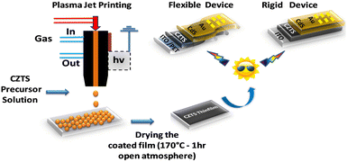 |
| | Fig. 1 APPJ printing of CZTS for the fabrication of solar cells on rigid and flexible substrates. | |
2.4. Characterization
The structural characteristics of the film were investigated using X-ray diffraction (XRD) (PANalytical X’pert powder diffractometer) with Cu Kα radiation. Raman analysis (Horiba Jobin-Yvon LabRam HR) was performed using an Ar+ laser with a 473 nm line as the excitation source. Silicon was used to calibrate the instrument at 520.7 cm−1. UV-visible spectroscopy was carried out using JASCO UV-vis spectrophotometer. The composition and surface morphology of the film were studied by SEM-EDS (Zeiss Supra 55-VP FEGSEM). Elemental analysis was performed using X-ray photoelectron spectroscopy (Kratos XSAM 800), equipped with a dual-anode X-ray source, where Mg Kα (1253.6 eV) was used for these studies. A transmission electron microscopy (TEM) study of the as-prepared sample was carried out using the JEOL JEM-2100. The semiconducting properties were studied using a Hall effect setup (Ecopia HMS Ver 3.51:3). The J–V (current density–voltage) characteristics of the devices were measured using a Keithley 2400 source-measure unit. To obtain the 1 sun AM 1.5G illumination, an Oriel Sol3A Class AAA solar simulator was employed.
2.5. Device fabrication and testing
The ITO-coated glass substrate (8–12 Ω cm−2) was ultrasonicated for 10 min in DI water, ethanol, and isopropanol (IPA), and then dried with nitrogen gas. The precursor solution of CZTS was then deposited onto the ITO substrate using APPJ. A 60 nm CdS layer (n-type) was deposited via spin coating onto the CZTS film.42 Then, using a shadow mask, Au top contacts (∼100 nm thick) were thermally evaporated under vacuum (10−6 torr). The device active area was 0.24 cm2. A similar procedure was followed for the fabrication of the device on PET/ITO substrates.
3. Results and discussion
The structural and chemical analyses of APPJ-printed and dip-coated CZTS films were performed while optimizing the precursor solution concentration and processing conditions. Raman analysis clearly showed that a few secondary phases, such as CuSnS and CuS, were present in the film APPJ-printed using the as-prepared precursor solution (Fig. S4a, ESI†). Annealing trials were conducted at (i) 130 °C and (ii) 170 °C for 1 h in open atmosphere. No secondary phases were observed in the film prepared using the 50% diluted solution and annealed at 170 °C for 1 h (Fig. S4(b), ESI†). As shown in Fig. 2(a), the XRD pattern of the APPJ-printed CZTS film dried at 170 °C for 1 h showed major peaks at 2θ = 56.1°, 47.3°, and 28.5°, corresponding to the (312), (220), and (112) planes of the kesterite CZTS phase, respectively.56 The calculated crystallite size was ∼0.32 nm along the (112) plane,57 which was close to values reported in the literature and was further confirmed by the TEM results (Fig. 4). The formation of the CZTS film was confirmed by the Raman spectrum shown in Fig. 2(b). The spectrum showed an intense peak at 338 cm−1, along with a shoulder at 287 cm−1, both corresponding to the CZTS phase. The XRD and Raman spectra revealed that the initial phase of CZTS growth was likely amorphous, as the process occurs at a relatively low temperature of 170 °C for 1 h. Moreover, the UV-visible absorption spectra of the APPJ-printed film showed absorption in the visible region (Fig. S6 and S8, ESI†), with a calculated optical bandgap of 1.50 eV. This bandgap value was in good agreement with literature reports on CZTS.56 Notably, The APPJ-printed CZTS film exhibited a higher absorption coefficient compared to the dip-coated CZTS film (Fig. S8, ESI†), possibly due to differences in crystallite size and improved microstructure.
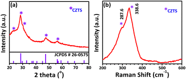 |
| | Fig. 2 (a) XRD spectrum and (b) Raman spectrum of the APPJ-printed CZTS film processed with optimized conditions. | |
Fig. 3 shows the optical and FESEM images of the APPJ-printed CZTS film. The surface of the film was more compact and denser compared to the film prepared via the dip-coating route (Fig. S5, ESI†). This could be attributed to the smaller particle size of the APPJ-printed CZTS film (∼250 nm) compared to that of the dip-coated CZTS film (∼550 nm). Furthermore, the chemical composition estimated from EDS analysis was close to the expected stoichiometry of CZTS. Interestingly, the TEM image of the APPJ-printed CZTS film sample revealed a sheet-like structure, as shown in Fig. 4(a). A similar flake-like structure was also observed in the TEM image of the dip-coated CZTS sample (Fig. S7, ESI†). The SAED patterns in Fig. 4(b) and Fig. S7(b) (ESI†) confirmed the crystalline nature of the APPJ-printed and dip-coated CZTS films. HRTEM images further confirmed interplanar spacings of 0.36 nm (APPJ-printed CZTS) and 0.32 nm (dip-coated CZTS), corresponding to the (112) planes of tetragonal CZTS (Fig. 4(c) and Fig S7(c), ESI†). Upon measuring the charge carrier density of these films using Hall Effect, the plasma-printed CZTS films exhibited p-type semiconducting behavior. The estimated carrier mobility of the APPJ-printed CZTS film was higher than that reported in earlier studies and higher than that of the dip-coated CZTS film,58–60 as it was more porous and compact (Fig. 4(b)). Interestingly, the carrier concentration and Hall coefficient were also higher compared to previous works58–60 (Table 1). The observed resistivity was slightly lower than that of the dip-coated film, which may be attributed to the improved crystallinity and density of the APPJ-printed CZTS.31
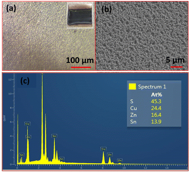 |
| | Fig. 3 (a) Optical image (inset: Photograph of the CZTS film), (b) FESEM image, and (c) EDS analysis of the APPJ-printed CZTS film. | |
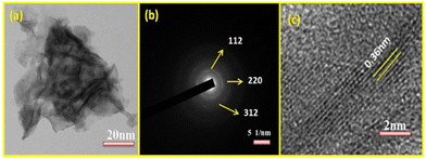 |
| | Fig. 4 (a) TEM image, (b) selected-area electron diffraction (SAED) pattern, and (c) HRTEM image of the APPJ-printed CZTS film. | |
Table 1 Hall effect measurement results of the CZTS thin film compared with those from other literature
| Method |
Carrier concentration (ρ) cm−3 |
Mobility (μH) cm2 V−1 s−1 |
Hall coefficient (RH) cm3 C−1 |
Resistivity (ρ) Ω cm−1 |
Conductivity type |
Ref. |
| Atmospheric plasma |
4.8 × 10²⁰ |
5.8 |
8.8 × 10³ |
1.1 × 10⁻² |
p |
This work |
| Dip-coating |
2.7 × 10²⁰ |
3.2 |
8.0 × 10³ |
1.2 × 10⁻² |
p |
This work |
| Doctor blade |
1.24 × 10¹⁶ |
16.57 |
30.22 |
— |
p |
58
|
| Plasma-assisted co-evaporation |
2.6 × 10¹⁹ |
2.3 |
— |
1.0 × 10⁻¹ |
p |
59
|
| dc sputtering |
2.5 × 10¹⁹ |
1.2 |
2.4 × 10⁻¹ |
1.8 × 10⁻¹ |
p |
60
|
The wide scan survey XPS spectrum of the APPJ-printed film confirmed the presence of all elements expected for CZTS (Fig. S9, ESI†). From the XPS analysis, the binding energies of 934 eV for Cu 2p3/2 and 954 eV for Cu 2p1/2, with a 20 eV peak splitting, are shown in Fig. 5(a). At higher binding energies, no satellite peaks were observed, indicating that the Cu2+ present in the starting material of CZTS had been reduced to monovalent copper. Fig. 5(b) shows the peaks at 1024 eV for Zn 2p3/2 and 1046.7 eV of Zn 2p1/2, with a 22.7 eV peak splitting. These values corresponded well with the standard divalent Zn(II) splitting. The two peaks at 487.6 eV and 496 eV, with a wide peak splitting of 8.4 eV, were attributed to the oxidation of Sn2+ in the starting material to Sn4+ (Fig. 5(c)). The two peaks located at 162.3 eV and 163.6 eV (Fig. 5(d)) were assigned to the S 2p core levels in the sulfide phases, which typically appear in this region according to the literature.61
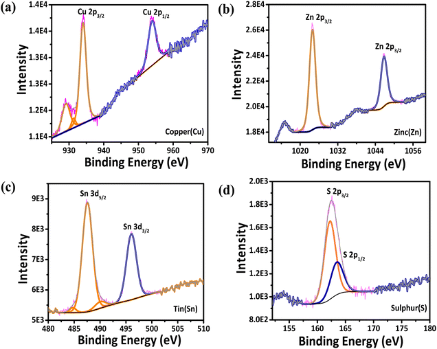 |
| | Fig. 5 XPS Spectra of (a) Cu 2p, (b) Zn 2p, (c) Sn 3d. and (d) S 2p spectra of the APPJ-printed CZTS film. | |
3.1. Heterojunction device fabrication and characterization
Simple heterojunction solar cells were fabricated with both APPJ-printed and dip-coated CZTS films in the configuration ITO/CZTS/CdS/Au, using rigid glass and flexible PET substrates. The J–V characteristics of the APPJ-printed CZTS solar cell device under light illumination are shown in Fig. 6. The device on the rigid substrate exhibited a PCE (η) of 3.1%, a short-circuit current density (Jsc) of 14.5 mA cm−2, an open-circuit voltage (Voc) of 0.47 V, and a fill factor (FF) of 0.46. The solar cell on the flexible PET substrate exhibited a η of 1.1%, a Voc of 0.37 V, a Jsc of 7.5 mA cm−2, and an FF of 0.41. In comparison to earlier reports on low-temperature processed CZTS-based solar cells, the efficiency of the APPJ-printed CZTS was superior, with a high value of Jsc (Table 2). This could be attributed to the enhanced light absorption, porous nature, and mobility, as confirmed through characterization techniques (UV visible spectra, XRD spectra, and Hall measurements). The J–V curves of the dip-coated CZTS-based solar cells on rigid and flexible substrates, measured under both dark and light illumination, are shown in Fig. S10 (ESI†). The Voc was slightly lower than that of the dip-coated CZTS film, indicating relatively more charge recombination in the APPJ-printed CZTS. This was plausible, as recombination was directly proportional to the carrier concentration, which was found to be higher in the APPJ-printed CZTS film compared to the dip-coated film (Table 2).
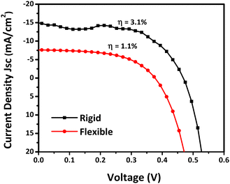 |
| | Fig. 6
J–V curves of the APPJ-printed CZTS-based solar cells on rigid and flexible substrates, measured under light illumination (100 mW cm−2, AM 1.5). | |
Table 2 Comparison of photovoltaic characteristics of heterojunction devices based on low temperature processed CZTS films
| Device structure |
Coating method of CZTS film |
Processing conditions of CZTS film |
V
oc (V), JSC (mA cm−2), FF |
η (%) |
Device area (cm2) |
Ref. |
| Pl/Mo/CZTS/CdS/ZnO:Al/Al |
Screen printing |
Drying for 1 h (open air), hot pressed using a hot roll at 195 °C (open air) |
0.38, 4.76, 0.27 |
0.49 |
0.15 |
31
|
| SLG/ITO–CZTS–PCBM–Ca/Al |
Spin-coating |
Drying in open air (temperature not mentioned) |
0.39, 5.30, 0.43 |
0.90 |
0.04 |
62
|
| SLG/FTO/TiO2/CdS/CZTS/Graphite |
Spray pyrolysis |
Drying at 140 °C for 30 min (N2) and annealed at 300 °C for 30 min (N2) |
445, 6.7, 37.4, 0.43 |
0.43 |
— |
63
|
| SLG/FTO/TiO2/CdS/CZTS/Carbon paste |
Spray pyrolysis |
Drying at 140 °C for 30 min (N2) and annealed at 250 °C for 30 min (N2) |
502, 2.8, 36 |
0.51 |
— |
64
|
| SLG/ITO/ZnO/CdS/CZTS/Au |
Spin coating |
Drying at 150 °C for 10 min (open air) and annealed at 250 °C for 10 min (open air) |
0.67, 4.10, 0.43 |
1.20 |
0.12 |
65
|
| SLG/ITO/CZTS/CdS/Al |
Spin-coating |
Annealed at 350 °C for 5 min |
0.40, 3.56, 54.90 |
0.78 |
0.32 |
42
|
| SLG/ITO/CZTS/CdS/Al |
Dip-coating |
Drying at 130 °C for 15 min and annealing at 100 °C for 2.5 h (Ar) |
0.52, 11.2, 0.47 |
2.73 |
0.24 |
46
|
| PET/ITO/CZTS/CdS/Al |
Dip-coating |
Drying at 130 °C for 15 min and annealing at 100 °C for 2.5 h (Ar) |
0.48, 2.2, 0.71 |
0.74 |
0.24 |
46
|
| SLG/ITO/CZTS/CdS/Au |
Dip-coating |
Drying at 130 °C for 15 min (open air) and annealing at 100 °C for 2.5 h (Ar) |
0.42, 11.6, 0.49 |
2.38 |
0.24 |
This work |
| PET/ITO/CZTS/CdS/Au |
Dip-coating |
Drying at 130 °C for 15 min (open air) and annealing at 100 °C for 2.5 h (Ar) |
0.33, 5.41, 0.29 |
0.51 |
0.24 |
This work |
| SLG//ITO/CZTS/CdS/Au |
APPJ |
Annealing at 170 °C for 1 h (open air) |
0.47, 14.5, 0.46 |
3.1 |
0.24 |
This work |
| PET/ITO/CZTS/CdS/Au |
APPJ |
Annealing at 170 °C for 1 h (open air) |
0.37, 7.5, 0.41 |
1.1 |
0.24 |
This work |
Thus, this work demonstrates a one-step deposition process for CZTS using the APPJ technique. It is a low-temperature, eco-friendly approach that utilizes less toxic solvents. These unique features have the potential to drive significant advancements in the scalable, environmentally sustainable fabrication of CZTS-based solar cells.
4. Conclusion
In summary, we confirmed the open-air formation of a nanocrystalline, high-quality CZTS film on rigid as well as flexible substrates at low temperature (∼170 °C) using the APPJ printing route. In comparison with the dip-coated film annealed under an Ar atmosphere, the APPJ-printed CZTS film exhibited superior quality, a higher absorption coefficient, and higher carrier concentration. The fabricated glass/ITO/CZTS/CdS/Au and PET/ITO/CZTS/CdS/Au heterojunction solar cell devices demonstrated PCEs of 3.1% and 1.1%, respectively, which are the highest reported to date for low-temperature-processed CZTS. Demonstrated with CZTS, this new approach employing APPJ printing of the precursor solution may potentially enable the scalable, low-temperature fabrication of high-quality chalcogenide thin films for various applications, including flexible photovoltaics, thermoelectrics, and photo-electrochemical devices.
Data availability
The data supporting this article have been included as part of the ESI.†
Conflicts of interest
There are no conflicts to declare.
Acknowledgements
The authors acknowledge the grant from the International Research Exchange Scheme (IES\R2\170272), The Royal Society, UK, towards this research work. The authors also thank SRM IST, Kattankulathur, Tamil Nadu, India, The Open University, UK, DST-SERB (ECR/2015/000513) and MNRE (31/03/2014-15/PVSE-R&D) for the support and funding extended. They are grateful to IIT SAIF for extending the FESEM facility and to Dr Ramesh Babu of Bharathidhasan University, Trichy, for assistance with Hall measurements. Special thanks to the Indian National Users Program (INUP) at IISc CeNSE Bangalore for providing facilities, such as cross-sectional FESEM imaging, solar simulator, and IV measurements. M. D. thanks CSIR for the senior research fellowship.
References
- M. Graetzel, R. A. J. Janssen, D. B. Mitzi and E. H. Sargent, Nature, 2012, 488, 304–312 CrossRef CAS
 .
.
- S. E. Habas, H. A. S. Platt, M. F. A. M. van Hest and D. S. Ginley, Chem. Rev., 2010, 110, 6571–6594 CrossRef CAS .
- D. B. Mitzi, O. Gunawan, T. K. Todorov, K. Wang and S. Guha, Sol. Energy Mater. Sol. Cells, 2011, 95, 1421–1436 CrossRef CAS .
- K. Ramasamy, M. A. Malik and P. O’Brien, Chem. Commun., 2012, 48, 5703 RSC .
- H. Katagiri, K. Jimbo, W. S. Maw, K. Oishi, M. Yamazaki, H. Araki and A. Takeuchi, Thin Solid Films, 2009, 517, 2455–2460 CrossRef CAS .
- Y. Li, C. Cui, H. Wei, Z. Shao, Z. Wu, S. Zhang, X. Wang, S. Pang and G. Cui, Adv. Mater., 2024, 36, 2400138 CrossRef CAS .
- R. Nitsche, D. F. Sargent and P. Wild, J. Cryst. Growth, 1967, 1, 52–53 CrossRef CAS .
- K. Ito and T. Nakazawa, Jpn. J. Appl. Phys., 1988, 27, 2094 CrossRef CAS .
- H. Katagiri, N. Sasaguchi, S. Hando, S. Hoshino, J. Ohashi and T. Yokota, Sol. Energy Mater. Sol. Cells, 1997, 49, 407–414 CrossRef CAS .
- W. Shockley, Solid State Electron., 1961, 2, 35–67 CrossRef .
- W. Wang, M. T. Winkler, O. Gunawan, T. Gokmen, T. K. Todorov, Y. Zhu and D. B. Mitzi, Adv. Energy Mater., 2014, 4, 1301465 CrossRef .
- B. Shin, O. Gunawan, Y. Zhu, N. A. Bojarczuk, S. J. Chey and S. Guha, Prog. Photovoltaics Res. Appl., 2013, 21, 72–76 CrossRef CAS .
- Y. S. Lee, T. Gershon, O. Gunawan, T. K. Todorov, T. Gokmen, Y. Virgus and S. Guha, Adv. Energy Mater., 2015, 5, 2–5 Search PubMed .
- S. Ahmed, K. B. Reuter, O. Gunawan, L. Guo, L. T. Romankiw and H. Deligianni, Adv. Energy Mater., 2012, 2, 253–259 CrossRef CAS .
- J. J. Scragg, T. Ericson, X. Fontané, V. Izquierdo-Roca, A. Pérez-Rodríguez, T. Kubart, M. Edoff and C. Platzer-Björkman, Prog. Photovoltaics Res. Appl., 2014, 22, 10–17 CrossRef CAS .
- J. Zhong, Z. Xia, C. Zhang, B. Li, X. Liu, Y.-B. Cheng and J. Tang, Chem. Mater., 2014, 26, 3573–3578 CrossRef CAS .
- T. K. Todorov, K. B. Reuter and D. B. Mitzi, Adv. Mater., 2010, 22, E156–E159 CrossRef CAS .
- C. Steinhagen, T. B. Harvey, C. J. Stolle, J. Harris and B. A. Korgel, J. Phys. Chem. Lett., 2012, 3, 2352–2356 CrossRef CAS .
- M. H. Kumar, N. Yantara, S. Dharani, M. Graetzel, S. Mhaisalkar, P. P. Boix and N. Mathews, Chem. Commun., 2013, 49, 11089 RSC .
- G. Choudhary and H. Hansen, Chemosphere, 1998, 37, 801–843 CrossRef CAS PubMed .
- F. J. C. Roe, G. A. Grant and D. M. Milican, Nat. Publ. Gr., 1967, 216, 375–376 CAS .
- T. Schnabel, M. Löw and E. Ahlswede, Sol. Energy Mater. Sol. Cells, 2013, 117, 324–328 CrossRef CAS .
- G. Wang, W. Zhao, Y. Cui, Q. Tian, S. Gao, L. Huang and D. Pan, ACS Appl. Mater. Interfaces, 2013, 5, 10042–10047 CrossRef CAS PubMed .
- F. Liu, S. Shen, F. Zhou, N. Song, X. Wen, J. A. Stride, K. Sun, C. Yan and X. Hao, J. Mater. Chem. C, 2015, 3, 10783–10792 RSC .
- G. L. Agawane, A. S. Kamble, S. A. Vanalakar, S. W. Shin, M. G. Gang, J. H. Yun, J. Gwak, A. V. Moholkar and J. H. Kim, Mater. Lett., 2015, 158, 58–61 CrossRef CAS .
- V. Tunuguntla, W.-C. Chen, P.-H. Shih, I. Shown, Y.-R. Lin, J.-S. Hwang, C.-H. Lee, L.-C. Chen and K.-H. Chen, J. Mater. Chem. A, 2015, 3, 15324–15330 RSC .
- C. Steinhagen, M. G. Panthani, V. Akhavan, B. Goodfellow, B. Koo and B. A. Korgel, J. Am. Chem. Soc., 2009, 131, 12554–12555 CrossRef CAS PubMed .
- D. Payno, S. Kazim, M. Salado and S. Ahmad, Sol. Energy, 2021, 224, 1136–1143 CrossRef CAS .
- L. Dong, S. Cheng, Y. Lai, H. Zhang and H. Jia, Thin Solid Films, 2017, 626, 168–172 CrossRef CAS .
- Q. Tian, X. Xu, L. Han, M. Tang, R. Zou, Z. Chen, M. Yu, J. Yang and J. Hu, CrystEngComm, 2012, 14, 3847 RSC .
- Z. Zhou, Y. Wang, D. Xu and Y. Zhang, Sol. Energy Mater. Sol. Cells, 2010, 94, 2042–2045 CrossRef CAS .
- I. Becerril-Romero, L. Acebo, F. Oliva, V. Izquierdo-Roca, S. López-Marino, M. Espíndola-Rodríguez, M. Neuschitzer, Y. Sánchez, M. Placidi, A. Pérez-Rodríguez, E. Saucedo and P. Pistor, Prog. Photovoltaics Res. Appl., 2018, 26, 55–68 CrossRef CAS .
- Q. Zhao, H. Shen, K. Gao, Y. Xu, X. Wang and Y. Li, J. Mater. Chem. C, 2021, 9, 17531–17541 RSC .
- K. W. Brew, S. M. McLeod, S. M. Garner and R. Agrawal, Thin Solid Films, 2017, 642, 110–116 CrossRef CAS .
- F. Fu, T. Feurer, T. Jäger, E. Avancini, B. Bissig, S. Yoon, S. Buecheler and A. N. Tiwari, Nat. Commun., 2015, 6, 1–9 Search PubMed .
- X. Mathew, J. P. Enriquez, A. Romeo and A. N. Tiwari, Sol. Energy, 2004, 77, 831–838 CrossRef CAS .
- J. Ramanujam and U. P. Singh, Energy Environ. Sci., 2017, 10, 1306–1319 RSC .
- V. V. Satale and S. V. Bhat, Sol. Energy, 2020, 208, 220–226 CrossRef CAS .
- S. Sun, T. Salim, N. Mathews, M. Duchamp, C. Boothroyd, G. Xing, T. C. Sum and Y. M. Lam, Energy Environ. Sci., 2014, 7, 399–407 RSC .
- Z. Xu, T. Li, F. Zhang, X. Hong, S. Xie, M. Ye, W. Guo and X. Liu, Nanoscale, 2017, 9, 3826–3833 RSC .
- Z. Gao, W. Jin, Y. Li, Q. Song, Y. Wang, K. Zhang, S. Wang and L. Dai, J. Mater. Chem. C, 2015, 3, 4511–4514 RSC .
- Y. Hou, H. Azimi, N. Gasparini, M. Salvador, W. Chen, L. S. Khanzada, M. Brandl, R. Hock and C. J. Brabec, ACS Appl. Mater. Interfaces, 2015, 7, 21100–21106 CrossRef CAS PubMed .
- M. A. Islam, K. S. Rahman, F. Haque, M. Akhtaruzzaman, M. M. Alam, Z. A. Alothman, K. Sopian and N. Amin, Chalcogenide Lett., 2014, 11, 233–239 CAS .
- M. Farinella, R. Inguanta, T. Spanò, P. Livreri, S. Piazza and C. Sunseri, Energy Procedia, 2014, 44, 105–110 CrossRef CAS .
- U. Saha and M. K. Alam, RSC Adv., 2018, 8, 4905–4913 RSC .
-
M. Dhanasekar and S. V. Bhat, 2020 47th IEEE Photovoltaic Specialists Conference (PVSC), IEEE, 2020, pp. 1–3 Search PubMed.
-
M. Dhanasekar, PhD thesis, SRM University, 2020 .
- G. Cummins and M. P. Y. Desmulliez, Circuit World, 2012, 38, 193–213 CrossRef CAS .
- J. M. Hoey, A. Lutfurakhmanov, D. L. Schulz and I. S. Akhatov, J. Nanotechnol., 2012, 2012, 1–22 CrossRef .
- X. Lu, G. V. Naidis, M. Laroussi and K. Ostrikov, Phys. Rep., 2014, 540, 123–166 CrossRef CAS .
- K. Ostrikov, E. C. Neyts and M. Meyyappan, Adv. Phys., 2013, 62, 113–224 CrossRef CAS .
- A. Dey, S. Krishnamurthy, J. Bowen, D. Nordlund, M. Meyyappan and R. P. Gandhiraman, ACS Nano, 2018, 12, 5473–5481 CrossRef CAS .
- M. Bhar, A. Dey, S. Ghosh, M. A. van Spronsen, V. Selvaraj, Y. Kaliprasad, S. Krishnamurthy and S. K. Martha, Carbon, 2022, 198, 401–410 CrossRef CAS .
- M. Dhanasekar, S. Sekar and S. V. Bhat, J. Colloid Interface Sci., 2021, 599, 326–331 CrossRef CAS .
- M. Dhanasekar and S. V. Bhat, Appl. Surf. Sci., 2017, 418, 194–198 CrossRef CAS .
- S. K. Swami, A. Kumar and V. Dutta, Energy Procedia, 2013, 33, 198–202 CrossRef CAS .
- J. Wang, P. Zhang, X. Song and L. Gao, RSC Adv., 2014, 4, 27805–27810 RSC .
- D. Tang, Q. Wang, F. Liu, L. Zhao, Z. Han, K. Sun, Y. Lai, J. Li and Y. Liu, Surf. Coat. Technol., 2013, 232, 53–59 CrossRef CAS .
- Y. Li, J. Chen and J. Ma, J. Mater. Sci.: Mater. Electron., 2015, 26, 6546–6551 CrossRef CAS .
- N. Muhunthan, O. P. Singh, M. K. Thakur, P. Karthikeyan, D. Singh, M. Saravanan and V. N. Singh, J. Sol. Energy, 2014, 2014, 1–8 CrossRef .
- Y. Sun, Y. Zhang, H. Wang, M. Xie, K. Zong, H. Zheng, Y. Shu, J. Liu, H. Yan, M. Zhu and W. Lau, J. Mater. Chem. A, 2013, 1, 6880 RSC .
- S. K. Saha, A. Guchhait and A. J. Pal, Phys. Chem. Chem. Phys., 2012, 14, 8090 RSC .
- K. Tanaka, M. Kurokawa, K. Moriya and H. Uchiki, J. Alloys Compd., 2013, 571, 98–102 CrossRef CAS .
- M. Kurokawa, K. Tanaka, K. Moriya and H. Uchiki, Jpn. J. Appl. Phys., 2012, 51, 10NC33 CrossRef .
- D. Lee and K. Yong, Nanotechnology, 2014, 25, 065401 CrossRef CAS .
Footnotes |
| † Electronic supplementary information (ESI) available. See DOI: https://doi.org/10.1039/d5ma00207a |
| ‡ Current address: Department of Physics, SRM Institute of Science and Technology, Ramapuram, Tamil Nadu, India, 600089. |
|
| This journal is © The Royal Society of Chemistry 2025 |
Click here to see how this site uses Cookies. View our privacy policy here. 
 Open Access Article
 This Open Access Article is licensed under a Creative Commons Attribution-Non Commercial 3.0 Unported Licence
 *bc,
Satheesh
Krishnamurthy
*bd and
S.
Venkataprasad Bhat
*a
*bc,
Satheesh
Krishnamurthy
*bd and
S.
Venkataprasad Bhat
*a


