
 Open Access Article
 This Open Access Article is licensed under a Creative Commons Attribution-Non Commercial 3.0 Unported Licence
Advancements in high-entropy materials for electromagnetic wave absorption
Mingyue
Yuan†
a,
Alan H.
Weible†
b,
Fatemeh
Azadi
b,
Bangxin
Li
a,
Jiacheng
Cui
a,
Hualiang
Lv
 *a,
Renchao
Che
*a and
Xiaoguang
Wang
*bc
*a,
Renchao
Che
*a and
Xiaoguang
Wang
*bc
aInstitute of Optoelectronics, Laboratory of Advanced Materials, Fudan University, Shanghai 200438, P. R. China. E-mail: rcche@fudan.edu.cn; lv_hl@fudan.edu.cn
bWilliam G. Lowrie Department of Chemical and Biomolecular Engineering, The Ohio State University, Columbus, OH 43210, USA. E-mail: wang.12206@osu.edu
cSustainability Institute, The Ohio State University, Columbus, OH 43210, USA
First published on 19th November 2024
Abstract
Widespread electromagnetic (EM) interference and pollution have become major issues due to the rapid advancement of fifth-generation (5G) wireless communication technology and devices. Recent advances in high-entropy (HE) materials have opened new opportunities for exploring EM wave absorption abilities to address the issues. The lattice distortion effect of structures, the synergistic effect of multi-element components, and multiple dielectric/magnetic loss mechanisms can offer extensive possibilities for optimizing the balance between impedance matching and attenuation ability, resulting in superior EM wave absorption performance. This review gives a comprehensive review on the recent progress of HE materials for EM wave absorption. We begin with the fundamentals of EM wave absorption materials and the superiority of HE absorbers. Discussions of advanced synthetic methods, in-depth characterization techniques, and electronic properties, especially with regard to regulatable electronic structures through band engineering of HE materials are highlighted. This review also covers current research advancements in a wide variety of HE materials for EM wave absorption, including HE alloys, HE ceramics (mainly HE oxides, carbides, and borides), and other novel HE systems. Finally, insights into future directions for the further development of high-performance HE EM wave absorbers are provided.
Wider impactThis review highlights key developments in high-entropy (HE) materials, emphasizing significant advances in their application for electromagnetic wave absorption. The discussion spans HE alloys, ceramics (including oxides, carbides, and borides), and emerging HE systems. The inherent stability and synergistic interactions among the diverse elements in HE materials allow for precise control over their physical and chemical properties, offering a vast design space for optimizing electromagnetic absorption performance. These breakthroughs are crucial for advancing sustainable HE materials research, providing innovative solutions for electromagnetic wave absorption, the design of HE absorbers, and the manufacturing of advanced absorbers. By bridging the gap between fundamental science and real-world applications, this review contributes to the development of impactful strategies to mitigate electromagnetic wave pollution through state-of-the-art absorbers. |
1. Introduction
The advent of fifth-generation (5G) wireless communication technology has significantly increased electromagnetic (EM) pollution, often termed the fourth kind of pollution joining water, air, and noise.1–4 Its notably higher emission power, coupled with a lower efficiency, has substantially worsened the issue of EM pollution. This problem not only poses risks to health but also compromises the functionality of electronic devices, reducing the operational efficiency of these devices and causing economic losses in related industries. Therefore, EM pollution is a concern not just environmentally but also economically.5EM wave absorbers, which effectively turn EM waves into Joule heat, are highly sought-after materials, drawing in worldwide focus for their potential in addressing EM pollution.6–8 EM wave absorbers are typically distinguished into magnetic loss and dielectric loss types, based on their underlying attenuation mechanisms.9–11 Regardless of their classification, these materials share a unified objective: to provide effective and wide-ranging absorption capabilities, while engineered to be thin and lightweight.12 This design strategy is specifically aimed at accommodating the diverse needs of numerous microwave frequency applications, while emphasizing a thin, compact structure.
Despite notable advancements in singular-type magnetic materials, including magnetic metal alloys and ferrites and purely dielectric materials like conductive carbon and narrow-bandgap semiconductors or interface-based heterostructures, these materials still exhibit pronounced limitations. The most significant of these challenges is the difficultly to concurrently attain broadband absorption while preserving an optimal thickness. Central to this problem are the intrinsic limitations of their singular attenuation mechanisms, resulting in absorption efficacy that falls below commercial standards.
To enhance attenuation intensity, researchers have proposed a magneto-electric composite strategy to diversify the forms of attenuation.13 However, this approach inevitably led to overall magnetic or electric losses that were weaker than their individual counterparts, while adding to the complexity and cost of synthesis. As an alternative solution, it has been observed that doping single magnetic metals or materials with bi-metallic, tri-metallic, or even higher order metallic elements can precisely regulate the magnetic anisotropy and demagnetization properties of magnetic materials, significantly inducing magnetic resonance loss, promoting magnetic loss and microwave absorption.14 Meanwhile, from the perspective of dielectric loss, multi-element doping profoundly modifies the material's electronic band structure and introduces lattice distortions and defects, leading to dielectric relaxation.15 Motivated by these discoveries, high-entropy (HE) EM wave absorption materials, usually comprised of single-phase metal alloys or ceramics made from a blend of five or more metallic elements, have sparked widespread interest among researchers. Yang et al. first combined the idea of HE with microwave absorption materials and then proposed a mechanically alloyed FeCoNiCrAl high entropy alloy powder absorption material in 2016.16 A plethora of HE EM wave absorption materials including HE ceramics (mainly HE oxides, carbides, and borides) and other novel HE systems have been developed by selecting an appropriate primary crystal phase and varying the substituent elements. This has presented a way to significantly modulate magnetic and dielectric properties and has demonstrated enhanced magnetic and dielectric loss ability when compared to their original crystalline phase matrix, showing their potential as EM wave absorbers. Current strategies for developing HE EM wave absorbers are mainly focused on three main aspects. (i) For HE materials, despite comprising over five different metallic elements, the elements can be categorized into two groups: primary elements that form the crystalline phase matrix and trace elements that locally and randomly substitute the primary elements without disrupting the crystal structure of the original primary elements.17 These have experimentally shown the intricate relationship between the magnetic and electrical properties of HE materials and the variety and arrangement of their elemental composition as a key aspect of their unique characteristics. (ii) The dimension and shape of HE materials play a crucial role, as they influence the electronic states of edge atoms, noticeably affecting their capabilities in absorbing EM waves.18 (iii) The pursuit of maximum entropy through the fabrication of HE materials, a process aimed at enhancing stability, inherently leads to lattice irregularities, including slippage, defects, and dislocations. This results in localized stresses, significantly influencing the material's ability to attenuate magnetic and electric signals.19
Considering the significant advancements in HE EM wave absorption materials, there remains a notable gap in comprehensive literature, particularly in dissecting the intricate relationships among atomic types, defects, nanostructures, and EM wave absorption. This emphasizes the need for an extensive and systematic review of these materials. Our aim in writing this review is to bridge this gap by providing an in-depth analysis that encompasses the fundamentals, the interplay between composition, morphology/structure, and EM wave absorption performance. Strategies for designing, characterizing, and electronic structure-regulating HE materials are also highlighted. Importantly, the review covers current research advancements in a wide variety of HE materials for EM wave absorption, including HE alloys, HE ceramics (mainly HE oxides, carbides, and borides), and other novel HE systems (Scheme 1). Additionally, this review offers a conclusion that highlights the pressing challenges and future application prospects of HE EM wave absorption materials, addressing the critical need for such a comprehensive resource in this field.
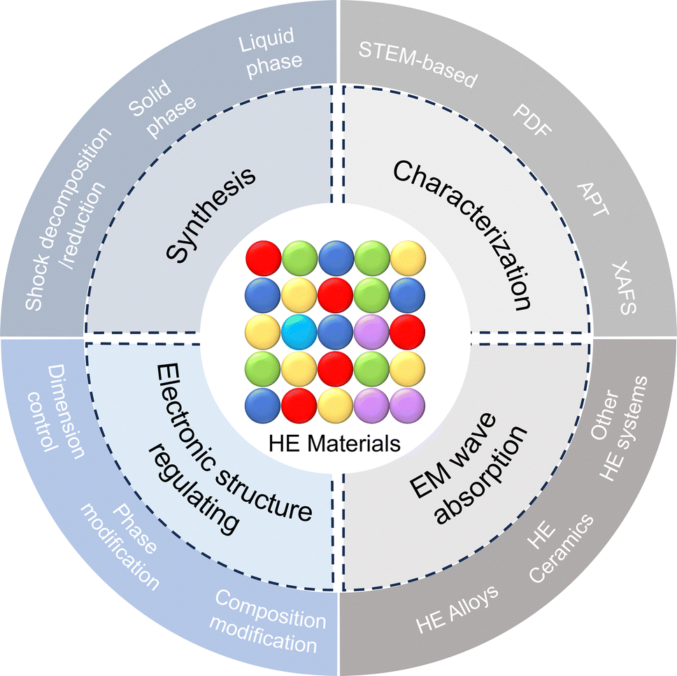 | ||
| Scheme 1 Summary of this review including synthetic methods, characterization techniques, electronic structure-regulating strategies, and electromagnetic wave absorption applications of high-entropy materials. | ||
2. HE materials and EM wave loss correlation
2.1. Mechanisms of EM attenuation
Typically, EM wave loss primarily stems from two types: magnetic loss and dielectric loss (Fig. 1).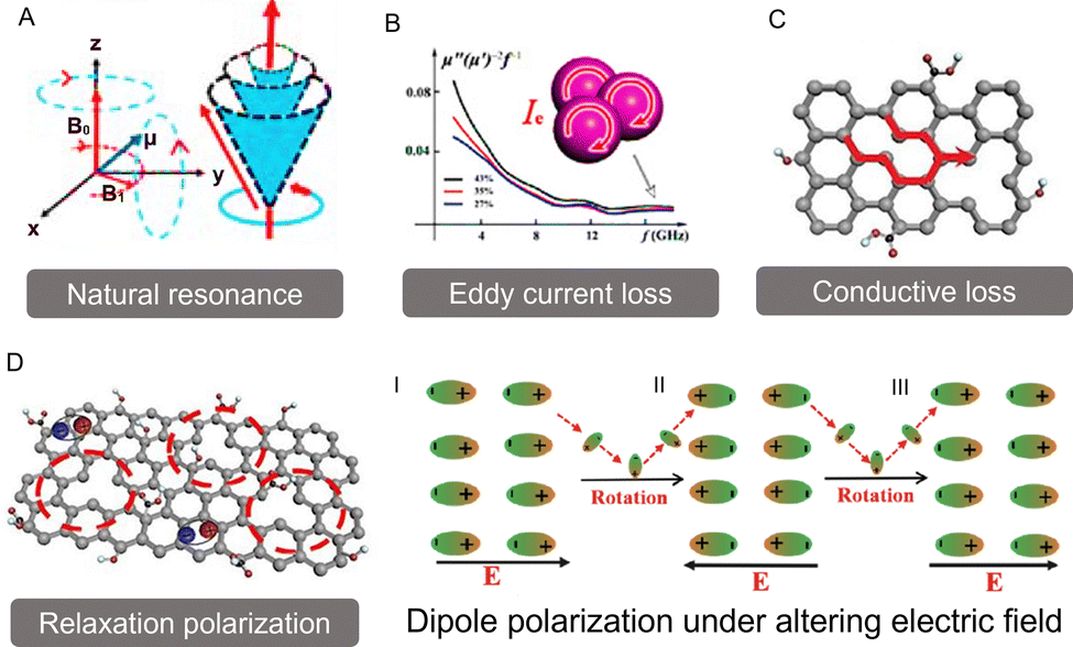 | ||
| Fig. 1 The main magnetic and dielectric loss mechanisms of electromagnetic wave absorption. (A) Natural resonance. Reproduced with permission from ref. 10. Copyright (2020) Springer Nature. (B) Eddy current loss. Reproduced with permission from ref. 20. Copyright (2022) John Wiley and Sons. (C) Conductive loss and (D) polarization relaxation. Reproduced with permission from ref. 21. Copyright (2021) Elsevier. Of particular note: the dipole polarization occurs in an alternating EM electrical field. Reproduced with permission from ref. 4. Copyright (2022) Elsevier. | ||
Eddy current loss represents a common EM phenomenon that primarily arises in magnetically conductive materials. It occurs when these materials encounter an alternating EM field, inducing circular currents—known as eddy currents—within them. These eddy currents produce their own magnetic field, which opposes and mitigates the original magnetic field (Fig. 1B). As a result, energy is dissipated in the form of heat. This interplay of magnetic fields and internally induced currents is a crucial aspect of heat generation in magnetic materials, particularly when they are exposed to changing EM environments. This nuanced interaction accentuates the dynamic nature of EM responses in such materials. Typically, eddy current loss predominantly occurs in magnetic materials with good electrical conductivity and is more pronounced in the mid- to high-frequency range, rather than in low-frequency or poorly conductive ferrimagnetic materials. This happens due to significant eddy current loss requiring a rapidly changing external magnetic field and sufficiently high electrical conductivity in the material. In general, the eddy current loss (termed as Co) is related to the diameter (D) and conductivity (σ) of the material, which can be approximately expressed as follows:27
| Co ≈ 2πμ0μ′2σD2f/3 = μ′′(μ′)−2f−1 | (1) |
 and conductive loss
  . Although both modes play a crucial role in EM loss, the key difference lies in conductive loss occurring across the entire broadband frequency range, whereas polarization loss is confined to specific narrowband segments. There exists a certain competitive relationship between these two loss mechanisms. For conductive loss, in an applied EM field, the electrical energy enables the carriers to overcome the resistance to directional flow, and the corresponding energy loss is termed conductive loss (Fig. 1C). Commonly, the conductive loss intensity has a close correlation with the conductivity (σ), based on the free-electron theory:28
 | (2) |
 can be increased by enhancing the electric conductivity. Noticeably, the conductivity reported here refers to electrical conductivity in an applied EM field, often called microwave conductivity, rather than static electric conductivity. In the microwave region (2–18 GHz), the energy of microwaves is generally insufficient to excite the carriers or quicken the migration for EM materials. Therefore, the electrical conductivity in a microwave field is almost equal to the static electric conductivity.29 Excessive conductive loss can enhance the surface reflection of EM waves, counteracting EM attenuation. Therefore, it is essential to maintain conductive loss at a moderate level.
Meanwhile, polarization relaxation is regarded as an ideal dielectric loss form as reverse radiation is not produced. Commonly,  arises from the local movement of bound charges and the variations of dipole moments in an alternating EM field (Fig. 1D). Once polarization relaxation occurs, both ε′ and ε′′ values can be affected within a relatively narrow frequency region, and thus two phenomena can be observed: a sharply decreased ε′ value, caused by a frequency dispersive effect, and a dielectric resonance peak in ε′′. With respect to the frequency dispersive effect, the plots of ε′ versus ε′′ are single semicircles, normally denoted as a Cole–Cole semicircle, according to the classic Debye theory. Specifically, the relative complex permittivity (εr) can be calculated as follows:30
 | (3) |
 | (4) |
 | (5) |
Based on eqn (4) and (5), ε′ − ε′′ can be expressed as:
| (ε′ − ε∞)2 + (ε′′)2 = (εs − ε∞)2 | (6) |
According to eqn (6), each Cole–Cole semicircle corresponds to one or more Debye relaxation processes. To discuss the polarization relaxation, the types of dipoles need to be identified first, which may result from the deformation of electron clouds, crystal defects, activated electrons towards higher energy orbitals, and so on. Although dipoles may be generated from various conditions, the response frequencies exhibit remarkable differences, which will be discussed later. For example, ionic and electronic polarization usually occurs in a lower frequency region (commonly less than the GHz band). Electronic or atomic polarizations can be induced only by an ultrahigh frequency (normally ranging in the THz band).31,32 In the microwave region, the dipoles exist on the crystal defects or interfaces of a multicomponent material system. Similarly, polarization can be either dipole or interfacial. It is believed that the interface polarization intensity is associated with the frequency and absolute electronegativity (Δη = |η1 − η2|).33 In a multicomponent material system, there are differences in the electronegativity (η), suggesting variations in the electronic attraction ability. In an alternating EM field, the electrons from the component with a lower η value accumulate in another higher η value component, leading to a capacitor-like electronic structure followed by a recovery. The EM waves can be dissipated by this periodic dynamic process. Apart from the interface polarization relaxation, crystal defects can work as dipoles in an altering electric field. These dipoles rearrange from their original orientation to align with the electric field, resulting in energy loss. Therefore, the dipoles continuously follow the electric field and are favourable to dielectric loss.
Intrinsic EM parameters can be calculated based on the following equations:34
 | (7) |
 | (8) |
2.2. Superiority of HE materials in electromagnetic wave absorption
As stated previously, HE materials are a class of single-phase metal alloys or ceramics, composed of five or more metallic elements.36,37 The defining feature of these materials lies in their elemental diversity and complexity.38 In such materials, certain elements predominantly constitute the main crystal structure, while others are present in minor quantities, locally and randomly substituting the principal elements.39–41 A distinctive characteristic of HE materials is the non-uniform distribution of elements, coupled with variations in electronegativity and atomic radii among these elements. This leads to significant differences in elemental composition, coordination, and overall electronegativity between cells, manifesting as long-range order and short-range disorder.42–44 The heterogeneity and elemental differences induce distortions between cells, increasing the likelihood of electron collision with lattice atoms, intensifying electron scattering, which affects the electronic energy levels, and potentially causing a splitting of levels, bending of energy bands, or changes in band widths. Such alterations facilitate the formation of localized energy levels or impurity levels between the conduction band and the valence band. The emergence of these new energy levels enhances the localization of electrons, endowing the material with semiconductor properties. Additionally, these energy levels significantly modulate the dielectric properties of the material, effectively balancing electrical conductivity.45 Therefore, HE materials exhibit great advantages in EM wave absorption in terms of highly modulatable conductive loss.Moreover, as mentioned above, the dipoles that exist in the multicomponent material system mainly contribute to the polarization loss mechanism in the microwave range, further promoting EM wave absorption. HE materials generally exhibit more pronounced lattice distortion and shear strain due to the lattice distortion effect. The lattice distortion in the HE grain induces their symmetry centers to deviate from the original balance points, thereby generating more intensive dipoles, which aids in increasing polarization loss under a microwave field. Additionally, HE materials possess a larger number of crystal defects or impurities compared to common single/binary element materials. For example, oxygen vacancies are more likely to be generated in HE oxides, and electrons are closely bound around the cations, leading to greater electron enrichment. This local electron abundance in metal atoms results in the formation of strong dipoles, amplifying the response to the incoming EM field and leading to an even higher polarization loss. Furthermore, HE materials tend to contain a higher concentration of stacking faults, forming more grain boundaries compared to materials without entropy regulation. For instance, the contact potential drives the directional movement of electrons and charge carriers due to the different work functions and electronegativity between the heterointerfaces inside HE materials. Electrons and charge carriers accumulate at these heterointerfaces, while the radiated reverse electric field counteracts the carrier motion, ultimately creating a capacitor-like electronic structure and forming a remarkable dipole layer. Benefiting from the periodicity of EM waves, energy is dissipated during interfacial polarization relaxation.
In HE materials, eddy current losses originate from the excitation of induced eddy currents, in response to alternating EM fields. HE materials can generally induce more beneficial eddy current losses than others due to their highly tunable electrical conductivity. From the perspective of natural ferromagnetic resonance loss in the HE materials, the distortion of crystal cells modifies the distances and angles between atoms, as well as the lattice configuration, thereby amplifying the interatomic magnetic exchange interactions and magnetic anisotropy, which strongly influence the natural ferromagnetic resonance.46–48 Meanwhile, such alterations result in the magnetic domains becoming finer, more dispersed, and irregular. Consequently, this significantly increases the resistance to the movement of domain walls, exacerbating the magnetic hysteresis phenomenon and enhancing the strength of magnetic resonance, as well as widening the frequency range of resonance, thus facilitating the broadening of the spectrum of natural magnetic resonance loss.49–51
When compared with other lower-entropy materials, HE materials offer great superiority in dielectric loss or magnetic loss, some even provide a synergistic effect of both mechanisms, and such advantages can achieve the balance between EM dissipation ability and degree of impedance matching to a maximum extent. To sum up, HE materials demonstrate immense potential in research and applications related to electronic, optoelectronic, and magnetic materials, particularly in regulating EM properties and enhancing material performance. This unique set of characteristics positions HE materials as a focal point in contemporary materials science research.52
3. Synthesis of HE materials
Conventional HE materials, often formed through thermal approaches, usually have a bulky size with a small surface area-to-volume ratio, limiting their utility in functional applications. This limitation motivated the exploratory synthesis of advanced HE micro–nanomaterials, which has highlighted the importance of continually improving the EM wave absorption efficiency. Until recently, synthesis methods of advanced HE materials can be classified into three main categories: shock decomposition/reduction synthesis, solid phase synthesis, and liquid phase synthesis.3.1. Shock decomposition/reduction synthesis
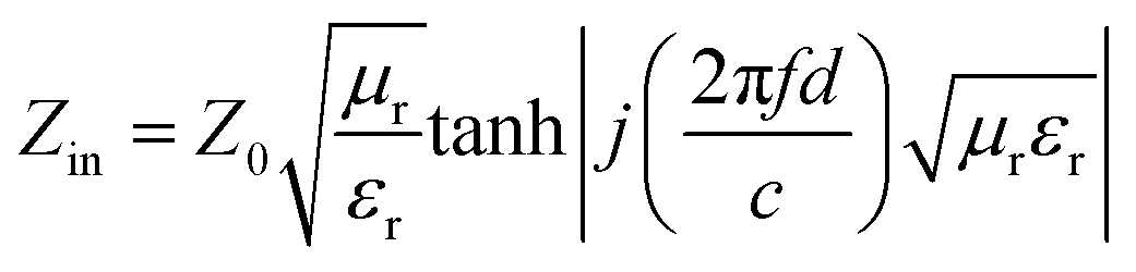
A common strategy for synthesizing advanced HE materials is through shock decomposition/reduction of mixed metal precursors. Shock decomposition/reduction techniques mainly rely on a nonequilibrium process, such as the carbothermal shock technique (CST) and fast-moving bed pyrolysis.53,54 The thermodynamically favourable HE phases are kinetically trapped during the ultrafast heating–cooling process. The short growth time, in the scale of seconds or less, ensures the formation of nanosized particles with enlarged surface areas.CTS was first reported by Yao et al. who incorporated multiple elements into octonary HE PtPdCoNiFeCuAuSn nanoparticles (NPs) using thermal shock at ∼2000 K, for ∼55 ms, at a heating rate of ∼105 K s−1.53 As shown in Fig. 2A, the CTS process involves two steps: (i) the required metal precursor formulations are formed in a solution phase based on the combination and composition of the alloy NPs; (ii) the precursors are loaded onto a carbon support and are applied with a rapid thermal shock, followed by fast quenching. During the thermal shock and fast quenching processes, the precursors (metal salts) on the carbon support undergo decomposition and alloy formation. Hence, this process overcomes the immiscibility of the elements by forming liquid alloys with uniform mixing of the elements at high temperatures. Notably, the carbon used for the support is usually defective in order to maintain a uniform size and dispersion density of the alloy NPs. This enhancement in performance of the NPs prepared by CTS is attributed to: (i) the shorter synthesis time (few milliseconds, <1 s), involving ultrafast heating and rapid cooling that freezes solid solutions to form NPs; (ii) the use of a defective carbon substrate (aids in anchoring NPs to defective sites) and interactions between them lead to strong binding and the prevention of depleting the NPs leading to stability enhancement by inhibiting coarsening and aggregation, even at longer durations and high temperatures; and (iii) enhanced configurational entropy originating from multiple elements (4–8 elements), leading to a low Gibbs free energy resulting in stable, promising catalysts. Cui et al. reported the synthesis of (CrMnFeCoNi)Sx HE metal sulfides via CST in the presence of thiourea, suggesting that this method is not only limited to the synthesis of HE alloys.55 Therefore, this process can be further explored for future EM applications.
 | ||
| Fig. 2 Representative synthesis of high-entropy materials. (A) Schematic illustrating the carbothermal shock technique synthesis of the high-entropy alloy nanoparticles (upper left) and temperature evolution during the rapid heating–cooling process (upper right). Individual and low-magnification high angle annular dark field scanning transmission electron microscope images with energy-dispersive X-ray spectroscopy element maps of octonary (PtPdCoNiFeCuAuSn) nanoparticles. Scale bar, 10 nm (lower left). Atomically resolved high-angle-annular-dark-field scanning transmission electron microscope image with the fast Fourier transform pattern showing the fcc structure (lower right). Reproduced with permission from ref. 53. Copyright (2018) The American Association for the Advancement of Science. (B) Schematic diagram of the moving bed pyrolysis method and the synthesis of high-entropy alloy nanoparticles by fast-moving bed pyrolysis and fixed bed pyrolysis strategies. Reproduced with permission from ref. 54. Copyright (2020) Springer Nature. (C) Schematic illustration of the ultrasonication-assisted wet chemistry method. Reproduced with permission from ref. 56. Copyright (2019) John Wiley and Sons. (D) Current transient corresponding to the collision of a single nanodroplet onto a carbon fiber ultramicroelectrode (left) and a representation of a nanodroplet collision event (right). Reproduced with permission from ref. 57. Copyright (2019) Springer Nature. | ||
However, the CTS approach requires the support materials to be highly electrically conductive, limiting its potential application to a certain extent. Fast-moving bed pyrolysis eliminates the need for conductive supports while enabling the synthesis of nanosized HE particles. Gao et al. developed a fast-moving bed pyrolysis method to prepare HE alloys with diverse supports. To achieve this, metal precursors were impregnated onto the support, dried, and placed into a pre-heated furnace for annealing under an inert atmosphere. Mixed metal precursors were rapidly heated to ∼923 K (higher than their pyrolysis temperature) within 5 s. With this strategy, quinary FeCoPdIrPt, senary AuPdPtCuNiSn, octonary AuIrPdPtCoCuNiSn, and denary AuIrPdPtRhCoCuMnNiSn HE alloy NPs were successfully synthesized, and exhibited high mass activity and stability (Fig. 2B).54
Additionally, lasers have been used as a high-energy shock source enabling the rapid formation of HE materials. Wang et al. adapted the kinetically-controlled laser ablation method for the synthesis of supported PtIrCuNiCr and PtAuPdFeNi HE alloy NPs.58 Additional treatment of the loaded mixed metal chloride materials with sodium hydroxide, borohydride, ammonium chloride, or triphenyl phosphine, prior to laser ablation, resulted in the synthesis of HE oxides, borides, nitrides and phosphides, respectively, highlighting the versatility of this method for the synthesis of a wide variety of HE materials. However, the productivity of these shock decomposition/reduction techniques is very low. Future work to enhance the productivity for industrial applications is needed. Besides the effectiveness and productiveness, these rapid shock methods often require specialized and sophisticated facilities that are not easily accessible to general researchers, emphasizing the need for developing simpler synthesis protocols.
3.2. Solid phase synthesis
Solid phase synthesis is the technique that achieves atomic mixing of different species by creating local extreme solid phase environments. This process involves several steps including pre-annealing mixing, such as mechanical ball milling to produce an even elemental mixture, followed by high-temperature calcination.59 Generally, re-mixing and re-calcination steps are required to improve the elemental homogeneity in the HE materials. In the mechanical ball milling process, the strong forces produced by collision and friction between the balls and the container wall generates high energy capable of not only modifying the morphology of materials but can also trigger chemical reactions. It is worth mentioning that the overall operating conditions of these methods still remain mild, thus benefiting scale-up implementations.Tailoring the ball milling parameters (e.g., temperature and time) enables tuning of the materials’ properties, such as the particle size, the morphology, or the phases present. The first report of HE boride synthesis included (Hf,Nb,Ta,Ti,Zr)B2, (Hf,Mo,Ta,Ti,Zr)B2, (Hf,Mo,Nb,Ti,Zr)B2, (Hf,Mo,Nb,Ta,Ti)B2, and (Mo,Nb,Ta,Ti,Zr)B2 which were produced using high-energy ball milling of individual commercial diboride powders, followed by spark plasma sintering at 2000 °C.60 HE metal oxides and fluorides were also synthesized through high-energy ball milling of their constituent metal oxides or metal fluorides, establishing ball milling as a versatile, easily-scalable, and cost-effective technique.61,62 One drawback of this method is that the particle sizes of the solid-state reagents are generally above 100 nm, which inhibits elemental mixing at the nanoscale prior to the annealing process, which often leads to the requirement of energy-intensive (usually above 1000 °C) and time-consuming (generally between 10 h and 24 h) procedures to ensure sufficient elemental distribution at the nanoscale.
3.3. Liquid phase synthesis
Liquid phase synthesis refers to a wet-chemistry method that utilizes external factors in the liquid phase, such as solvent and ligand molecules in colloidal and polyol solutions, to facilitate the formation of nanoscale HE materials at relatively low temperatures (usually 160–300 °C). The morphology of the final product can be controlled by adjusting the reaction temperature and reagent concentrations. Surface capping ligands can modify the energetic barrier for homogeneous nucleation and growth, yielding HE nanocrystals instead of phase-segregated heterostructures.63,64For traditional liquid phase synthesis strategies, it is common to use a solvothermal method followed by annealing. Wang et al. obtained a HE (CoCuFeMnNi)3O4 spinel oxide with one of the smallest nanometer sizes (≈5 nm) achieved thus far for HE oxides. The use of liquid-phase precursors was the key to attaining the high dispersion of five transition metal cations at the molecular level.65 Lai et al. prepared a gel containing five kinds of metal species (Fe, Co, Ni, Cr and Mn) and phosphorous species through a sol–gel method, and successfully prepared HE NPs by calcining the obtained gel precursors at high temperature.66 Spiridigliozzi et al. demonstrated the applicability of co-precipitation by preparing a library of 18 different rare earth HE oxides through a simple, scalable method by mixing an aqueous solution containing metal nitrate precursors with an ammonia solution, followed by annealing in air at 1500 °C.67 Liu et al. developed a facile ultrasonication-assisted wet-chemistry method for preparing HE alloy NPs (Fig. 2C). The local temperature of the ultrasonication cavities is expected to reach extremely high temperatures, up to 5000 °C, directly accelerating the reduction of metallic ions to form an entropy-maximized state, facilitating the formation of HE alloys.56
Another solution-based method that can be used to prepare HE alloys is nanodroplet-mediated electrodeposition. A microemulsion, generated for example by ultrasonicating a mixed solution of dichloroethane and water containing the metal precursor salts, is directed towards an electrode under a cathodic potential (Fig. 2D). Metal precursors confined within the nanodroplets are reduced by an electric shock (ca. 100 ms) when in contact with the electrode surface, resulting in the corresponding HE alloy formation.57 Wu et al. utilized a polyol reduction strategy to synthesize a noble metal-based IrPdPtRhRu HE alloy with a 5.5 nm particle size and a narrow size distribution. An aqueous solution containing the metal precursors was added to a pre-heated triethylene glycol solution with PVP at 230 °C.68 A more traditional approach to prepare metal NPs is through chemical reduction using a strong reducing agent such as sodium borohydride. This method was adapted by Feng et al. for the synthesis of a 2 nm NiCoFePtRh HE alloy supported on carbon.69
Cation exchange methods in the liquid phase have been reported to synthesize nanoscale HE metal sulfides. McCormick et al. suspended prefabricated roxbyite copper sulfide (Cu1.8S) nanoparticles in solutions containing appropriate amounts of various metal chlorides which exchange with Cu to form (ZnCoCuInGa)S HE metal sulfide NPs. This method is entropically favorable as the cation exchange reaction occurs in solution, which is advantageous for the formation of HE materials. However, this approach is potentially unscalable as the relatively slow diffusion rate (estimated to be approximately 115 days to diffuse 100 μm) would preclude bulk HE metal sulfide formation.70 Furthermore, liquid phase synthetic techniques via molecular precursors have significant advantages, including homogenous mixing of the precursors at the atomic scale, maximizing the disorder and thus entropic stabilization occurs in the solid-state products, prefabricated chemical bonds in the precursors, enabling relatively reduced synthesis times (1–5 h), and relatively low preparation temperatures (300–500 °C) compared to other synthetic approaches.71,72
An alternative synthetic route combining both solid and liquid phases can also be effective. Recently, a novel two-dimensional HE metal dichalcogenide (MoWReMnCr)S2 was fabricated with a combination of ‘bottom-up’ and ‘top-down’ approaches.73 The bulk HE material was initially synthesized through solventless thermolysis of a mixture of five individual metal dithiocarbamate precursors at 500 °C for 1 h. The structural similarity between the as-prepared HE disulfide and layered 2H-MoS2 enabled liquid-phase exfoliation to extract a few layered HE (MoWReMnCr)S2 nanosheets (3–7 atomic layers). The few layered nanosheets produced contained a homogeneous elemental distribution of metals at the atomic scale. Overall, these approaches can potentially extend to the synthesis of manifold HE chalcogenides due to the wide library of available transition metal, main group, and lanthanide single source precursors.
With the development of HE materials, more researchers are paying attention to the morphological and structural regulation in the synthesis process. Lai et al. proposed a universal precursor oxidation method to simultaneously achieve the synthesis and regulate the structure of HE oxides.74 Different metal sources are uniformly integrated into amorphous carbon spheres through a hydrothermal process. The resulting carbon spherical precursor is transformed to crystalline HE oxides after an oxidation process. By controlling ion diffusion and oxidation rates, HE oxides with different structures, including solid, core–shell, and hollow spheres, can be controllably achieved. The construction of porous structures can not only increase the specific surface area and accessibility of polarization sites, but also facilitate the impedance matching with air, which is highly desired for EM wave absorption.75 Chemical and electrochemical dealloying was shown to be an effective ‘top-down’ approach in preparing HE materials with a nanoporous structure.76–78 This is typically attained by combining different metal constituents with a diluent phase, such as aluminium (Al), using a conventional metallurgy method, followed by chemical or electrochemical etching, leading to the final HE materials with the desired composition. Jin et al. recently reported the synthesis of Al96Ni1Co1Ir1X1 and Al96Co1Fe1Ni1X1 (X = Mo, Cr, Cu, Nb or V) ribbons by melting individual metals in an arc-melting furnace under Ar protection followed by melt spinning. The excess Al was then chemically etched, or dealloyed, with 0.5 M sodium hydroxide to obtain the corresponding nanoporous HE materials. These HE materials are generally mechanically robust and possess hierarchical macro- and meso-pores.79
4. Advanced characterization techniques for HE materials
4.1. Scanning transmission electron microscopy (STEM)-based characterization
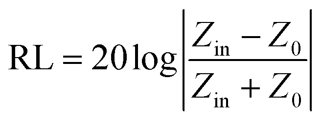
Advanced electron microscopy technology is needed to better understand the particle size, morphology, and distribution of each element in HE materials. Transmission electron microscopy (TEM) relies on the interaction between electrons and samples and is widely used to obtain local information such as the morphology and size of materials. TEM has the features of a large depth of field, high resolution, intuitive imaging, strong stereo sense, wide magnification range, and allows the sample to be rotated and tilted in three-dimensional space. STEM can be used for the visualization and analysis of the HE structures and fine details of the chemical components at the nano scale. In recent years, with the introduction of spherical correction, the spatial resolution of STEM has reached the level of sub-angstrom, and imaging observation of a single atomic column can be achieved. Furthermore, in addition to local structures, STEM combined with various techniques—such as energy dispersive X-ray spectroscopy (EDS), electron energy loss spectroscopy (EELS), and geometric phase analysis (GPA)—expand STEM's functionality. The broader functionality allows for the clarification of local chemical compositions and plays a crucial role in assessing the structural homogeneity of HE materials (Fig. 3A). | ||
| Fig. 3 Representative characterization techniques of high-entropy materials. (A) Schematic summarizing the various characterization techniques of high-entropy materials. (B) Magnification of local regions in the atomic scanning transmission electron microscopy-energy dispersive X-ray spectroscopy mapping of CrMnFeCoNi Cantor alloy. Reproduced with permission from ref. 80. Copyright (2019) Springer Nature. (C) Scanning transmission electron microscope image with electron energy loss spectroscopy line scan location with the colour corresponding to the region of the electron energy loss spectroscopy spectra (left) and monochromatic electron energy loss spectroscopy core loss edge spectra of Mn for (Mg0.167Ni0.167Co0.167Cu0.167Zn0.167Mn0.167)O (right). Reproduced with permission from ref. 81. Copyright (2023) Oxford University Press. (D) I: Inverse fast Fourier transform image taken along the [112] zone axis, II: εxx and III: εyy for (Zr0.2Ce0.2Hf0.2Y0.2Al0.2)O2-δ. Reproduced with permission from ref. 82. Copyright (2023) Elsevier. (E) I: Scanning transmission electron microscope images of the irradiation-induced layers in a (ZrHfTiSn)O2 ceramic, II: the magnified surface regions of image I, where the insets are the high-resolution transmission electron microscope image of the local region of II and the corresponding fast Fourier transform image, III: the corresponding selected area electron diffraction patterns. Reproduced with permission from ref. 83. Copyright (2023) John Wiley and Sons. (F) X-ray pair distribution function modelling of HEREZ-Tb data. Reproduced with permission from ref. 84. Copyright (2021) John Wiley and Sons. (G) Extended X-ray absorption fine structure spectra of CoZnCuNiFeZrCeOx. Reproduced with permission from ref. 85. Copyright (2022) American Chemical Society. (H) Atomic probe tomography images showing the elemental distribution and multicomponent nature in the L12 type high-entropy intermetallic. Reproduced with permission from ref. 86. Copyright (2020) John Wiley and Sons. | ||
STEM combined with EDS not only provides high-resolution images of individual particles, but also shows detailed information about the elemental distribution through a two-dimensional projection of a particle, which are more commonly applied to HE alloys because of their high sensitivity toward metallic elements with higher atomic numbers. Ding et al. displayed high angle annular dark field-scanning transmission electron microscope (HAADF-STEM) images and EDS maps of the HE CrMnFeCoNi alloy.80 On each EDS map for a specific element such as Cr, the brightness of an individual spot increases with the number of Cr atoms in the atomic column along the [110] zone axis and represents the local Cr density. As shown in the EDS maps in Fig. 3B, some random density variations can be seen for all five elements, but Co, Cr, and Ni share a more similar degree of homogeneity than Fe and Mn.
Elemental diagrams of STEM combined with EELS can specify the local chemical composition, which is important for evaluating the structural uniformity of HE materials.19,87–89 EELS can be used to identify the oxidation state of the target element and can more sensitively detect light elements such as C, N and O. Ayyagari et al. performed STEM-EELS measurements to understand the oxidation state distribution of transition metals within a HE (Mg0.167Ni0.167Co0.167Cu0.167Zn0.167Mn0.167)O film. From the EELS core loss edge spectra (right) in Fig. 3C, the energy onset of the L2, L3 core loss edge of Mn and Co ions across the thin film was observed. This local variation in valency is speculated to be due to the strain in the thin film as it is grown epitaxially on an MgO substrate.81
Wen et al. used a STEM-based inverse fast Fourier transform (IFFT) image and GPA to characterize the lattice dislocations in a HE fluorite oxide (Zr0.2Ce0.2Hf0.2Y0.2Al0.2)2-δ at the nano-to-atomic scale.82 I in Fig. 3D is the IFFT image taken along the [112] zone axis of (Zr0.2Ce0.2Hf0.2Y0.2Al0.2)2−δ. As shown by the red dashed circles, it can be clearly observed that there are no obvious defect structures, but the lattice fringes exhibit distortions implying the presence of lattice distortion.
GPA is a widely used method to map the strain field from high resolution STEM images based on Fourier space-based data processing and has been applied with various HE materials. Combining STEM with GPA, strain quantification can be achieved with both high precision and a large field of view.90–93 II and III in Fig. 3D indicate varying values in strains εxx and εyy and alternating positive and negative values in strain maps without significant aggregation. With the crystal structure being free of defects, εxx and εyy strains are mainly distributed within ±4%.82
HAADF-STEM coupled with fast Fourier transform (FFT) analysis can reveal the atomic arrangements.83 He et al. studied the influence of ion irradiation on intrinsic lattice stress and phase transition of HE orthorhombic (ZrHfTiSn)O2 ceramics. Fig. 3E depicts the STEM images as well as the corresponding FFT patterns of the damaged layers along with the magnified specific regions. According to the STEM images, a two-layered irradiation damage feature formed on the sample surface, composed of a 30 nm thick amorphous layer and a ∼100 nm thick mixed layer. In the mixed layer, it was very difficult to distinguish visually between the amorphous and crystalline regions. The FFT analysis of the crystalline region in the mixed layer revealed that the small crystalline area underneath the continuous amorphous layer had a triclinic lattice structure.
4.2. Pair distribution function (PDF) analysis
In recent years, PDF has become an increasingly popular method for probing the atomic-level structure of disordered materials. The PDF method is sensitive to the chemical properties of O-containing species and the coordination around O in the local structure. By measuring the intensity of high-energy X-rays, neutrons, or electrons scattered from a sample at various angles, functions generate that describe the probability of locating two atoms at a particular distance within the material. PDF analysis makes use of the entire spectrum, including both Bragg and diffuse scattering. In contrast to the refinement of structures based on conventional diffraction data where only primitive unit cells are typically considered, modelling PDF data often requires the use of large supercells to account for the wide range of coordination environments that may exist.94,95To explore the local structure of HE rare-earth zirconates (HEREZs, nominal composition RE2Zr2O7 with rare-earth (RE) element combinations including Eu, Gd, Tb, Dy, Ho, La, and Sc), synchrotron X-ray PDF measurements were performed (Fig. 3F).84 The three HEREZ samples exhibit similar PDF features, with exception of their high radius of ion (r) amplitudes caused by differences in crystallinity. The PDF analysis indicates that the local atomic structure departs strongly from the average fluorite lattice and is similar in all compositions studied. The finding of the variations in the radius of ions with different valence state (r3+/r4+) ratios and synthetic methods had remarkably little impact on the resulting local atomic structures within the HEREZ series, supporting the notion that high configurational entropy promotes random cation distributions and significant local bonding distortions within the RE2Zr2O7 lattice.
4.3. X-ray absorption fine structure (XAFS)
XAFS includes a diverse family of spectroscopic techniques, such as X-ray absorption near edge structure (XANES) and extended X-ray absorption fine structure (EXAFS). When the spectral peak and shoulder of more than 20 to 30 eV are passed through the edge, the XANES region appears. The fine structure on the high-energy side of the edge, where the energy decays to a few hundred electron volts, is called EXAFS. Additionally, XANES is caused by the multiple scattering of excited photoelectrons by the surrounding atoms. It not only reflects the geometric configuration of atoms in the surroundings of the absorbing atoms, but also reflects the structure of electron states in the low energy region near the Fermi level, so it becomes a useful tool for studying HE materials.Tan et al. confirmed the severe oxidation of Mn in a CrMnFeCoNi HE alloy by analyzing XANES spectra.96 In addition, XANES showed that Ni, Co, and Fe atoms maintained similar crystal structures in the alloy, but the local short-range environment was slightly different. EXAFS can be used to study the coordination structure of atoms in HE alloys and the chemical bond parameters between macromolecules. The production of EXAFS spectra is related to the scattering of absorbing atoms and the surrounding atoms, that is, they are all structure dependent. The main feature of the EXAFS method is that it can measure different kinds of atoms respectively, give the nearest neighbour structure of a specified element, and distinguish the identities of the nearest neighboring atoms. It is also possible to use strong X-ray sources to study the neighbouring structures of atoms in very small quantities and study both ordered and disordered matter. Liu et al. proved that there are certain differences among the elements Co, Zn, Cu, Ni, Fe, Zr, and Ce in HE materials through EXAFS spectra (Fig. 3G).85 There are obvious differences in the relative strength, coordination number, and bond distance of each metal element in the EXAFS curves, which reveal the different local structures and chemical environments of each element.
4.4. Atomic probe tomography (APT)
APT is a powerful method for determining the three-dimensional atomic structure of HE materials without assuming the degree of crystallization, and has been applied to the study of dislocation, stratification, grain boundaries, atomic displacement, strain tensors, chemical order/disorder, and point defects. As early as 2015, Schuh et al. used three-dimensional-APT to link the mechanical changes and microstructure of HE alloys.97 Jia et al. later studied the phase transformation, mechanical properties, and phase transformation deformation behaviour of HE intermetallic materials that possess an unusual periodically ordered structure, containing multiple non-noble elements by combining three-dimensional-APT and other characterization methods.86In addition to the characterization techniques mentioned above, various simulation methods and calculations have been applied to study the structure, composition, and EM loss mechanisms of HE materials. For example, density functional theory (DFT) calculations can evaluate the atomic configuration, electron distribution, and energy parameters of HE materials.98,99 Molecular dynamics and Monte Carlo simulations can achieve predictions of the composition and stability of HE materials. The birth of artificial intelligence has left a great impact on the field of material synthesis. With the continuous development of characterization technologies, the reaction mechanisms and structural changes of HE materials have become more understood, providing the necessary conditions for their further design and applications.
5. Electronic structure-regulating strategies of HE materials
The electronic structures determine the properties of solid materials. In single and binary-element materials, the configurations of neighbouring atoms are easy to determine; therefore, their properties can be understood and predicted by using the electronic structures of the principal elements. However, in HE materials, every atom is distinct because of the different configurations of neighbouring atoms. Therefore, determining or tuning the major properties of HE materials requires an understanding and regulating of the local electronic structure of atoms. Since the mixing of more than five principal elements provides huge chemical space for tuning the electronic structure and tailoring the related properties, experimental efforts have also been devoted in band engineering by controlling the dimension, phase, and composition to tailor the electronic properties of HE materials.5.1. Dimension control
The electronic structures of HE materials strongly depend on the size of the materials. Conventional HE materials, often fabricated through thermal approaches, commonly have a bulk size with a small surface-area-to-volume ratio. Translating these bulk materials into low-dimensional structures and exploring novel strategies to regulate the electronic structures is crucial for improving electronic properties. For three-dimensional HE materials, Sun et al. developed a series of HE ceramics (Pb0.25Ba0.25Ca0.25Sr0.25)TiO3 with the introduction of Bi(Mg2/3Nb1/3)O3.100 The composition of Bi(Mg2/3Nb1/3)O3 from x = 0 to 0.15 reduced the grain size from 5.9 μm to 245 nm and increased the band gap from 2.98 to 3.05 eV, which lead to improved configurational entropy versus atomic radius (Sconf/R) values (Fig. 4A and B). Furthermore, due to the different dimensional confinements of the charge carrier, the electronic conductivity varies significantly in low-dimensional HE materials, leading to a variety of novel perspectives for fundamental science. Zero-dimensional HE materials are regarded as a promising EM wave absorber in theory as they not only possess dipole relaxation behaviours, caused by dangling bonds at the surface, but also exhibit controllable conductive loss.101 For the unique one-dimensional nanowires and two-dimensional nanosheets, the distinctive energy band properties can mainly be attributed to the high specific surface area and channels for electron transport. For example, one-dimensional HE alloys, including noble metal-based PtRuRhCoNi nanowires, PtPdRhIrNi nanoporous nanowires, PtPdRuIrFeCu mesoporous nanotubes, and PdNiCoCuFe nanotube arrays, were synthesized to deliver regulatable d-band center positions that demonstrated higher stability than their bulk counterparts.102,103 Additionally, two-dimensional HE materials possess tailorable basal atomic plane activity, which offers a better scope for understanding the effects of Fermi energy at the nanoscale. Combining high surface area and well-tuned band structures, two-dimensional HE MnFeCuAgInPS3 nanosheets were developed by Wang et al. with increased electron population at energies close to the Fermi energy. This was induced by randomly distributing heteroatoms to form continuum states, narrowing the bandgap and promoting charge transfer (Fig. 4C).104 A significant characteristic of zero-dimensional HE materials is its controllable bandgap structure. To achieve this, different size control methods are applied. Usharani et al. successfully developed zero-dimensional transition metal based HE oxides (Co, Cu, Mg, Ni, Zn)O with varying band gaps. The tunable band gaps originated from nanocrystalline sizes of 15–68 nm through bottom-up synthesis techniques, covering a range of residence times.105 | ||
| Fig. 4 Electronic structure-regulating strategies of high-entropy materials. Dimension control: (A) scanning electron microscopy images of the thermally etched surfaces of (1 − x)(Pb0.25Ba0.25Ca0.25Sr0.25)TiO3–xBi(Mg2/3Nb1/3)O3 ceramics. I: (Pb0.25Ba0.25Ca0.25Sr0.25)TiO3; II: 0.95(Pb0.25Ba0.25Ca0.25Sr0.25)TiO3–0.05Bi(Mg2/3Nb1/3)O3; III: 0.9(Pb0.25Ba0.25Ca0.25Sr0.25)TiO3–0.1Bi(Mg2/3Nb1/3)O3; IV: 0.85(Pb0.25Ba0.25Ca0.25Sr0.25)TiO3–0.15Bi(Mg2/3Nb1/3)O3, and (B) Ultraviolet-visible absorption spectrum of (1 − x)(Pb0.25Ba0.25Ca0.25Sr0.25)TiO3–xBi(Mg2/3Nb1/3)O3. The inset shows the direct band gap calculated by the Tauc plot method. Reproduced with permission from ref. 100. Copyright (2023) Elsevier. (C) Band structure diagram of MnFeCuAgInPS3, MnNiCuInSnPS3, MnCuPdAgInPS3, and MnPS3 nanosheets (R6G is the probe molecule). Reproduced with permission from ref. 104. Copyright (2023) John Wiley and Sons. Phase modification: (D) schematic images of the crystal structures of low-pressure (NaCl-type) and high-pressure (CsCl-type) crystal structures of PbTe and Ag0.2In0.2Sn0.2Pb0.2Bi0.2Te. Reproduced with permission from ref. 106. Copyright (2023) Elsevier. (E) X-ray diffraction patterns at varying Ti content with (Co, Cu, Mg, Ni, Zn)O being the phase-pure rocksalt structure without Ti and 33.33% Ti being the stoichiometric content in the orthotitanate (Co, Cu, Mg, Ni, Zn)2TiO4, and (F) Kubelka–Munk plots and band gaps of (Co, Cu, Mg, Ni, Zn)2TiO4. Reproduced with permission from ref. 107. Copyright (2021) Elsevier. Composition modification: (G) electron localization function calculations and density of states in FeCoNi, FeCoNiMo, and FeCoNiMoW. Reproduced with permission from ref. 108. Copyright (2023) John Wiley and Sons. (H) Trends in crystal field splitting (Δ), and electronegativity (χ) for the five constituent metals of a high-entropy spinel. I: Crystal field splitting for tetrahedrally coordinated divalent Co and Cu. II: The addition of a transition metal of greater electronegativity can reduce the band gap energy. III The addition of a transition metal of lower crystal field splitting can reduce the band gap. Reproduced with permission from ref. 109. Copyright (2023) American Chemical Society. | ||
5.2. Phase modification
Nanocrystalline and amorphous physical phases significantly affect electronic properties of HE materials. Mayandi et al. developed a nanocrystalline, amorphous HE alloy FeCoNiCuGe film in an Ar/O2 plasma under different sputtering conditions.110 The nanocrystalline HE oxides had an optical bandgap around 1.9 eV and high transmission in the infrared region. The amorphous counterpart has an electrical conduction caused by variable range hopping described by the Efros–Shklovskii theory.110Since the crystalline phase plays an important role in determining the physical properties, it is worth noting that the valence electron counts, mechanical properties, or superconducting properties of some HE superconductors are different from those of pure-crystalline and amorphous superconductors. For example, HE superconductors with different structural types have been developed. Mizuguchi et al. investigated the electronic structure of NaCl-type and CsCl-type HE MTe (M = Ag, In, Sn, Pb, Bi) superconductors.106 By M-site alloying, local disorder is created in the NaCl-type (low-pressure) phases, and simulated vibrational density of states (DOS) shows remarkable broadening, indicating the glassy characteristics of atomic vibrations in the NaCl-type phases. In the electronic structure for the CsCl-type (high-pressure) phases, a blurry electronic band structure appears, demonstrating the evolution of blurry electronic states. Therefore, the pairing mechanisms in MTe are affected by the glassy phonon, blurry electronic states, or a combination of both, and the robustness of superconductivity possibly originates from the unique electron–phonon coupling (Fig. 4D).
Furthermore, the phase modification of different nanocrystalline structures influences the alignment of energy bands, facilitating the carriers’ transportation. Usharani et al. studied the phase formation of a HE spinel by adding different amounts of elemental Ti into a rocksalt (Co, Cu, Mg, Ni, Zn)O system.107 The band gap energies of the (Co, Cu, Mg, Ni, Zn)2TiO4 system were found to be in the infrared range of 1.02–1.54 eV, which varied with the phases, and were lower than any of the individual oxides, attributed to the band alignment of the individual cations (Fig. 4E and F).
Gan et al. designed a HE pure magnetoplumbite phase Sr(MgAlTiCrFe)12O19 and separated-phase Sr(CrMnFeCoNi)12O19 using an elevated-temperature solid phase reaction, forming a spinel structure in the system.111 Phase separation and element segregation were caused by the extruded strontium outside the lattice. While the energy gap of pure phase Sr(MgAlTiCrFe)12O19 was significantly wide and almost reached that of an insulator, the separated-phase oxide was modified into a wide direct band gap of 2.3 eV. The proposed method contributes to the element selection and regulation of band structures of HE strontium ferrites.
5.3. Composition modification
Multi-component HE materials exhibit synergistic effects on the electronic properties of the different elements. The fundamentally changed energy levels of the transition metals in the HE oxide can be used to modify the electronic structure and promote their performance. He et al. fabricated FeCoNiMoW HE alloy NPs using a solution-based low-temperature approach. These FeCoNiMoW NPs exhibited HE properties, few lattice distortions, and modulated electronic structures. DTF calculations revealed the electronic structures of the FeCoNiMoW, which exhibited an optimized d-band center position when compared with FeCoNi and FeCoNiMo. Within FeCoNiMoW, the d-band center of Ni is shifted to higher energy. To visualize the chemical bonds between Ni and external O atoms, an electron localization function was employed, and the Ni atoms in FeCoNiMoW were found to have the largest bond strength with O atoms, consistent with the d-band center analysis.108In aluminium-based spinel oxides that contain Al on the B sites and magnetic metal cations on the A sites, the spin state is commonly paramagnetic at room temperature. The spinel-type AAl2O4 compounds (A = Fe, Co, Ni, Cu, or Zn) are included as end members in the magnetic FeAl2O4, CoAl2O4, and NiAl2O4 materials. These end members are semiconductors, with band gaps ranging from 1.6 eV for FeAl2O4 to 4.2 eV for ZnAl2O4. Katzbaer et al. demonstrated that the band gap of the HE spinel oxide that contains all five of these metals, (Fe0.2Co0.2Ni0.2Cu0.2Zn0.2)Al2O4 (which hereafter is referred to as A5Al2O4) is 0.9 eV, which is smaller than all the single metal spinel oxide end members. This unexpected finding adds to the growing knowledge of the synergistic properties of HE materials by demonstrating that the band gap is not simply an average of the end members. DFT band gap calculations reveal that a fundamental shift arises from the rearrangement of the electronic bands caused by the energy shift of the 3d eg and t2g orbital states over broader energy ranges in the HE spinel and the reduction of the crystal field splitting due to significant fractions of Cu and Zn.109 The band gap narrowing, as observed in A5Al2O4, can lead to higher electrical conductivity, which can enhance the properties of EM wave absorbers that require the rapid transport of electrons through the material to dissipate energy.
6. HE materials for EM wave absorption
6.1. HE alloys
HE alloys are the first type of HE materials and are widely investigated for EM wave absorption applications. The HE effects lead to enhanced lattice distortion and a reduction in the diffusion rate with an increase in the number of components. HE alloys possess a co-existence of a wide scope of electromagnetic loss mechanisms, leading to greater impedance matching and attenuation ability, significantly surpassing the miscibility limitation for conventional alloys. Diverse lattice distortion in HE alloys can induce tuneable electronic conductivity and dielectric characteristics that can provide an increased number of active sites for polarization relaxation. HE alloys can be good soft magnetic materials due to the low concentrations of elements that have high net magnetic moments. The soft magnetic properties of HE alloys allow them to reach high saturation magnetization and low coercivity for providing high magnetic loss characteristics. Meanwhile, highly tolerant, coherent structures can enhance the high-temperature magnetic loss stability. The EM properties of HE alloys can be tailored accurately by controlling the uniformity, morphology, structure, element composition, and synthesis conditions of the materials. Zhang et al. prepared FeCoNiSi0.4Al0.4 HE alloy by using mechanical milling and a melting-strip casting-milling method (Fig. 5A).112 The HE alloys made by using the casting-milling method had better uniformity, elemental dispersion, fewer defects, and a larger aspect ratio, giving rise to larger ε′′ and complex magnetic permeability and is beneficial for improving the absorption ability. Lan et al. prepared six-element HE alloy (FeCoNiCrCuAl0.3) microspheres via the ball milling method and transformed the spherical HE alloys into porous hollow structures by using a strong oxidizing nitric acid and divalent copper ion etching (Fig. 5B). The porous structure increases the specific surface area of the HE alloy, and its uneven surface is crucial in order to achieve excellent impedance matching, magnetic loss, and dielectric loss, favorable for superior EM wave absorption performance. The pure HE alloy microspheres exhibited excellent EM wave absorption properties through rational composition and morphology design.113 The EAB of the porous HE alloy samples can reach up to 4.48 GHz at a thickness of 1.7 mm, and the RLmin can reach −40.2 dB at the same time.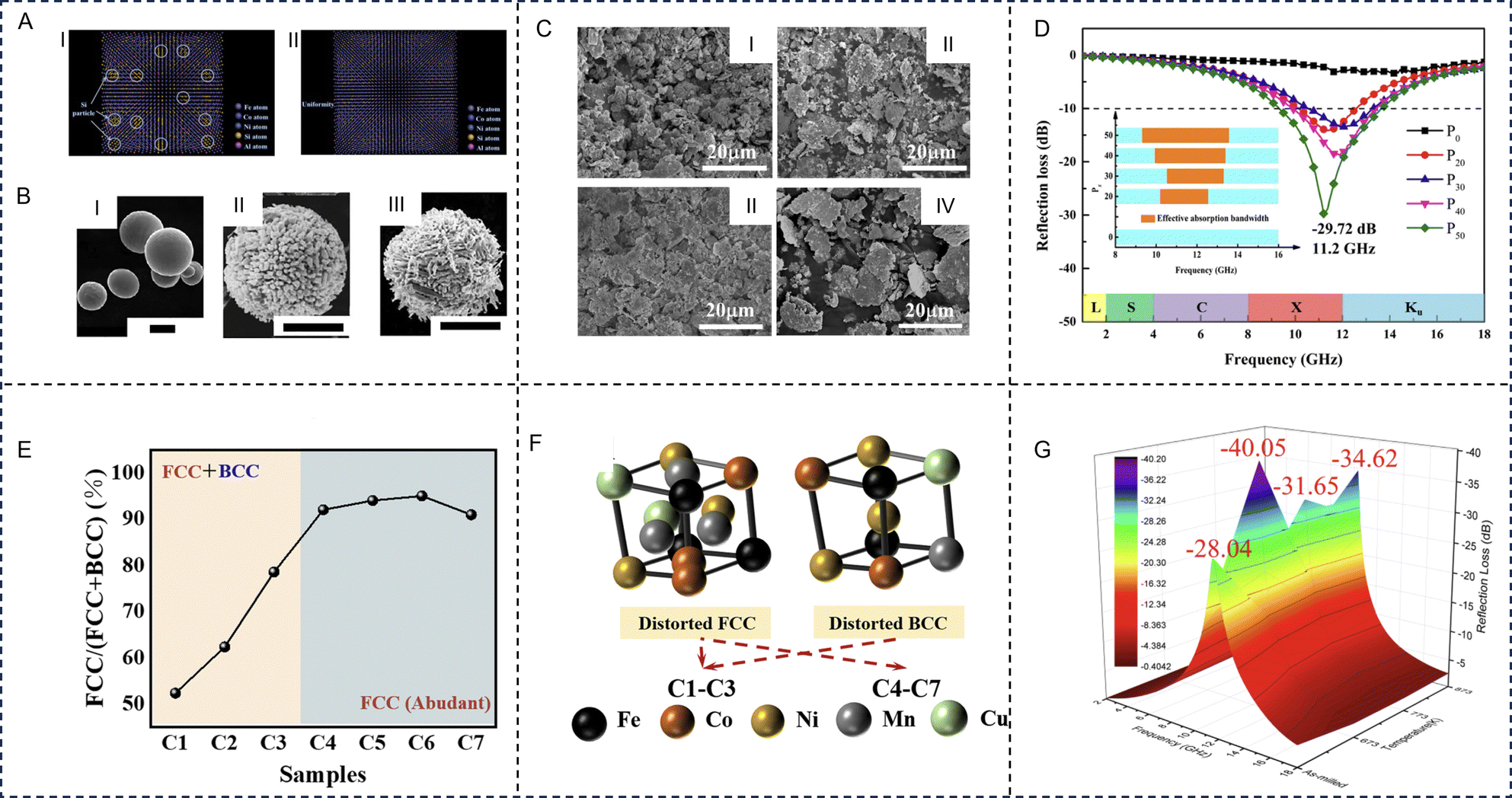 | ||
| Fig. 5 High-entropy alloys for electromagnetic wave absorption applications. The electromagnetic wave absorption properties of high-entropy alloys can be tailored accurately via control of uniformity: (A) Uniformity of FeCoNiSi0.4Al0.4 high-entropy alloy prepared through I: mechanical milling and II: melting-strip casting-milling. Reproduced with permission from ref. 112. Copyright (2018) Elsevier. Control of morphology: (B) scanning electron microscopy images of I: FeCoNiCrCuAl0.3 high-entropy alloy, II: FeCoNiCrCuAl0.3 high-entropy alloy under nitric acid treatment and III: FeCoNiCrCuAl0.3 HE alloy under nitric acid/cupric nitrate treatment. All the scales are 2 μm. Reproduced with permission from ref. 113. Copyright (2020) Elsevier. Control of structure: (C) scanning electron microscopy images of FeCoNiAlCr0.9 high-entropy alloy samples with different amounts of absolute ethanol, I: 0 ml, II: 20 ml, III: 30 ml, and IV: 40 ml, that was used as a process control agent. (D) Frequency dependence of microwave reflection loss with 2 mm thickness for the FeCoNiAlCr0.9 high-entropy alloy (Px, x = 0, 20, 30, 40 and 50) samples. Reproduced with permission from ref. 114. Copyright (2021) Elsevier. Control of element composition: (E) percentage of the fcc phase of FeCoNiCuxMn (x = 0, 0.1, 0.3, 0.5, 0.7, 0.9) high-entropy alloys (named C1, C2, C3, C4, C5, C6, respectively) and the C2 sample that was doped with a tiny amount of boron (FeCoNiCu0.1MnB0.05, named C7). (F) Phase structure of samples C1 to C7. Reproduced with permission from ref. 115. Copyright (2022) Royal Society of Chemistry (RSC). Control of the heat treatment process: (G) the reflection loss of the as-milled and annealed (at 673 K, 773 K and 873 K) FeCoNiCu0.5Al powders (d = 2 mm). Reproduced with permission from ref. 116. Copyright (2020) Elsevier. | ||
Different process parameters, such as ball milling speed, ball milling time, and the type or content of a process control agent, can lead to changes in the absorbing properties. Duan et al. studied the effect of the process control agent (anhydrous ethanol) content on EM wave absorption performance of FeCoNiAlCr0.9 HE alloys.114 When increasing the process control agent content from 0 to 50 ml, direct interaction between the alloy powder and the grinding ball is weakened, improving the aspect ratio and crystallinity of HE alloy powders (Fig. 5C). Concurrently, the lattice distortion, internal stress, and coercive force was reduced to regulate the magnetization saturation of the flake particles, which not only promoted the reflection loss but extended the effective bandwidth up to 4.28 GHz (Fig. 5D).
Additionally, the electromagnetic parameters of HE alloys can be improved by adjusting the element composition, thus affecting the electromagnetic absorbing properties. For example, metal elements such as Fe, Cu, and Ni, etc. can provide better magnetic loss characteristics, but can lead to impedance mismatches, resulting in a poorer electromagnetic loss ability. Therefore, the addition of other elements is necessary as it has been proven to drastically improve the loss ability. Duan et al. prepared flake shaped FeCoNiAlCrx alloys using mechanical alloying. The addition of Cr resulted in powder particles that were flatter and had more polarization sites, enhancing the surface polarization and ultimately increasing the real and imaginary parts of the complex permittivity (ε′ and ε′′).117 The real and imaginary parts of the complex permeability (μ′ and μ′′) decreased first and then increased as the proportion of Cr increased. The RLmin improved and settled into a low frequency region (from 11.20 GHz to 8.23 GHz) as the proportion of Cr increased, the EAB is increasing to 7.38 GHz. After annealing, the enhanced saturation magnetization (Ms) increased μr, and the crystallinity improved, increasing εr and indicating the positive effects of annealing treatment on reflection loss.
In multiphase HE alloys, each constituent phase has a significant role in the overall EM properties. It has been reported that the addition of elements, such as Ti, Mo, V, and Al, causes a noticeable effect on the phase separation in the studied alloys. For example, Cu modification strategies of some HE alloys can lead to phase change, which can induce excellent EM performances. Zhou et al. prepared FeCoNiCuxMn (x = 0, 0.1, 0.3, 0.5, 0.7 and 0.9) and FeCoNiCu0.1MnB0.05 HE alloys via an improved swing ball-milling method.115 With the introduction of Cu, sections of the bcc phase were transformed into the fcc phase, and the bcc phase almost completely disappeared for FeCoNiCu0.5Mn (Fig. 5E and F). Once synthesized, FeCoNiCu0.1Mn exhibited strong absorption of −71.0 dB while being as thin as 2.93 mm, with a broad bandwidth in the low-frequency range as wide as 6.79 GHz (7.75–14.54 GHz). The increase in EM performances may be attributed to plentiful polarization sites caused by Cu-introduced defects in HE alloys, and the enhanced magnetic loss may have potentially stemmed from high shape anisotropy. Further B doping was detrimental to corrosion resistance and EM wave absorption but enhanced the high temperature oxidation resistance.
Optimizing the heat treatment process is one of the most effective methods to improve the absorption performance of HE alloy materials. Under annealing conditions, the internal stress of HE alloy powder decreases, while the grain size and crystallinity increase, which is conducive to the improvement of magnetization saturation and absorption performance. Duan et al. studied the EM wave absorption performance of FeCoNiCu0.5Al at different annealing temperatures (673 K, 773 K, and 873 K).116 As the annealing temperature increased, the fcc phase in the alloy increased while the bcc phase decreased, until a single fcc phase is formed at the temperature of 773 K. After annealing, the internal stress of the alloy decreased and the particle size distribution was uniform, resulting in a new phase CoFe2O4 that increased the magnetic saturation and reduced reflection loss. At an annealing temperature of 773 K and a thickness of 2 mm, the RLmin of the alloy is −40.1 dB (Fig. 5G).
Recently, it has become difficult for a single HE alloy to achieve good impedance matching with free space. To further improve the absorption performance, the multi-component composite of HE alloy materials with other materials has become a research focal point. With the construction of multi-component composite materials, surface polarization can be increased, while achieving good impedance matching and improving the material's absorption performance. Chen et al. prepared porous HE alloy composite FeCoNiCrCuAl0.3@Air@La0.8Ca0.2CoO3 through hydrothermal and calcination methods. Assisted by the controlled design of composition and structures, the composite exhibited a strong magnetic loss ability and good impedance matching at medium/low frequencies at calcination temperatures of 350 °C and 450 °C.118 The dominated loss mechanisms included natural/exchange resonance, eddy current loss, and interfacial polarization. As the calcination temperature increases, the RLmin of the HE alloys changed significantly, with a RLmin of −38 dB at 350 °C, and a RLmin of −46 dB at 450 °C (thickness 3.7 mm, at the low-frequency point of 6.8 GHz).
We summarized the recent advancements in the major EM properties of HE alloys and HE alloy-based absorbers in Table 1. While the recent discoveries were able to lay groundwork for upcoming scientific discoveries, to obtain improved stabilities and tuneable EM wave absorption properties, low-dimensional nanostructured HE alloys should be developed based on quantitative, controllable reaction environments (liquid and gas phases) and driving forces (thermal and electrochemical reactions). Compared to the significant contribution of dielectric properties, the magnetic contribution of HE alloy has hardly been studied. Understanding and leveraging the effect of magnetic loss according to the low-dimensional nanostructure is also needed to clarify and boost the EM behaviours of HE alloys.
| Absorber | RLmin (dB) | EAB (GHz) | Thickness (mm) | Filler ratio (wt%) | Ref. |
|---|---|---|---|---|---|
| FeCoNiCuC0.37 | −61.1 | 8.0 | 1.95 | 70 | 119 |
| FeCoNiCuAl | −56 | 3.3 | 1.69 | 65 | 120 |
| FeCoNiCrAl | −45 | 4.3 | 1.5 | 70 | 14 |
| FeCoNiTi0.01Si | −68.4 | 5.2 | 1.69 | 70 | 121 |
| FeCoNiCrB0.05 | −62.5 | 5.8 | 2.03 | 70 | 122 |
| FeCoNiMnV0.5 | −57.4 | 6.2 | 2.24 | 80 | 123 |
| Fe10Co25Ni34Cu23Al8 | −39.4 | 6.6 | 1.9 | 80 | 124 |
| FeCoNiCrCu | −41.2 | 4.5 | 2.6 | 80 | 125 |
| FeCoNiCr0.6Mn | −66.9 | 4 | 2.8 | 70 | 126 |
| FeCoNiCu0.1Mn | −71 | 6.8 | 2.93 | 70 | 115 |
| FeCoNiMn0.5Al0.2 | −44.4 | 3.8 | 3 | 60 | 127 |
| FeCoCrAlGd0.1 | −45 | 5 | 1.5 | 70 | 128 |
| FeCoNiCuTi0.2 | −47.8 | 4.8 | 2.65 | 50 | 129 |
| FeCoNiCuC0.04 | −61.1 | 5.1 | 1.72 | 65 | 130 |
| Fe30Co30Ni30Si5Al5 | −47 | — | 2.3 | 37.5 | 131 |
| FeCoNiAlCr0.9 | −47.6 | — | 2.5 | 50 | 117 |
| FeCoNiMn0.5Al0.2 | −42.9 | — | 3 | 60 | 132 |
| FeCoNiCu0.5Al | −40.1 | — | 2 | 70 | 116 |
| FeCoNiCrCuAl0.3 | −40.2 | 4.5 | 1.7 | 50 | 113 |
| FeCoNi(Si0.6Al0.2B0.2) | −44.1 | 3.8 | 2 | 60 | 133 |
| FeCoNiCuAl | −19.2 | — | 2 | 60 | 134 |
| FeCoNiCrAl0.8 | −41.8 | 4.7 | 2.3 | 70 | 135 and 136 |
| FeCoNiCrAl | −35.3 | 2.7 | 1.5 | 70 | 16 |
| (FeCoNiSi8.9Al8.9)C0.2 | −43.6 | 13.5 | 2.8 | Metamaterial | 137 |
| (Fe28Co28Ni26Si8.9Al8.9)C0.2 | −50.9 | 12.1 | 1.9 | Metamaterial | 138 |
| CoNiFeCuV-C | −51.8 | 7.4 | 2.4 | 20 | 139 |
| L-CFP/FeCoNiCuZn-X | −82.6 | 3.2 | 1.55 | 30 | 140 |
| HCNF/FeCoNiCuMn | −65.8 | 7.7 | 3.5 | 2 | 141 |
| FeCoNiCuTi@C | −37.8 | 5.5 | 1.9 | 25 | 142 |
| Pt18Ni26Fe15Co14Cu27/rGO | −41.8 | 2.5 | 4 | 50 | 143 |
| FeCoNiTiMn@C | −33.4 | 5.5 | 1.9 | 50 | 144 |
| FeCoNiCrCuAl/PPy | −45.3 | 6.6 | 2.4 | 50 | 26 |
| FeCoNiCrCuAl0.3@air@La0.8Ca0.2CoO3 | −46.5 | 1.3 | 4.79 | 60 | 118 |
| FeCoNiCrCuAl0.3@air@Ni–NiO | −41.4 | 4 | 1.3 | 50 | 145 |
6.2. HE ceramics
HE ceramics are solid solutions of inorganic compounds with one or more Wyckoff sites shared by equal or near-equal atomic ratios of multi-principal elements, which mainly include HE oxides, carbides, and borides.146 The advent of HE ceramics provides more opportunities for overcoming the bottleneck for EM applications through synergistic dielectric/magnetic loss. Their diversity of band structure and chemical bonding broadens new avenues for composition design and property tuning. Generally, HE ceramics have been found to exhibit greater stability, enhanced mechanical properties, thermal and electrical conductivities, dielectric constant, and are promising in structural and functional EM wave absorption.147–149In perovskite oxides, substitution doping of A and B sites can cause severe lattice distortion, and the dual exchange effect of internal ions will jointly lead to the changes in electrical conductivity and magnetic properties. After manipulating entropy with hetero-valent ions, Jahn Teller distortion occurs inside the perovskite lattice increasing the structure symmetry, causing changes in the electric dipole moment to enhance dielectric loss. Zhao et al. prepared HE (Ca0.2Sr0.2Ba0.2La0.2Pb0.2)TiO3 by regulating the HE effect on perovskite components and achieved an effective absorption bandwidth (90% absorption) almost twice that of pure barium titanate.99 When compared with pure barium titanate, the HE perovskite material has a large number of interfaces and defects, which produce polarization effects when interacting with EM waves. Meanwhile, the pronounced lattice distortion induces high-density strain, creating multiple transport channels for electron carriers. Electron holography reveals that the HE (Ca0.2Sr0.2Ba0.2La0.2Pb0.2)TiO3 exhibits significant charge distribution around grain boundaries and strain-concentrated regions (Fig. 6A and B). The accumulation of positive and negative charges around numerous boundaries and strong strain location, is advantageous in enhancing dielectric polarization loss. The differential charge density maps between the oxygen and A-site atoms of several ceramic oxides are shown in Fig. 6C. As the HE effect gradually increases, the polarized region around the oxygen atom increases substantially, indicating the presence of considerable electron enrichment effects, most notably in the (Ca0.2Sr0.2Ba0.2La0.2Pb0.2)TiO3 sample. These effects are due to the presence of metal elements of differing valences within the oxide, forming abundant oxygen vacancies and leading to structural relaxation of the ions around the vacancies. When an oxygen atom is used to form an oxygen vacancy, electrons become abundantly bound around the A-site atom, resulting in electron enrichment. The abundance of local electrons in the metal atoms leads to stronger dipole polarization for EM wave loss (Fig. 6C).
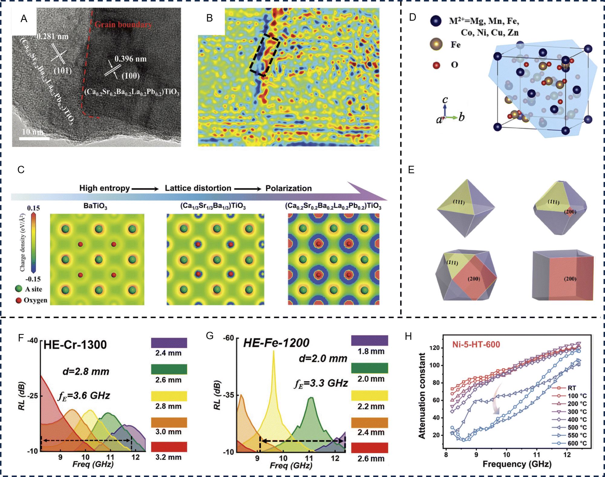 | ||
| Fig. 6 High-entropy oxides for electromagnetic wave absorption applications. BaTiO3-based high-entropy perovskites, (A) High-resolution transmission electron microscopy image and (B) reconstructed charge density distribution map of high-entropy (Ca0.2Sr0.2Ba0.2La0.2Pd0.2)TiO3, and (C) simulated charge density mappings of the three BaTiO3-based perovskites, suggesting the presence of considerable polarization with increasing entropy. Reproduced with permission from ref. 99. Copyright (2023) John Wiley and Sons. (D) Crystal structure with marked (111) plane and (E) computer-simulated morphologies of spinel ferrites grown with different growth rates on (111) and (200) faces viewed in the [100] direction. Reproduced with permission from ref. 150. Copyright (2022) Springer Nature. (F) Reflection loss values of high-entropy (Fe, Co, Ni, Cu, Mg)CrOx prepared at 1300 °C in the X-band with various thicknesses. (G) Reflection loss values of high-entropy (Fe, Co, Ni, Cu, Zn)Ox containing rock salt and spinel dual phases prepared at 1200 °C in the X-band with various thicknesses. Reproduced with permission from ref. 98. Copyright (2022) John Wiley and Sons. (H) The in situ measured attenuation constant of the high-temperature resistant nickel-based alloy within a high-entropy (FeCoNiCrMn)3O4 matrix. Reproduced with permission from ref. 151. Copyright (2023) John Wiley and Sons. | ||
As another example, spinel ferrite, with the general formula AB2O4, is one type of soft magnetic oxide that has high operating frequency and synergistic magnetic and dielectric loss capabilities. However, the generally poor impedance matching severely limits their EM applications. Entropy-increased spinel crystal structures can lead to the changes of magnetic and dielectric properties, thus directly influencing the absorption performance.
Zhao et al. designed three HE spinel ferrites, MFe2O4: (Mg0.2Mn0.2Fe0.2Co0.2Ni0.2)Fe2O4, (Mg0.2Fe0.2Co0.2Ni0.2Cu0.2)Fe2O4, and (Mg0.2Mn0.2Fe0.2Co0.2Zn0.2)Fe2O4, that all exhibit synergistic dielectric and magnetic loss.150Fig. 6D and E show the crystal structure and computer simulated equilibrium morphology of HE MFe2O4, which all present octahedral morphology with different orientations. In spinel, different stability energies of the crystal growth units affect the growth crystal face and stacking mode of growth units leading to different morphologies. The presence of HE magnetic components leads to the changes of morphologies, saturation magnetization and magneto-crystalline anisotropy, which contributes to the significant impact on effects of domain wall and natural resonance. While the enhancement of dielectric properties is attributed to the transition mechanism of nanodomains and resonance effects, (Mg0.2Mn0.2Fe0.2Co0.2Ni0.2)Fe2O4 demonstrates the best EM wave absorption performance, with a RLmin of −35.10 dB at 6.78 GHz; the EAB can reach 7.48 GHz (8.48 to 15.96 GHz), with a thickness of 2.4 mm.
Radoń et al. synthesized a novel (Zn, Mg, Ni, Fe, Cd)Fe2O4 HE spinel ferrite via the two-stage co-precipitation and annealing process.152 Lattice distortion and HE effects significantly increase the mobility of electrons, resulting in changes of conductivity and polarization process, and explain the superior microwave absorption performance in the low-frequency range of 1.9–2.1 GHz, with a reflection loss below −25 dB at the thickness of 0.8–1.0 cm.
Mohammadabadi et al. conducted a substitution of Co ions to change the magnetic content of HE spinel ferrite (MnNiCuZn)1−xCoxFe2O4 (x = 0.05, 0.10, 0.20, and 0.30).153 Its EM loss mainly comes from interface relaxation and ferromagnetic resonance. By increasing the Co content, the coercivity rises gradually while the saturation magnetization was slightly affected in the range of 67–71 emu g−1. The lowest reflection loss in the Ku band can reach −27 dB.
In order to further improve the EM wave loss performance and expand the application of HE ferrite materials, Zhao et al. prepared the biphasic spinel/perovskite HE oxide and achieved effective control of EM parameters through precise adjustment of crystal phase and structural defects.98 Significant stress concentration and lattice distortion were directly observed around the interface of the spinel (111)/perovskite (110) plane, leading to many point defects and stacking faults that are conducive to EM wave dissipation. Accordingly, the spinel/perovskite hybrid HE oxide (Fe, Co, Ni, Cu, Mg)CrOx prepared at 1300 °C and HE (Fe, Co, Ni, Cu, Zn)Ox containing rock salt and spinel dual phases prepared at 1200 °C exhibit excellent broadband microwave absorption in the X-band (Fig. 6F and G).
Aside from the tuneable EM wave absorption properties at room temperature, rational combined HE oxide composite can show apparent advantages in maintaining high temperature absorption performance. Dai et al. constructed an in situ conductive heterogeneous (FeCoNiCrMn)3O4 HE oxide-based composite, with the introduction of a conductive alloy phase after hydrogen treatment, the ohmic, dielectric polarization, and magnetic loss are enhanced synergistically, prompting the improvement of loss capacity and optimization of the impedance matching feature. The composites achieve over 90% absorption in the whole Ku band with a thickness of just 1.55 mm at room temperature and remain stable until reaching 500 °C (Fig. 6H).151
 | ||
Fig. 7 High-entropy carbides for electromagnetic wave absorption applications. (A) Electronic structure (left) and partial density of states (right), (B) low energy t2g (left) and high energy eg (right) levels of TiC, (C) comparison of reflection loss values of TMCs (TM = Ti, Zr, Hf, Nb, Ta), and (D) frequency dependence of reflection loss values of high-entropy (Ti0.2Zr0.2Hf0.2Nb0.2Ta0.2)C. Reproduced with permission from ref. 154. Copyright (2021) Elsevier. (E) Frequency-dependent real part and imaginary part of permittivity of (Ti0.2Zr0.2Hf0.2Nb0.2Ta0.2)C, (Ti0.2Zr0.2Mo0.2Nb0.2Ta0.2)C and (Ti0.2Zr0.2Cr0.2Nb0.2Ta0.2)C high-entropy carbides (HEC1, HEC2 and HEC3), and (F) schematic illustration of the electromagnetic wave absorption mechanisms. Reproduced with permission from ref. 155. Copyright (2023) Elsevier. (G) Schematic illustration of the electromagnetic wave absorption behaviours and mechanisms for the (Mo0.25Cr0.25Ti0.25V0.25)3AlC2 high-entropy MAX phase. Reproduced with permission from ref. 156. Copyright (2023) Elsevier. (H) Aberration corrected scanning transmission electron microscopy imaging and atomic lattice-resolved energy dispersive X-ray spectroscopy analysis of (Ti0.2V0.2Nb0.2Ta0.2Zr0.2)2FeC in the [1![[1 with combining macron]](https://www.rsc.org/images/entities/char_0031_0304.gif) 00] direction. The yellow, green, and gray balls represent atoms in the M-, A-, and X-sites, respectively. (I) Reflection loss curves of Nb2FeC, (Ti1/3Nb1/3Ta1/3)2FeC, and (Ti0.2V0.2Nb0.2Ta0.2Zr0.2)2FeC. Reproduced with permission from ref. 157. Copyright (2021) Springer Nature. 00] direction. The yellow, green, and gray balls represent atoms in the M-, A-, and X-sites, respectively. (I) Reflection loss curves of Nb2FeC, (Ti1/3Nb1/3Ta1/3)2FeC, and (Ti0.2V0.2Nb0.2Ta0.2Zr0.2)2FeC. Reproduced with permission from ref. 157. Copyright (2021) Springer Nature. | ||
Wang et al. prepared the HE transition metal carbides (Ti0.2Zr0.2Hf0.2Nb0.2Ta0.2)C, (Ti0.2Zr0.2Mo0.2Nb0.2Ta0.2)C and (Ti0.2Zr0.2Cr0.2Nb0.2Ta0.2)C, originating from the intrinsic conductivity of the HE carbides and lattice distortion resulting from a solid solution of multiple elements (Fig. 7E and F). The (Ti0.2Zr0.2Mo0.2Nb0.2Ta0.2)C with a 1.50 mm thickness displayed a minimal reflection loss of −32.1 dB, and the effective absorption bandwidth (<−10 dB) was in the frequency range of 13–18 GHz.155
MAX phase (where M stands for an early transition metal, A mostly denotes the group III or IV element, and X is either C or N) is a novel type of transition metal carbide material. Due to its covalent, ionic, and metallic bonding properties, it not only has good ductility, machinability, conductivity, but also possesses high-temperature oxidation resistance and stability, and is recognized as a promising absorbing material. Generally, the high conductivity of the MAX phase can cause strong reflection of EM waves, leading to a decrease in the absorption ability. By increasing the entropy of M-site atoms, the conductivity of the MAX phase can be reduced to an appropriate range, while the polarization ability can be enhanced, facilitating its microwave absorption performance. Qiao et al. successfully synthesized a novel HE (Mo0.25Cr0.25Ti0.25V0.25)3AlC2 MAX phase using a two-step solid-state reaction method, the synthesized HE MAX shows excellent EM wave absorption performance, with a RLmin of −45.80 dB at 1.7 mm and a maximum EAB of 3.6 GHz at 1.5 mm. After oxidation at 400–800 °C, Al2Mo3O12 and rutile phase titanium dioxide were formed, maintaining good EM wave absorption performance of the HE MAX phase within a certain frequency range (Fig. 7G).156
The HE components in HE MAX phases can change the conductivity, but also regulate their magnetic properties. Chen et al. used magnetic Fe atoms to in situ replace the A-site Al atoms in (Ti1/3Nb1/3Ta1/3)2AlC and (Ti0.2V0.2Nb0.2Ta0.2Zr0.2)2AlC MAX phases via isomorphic substitution reaction, successfully synthesizing a new MAX phase of (Ti1/3Nb1/3Ta1/3)2FeC and (Ti0.2V0.2Nb0.2Ta0.2Zr0.2)2FeC with ferromagnetic properties (Fig. 7H).157 With the increase in element composition of M-sites and Fe atomic layers in MAX phases, the EM wave absorption performance has been significantly improved, the RLmin value of (Ti0.2V0.2Nb0.2Ta0.2Zr0.2)2FeC reaches −42.7 dB at a thickness of 2 mm, and the effective bandwidth is 0.44 GHz (Fig. 7I).
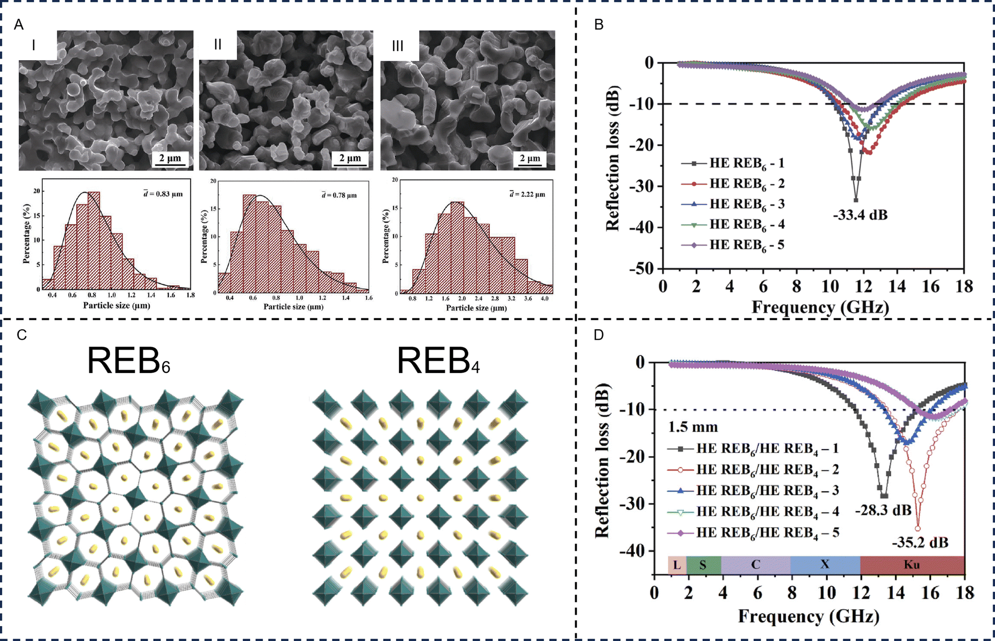 | ||
| Fig. 8 High-entropy borides for electromagnetic wave absorption applications. (A) Scanning electron microscope images and particle distributions of I: TMB2-1 (TM = Zr, Hf, Nb, Ta), II: high-entropy TMB2-2 (TM = Ti, Zr, Hf, Nb, Ta), and III: high-entropy TMB2-3 (TM = Cr, Zr, Hf, Nb, Ta), powders synthesized at 1950 °C for the dwelling time of 1 h. Reproduced with permission from ref. 158. Copyright (2023) John Wiley and Sons. (B) Comparison of reflection loss for HE REB6. Reproduced with permission from ref. 159. Copyright (2020) Springer Nature. (C) Crystal structure of REB6: RE atoms (yellow) and B6 octahedron (teal) are arranged in a CsCl-like packing. REB4: Altering sheets of RE atoms (yellow) and B6 octahedra (teal) linked by B2 units forming a quasi-layer structure. (D) Comparison of reflection loss of high-entropy REB6/high-entropy REB4. Reproduced with permission from ref. 160. Copyright (2021) Elsevier. | ||
Zhang et al. prepared five HE rare earth hexaboride using a one-step boron carbide reduction method.159 Among them, the (Ce0.2Y0.2Sm0.2Er0.2Yb0.2)B6 exhibits an average particle size of 1.86 μm and EM wave absorption performance with a RLmin of 11.5 GHz and a thickness of 2 mm, reaching −33.4 dB. Meanwhile, the optimized EAB reaches 3.9 GHz (13.6 GHz to 17.5 GHz) at a thickness of 1.5 mm (Fig. 8B).
By combing HE transition metal boride with HE composites, the dielectric loss ability can be effectively improved without sacrificing the magnetic loss ability, thereby achieving improved absorption performance. Zhang et al. synthesized five HE hexaboride/tetraboride (HE REB6/HE REB4) composite materials via combining hexaboride (HE REB6) with HE rare earth tetraboride (HE REB4) with high conductivity and strong magnetism (Fig. 8C and D).160 Among them, (Y0.2Nd0.2Sm0.2Eu0.2Er0.2)B6/(Y0.2Nd0.2Sm0.2Eu0.2Er0.2)B4 and (Y0.2Nd0.2Sm0.2Er0.2Yb0.2)B6/(Y0.2Nd0.2Sm0.2Er0.2Yb0.2)B4 HE composite materials show excellent absorption properties with a RLmin and EAB of −53.3 dB (1.7 mm), 4.2 GHz (1.5 mm), and −43.5 dB (1.3 mm), 4.2 GHz (1.5 mm), respectively. Table 2 shows the major EM performance of recently advanced HE ceramics and HE ceramics-based absorbers.
| Absorber | RLmin (dB) | EAB (GHz) | Thickness (mm) | Filler ratio (wt%) | Ref. |
|---|---|---|---|---|---|
| (FeCoNiCrMn)3O4 | −54.1 | 6.2 | 1.55 | 70 | 151 |
| (MgCoNiCuZn)O | −41.4 | 2.9 | 2 | — | 161 |
| (Ca0.2Sr0.2Ba0.2La0.2Pb0.2)TiO3 | −17.6 | 1.4 | 2 | 30 | 99 |
| (FeCoNiZn)xV2Oy | −36.5 | 2.8 | 2.2 | 100 | 162 |
| (Fe0.2Co0.2Ni0.2Cu0.2Mg0.2)Cr2O4/(Fe0.2Co0.2Ni0.2Cu0.2Mg0.2)CrO3 | −54.5 | 3.3 | 2 | — | 98 |
| (FeCo0.2Ni0.2Cr0.2Mn0.2)3O4 | −41.6 | 6 | 1.9 | 60 | 163 |
| (Mg0.2Mn0.2Fe0.2Co0.2Ni0.2)Fe2O4 | −35.1 | 7.5 | 2.4 | 70 | 150 |
| (Mg0.2Fe0.2Co0.2Ni0.2Cu0.2)Fe2O4 | −26.1 | 6.1 | 2.2 | 70 | 150 |
| (Mg0.2Fe0.2Co0.2Ni0.2Zn0.2)Fe2O4 | −27.4 | 6.5 | 2.2 | 70 | 150 |
| (Fe4CoNiCrMn)2O3 | −35 | 2.8 | 2.6 | 60 | 164 |
| (Zn,Mg,Ni,Fe,Cd)Fe2O4 | −18 | — | 1 | — | 152 |
| (MnNiCuZn)0.7Co0.3Fe2O4 | −27 | 2.5 | 5.3 | 70 | 153 |
| (MnNiCuZn)0.7Co0.3Fe2O4/graphene | −16 | 1.1 | 4.5 | 30 | 153 |
| (TaNbTiV)C | −48.8 | 4.8 | 1.8 | 50 | 165 |
| (Mo0.25Cr0.25Ti0.25V0.25)3C2Tx/FeCoNiCu | −50.8 | 3.8 | 1.61 | 65 | 166 |
| (V0.25Ti0.25Cr0.25Mo0.25)2GaC | −47.1 | 4.6 | 2.03 | 50 | 167 |
| (Hf0.25Zr0.25Nb0.25Ta0.25)C | −64.4 | 4.5 | 4.43 | 30 | 168 |
| (Mo0.25Cr0.25Ti0.25V0.25)3C2Tx | −45 | 5.6 | 1.65 | 35 | 169 |
| (Mo0.2Cr0.2Nb0.2Ti0.2V0.2)4C3Tx | −52.8 | 3.6 | 1.5 | 35 | 169 |
| (Zr0.2Ti0.2Hf0.2Nb0.2Ni0.2)C | −42.6 | 3.6 | 1 | 75 | 170 |
| (Zr0.2Ti0.2Hf0.2Ta0.2Cr0.2)C | −32.1 | 3 | 1.5 | 75 | 170 |
| (Zr0.2Ti0.2Hf0.2Nb0.2Cr0.2)C | −29.7 | 3.5 | 1.5 | 75 | 170 |
| (Zr0.2Ti0.2Hf0.2Ta0.2Cr0.2)C | −32.9 | 3.4 | 1.25 | 75 | 170 |
| (Ti1/5Zr1/5V1/5Nb1/5Ta1/5)2AlC | −47 | 3.9 | 2.78 | 70 | 171 |
| (Ti0.2Zr0.2Mo0.2Nb0.2Ta0.2)C | −32.1 | 5 | 1.5 | 96 | 155 |
| (Mo0.25Cr0.25Ti0.25V0.25)3AlC2 | −45.8 | 3.6 | 1.5 | 75 | 156 |
| (Ti0.2Zr0.2Hf0.2Nb0.2Ta0.2)C | −38.5 | 2.3 | 1.5 | — | 154 |
| (V0.6Ti0.2Cr0.2)2AlC | −56.2 | 4.2 | 2 | 30 | 172 |
| (Zr,Hf,Nb,Ta)C | −41.7 | 3.5 | 3 | 70 | 173 |
| (Cr,Zr,Hf,Nb,Ta)C | −21.6 | 10.5 | 2 | 70 | 173 |
| (Mo0.2Zr0.2Ti0.2Nb0.2Ta0.2)B2 | −36.4 | 1 | 6 | 30 | 174 |
| (Zr0.25Hf0.25Nb0.25Ta0.25)B2 | −59.6 | 7.6 | 2.3 | 70 | 158 |
| (Ti0.2Zr0.2Hf0.2Nb0.2Ta0.2)B2 | −47.2 | 3.6 | 2.7 | 70 | 158 |
| (Cr0.2Zr0.2Hf0.2Nb0.2Ta0.2)B2 | −56.2 | 11 | 2.2 | 70 | 158 |
| (Y0.2Nd0.2Sm0.2Eu0.2Er0.2)B6/(Y0.2Nd0.2Sm0.2Eu0.2Er0.2)B4 | −56.2 | 4.2 | 2 | 30 | 160 |
| (Y0.2Nd0.2Sm0.2 Er0.2Yb0.2)B6/(Y0.2Nd0.2Sm0.2Er0.2Yb0.2)B4 | −53.3 | 4.2 | 1.5 | 70 | 160 |
| (Ce0.2Y0.2Sm0.2Er0.2Yb0.2)B6 | −43.5 | 4.2 | 1.5 | 70 | 159 |
| (Ce0.2Y0.2Sm0.2Er0.2Yb0.2)B6/(Ce0.2Y0.2Sm0.2Er0.2Yb0.2)BO3 | −33.4 | 3.9 | 1.5 | 70 | 159 |
| (V,Ti,Ta,Nb)B2-SiC | −29.4 | 1.3 | 4 | 60 | 175 |
6.3. Other HE systems for EM wave absorption
In addition to the various HE alloys and HE ceramics mentioned above, novel entropy-stabilized systems including HE sulfides, HE metal halide perovskite and silicide/oxide hybrids have also been designed and tailored for EM applications.176–179When comparing with the oxygen atoms in HE oxides, the greater orbital extension and energetic match of the p orbitals in the sulfur atom with the d orbitals of the metals introduce additional space for tuning the reaction activity of atoms, which adjusts the probability of phase separation and helps effective EM wave absorption. The interfaces and configuration entropy of Cu-based sulfides can be modified by specific combinations of elements. Hui et al. proposed a novel multiphase interfacial engineering to eliminate the adverse impact of weak heterointerfaces on the EM wave absorption properties in HE sulfides. Stable HE Zn-based sulfides and phase-separated Cu-based sulfides were synthesized by a facile solvothermal approach. The results show that the high configuration entropy will result in a decrease in the charge density at Co atom sites and its weak electron exchange effect between Co/Ni and Fe atoms in HE Zn-based sulfides, leading to the lower EM parameters. As expected, the HE Zn-based sulfides (ZnFeCoNiCr-S) were failing to effectively absorb EM waves due to their limited heterointerface effects and low complex permittivity. In contrast, the multiphase Cu-based sulfides (CuFeCoNiCr-S) showed satisfactory EM wave absorption properties (i.e., EAB: 6.7 GHz at 2.00 mm) owing to the multiphase-induced interfacial polarization loss, caused by the specific interface of CuS (105)/CuFe2S3 (200). Furthermore, the single-phase ZnFeCoNiCr-S was transformed into a phase-separation structure through thermal decomposition at 400 °C. Due to the strong interfacial polarization induced by the FeNi2S4(311)/(Zn, Fe)S(111) phase interfaces, the EM wave absorption properties are significantly enhanced (EAB of 4.8 GHz at 1.45 mm). This study revealed the reasons for the limited EM wave absorption properties of HE sulfides and proposed multiphase interface engineering strategies to enhance interfacial charge accumulation and polarization.179 Hierarchical flower-like HE sulfides were also prepared via a simple solvothermal method and annealing process, where the dual-phase structure of the sulfide and local currents generated by sulfur vacancies induced both high interfacial polarization and conductivity loss to promote EM wave absorption.178
CsPbBr3 can undergo a transition between cubic, orthorhombic, and tetrahedral phases, among these the latter two phases show distortion in the lattice, beneficial for EM wave absorption.180,181 However, the limited stability and high lead content of CsPbBr3 hinder its bandwidth. Researchers propose leveraging the HE CsPbBr3 as a promising approach to tailor dielectric, electrical, and magnetic properties for EM wave absorption. Chen et al. reported excellent EM wave absorption properties for the Cs(Pb0.2Fe0.2Co0.2Ni0.2Mn0.2)3O3, including a RLmin of −75 dB at 10.2 GHz and a 2.5 mm thickness, accompanied by an exceptionally wide effective bandwidth of 8.8 GHz. In the HE perovskites, inherent mismatches in ion mass, size, and bonding state induce lattice distortions, generating structural defects conducive to EM wave loss.176
EM wave absorption materials composed of an electric insulating A phase and an electrical loss or magnetic loss B phase exhibit excellent EM wave absorption properties due to effective complementarities between the dielectric and magnetic loss.182 Rare earth oxides RE2O3 are electrically insulating. Rare earth silicide carbides RE3Si2C2 (RE = Y, La-Nd, Sm, Gd-Tm) show metallic conductivity and magnetic ordering temperatures lower than 60 K.183,184 HE rare earth silicides/oxides with good thermal stability, oxidation resistance, and low density are also expected to become a new type of EM wave absorption material. Chen et al. reported a series of novel HE rare earth silicide/rare earth oxide (RE3Si2C2/RE2O3) powders with efficient absorption bandwidth.177 Reasonable insulation HE RE2O3 provides higher dielectric loss and better impedance matching in the HE RE3Si2C2, which promotes more EM waves to reach the material. HE RE3Si2C2 with high carrier concentration will cause reflection and scattering between A and B phases in the material when interacting with EM waves, increasing the propagation path of EM waves. The heterogeneous interface between A and B phases can produce interface polarization and conductance loss effects under the action of EM waves. The optimal RLmin values and EAB of HE (Tm0.2Y0.2Pr0.2)Gd0.2Dy0.2)3Si2C2/HE (Tm0.2Y0.2Pr0.2Gd0.2Dy0.2)2O3 and HE (Tm0.2Y0.2Pr0.2Gd0.2Tb0.2)3Si2C2/HE (Tm0.2Y0.2Pr0.2Gd0.2Tb0.2)2O3) are −40.7 dB (2.9 mm), 3.4 GHz and −50.9 dB (2.0 mm), 4.5 GHz, respectively. Table 3 shows EM wave absorption performances of other HE systems and HE ceramics-based composite absorbers.
| Absorber | RLmin (dB) | EAB (GHz) | Thickness (mm) | Filler ratio (wt%) | Ref. |
|---|---|---|---|---|---|
| (Tm0.2Y0.2Dy0.2Gd0.2Tb0.2)3Si2C2 | −11.6 | 1.7 | 3.4 | — | 177 |
| (Tm0.2Y0.2Pr0.2Gd0.2Dy0.2)3Si2C2/(Tm0.2Y0.2Pr0.2Gd0.2Dy0.2)2O3) | −40.7 | 3.4 | 2.9 | — | 177 |
| (Tm0.2Y0.2Pr0.2Gd0.2Tb0.2)3Si2C2/(Tm0.2Y0.2Pr0.2Gd0.2Tb0.2)2O3) | −50.9 | 4.5 | 2 | — | 177 |
| CsMBr3(M = Pb, Fe, Co, Ni, Mn) | −75 | 8.8 | 2.5 | 70 | 176 |
| (FeCoNiCuZn)S | −45.8 | 3.8 | 1.4 | 50 | 178 |
| ZnFeCoNiCr-S | −17.3 | 4.8 | 1.45 | 50 | 179 |
7. Conclusions and perspectives
HE materials have shown a rapid growth in potential in EM wave absorption research due to their excellent synergistic properties. In this review, we summarized the fundamentals of EM wave absorption materials and the superiority of HE absorbers. We discussed advanced synthetic methods, in-depth characterization techniques, and electronic properties, especially with regard to regulatable electronic structures through band engineering of HE materials. Importantly, we focus on an overview of recent advancements in applying HE alloys, HE ceramics (mainly HE oxides, carbides, and borides) and other novel HE systems for EM wave absorption. As the prototype of HE materials, HE alloys combine the characteristics of site-occupancy disorder and lattice order to optimize the electronic structures of soft magnetic properties, thus exhibiting improved EM wave absorption performance compared with the corresponding low-element system. This performance is highly controllable and can be manipulated through various strategies such as optimizing the synthesis process, morphology, micro-structure, proportion of metal elements, and total amount of raw materials. Distinct from HE alloys, the diversity of defects (such as vacancies, interstitial atoms, lattice distortions, etc.) and electronic structures in HE ceramics allows for increased polarization centers, which suppress the dipole turning and space charge rearrangement under the high-frequency EM fields, leading to enhanced consumption of EM energy. Their dielectric and magnetic properties can be easily regulated, and the impedance matching and attenuation ability can also be controlled through manipulating the composition and lattice structures. Subsequently, HE materials may become the focal point of the field of EM functional materials. Despite these early achievements, it should be noted that the field of HE EM wave absorbers is still at its early stage where a vast number of challenges and opportunities coexist. To promote growth in research and applications, we propose the following perspectives.The EM wave absorption mechanism of HE materials is mainly based on enhanced dielectric and magnetic properties originating from the lattice distortion effect. To comprehend the fundamental science behind HE EM wave absorption materials, we need to explore qualitative explanations for lattice distortion mechanisms and conduct quantitative analyses of absorption mechanisms. To achieve this, the coalescence between theory and experimental evidence will be crucial. Until recently, the research on HE materials has remained mainly through “trial and error” approaches. We anticipate more studies on theoretical efforts that provide complementary insights into experimentation and enable accurate predictions. In the complex case of HE materials, the synergy between the multicomponent is difficult to explain with the conventional methods like density functional theory and kinetic models; by advancing reliable machine learning models and high-throughput calculation methods, we can develop a better understanding. It is also necessary to use extensive in situ high-frequency field characterization techniques such as spectral characterizations and visual characterizations based on STEM, to clarify and confirm real-time evolutions of HE magnetic and electric configurations under high-frequency EM fields.
With the rapid development of advanced synthesis and characterization techniques, progress, in terms of HE materials, is mainly focused toward the low-dimensional nanostructures. However, the disorder of microstructure in HE materials makes it difficult to control the free-standing synthesis when the target size is reduced to the sub-nanoscale. Due to the ultrasmall size, zero-dimensional sub-nanoscale HE materials would present more significant variations in the disordered atomic arrangement of high-utilization atoms. Additionally, unique properties are exhibited such as confinement and small size effect as well as the intrinsic major HE effects, allowing for customization of the charge distribution, electronic structure, magnetic moment, and band gap, etc. thus heavily altering the EM performance and a multitude of novel perspectives. Hence, building a deeper connection between the zero-dimensional structure and EM response properties is paramount for the future design of HE EM wave absorption materials, accelerating the development of related synthesis and characterization technology.
HE materials with unique high-temperature resistance (high strength and high plasticity at high temperatures) are expected to become the most valuable absorbers as they protect the long-term service of the heated component. However, most relative research on the HE EM wave absorption materials is tested at room temperature, while the high temperature EM properties have not been systemically reported. The breakthrough of high-temperature EM properties requires extensive and in-depth research on the evolution of microstructure, crystal phase, volume fraction, yield stress, etc. at elevated temperatures, requiring the development of reliable calculation methods and characterization in extreme high-temperature environments. Improving high-temperature performance through the control of components, microstructure, and interfacial interactions is an urgent challenge that is crucial for advancing the field.
Data availability
No primary research results, software or code have been included and no new data were generated or analysed as part of this review.Conflicts of interest
There are no conflicts to declare.Acknowledgements
X. Wang would like to acknowledge the financial support from the startup fund of The Ohio State University (OSU), OSU Sustainability Institute Seed Grant, OSU Materials Research Seed Grant Program, funded by the Center for Emergent Materials, an NSF-MRSEC, grant DMR-2011876, the Center for Exploration of Novel Complex Materials, and the Institute for Materials Research. H. Lv would like to acknowledge the financial support from the National Natural Science Foundation of China (no. 52301236) and the Shanghai Pujiang Program (no. 22PJ1401000).Notes and references
- A. Iqbal, F. Shahzad, K. Hantanasirisakul, M. K. Kim, J. Kwon, J. Hong, H. Kim, D. Kim, Y. Gogotsi and C. M. Koo, Science, 2020, 369, 446–450 CrossRef CAS PubMed.
- D. Lan, Y. Hu, M. Wang, Y. Wang, Z. Gao and Z. Jia, Compos. Commun., 2024, 50, 101993 CrossRef.
- H. Lv, Y. Yao, M. Yuan, G. Chen, Y. Wang, L. Rao, S. Li, U. I. Kara, R. L. Dupont, C. Zhang, B. Chen, B. Liu, X. Zhou, R. Wu, S. Adera, R. Che, X. Zhang and X. Wang, Nat. Commun., 2024, 15, 1295 CrossRef CAS PubMed.
- H. Lv, Z. Yang, H. Pan and R. Wu, Prog. Mater. Sci., 2022, 127, 100946 CrossRef CAS.
- H. Lv, Z. Yang, H. Xu, L. Wang and R. Wu, Adv. Funct. Mater., 2019, 30, 1907251 CrossRef.
- Z. Lou, Q. Wang, X. Zhou, U. I. Kara, R. S. Mamtani, H. Lv, M. Zhang, Z. Yang, Y. Li, C. Wang, S. Adera and X. Wang, J. Mater. Sci. Technol., 2022, 113, 33–39 CrossRef CAS.
- H. Lv, Y. Yao, S. Li, G. Wu, B. Zhao, X. Zhou, R. L. Dupont, U. I. Kara, Y. Zhou, S. Xi, B. Liu, R. Che, J. Zhang, H. Xu, S. Adera, R. Wu and X. Wang, Nat. Commun., 2023, 14, 1982 CrossRef CAS PubMed.
- M. Liu, Z. Wang, Z. Song, F. Wang, G. Zhao, H. Zhu, Z. Jia, Z. Guo, F. Kang and C. Yang, Nat. Commun., 2024, 15, 5486 CrossRef CAS PubMed.
- Y. Cheng, X. Li, Y. Qin, Y. Fang, G. Liu, Z. Wang, J. Matz, P. Dong, J. Shen and M. Ye, Sci. Adv., 2021, 7, eabj1663 CrossRef CAS PubMed.
- L. Wang, M. Huang, X. Yu, W. You, J. Zhang, X. Liu, M. Wang and R. Che, Nano-Micro Lett., 2020, 12, 150 CrossRef CAS.
- Y. Q. Wang, M. Cao, B. W. Liu, F. R. Zeng, Q. Fu, H. B. Zhao and Y. Z. Wang, Mater. Horiz., 2024, 11, 978–987 RSC.
- H. Lv, Z. Yang, B. Liu, G. Wu, Z. Lou, B. Fei and R. Wu, Nat. Commun., 2021, 12, 834 CrossRef CAS.
- X. Zeng, T. Nie, C. Zhao, Y. Gao and X. Liu, Adv. Sci., 2024, 11, 2403723 CrossRef CAS.
- T. Wang, Y. Zhang, G. Bai and X. Liu, J. Mater. Res., 2023, 39, 248–261 CrossRef.
- S. Zhang, D. Lan, J. Zheng, Z. Zhao, Z. Jia and G. Wu, Cell Rep. Phys. Sci., 2024, 5, 102206 CrossRef.
- P. Yang, Y. Liu, X. Zhao, J. Cheng and H. Li, Adv. Powder Technol., 2016, 27, 1128–1133 CAS.
- C. Sun, D. Lan, Z. Jia, Z. Gao and G. Wu, Small, 2024, 2405874 CAS.
- Z. Lou, Q. Wang, U. I. Kara, R. S. Mamtani, X. Zhou, H. Bian, Z. Yang, Y. Li, H. Lv, S. Adera and X. Wang, Nano-micro Lett., 2021, 14, 11 Search PubMed.
- C. He, Y. Li, Z. H. Zhou, B. H. Liu and X. H. Gao, Adv. Mater., 2024, 36, 2400920 CrossRef CAS.
- Y. Xia, W. Gao and C. Gao, Adv. Funct. Mater., 2022, 32, 2204591 CrossRef CAS.
- X. Huang, G. Yu, Y. Zhang, M. Zhang and G. Shao, Chem. Eng. J., 2021, 426, 131894 CrossRef CAS.
- Z. Wu, H. W. Cheng, C. Jin, B. Yang, C. Xu, K. Pei, H. Zhang, Z. Yang and R. Che, Adv. Mater., 2022, 34, 2107538 CrossRef CAS.
- G. Chen, R. Zhang, M. Yuan, S. Xue, Y. Liu, B. Li, K. Luo, Y. Lai, J. Zhang, H. Lv and R. Che, Adv. Mater., 2024, 36, 2313411 CrossRef CAS.
- M. Yuan, H. Lv, H. Cheng, B. Zhao, G. Chen, J. Zhang and R. Che, Adv. Funct. Mater., 2023, 2302003 CrossRef CAS.
- X. Lv, H. Lv, Y. Huang, R. Zhang, G. Qin, Y. Dong, M. Liu, K. Pei, G. Cao, J. Zhang, Y. Lai and R. Che, Nat. Commun., 2024, 15, 3278 CrossRef CAS.
- L. Zhang, J. Jia, H. Liang and G. Chen, J. Mater. Sci.: Mater. Electron., 2021, 32, 26074–26085 CrossRef CAS.
- Z. Wang, H. Bi, P. Wang, M. Wang, Z. Liu, L. Shen and X. Liu, Phys. Chem. Chem. Phys., 2015, 17, 3796–3801 RSC.
- G. He, Y. Duan and H. Pang, Nano-Micro Lett., 2020, 12, 57 CrossRef CAS.
- J. M. Schins, P. Prins, F. C. Grozema, R. D. Abellón, M. P. de Haas and L. D. A. Siebbeles, Rev. Sci. Instrum., 2005, 76, 084703 CrossRef.
- Y. Liu, Z. Jia, Q. Zhan, Y. Dong, Q. Xu and G. Wu, Nano Res., 2022, 15, 5590–5600 CrossRef CAS.
- H. Zhang, X. Zhou, M. Yuan, Y. Du, X. Xiong, X. Lv, Y. Liu, H. Lv, Y. Lai, D. Pan and R. Che, Adv. Funct. Mater., 2024, 2406137 CrossRef.
- X. Zhou, H. Zhang, M. Yuan, B. Li, J. Cui, Y. Qian, Y. Liu, L. Yu, X. Xiong, Y. Du, J. Zhang, Y. Lai, H. Lv and R. Che, Adv. Funct. Mater., 2024, 2314541 CrossRef.
- J. Azadmanjiri, J. Wang, C. C. Berndt, A. Kapoor, D. M. Zhu, A. S. M. Ang and V. K. Srivastava, Ind. Eng. Chem. Res., 2017, 56, 434–439 CrossRef CAS.
- C. Sun, Z. Jia, S. Xu, D. Hu, C. Zhang and G. Wu, J. Mater. Sci. Technol., 2022, 113, 128–137 CrossRef CAS.
- Q. Liu, Q. Cao, H. Bi, C. Liang, K. Yuan, W. She, Y. Yang and R. Che, Adv. Mater., 2015, 28, 486–490 CrossRef PubMed.
- H. Qi, L. Chen, S. Deng and J. Chen, Nat. Rev. Mater., 2023, 8, 355–356 CrossRef CAS.
- C. Oses, C. Toher and S. Curtarolo, Nat. Rev. Mater., 2020, 5, 295–309 CrossRef CAS.
- E. P. George, D. Raabe and R. O. Ritchie, Nat. Rev. Mater., 2019, 4, 515–534 CrossRef CAS.
- B. Ouyang and Y. Zeng, Nat. Commun., 2024, 15, 973 CrossRef CAS.
- Y. Yao, Q. Dong, A. Brozena, J. Luo, J. Miao, M. Chi, C. Wang, I. G. Kevrekidis, Z. J. Ren, J. Greeley, G. Wang, A. Anapolsky and L. Hu, Science, 2022, 376, 151 CrossRef.
- S. Wei, S. J. Kim, J. Kang, Y. Zhang, Y. Zhang, T. Furuhara, E. S. Park and C. C. Tasan, Nat. Mater., 2020, 19, 1175–1181 CrossRef CAS.
- S. Divilov, H. Eckert, D. Hicks, C. Oses, C. Toher, R. Friedrich, M. Esters, M. J. Mehl, A. C. Zettel, Y. Lederer, E. Zurek, J. P. Maria, D. W. Brenner, X. Campilongo, S. Filipovic, W. G. Fahrenholtz, C. J. Ryan, C. M. DeSalle, R. J. Crealese, D. E. Wolfe, A. Calzolari and S. Curtarolo, Nature, 2024, 625, 66–73 CrossRef CAS PubMed.
- B. Yang, Y. Zhang, H. Pan, W. Si, Q. Zhang, Z. Shen, Y. Yu, S. Lan, F. Meng, Y. Liu, H. Huang, J. He, L. Gu, S. Zhang, L. Q. Chen, J. Zhu, C. W. Nan and Y. H. Lin, Nat. Mater., 2022, 21, 1074–1080 CrossRef CAS.
- Y. Zeng, B. Ouyang, J. Liu, Y. W. Byeon, Z. Cai, L. J. Miara, Y. Wang and G. Ceder, Science, 2022, 378, 1320–1324 CrossRef CAS.
- S. Moniri, Y. Yang, J. Ding, Y. Yuan, J. Zhou, L. Yang, F. Zhu, Y. Liao, Y. Yao, L. Hu, P. Ercius and J. Miao, Nature, 2023, 624, 564–569 CrossRef CAS.
- S. C. Kim, J. Wang, R. Xu, P. Zhang, Y. Chen, Z. Huang, Y. Yang, Z. Yu, S. T. Oyakhire, W. Zhang, L. C. Greenburg, M. S. Kim, D. T. Boyle, P. Sayavong, Y. Ye, J. Qin, Z. Bao and Y. Cui, Nat. Energy, 2023, 8, 814–826 CrossRef CAS.
- M. Yuan, B. Zhao, C. Yang, K. Pei, L. Wang, R. Zhang, W. You, X. Liu, X. Zhang and R. Che, Adv. Funct. Mater., 2022, 32, 2203161 CrossRef CAS.
- H. Lv, X. Zhou, G. Wu, U. I. Kara and X. Wang, J. Mater. Chem. A, 2021, 9, 19710–19718 RSC.
- C. Yang, Y. Huang, K. Pei, X. Long, L. Yang, Y. Luo, Y. Lai, J. Zhang, G. Cao and R. Che, Adv. Mater., 2024, 36, 2311831 CrossRef CAS.
- P. Liu, Y. Li, H. Xu, L. Shi, J. Kong, X. Lv, J. Zhang and R. Che, ACS Nano, 2024, 18, 560–570 CrossRef CAS PubMed.
- X. Lv, K. Pei, C. Yang, G. Qin, M. Liu, J. Zhang and R. Che, ACS Nano, 2022, 16, 19319–19327 CrossRef CAS PubMed.
- H. Lv, J. Cui, B. Li, M. Yuan, J. Liu and R. Che, Adv. Funct. Mater., 2024, 2315722 CrossRef.
- Y. Yao, Z. Huang, P. Xie, S. D. Lacey, R. J. Jacob, H. Xie, F. Chen, A. N. Nie, T. Pu, M. Rehwoldt, D. Yu, M. R. Zachariah, C. Wang, R. Shahbazian-Yassar, J. Li and L. Hu, Science, 2018, 359, 1489–1494 CrossRef CAS.
- S. Gao, S. Hao, Z. Huang, Y. Yuan, S. Han, L. Lei, X. Zhang, R. Shahbazian-Yassar and J. Lu, Nat. Commun., 2020, 11, 2016 CrossRef CAS.
- M. Cui, C. Yang, B. Li, Q. Dong, M. Wu, S. Hwang, H. Xie, X. Wang, G. Wang and L. Hu, Adv. Energy Mater., 2020, 11, 2002887 CrossRef.
- M. Liu, Z. Zhang, F. Okejiri, S. Yang, S. Zhou and S. Dai, Adv. Mater. Interfaces, 2019, 6, 1900015 CrossRef CAS.
- M. W. Glasscott, A. D. Pendergast, S. Goines, A. R. Bishop, A. T. Hoang, C. Renault and J. E. Dick, Nat. Commun., 2019, 10, 2650 CrossRef PubMed.
- B. Wang, C. Wang, X. W. Yu, Y. Cao, L. F. Gao, C. P. Wu, Y. F. Yao, Z. Q. Lin and Z. G. Zou, Nat. Synth., 2022, 1, 138 CrossRef.
- P. Padhy, M. A. Zaman, M. A. Jensen, Y. T. Cheng, Y. Huang, M. Wu, L. Galambos, R. W. Davis and L. Hesselink, Nat. Commun., 2024, 15, 6159 CrossRef CAS.
- J. Gild, Y. Zhang, T. Harrington, S. Jiang, T. Hu, M. C. Quinn, W. M. Mellor, N. Zhou, K. Vecchio and J. Luo, Sci. Rep., 2016, 6, 37946 CrossRef CAS.
- S. K. Wu, Y. Pan, N. Wang, T. Lu and W. J. Dai, Int. J. Miner., Metall. Mater., 2019, 26, 124–132 CAS.
- Z. Y. Lv, X. J. Liu, B. Jia, H. Wang, Y. Wu and Z. P. Lu, Sci. Rep., 2016, 6, 34213 CAS.
- J. Cao and S. Tao, Nat. Commun., 2024, 15, 5579 CAS.
- R. Dong, R. Liu, P. R. J. Gaffney, M. Schaepertoens, P. Marchetti, C. M. Williams, R. Chen and A. G. Livingston, Nat. Chem., 2019, 11, 136–145 CrossRef CAS PubMed.
- D. Wang, Z. Liu, S. Du, Y. Zhang, H. Li, Z. Xiao, W. Chen, R. Chen, Y. Wang, Y. Zou and S. Wang, J. Mater. Chem. A, 2019, 7, 24211–24216 RSC.
- D. Lai, Q. Kang, F. Gao and Q. Lu, J. Mater. Chem. A, 2021, 9, 17913–17922 RSC.
- L. Spiridigliozzi, C. Ferone, R. Cioffi and G. Dell’Agli, Acta Mater., 2021, 202, 181–189 CrossRef CAS.
- D. Wu, K. Kusada, T. Yamamoto, T. Toriyama, S. Matsumura, I. Gueye, O. Seo, J. Kim, S. Hiroi, O. Sakata, S. Kawaguchi, Y. Kubota and H. Kitagawa, Chem. Sci., 2020, 11, 12731–12736 RSC.
- G. Feng, F. Ning, J. Song, H. Shang, K. Zhang, Z. Ding, P. Gao, W. Chu and D. Xia, J. Am. Chem. Soc., 2021, 143, 17117–17127 CrossRef CAS PubMed.
- C. R. McCormick and R. E. Schaak, J. Am. Chem. Soc., 2021, 143, 1017–1023 CrossRef CAS.
- B. Ward-O’Brien, E. J. Pickering, R. Ahumada-Lazo, C. Smith, X. L. Zhong, Y. Aboura, F. Alam, D. J. Binks, T. L. Burnett and D. J. Lewis, J. Am. Chem. Soc., 2021, 143, 21560–21566 CrossRef.
- M. Azad Malik, M. Afzaal and P. O’Brien, Chem. Rev., 2010, 110, 4417–4446 CrossRef PubMed.
- J. Qu, A. Elgendy, R. Cai, M. A. Buckingham, A. A. Papaderakis, H. de Latour, K. Hazeldine, G. F. S. Whitehead, F. Alam, C. T. Smith, D. J. Binks, A. Walton, J. M. Skelton, R. A. W. Dryfe, S. J. Haigh and D. J. Lewis, Adv. Sci., 2023, 10, 2204488 CrossRef CAS PubMed.
- D. Lai, L. Ling, M. Su, Q. Kang, F. Gao and Q. Lu, Chem. Sci., 2023, 14, 1787–1796 RSC.
- X. Xu, Z. Shao and S. P. Jiang, Energy Technol., 2022, 10, 2200573 CrossRef CAS.
- G. Fang, J. Gao, J. Lv, H. Jia, H. Li, W. Liu, G. Xie, Z. Chen, Y. Huang, Q. Yuan, X. Liu, X. Lin, S. Sun and H. J. Qiu, Appl. Catal., B, 2020, 268, 118431 CrossRef CAS.
- H. J. Qiu, G. Fang, Y. Wen, P. Liu, G. Xie, X. Liu and S. Sun, J. Mater. Chem. A, 2019, 7, 6499–6506 RSC.
- Z. Jin, J. Lv, H. Jia, W. Liu, H. Li, Z. Chen, X. Lin, G. Xie, X. Liu, S. Sun and H. J. Qiu, Small, 2019, 15, 1904180 CrossRef CAS.
- Z. Jin, J. Lyu, Y. L. Zhao, H. Li, Z. Chen, X. Lin, G. Xie, X. Liu, J. J. Kai and H. J. Qiu, Chem. Mater., 2021, 33, 1771–1780 CrossRef CAS.
- Q. Ding, Y. Zhang, X. Chen, X. Fu, D. Chen, S. Chen, L. Gu, F. Wei, H. Bei, Y. Gao, M. Wen, J. Li, Z. Zhang, T. Zhu, R. O. Ritchie and Q. Yu, Nature, 2019, 574, 223–227 CrossRef CAS PubMed.
- S. V. G. Ayyagari, L. Miao, M. Webb, J. Heron and N. Alem, Microsc. Microanal., 2023, 29, 1768–1769 Search PubMed.
- Y. Wen and Y. Liu, Ceram. Int., 2023, 49, 26141–26146 CAS.
- J. He, M. Song, M. Yang and M. Zhu, J. Am. Ceram. Soc., 2023, 107, 615–623 CrossRef.
- P. R. Jothi, W. Liyanage, B. Jiang, S. Paladugu, D. Olds, D. A. Gilbert and K. Page, Small, 2021, 18, 2101323 Search PubMed.
- J. Liu, Y. Li, Z. Chen, N. Liu, L. Zheng, W. Shi and X. Wang, J. Am. Chem. Soc., 2022, 144, 23191–23197 CrossRef CAS PubMed.
- Z. Jia, T. Yang, L. Sun, Y. Zhao, W. Li, J. Luan, F. Lyu, L. C. Zhang, J. J. Kruzic, J. J. Kai, J. C. Huang, J. Lu and C. T. Liu, Adv. Mater., 2020, 32, 2000385 CrossRef CAS PubMed.
- A. Naughton-Duszová, P. Švec, A. Kovalčíková, R. Sedlák, P. Tatarko, P. Hvizdoš, P. Šajgalík and J. Dusza, J. Eur. Ceram., 2023, 43, 6765–6773 CrossRef.
- E. A. Anber, D. Beaudry, C. Brandenburg, S. Lech, L. Backman, D. L. Foley, E. L. Wang, M. J. Waters, L. Perriere, J. P. Couzinie, J. M. Rondinelli, E. Opila and M. L. Taheri, Scr. Mater., 2024, 244, 115997 CrossRef CAS.
- Y. T. Yeh, C. W. Huang, A. Y. Hou, C. Y. Huang, Y. D. Lin and W. W. Wu, Small, 2024, 20, 2307284 CrossRef CAS.
- X. Ke, M. Zhang, K. Zhao and D. Su, Small Methods, 2021, 6, 2101040 CrossRef PubMed.
- F. Brenne, A. S. K. Mohammed and H. Sehitoglu, Ultramicroscopy, 2020, 219, 113134 CrossRef CAS.
- J. Zhu, Z. Li, S. T. Yang, Y. R. Zhao, F. C. Lang and Y. M. Xing, Opt. Lasers Eng., 2023, 163, 107457 CrossRef.
- W. Chang and T. D. Brown, Micron, 2011, 42, 392–400 CrossRef CAS.
- I. Alam, M. A. Adaan-Nyiak, S. Hwang, K. Kisslinger, M. Topsakal, E. Jossou, S. K. Gill and A. A. Tiamiyu, Mater. Charact., 2024, 209, 113722 CrossRef CAS.
- M. Jafary-Zadeh, K. H. Khoo, R. Laskowski, P. S. Branicio and A. V. Shapeev, J. Alloys Compd., 2019, 803, 1054–1062 CrossRef CAS.
- Y. Y. Tan, M. Y. Su, Z. C. Xie, Z. J. Chen, Y. Gong, L. R. Zheng, Z. Shi, G. Mo, Y. Li, L. W. Li, H. Y. Wang and L. H. Dai, Intermetallics, 2021, 129, 107050 CAS.
- B. Schuh, F. Mendez-Martin, B. Völker, E. P. George, H. Clemens, R. Pippan and A. Hohenwarter, Acta Mater., 2015, 96, 258–268 CAS.
- B. Zhao, Y. Du, Z. Yan, L. Rao, G. Chen, M. Yuan, L. Yang, J. Zhang and R. Che, Adv. Funct. Mater., 2022, 33, 2209924 Search PubMed.
- B. Zhao, Z. Yan, Y. Du, L. Rao, G. Chen, Y. Wu, L. Yang, J. Zhang, L. Wu, D. W. Zhang and R. Che, Adv. Mater., 2023, 35, 2210243 CAS.
- X. Sun, C. Xu, P. Ji, Z. Tang, S. Jiao, Y. Lu, M. Zhao, H. L. Cai and X. S. Wu, Ceram. Int., 2023, 49, 17091–17098 CrossRef CAS.
- A. L. F. Cardoso, C. P. F. Perdomo, B. G. Foschiani, I. C. S. Barbara, J. A. Xaraba, F. L. Zabotto and R. F. K. Gunnewiek, Mater. Lett., 2023, 333, 133539 CrossRef CAS.
- Y. Wang, B. Yu, M. He, Z. Zhai, K. Yin, F. Kong and Z. Zhang, Nano Res., 2021, 15, 4820–4826 CrossRef.
- H. Li, M. Sun, Y. Pan, J. Xiong, H. Du, Y. Yu, S. Feng, Z. Li, J. Lai, B. Huang and L. Wang, Appl. Catal., B, 2022, 312, 121431 CrossRef CAS.
- R. Wang, M. Chen, J. Han, X. Zhang, Z. Zhang, T. Yao, Y. Wang, L. Xu, X. Wang, P. Xu and B. Song, Adv. Funct. Mater., 2023, 34, 2312322 CrossRef.
- N. J. Usharani, P. Arivazhagan, T. Thomas and S. S. Bhattacharya, Mater. Sci. Eng., B, 2022, 283, 115847 CrossRef CAS.
- Y. Mizuguchi, H. Usui, R. Kurita, K. Takae, M. R. Kasem, R. Matsumoto, K. Yamane, Y. Takano, Y. Nakahira, A. Yamashita, Y. Goto, A. Miura and C. Moriyoshi, Mater. Today Phys., 2023, 32, 101019 CrossRef CAS.
- N. J. Usharani, H. Sanghavi and S. S. Bhattacharya, J. Alloys Compd., 2021, 888, 161390 CrossRef CAS.
- R. He, L. Yang, Y. Zhang, D. Jiang, S. Lee, S. Horta, Z. Liang, X. Lu, A. Ostovari Moghaddam, J. Li, M. Ibáñez, Y. Xu, Y. Zhou and A. Cabot, Adv. Mater., 2023, 35, 2303719 CrossRef CAS.
- R. R. Katzbaer, F. M. dos Santos Vieira, I. Dabo, Z. Mao and R. E. Schaak, J. Am. Chem. Soc., 2023, 145, 6753–6761 CrossRef CAS PubMed.
- J. Mayandi, T. G. Finstad, Ø. Dahl, P. Vajeeston, M. Schrade, O. M. Løvvik, S. Diplas and P. A. Carvalho, Thin Solid Films, 2022, 744, 139083 CrossRef CAS.
- K. Gan, C. Cai, C. Zong, D. Duan and J. Yang, Ceram. Int., 2022, 48, 23963–23974 CrossRef CAS.
- B. Zhang, Y. Duan, Y. Cui, G. Ma, T. Wang and X. Dong, Mater. Design, 2018, 149, 173–183 CrossRef CAS.
- D. Lan, Z. Zhao, Z. Gao, K. Kou, G. Wu and H. Wu, J. Magn. Magn. Mater., 2020, 512, 167065 CrossRef CAS.
- Y. Duan, H. Pang, X. Wen, X. Zhang and T. Wang, J. Mater. Sci. Technol., 2021, 77, 209–216 CrossRef CAS.
- H. Zhou, L. Jiang, L. Jia, Z. Tang, L. Wang, A. Wu and X. Zhang, J. Mater. Chem. C, 2022, 10, 16696–16705 RSC.
- Y. Duan, L. Song, Y. Cui, H. Pang, X. Zhang and T. Wang, J. Alloys Compd., 2020, 848, 156491 CrossRef CAS.
- Y. Duan, X. Wen, B. Zhang, G. Ma and T. Wang, J. Magn. Magn. Mater., 2020, 497, 165947 CrossRef CAS.
- G. Chen, H. Yin, B. Luo and L. Zhang, J. Mater. Sci.: Mater. Electron., 2020, 31, 6435–6448 CrossRef CAS.
- Z. Qiu, X. Liu, T. Yang, J. Wang, Y. Wang, W. Ma and Y. Huang, Adv. Funct. Mater., 2024, 2400220 CrossRef CAS.
- L. Jia, L. Jiang, J. Yang, J. Liu, A. Wu and X. Zhang, Appl. Phys. Lett., 2024, 124, 092404 CrossRef CAS.
- L. Jia, L. Jiang, H. Zhou, S. Yan, A. Wu and X. Zhang, Phys. Chem. Chem. Phys., 2023, 25, 22011–22021 RSC.
- H. Zhou, L. Jiang, L. Jia, S. Zhu, L. Wang, A. Wu and X. Zhang, J. Alloys Compd., 2023, 959, 170579 CrossRef CAS.
- H. Zhou, L. Jiang, S. Zhu, L. Jia, A. Wu and X. Zhang, J. Alloys Compd., 2023, 946, 169402 CrossRef CAS.
- L. Liang, J. Wu, Z. Yin, C. Kong, A. Pervikov, H. Shi, X. Li and A. Qiu, Appl. Phys. Lett., 2024, 124, 053502 CrossRef CAS.
- G. Li, H. Zhao, H. Wang, Z. Zhou, L. Gao, W. Su and C. Dong, J. Alloys Compd., 2023, 941, 168822 CrossRef CAS.
- H. Zhou, L. Jiang, S. Zhu, L. Wang, Y. Hu, X. Zhang and A. Wu, J. Alloys Compd., 2023, 936 Search PubMed.
- H. Pang, Y. Duan, M. Gao, L. Huang, X. Liu and Z. Li, Mater. Today Nano, 2022, 20, 100243 CrossRef CAS.
- Y. Duan, Z. Li, X. Liu, H. Pang, L. Huang, X. Sun and Y. Shi, J. Alloys Compd., 2022, 921, 166088 CrossRef CAS.
- J. Yang, Z. Liu, H. Zhou, L. Jia, A. Wu and L. Jiang, ACS Appl. Mater. Interfaces, 2022, 14, 12375–12384 CrossRef CAS PubMed.
- J. Yang, L. Jiang, Z. Liu, Z. Tang and A. Wu, J. Mater. Sci. Technol., 2022, 113, 61–70 CrossRef CAS.
- C. Zhang, J. Yuan, X. Wang and G. Zheng, Mater. Res. Express, 2021, 8, 106104 CrossRef.
- Y. Duan, M. Gao, H. Pang and T. Wang, J. Mater. Res., 2021, 36, 2107–2117 CrossRef CAS.
- Y. Li, S. Shang and W. Zhang, AIP Adv., 2019, 9, 125045 CrossRef.
- Y. Duan, Y. Cui, B. Zhang, G. Ma and W. Tongmin, J. Alloys Compd., 2019, 773, 194–201 CrossRef CAS.
- P. Yang, Y. Liu, X. Zhao, J. Cheng and H. Li, J. Mater. Res., 2016, 31, 2398–2406 CrossRef CAS.
- Z. Zhang, Z. Xiong, Y. Yao, X. Shi, P. Zhang, Z. Yang, Q. Zhao and W. Zhou, Adv. Electron. Mater., 2022, 9, 2201179 CrossRef.
- L. Huang, Y. Duan, Y. Shi and H. Pang, J. Colloid Interface Sci., 2023, 636, 1–10 CrossRef CAS.
- L. Huang, Y. Duan, Y. Shi, H. Pang, Q. Zeng and R. Che, Compos. B. Eng., 2022, 244, 110182 CrossRef CAS.
- S. u Hassan, Y. Yang, T. H. Qamar, M. Shah, I. Khan, L. Hou and S. Wang, Appl. Phys. Lett., 2024, 124, 121902 CrossRef CAS.
- H. Wang, X. Xiao, Q. An, Z. Xiao, K. Zhu, S. Zhai, X. Dong, C. Xue and H. Wu, Small, 2024, 2309773 CrossRef CAS PubMed.
- S. Wang, Q. Liu, S. Li, F. Huang and H. Zhang, ACS Nano, 2024, 18, 5040–5050 CrossRef CAS PubMed.
- Z. Li, X. Liu and X. Liu, J. Alloys Compd., 2022, 920, 165960 CrossRef CAS.
- Y. Yu, W. Cui, Z. Xu, S. Wang, W. Jiang, R. Sun, L. Qi and K. Pan, J. Colloid Interface Sci., 2023, 639, 193–202 CrossRef CAS.
- Y. Li, Y. Liao, L. Ji, C. Hu, Z. Zhang, Z. Zhang, R. Zhao, H. Rong, G. Qin and X. Zhang, Small, 2022, 18, 2107265 CAS.
- H. Wu, D. Lan, B. Li, L. Zhang, Y. Fu, Y. Zhang and H. Xing, Composites, Part B, 2019, 179, 107524 CrossRef CAS.
- H. Xiang, Y. Xing, F. Z. Dai, H. Wang, L. Su, L. Miao, G. Zhang, Y. Wang, X. Qi, L. Yao, H. Wang, B. Zhao, J. Li and Y. Zhou, J. Adv. Ceram., 2021, 10, 385–441 CrossRef CAS.
- J. L. Braun, C. M. Rost, M. Lim, A. Giri, D. H. Olson, G. N. Kotsonis, G. Stan, D. W. Brenner, J. P. Maria and P. E. Hopkins, Adv. Mater., 2018, 30, 1805004 CrossRef.
- D. Bérardan, S. Franger, D. Dragoe, A. K. Meena and N. Dragoe, Phys. Status Solidi RRL, 2016, 10, 328–333 CrossRef.
- D. Bérardan, S. Franger, A. K. Meena and N. Dragoe, J. Mater. Chem. A, 2016, 4, 9536–9541 RSC.
- J. Ma, B. Zhao, H. Xiang, F. Z. Dai, Y. Liu, R. Zhang and Y. Zhou, J. Adv. Ceram., 2022, 11, 754–768 CrossRef CAS.
- G. Dai, X. You, R. Deng, T. Zhang, H. Ouyang and L. Song, Adv. Funct. Mater., 2024, 34, 2308710 CrossRef CAS.
- A. Radoń, Ł. Hawełek, D. Łukowiec, J. Kubacki and P. Włodarczyk, Sci. Rep., 2019, 9, 20078 CrossRef.
- F. Hosseini Mohammadabadi, S. M. Masoudpanah, S. Alamolhoda and H. R. Koohdar, J. Mater. Res. Technol., 2021, 14, 1099–1111 CrossRef CAS.
- Y. Zhou, B. Zhao, H. Chen, H. Xiang, F. Z. Dai, S. Wu and W. Xu, J. Mater. Sci. Technol., 2021, 74, 105–118 CrossRef CAS.
- W. Wang, G. Sun, X. Sun, Z. Zhang, J. Zhang, Y. Liang and J. Bi, Mater. Res. Bull., 2023, 163, 112212 CrossRef CAS.
- L. Qiao, J. Bi, G. Liang, C. Liu, Z. Yin, Y. Yang, H. Wang, S. Wang, M. Shang and W. Wang, J. Mater. Sci. Technol., 2023, 137, 112–122 CrossRef CAS.
- L. Chen, Y. Li, B. Zhao, S. Liu, H. Zhang, K. Chen, M. Li, S. Du, F. Xiu, R. Che, Z. Chai and Q. Huang, Adv. Sci., 2023, 10, 2206877 CrossRef CAS PubMed.
- W. Zhang, F. Z. Dai, H. Xiang, B. Zhao, X. Wang, N. Ni, R. Karre, S. Wu and Y. Zhou, J. Adv. Ceram., 2021, 10, 1299–1316 CrossRef CAS.
- W. Zhang, B. Zhao, H. Xiang, F.-Z. Dai, S. Wu and Y. Zhou, J. Adv. Ceram., 2020, 10, 62–77 CrossRef.
- W. Zhang, B. Zhao, N. Ni, H. Xiang, F.-Z. Dai, S. Wu and Y. Zhou, J. Mater. Sci. Technol., 2021, 87, 155–166 CrossRef CAS.
- Y. Ma, S. Zhang, X. Yang and Q. Wang, J. Electron. Mater., 2023, 52, 6959–6967 CrossRef CAS.
- Z. Yan, D. Li, X. Zhang, Q. Men, B. Fan, L. Guan, X. Guo, R. Zhang and B. Zhao, Ceram. Int., 2022, 48, 36871–36879 CrossRef CAS.
- G. Dai, R. Deng, T. Zhang, Y. Yu and L. Song, Adv. Funct. Mater., 2022, 32, 2205325 CrossRef CAS.
- G. Dai, R. Deng, X. You, T. Zhang, Y. Yu and L. Song, J. Mater. Sci. Technol., 2022, 116, 11–21 CrossRef CAS.
- Y. Ma, A. Pan, X. Yang, H. Yuan, Y. Li, J. Chen and S. Zhang, Ceram. Int., 2024, 50, 81–93 CrossRef CAS.
- L. Qiao, J. Bi, Y. Yang, G. Liang, S. Wang and H. Wang, Ceram. Int., 2023, 49, 40498–40510 CrossRef.
- W. Luo, X. Jiang, Y. Liu, X. Yuan, J. Huo, P. Li and S. Guo, Small, 2023, 20, 2305453 CrossRef PubMed.
- B. Du, Y. Liu, J. Xu, Y. Ouyang, Y. Cheng and T. Zhang, J. Alloys Compd., 2023, 969, 172403 CrossRef CAS.
- L. Qiao, J. Bi, G. Liang, Y. Yang, H. Wang and S. Wang, J. Adv. Ceram., 2023, 12, 1902–1918 CrossRef CAS.
- J. Zhang, W. Wang, Z. Zhang, J. Chen, X. Sun, G. Sun, Y. Liang, G. Han and W. Zhang, J. Alloys Compd., 2023, 966, 171593 CrossRef CAS.
- J. Shen, M. Zhang, S. Lin, W. Song, H. Liu, Q. Liu, X. Zhu and Y. Sun, J. Appl. Phys., 2023, 133, 235101 CrossRef CAS.
- W. Luo, Y. Liu, C. Wang, D. Zhao, X. Yuan, L. Wang, J. Zhu, S. Guo and X. Kong, J. Mater. Chem. C, 2021, 9, 7697–7705 RSC.
- W. Zhang, H. Xiang, F. Z. Dai, B. Zhao, S. Wu and Y. Zhou, J. Adv. Ceram., 2022, 11, 545–555 CrossRef CAS.
- C. Liu, Q. Chen, X. Li, Z. Xiong, J. Han, G. Yang, K. Yang, Y. Wang, Y. Cheng and N. Jiang, J. Mater. Sci.: Mater. Electron., 2024, 35, 287 CrossRef CAS.
- Y. Gong, Z. Yang, X. Wei, S. Song and S. Ma, J. Mater. Res., 2022, 57, 9218–9230 CAS.
- Q. Chen, L. Chen and X. Wu, J. Am. Ceram. Soc., 2024, 107, 3970–3988 CrossRef CAS.
- H. Chen, B. Zhao, Z. Zhao, H. Xiang, F. Z. Dai, J. Liu and Y. Zhou, J. Mater. Sci. Technol., 2020, 47, 216–222 CrossRef CAS.
- B. Zhao, Z. Yan, D. Li, X. Zhou, Y. Du, Y. Wu, L. Yang, J. Zhang, D. W. Zhang and R. Che, ACS Appl. Mater. Interfaces, 2023, 15, 59618–59629 CrossRef CAS.
- S. Hui, X. Zhou, L. Zhang and H. Wu, Adv. Sci., 2024, 11, 2307649 CrossRef CAS PubMed.
- M. C. Folgueras, Y. Jiang, J. Jin and P. Yang, Nature, 2023, 621, 282–288 CrossRef CAS.
- Z. Zhang, Z. Xiong, Y. Yao, X. Shi, P. Zhang, Z. Yang, Q. Zhao and W. Zhou, Adv. Electron. Mater., 2022, 9, 2201179 CrossRef.
- S. Kumar and R. Chatterjee, J. Magn. Magn. Mater., 2018, 448, 88–93 CrossRef CAS.
- Y. Zhou, H. Xiang and F. Z. Dai, J. Mater. Sci. Technol., 2019, 35, 313–322 CrossRef CAS.
- M. H. Gerdes, A. M. Witte, W. J. A. Lang and B. Kunnen, J. Solid State Chem., 1998, 138, 201–206 CrossRef CAS.
Footnote |
| † These authors contributed equally to this work. |
| This journal is © The Royal Society of Chemistry 2025 |