
 Open Access Article
 This Open Access Article is licensed under a Creative Commons Attribution-Non Commercial 3.0 Unported Licence
Integrating magnetic Co-nanopillars in a NbN-based VAN thin film as a multifunctional hybrid metamaterial†
Yizhi Zhang a,
Zedong Huc,
Amirr Dion Neala,
Claire A. Mihalkoa,
Lizabeth Quigleya,
Ping Lub,
Wei Panb,
Debargha Paula,
Benson Kunhung Tsaia,
Shiyu Zhoua,
Jianan Shena,
Xinghang Zhanga and
Haiyan Wang*ac
a,
Zedong Huc,
Amirr Dion Neala,
Claire A. Mihalkoa,
Lizabeth Quigleya,
Ping Lub,
Wei Panb,
Debargha Paula,
Benson Kunhung Tsaia,
Shiyu Zhoua,
Jianan Shena,
Xinghang Zhanga and
Haiyan Wang*ac
aSchool of Materials Engineering, Purdue University, West Lafayette, 47907, USA. E-mail: hwang00@purdue.edu
bSandia National Laboratories, Albuquerque, NM 87185, USA
cSchool of Electrical and Computer Engineering, Purdue University, West Lafayette, 47907, USA
First published on 19th March 2025
Abstract
NbN thin films are considered as a promising alternative candidate to conventional Al superconducting electrodes for Josephson junction devices, superconducting qubits and quantum logic circuits. Herein, by co-growing ferromagnetic Co with superconducting NbN, self-assembled NbN–Co vertically aligned nanocomposite (VAN) thin films have been successfully deposited on a MgO substrates, with NbN in its cubic superconducting phase. The obtained VAN metamaterials exhibit epitaxial growth of NbN with uniformly dispersed Co nanoplates. Further physical property characterization reveals that the NbN–Co VAN presents ferromagnet properties with strong out-of-plane magnetic anisotropy and optical anisotropy. This hybrid metamaterial system could find future applications in superconducting spintronic devices and quantum computing devices.
New conceptsSuperconducting materials have been studied for the past few decades. More recently, the demand for superconducting materials has increased as the superconductor-based quantum computing field develops. Among all superconducting quantum qubit candidates, NbN is considered as a promising one, with enhanced coherence time compared to the conventional Al-based superconducting qubits. Introducing magnetic nanostructures in superconducting NbN thin films could allow additional means of property tuning and coupling. In this work, we demonstrate the growth of epitaxial NbN–Co as a vertically aligned nanocomposite (VAN) thin film on a MgO substrate using the pulsed laser deposition (PLD) method and compared it with a NbN reference film. For the proposed NbN–Co VANs, Co is a robust ferromagnetic material and could grow as a secondary phase in the NbN matrix. By integrating the ferromagnetic Co nanostructures in the NbN matrix, ferromagnetic spin inside the superconducting thin film could be coupled with the vortex flux lines in the NbN matrix, which can generate a unique response different from that of traditional single-phase superconductor materials. This novel hybrid metamaterial, coupling ferromagnetism and superconductivity, can be applied in future superconducting spintronic devices and quantum computing devices. |
Introduction
Quantum computing devices using arrays of Josephson junction devices as quantum qubits have recently attracted great interest.1–3 Several superconducting materials have been used in Josephson junction devices, such as Al, Nb, NbSe2 and MgB2.4–8 Considering its relatively high Tc and type-II superconducting nature, as well as its recently demonstrated enhanced coherence time,9 NbN has recently grown as one of promising alternative candidates to the conventional Al for superconducting electrodes for Josephson Junction devices, superconducting qubits and quantum logic circuits.10,11 The superconducting transition temperature (Tc) of NbN can be up to 16 K. It shows a large energy gap (Δ ∼ 2.6 meV) and a high upper critical field (Hc ∼ 36 T).12–15 The combination of a high Tc and small coherence length also makes it possible to fabricate very thin NbN films with a reasonable superconducting transition temperature, which is important for superconducting nanowire single-photon detectors (SSPDs or SNSPDs).16–18Another important consideration is that NbN can be epitaxially grown using various growth techniques on a range of substrates, and thus presents great potential for future integration with typical integrated circuit (IC) processing methods.12,19 The growth techniques include magnetron sputtering, molecular beam epitaxy, pulsed laser deposition (PLD), chemical vapor deposition and atomic layer deposition.15,20–22 For example, Treece et al. demonstrated that high quality NbN thin film can be fabricated by PLD.23 Chockalingam et al. deposited epitaxial NbN thin film by magnetron sputtering with superior transition temperature.12 The substrate selections are versatile, including Si, MgO, c-cut sapphire, and r-cut sapphire, among which NbN thin films deposited on c-cut sapphire and MgO show the best superconducting performance.20 Many of these are IC-fabrication-compatible substrates.
Based on the classical superconductivity theory, superconductivity (SC) and ferromagnetism (FM) mutually exclude each other in one material and thus they rarely co-exist in a single material.24 As the demands for both fundamental studies and quantum computing materials increase, there are growing interests in fabricating SC/FM heterostructures.25–27 In SC/FM heterostructures, the interplay between SC and FM gives rise to many novel phenomena, including spin-triplet superconductivity,28,29 superconducting order parameter oscillation,30,31 vortex pinning effects,32,33 and topological superconductivity.34,35 The unique physical properties make SC/FM heterostructures promising candidates for future quantum computing device designs. For example, incorporating magnet components in NbN films could allow magnetic–superconducting coupling and thus lead to dynamic switchable superconducting current via an intrinsic magnetic field or applied magnetic field.
In this work, we demonstrate the growth of epitaxial NbN–Co as a vertically aligned nanocomposite (VAN) thin film on a MgO substrate using the PLD method and compared it with a NbN reference film. VAN-based thin films have been demonstrated in a range of systems, including oxide–oxide VANs,36 oxide–metal VANs,37–39 nitride–metal VANs,40 and other complicated three-phase VANs.41,42 These VAN thin films present strong multifunctionality, coupled functionality, vertical strain coupling and structural and property tunability.43–45 For the proposed NbN–Co VANs, Co is a robust ferromagnetic material and could grow as a secondary phase in the NbN matrix. As shown in Fig. 1, by integrating the Co nanostructures inside the NbN thin film, magnetic moment inside FM Co pillars could be coupled with the vortex flux lines in the NbN superconducting matrix. This novel hybrid metamaterial coupling ferromagnetism and superconductivity can be applied in future superconducting spintronic devices and quantum computing devices.
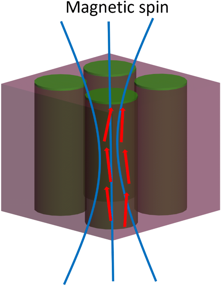 | ||
| Fig. 1 Schematic drawing of the ferromagnetic/superconducting heterostructure design (the red arrows indicate the magnetic moment of Co). | ||
Experimental details
Thin-film growth
The self-assembled thin films were deposited under vacuum using PLD (with a KrF excimer laser, λ = 248 nm). A combined target was used for the deposition. As shown in Fig. S1 (ESI†), a very thin Co strip (∼1 mm) was glued on the NbN target with silver paste. Based on the deposition results, the growth rate of the Co is slightly higher than that of NbN. All the films were deposited under vacuum at 700 °C.Structure and physical-property characterization
The microstructure of the films was characterized using X-ray diffraction (XRD, PANalytical Empyrean), transmission electron microscopy (TEM), and scanning transmission electron microscopy (STEM) (FEI TALOSTM 200FX operated at 200 kV, and FEI TITANTM G2 80–200 with a Cs probe corrector and ChemiSTEMTM technology, operated at 200 kV), and STEM electron-dispersive X-ray spectroscopy (EDS). The magnetic response was measured using a quantum design MPMS-3 SQUID magnetometer. Superconductivity R-T measurements were performed using a physical property measurement system (PPMS) with AC current (through a four-point probe measurement).Results and discussion
The pure NbN film was directly deposited on MgO, and the NbN–Co thin films were fabricated by co-growing Co with NbN under vacuum. The crystal structures of both films were characterized using XRD, as shown in Fig. 2. The XRD patterns of both the NbN and NbN–Co samples show peaks appearing at 2θ = 40.8° and 88.9°. They match very well with the (002) and (004) reflections of face-centered cubic (fcc) NbN (JCPDS no. 38-1155), indicating the NbN(002)//MgO(002) orientation and highly textured film quality. Cubic-phase NbN was also reported to exhibit the best superconductivity among the various NbN crystal structures.14,46 However, Co peaks cannot be identified from the XRD pattern due to the low concentration. It is worth noting that the NbN peak intensity of the NbN–Co thin film is stronger than that of the pure NbN thin film, indicating a better film quality of the NbN–Co thin film than the pure NbN film. To verify the film quality, a rocking curve measurement was conducted on both pure NbN and NbN–Co thin films, and the results are shown in Fig. S2 (ESI†). It is worth noting that there are two sharp peaks from the NbN–Co composite thin film, while only one peak is identified for the pure NbN thin film. The two peaks could be from the two strain states of the NbN in the composite film, the bulk matrix and the strained interface area with Co. The FWHM of the rocking curve of the NbN–Co composite is smaller than that of pure NbN, which proves the better film quality of the NbN–Co composite. This could result from the strain effect, with a similar result having been previously reported by Huang and co-workers.47 Since the lattice parameter of bulk cubic NbN is a = 4.45 Å, which is slightly larger than that of the MgO substrate (a = 4.21 Å), integrating the smaller Co lattice structure inside the NbN thin film can reduce the in-plane strain between the film and the substrate. Besides this, RT measurements were conducted on the pure NbN thin film with a physical property measurement system (PPMS), and the results are shown in Fig. S3 (ESI†). With the temperature decreasing from 200 K to 1.8 K, there is a sharp drop in the resistance (from 2 Ohm to 0 Ohm) around 4 K, indicating that the superconductivity transition temperature is 4 K. | ||
| Fig. 2 XRD of NbN and NbN–Co thin films on MgO; both films show a c-NbN(002)//MgO(002) orientation. | ||
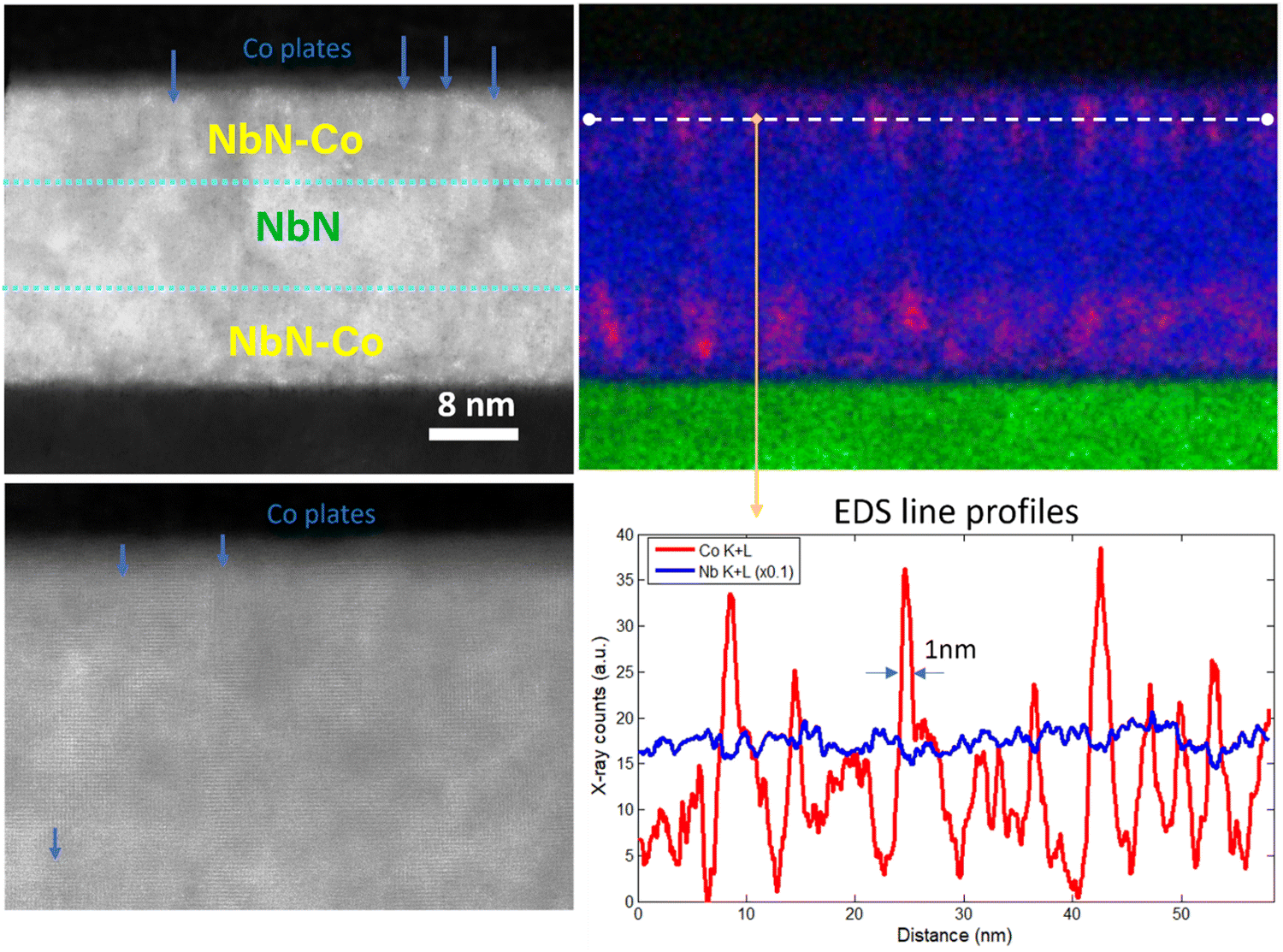
To investigate the morphology and crystal structure, (S)TEM analysis was conducted on both films. The thicknesses of the NbN and NbN–Co films are both around 50 nm. As shown in Fig. S4 (ESI†), the pure NbN thin film is epitaxially grown on the MgO substrate, and the HRSTEM image confirmed that the NbN thin film has a cubic structure, agreeing well with the XRD result. A slight distortion of the lattice structure was also identified in the NbN layer, which could result from the lattice mismatch between NbN and MgO. Further, STEM and EDS analyses were conducted on the NbN–Co film and the results are shown in Fig. 3. Very interestingly, the Co pillars are uniformly distributed inside the NbN matrix. In addition, it was investigated that the Co strip size on the NbN target can highly influence the Co nanoplate growth. As shown in Fig. S5 (ESI†), a larger Co strip would lead to larger Co nanoplates with less spacing, and a thinner Co strip could lead to more ordered Co nanoplates. As shown in Fig. S6 (ESI†), by counting the area of Co nanoplates in the Plan-View (PV) image, the Co concentration can be estimated to be around 16% in volume density, where the EDS composition analysis also agrees with this estimation.
 | ||
Fig. 3 (a) EDS mapping, (b) line profile, and (c) HAADF-STEM image of a cross-section of the NbN–Co thin film. (d) The corresponding FFT of the STEM image in (c). NbN is confirmed to be a cubic structure, and Co is confirmed to be hcp Co. The Co growth direction is [10![[1 with combining macron]](https://www.rsc.org/images/entities/char_0031_0304.gif) 0]. The cross-section image was taken for [010] NbN or [0001] Co. 0]. The cross-section image was taken for [010] NbN or [0001] Co. | ||
Since the Co peaks can hardly be detected via the XRD pattern, high-resolution STEM was performed on the NbN–Co thin film to understand the orientation and crystallinity of the Co pillars. As shown in Fig. 3c, it can be observed that the NbN matrix is still maintained in a single crystal cubic phase with embedded Co pillars, which match well with the XRD result. The crystal structure of Co is confirmed to be hexagonal close packed (hcp) with [100] as the out-of-plane direction (the imaging zone axis of Co is in the [0001] direction). To understand why the Co is grown in such orientation, lattice calculations were conducted, and suggest that the lattice strain between Co and NbN plays an important role. The schematic drawing of the Co orientation is shown in Fig. S7 (ESI†). For the cubic NbN, the lattice parameter is a = 4.45 Å. For the hcp Co, the lattice parameter a = b = 2.51 Å, and c = 4.07 Å. For the fcc Co, the lattice parameter a = 3.54 Å. The d-spacing of the hcp Co (100) plane can be calculated to be 2.17 Å, which is close to one half of the lattice parameter of NbN a = 4.45 Å, and the lattice mismatch is only 2.5%. Also, the d-spacing of the hcp Co (0001) plane can be calculated to be 4.07 Å, which also matches well with the NbN lattice parameter, and the lattice mismatch is around 8.6%. For the fcc Co, the lattice mismatch is very large (22.8%), which can lead to a large strain field inside the thin film. Therefore, a low strain field within in-plane can be achieved when the Co nanopillars are in the hcp structure with the [100] out-of-plane direction. Such a strain relation can explain the preferred orientation of the Co pillars inside the NbN–Co thin film.
PV STEM and EDS analyses were also performed on the NbN–Co sample to examine the distribution of the Co pillars, and the results are shown in Fig. 4. Instead of growing into the typical cylindrical shape (as illustrated in Fig. 1), the Co grows as rectangular nanoplates in two orthogonal orientations along the a- and b-axes of the NbN crystal structure. Based on the HR-STEM image shown in Fig. 4c, it can be observed that, along the longer side of the Co nanoplates, the lattice of Co matches very well with the lattice of the fcc NbN matrix, and the Co orientation is further confirmed to be in the hcp crystal structure with the [100] out-of-plane direction. This plate shape can also be explained by the above lattice misfit calculations. The longer side of the Co nanoplates is along the [0001] direction of the hcp Co crystal with the (0002)Co//(020)NbN and a small misfit of about 2.5%, while the shorter side is along the [11![[2 with combining macron]](https://www.rsc.org/images/entities/char_0032_0304.gif) 0] direction of Co with (110)Co//(200)NbN and a large misfit of 15.4%. With such an orientation and morphology, the total strain energy is highly reduced to make the structure stable. The EDS mapping indicates that the Co plates are very thin with the width of 1 nm, and the length of the plates varied from 5 to 10 nm.
0] direction of Co with (110)Co//(200)NbN and a large misfit of 15.4%. With such an orientation and morphology, the total strain energy is highly reduced to make the structure stable. The EDS mapping indicates that the Co plates are very thin with the width of 1 nm, and the length of the plates varied from 5 to 10 nm.
 | ||
| Fig. 4 (a) and (b) HRSTEM, (c) EDS line scan and (d) EDS mapping of a plan-view sample of the NbN–Co thin film. The Co plates are in two equivalent orientations along the x and y axis of the NbN crystal structure in-plane. The images are taken in the zone axis of [001] NbN or [100] Co. | ||
To examine the influence of the Co nanoplate incorporation, the magnetic response of both NbN and NbN–Co was measured using a magnetic property measurement system (MPMS), and the results are shown in Fig. 5. The pure NbN has no obvious magnetic response, and a strong ferromagnetic response is obtained in the NbN–Co thin film. It is interesting that the magnetic anisotropy of the NbN–Co thin film is not strong, and the coercive field in-plane and out-of-plane is comparable, in the range from −820 Oe to 820 Oe. The coercive field of the NbN-based SC/FM structure has not been reported before, and our coercive field range is comparable with some YBCO-based and Nb-based multi-layer SC/FM structures.48–51 This magnetic anisotropy is weaker than that of cylindrical Co nanopillars reported previously in a Co–ZrO2 VAN system.42 This is perhaps due to the nanoplates having one dimension approaching the paramagnetic limit, which results in a lower magnetic response. This could be attributed to the unique shape of the Co nanostructures, because the Co nanostructure grows with the nanoplates and those nanoplates have two orientations that are perpendicular to each other. Such a plate-like shape makes the in-plane and out-of-plane response comparable. The ferromagnetic response indicates that we have successfully implanted the magnetic dipole inside the NbN thin film with Co nanoplates.
 | ||
| Fig. 5 Magnetic response of pure NbN and NbN–Co thin films grown on a MgO (001) substrate: (a) out-of-plane (OP) M–H loop measured at 300 K for NbN, (b) OP M–H loop measured at 10 K for NbN, (c) in-plane (IP) and OP M–H loops measured at 300 K for NbN–Co, and (d) IP and OP M–H loops measured at 10 K for NbN–Co (with correction factors applied). | ||
The size and density of the Co nanoplate can influence both the magnetic and superconducting performance. If the Co nanoplates become thinner and longer, the out-of-plane magnetic anisotropy could become stronger. If the spacing between Co nanoplates becomes smaller, the Co concentration could increase, leading to a stronger magnetic response. However, such a high Co concentration could also further reduce the superconducting performance of the overall NbN–Co films. Therefore, maintaining a good balance in the Co concentration between magnetic response and superconductivity is important.
Such magnetic and superconducting hybrid structures in NbN have not been previously reported. In previous reports, some attempts of FM/SC have been reported for other superconductors using other means, such as impurity doping,52,53 multi-layer structures,54,55 and nanoparticles on the surface.56,57 Previous reports point out that the magnetic flux pinning effect from the interaction between a ferromagnet and superconductor plays an important role.58–60 The reasons to select Co nanoplates for this case are: (1) secondary phase incorporation could have fewer impacts on the overall structural and superconducting properties of the matrix than addition of dopants. In this work, the Co nanoplates are growing epitaxially in the NbN matrix and have minimal impacts on the structure; (2) the anisotropic Co nanoplates could also introduce out-of-plane magnetic anisotropy, while uniform doping is an isotropic method. Therefore, compared with the previous reports, of either impurity doping or nanoparticles on the surface, the epitaxial NbN–Co nanocomposite structure in this work can generate a more ordered magnetic field.
In addition, Co is a type of plasmonic material. Therefore, the optical response was characterized. As shown in Fig. S8 (ESI†), the permittivity of the pure NbN on MgO is consistent with other NbN thin films previously reported.61 NbN–Co exhibits strong Type-II hyperbolic dispersion, i.e., the in-plane permittivity is negative and the out-of-plane permittivity is positive, which indicates the strong optical anisotropy of this unique structure.
Furthermore, the TEM characterization indicates that the NbN matrix is in a single crystal phase, which offers more opportunity for epitaxial growth with other materials. To confirm this, a multilayer structure of a NbN–Co/NbN thin film was fabricated, and the TEM characterization results are shown in Fig. 6. The HRSTEM indicates that the NbN–Co layer can grow over the NbN layer with cube-on-cube epitaxy, where the NbN is in a single crystal-like cubic structure throughout the entire film. In addition, the size and pillar–pillar distance of the Co nanoplates are on the nanometer scale, which is much smaller than that in previous reported work, and this can lead to better interaction with the superconductor.58,62 With such a unique structure and magnetic response, it could be coupled with the superconductivity of the NbN thin film to be applied in the quantum computing field.
 | ||
| Fig. 6 HRSTEM and EDS mapping of a cross-section of the NbN–Co/Nb/NbN–Co multilayer thin film. High epitaxial quality can be detected from the multilayer structure. | ||
Conclusion
In summary, NbN and NbN–Co thin films have been successfully deposited on a MgO substrate with a cube-on-cube epitaxy between the NbN matrix and the MgO substrate. The obtained pure NbN thin film exhibits superconductivity at ∼4 K. In the NbN–Co thin film, the Co is in the hcp crystal structure, and it grows with the nanoplates embedded inside the NbN matrix in the [100] out-of-plane direction. Based on our calculations, such orientation can greatly reduce the in-plane lattice-misfit and the adaptation of the plate geometry minimizes total strain energy in the film. By incorporating the Co nanoplates inside the NbN thin film, a strong ferromagnetic response can be detected from the NbN–Co thin film, and the unique hybrid nanocomposite generates a domain-like magnetic dipole on each Co plate. Such structure may be applied in future superconducting spintronic devices and quantum computing devices.
In addition, to achieve better superconducting properties, the growth conditions of both pure NbN and NbN–Co thin films shall be further optimized to minimize the potential poisoning effects from Co. In addition, other potential ferromagnetic materials could be explored in the future beyond Co, such as Fe, Ni and Ni80Fe20. These new ferromagnetic nanoinclusions may exhibit similar properties within such a unique structure.
Data availability
The data supporting this article has been included as part of the ESI.†Conflicts of interest
There are no conflicts to declare.Acknowledgements
This work was supported by the U.S. National Science Foundation DMR-2016453 (nitride growth and high resolution TEM/STEM). B. T., J. S. and H. W. acknowledge the support from DMREF-2323753 (for integration and property measurements). Y. Z. and H. W. also acknowledge the user facility of the Center of Integrated Technology Center (CINT) for microscopy access and support. The microscopy work was partially supported by the Laboratory Directed Research and Development program at Sandia National Laboratories. Sandia National Laboratories is a multi-mission laboratory managed and operated by National Technology and Engineering Solutions of Sandia, LLC., a wholly owned subsidiary of Honeywell International, Inc., for the U.S. Department of Energy's National Nuclear Security Administration under contract no. DE-NA0003525. This paper describes objective technical results and analysis. Any subjective views or opinions that might be expressed in the paper do not necessarily represent the views of the U.S. Department of Energy or the United States Government.References
- Y. Makhlin, G. Scöhn and A. Shnirman, Josephson-junction qubits with controlled couplings, Nature, 1999, 398, 305–307 CrossRef CAS.
- Y. Makhlin, G. Schön and A. Shnirman, Quantum-state engineering with Josephson-junction devices, Rev. Mod. Phys., 2001, 73, 357 CrossRef.
- K. Lang, S. Nam, J. Aumentado, C. Urbina and J. M. Martinis, Banishing quasiparticles from Josephson-junction qubits: Why and how to do it, IEEE Trans. Appl. Supercond., 2003, 13, 989–993 CrossRef CAS.
- N. Yabuki, R. Moriya, M. Arai, Y. Sata, S. Morikawa, S. Masubuchi and T. Machida, Supercurrent in van der Waals Josephson junction, Nat. Commun., 2016, 7, 10616 CrossRef CAS PubMed.
- L. Zeng, S. Nik, T. Greibe, P. Krantz, C. Wilson, P. Delsing and E. Olsson, Direct observation of the thickness distribution of ultra thin AlOx barriers in Al/AlOx/Al Josephson junctions, J. Phys. D: Appl. Phys., 2015, 48, 395308 CrossRef.
- S. I. Morohashi and S. Hasuo, Experimental investigations and analysis for high-quality Nb/Al–AlOx/Nb Josephson junctions, J. Appl. Phys., 1987, 61, 4835–4849 CrossRef CAS.
- J. Du, J. Lazar, S. Lam, E. Mitchell and C. Foley, Fabrication and characterisation of series YBCO step-edge Josephson junction arrays, Supercond. Sci. Technol., 2014, 27, 095005 CrossRef CAS.
- H. Shimakage, K. Tsujimoto, Z. Wang and M. Tonouchi, Characteristics of MgB2/AlN/NbN Josephson junctions with optimized conditions, Supercond. Sci. Technol., 2004, 17, 1376 CrossRef CAS.
- S. Kim, H. Terai, T. Yamashita, W. Qiu, T. Fuse, F. Yoshihara, S. Ashhab, K. Inomata and K. Semba, Enhanced coherence of all-nitride superconducting qubits epitaxially grown on silicon substrate, Commun. Mater., 2021, 2, 98 CrossRef CAS.
- Q. Zhang, H. Wang, X. Tang, H. Xue, W. Peng and Z. Wang, Josephson tunneling behaviors in NbN/AlN/NbN junctions with an ultrathin NbN film, IEEE Trans. Appl. Supercond., 2018, 28, 1–4 Search PubMed.
- Y. Nakamura, H. Terai, K. Inomata, T. Yamamoto, W. Qiu and Z. Wang, Superconducting qubits consisting of epitaxially grown NbN/AlN/NbN Josephson junctions, Appl. Phys. Lett., 2011, 99, 212502 CrossRef.
- S. Chockalingam, M. Chand, J. Jesudasan, V. Tripathi and P. Raychaudhuri, Superconducting properties and Hall effect of epitaxial NbN thin films, Phys. Rev. B: Condens. Matter Mater. Phys., 2008, 77, 214503 CrossRef.
- M. S. Hossain, K. Yoshida, K. Kudo, K. E. K. Enpuku and K. Y. K. Yamafuji, Enlargement of kinetic inductance of NbN superconducting thin films for device applications, Jpn. J. Appl. Phys., 1992, 31, 1033 CrossRef CAS.
- Z. Wang, A. Kawakami, Y. Uzawa and B. Komiyama, Superconducting properties and crystal structures of single-crystal niobium nitride thin films deposited at ambient substrate temperature, J. Appl. Phys., 1996, 79, 7837–7842 CrossRef CAS.
- X. Wei, P. Roy, Z. Yang, D. Zhang, Z. He, P. Lu, O. Licata, H. Wang, B. Mazumder and N. Patibandla, Ultrathin epitaxial NbN superconducting films with high upper critical field grown at low temperature, Mater. Res. Lett., 2021, 9, 336–342 CrossRef CAS.
- A. Verevkin, J. Zhang, R. Sobolewski, A. Lipatov, O. Okunev, G. Chulkova, A. Korneev, K. Smirnov, G. Gol’tsman and A. Semenov, Detection efficiency of large-active-area NbN single-photon superconducting detectors in the ultraviolet to near-infraredrange, Appl. Phys. Lett., 2002, 80, 4687–4689 CrossRef CAS.
- A. Korneev, P. Kouminov, V. Matvienko, G. Chulkova, K. Smirnov, B. Voronov, G. Gol’tsman, M. Currie, W. Lo and K. Wilsher, Sensitivity and gigahertz counting performance of NbN superconducting single-photon detectors, Appl. Phys. Lett., 2004, 84, 5338–5340 CrossRef CAS.
- K. Smirnov, A. Divochiy, Y. Vakhtomin, P. Morozov, P. Zolotov, A. Antipov and V. Seleznev, NbN single-photon detectors with saturated dependence of quantum efficiency, Supercond. Sci. Technol., 2018, 31, 035011 CrossRef.
- L. Kang, B. Jin, X. Liu, X. Jia, J. Chen, Z. Ji, W. Xu, P. Wu, S. Mi and A. Pimenov, Suppression of superconductivity in epitaxial NbN ultrathin films, J. Appl. Phys., 2011, 109, 033908 CrossRef.
- T. Roch, M. Gregor, S. Volkov, M. Čaplovičová, L. Satrapinskyy and A. Plecenik, Substrate dependent epitaxy of superconducting niobium nitride thin films grown by pulsed laser deposition, Appl. Surf. Sci., 2021, 551, 149333 CrossRef CAS.
- S. Y. Jang, H. M. Lee, J. Y. Sung, S. E. Kim, J. D. Jeon, Y. Yun, S. M. Moon, J. E. Yoo, J. H. Choi and T. J. Park, Epitaxial growth of NbN thin films for electrodes using atomic layer deposition, Appl. Surf. Sci., 2023, 636, 157824 CrossRef.
- F. Mercier, S. Coindeau, S. Lay, A. Crisci, M. Benz, T. Encinas, R. Boichot, A. Mantoux, C. Jimenez and F. Weiss, Niobium nitride thin films deposited by high temperature chemical vapor deposition, Surf. Coatings Technol., 2014, 260, 126–132 CrossRef CAS.
- R. E. Treece, J. S. Horwitz, J. H. Claassen and D. B. Chrisey, Pulsed laser deposition of high-quality NbN thin films, Appl. Phys. Lett., 1994, 65, 2860–2862 CrossRef CAS.
- J. Bardeen, L. N. Cooper and J. R. Schrieffer, Microscopic theory of superconductivity, Phys. Rev. Appl., 1957, 106, 162 CAS.
- A. Gaita-Ariño, F. Luis, S. Hill and E. Coronado, Molecular spins for quantum computation, Nat. Chem., 2019, 11, 301–309 CrossRef PubMed.
- W. D. Oliver and P. B. Welander, Materials in superconducting quantum bits, MRS Bull., 2013, 38, 816–825 CrossRef CAS.
- M. He, H. Sun and Q. L. He, Topological insulator: Spintronics and quantum computations, Front. Phys., 2019, 14, 1–16 Search PubMed.
- A. P. Mackenzie and Y. Maeno, The superconductivity of Sr2RuO4 and the physics of spin-triplet pairing, Rev. Mod. Phys., 2003, 75, 657 CrossRef CAS.
- S. Ran, C. Eckberg, Q.-P. Ding, Y. Furukawa, T. Metz, S. R. Saha, I.-L. Liu, M. Zic, H. Kim and J. Paglione, Nearly ferromagnetic spin-triplet superconductivity, Science, 2019, 365, 684–687 CrossRef CAS PubMed.
- T. Maniv, V. Zhuravlev, I. Vagner and P. Wyder, Vortex states and quantum magnetic oscillations in conventional type-II superconductors, Rev. Mod. Phys., 2001, 73, 867 CrossRef CAS.
- D. Brawner and H. Ott, Evidence for an unconventional superconducting order parameter in YBa2Cu3O6.9, Phys. Rev. B: Condens. Matter Mater. Phys., 1994, 50, 6530 CrossRef PubMed.
- M. Milošević and F. Peeters, Vortex-antivortex lattices in superconducting films with magnetic pinning arrays, Phys. Rev. Lett., 2004, 93, 267006 CrossRef PubMed.
- M. Vélez, J. Martin, J. Villegas, A. Hoffmann, E. González, J. Vicent and I. K. Schuller, Superconducting vortex pinning with artificial magnetic nanostructures, J. Magn. Magn. Mater., 2008, 320, 2547–2562 Search PubMed.
- S. Frolov, M. Manfra and J. Sau, Topological superconductivity in hybrid devices, Nat. Phys., 2020, 16, 718–724 Search PubMed.
- J.-X. Yin, B. Lian and M. Z. Hasan, Topological kagome magnets and superconductors, Nature, 2022, 612, 647–657 CrossRef CAS PubMed.
- D. H. Kim, S. Ning and C. A. Ross, Self-assembled multiferroic perovskite–spinel nanocomposite thin films: epitaxial growth, templating and integration on silicon, J. Mater. Chem. C, 2019, 7, 9128–9148 RSC.
- J. Huang, L. Li, P. Lu, Z. Qi, X. Sun, X. Zhang and H. Wang, Self-assembled Co–BaZrO3 nanocomposite thin films with ultra-fine vertically aligned Co nanopillars, Nanoscale, 2017, 9, 7970–7976 RSC.
- Z. Qi, J. Jian, J. Huang, J. Tang, H. Wang, V. G. Pol and H. Wang, LiNi0.5Mn0.3Co0.2O2/Au nanocomposite thin film cathode with enhanced electrochemical properties, Nano Energy, 2018, 46, 290–296 CrossRef CAS.
- Z. Hu, J. Lu, H. Dou, J. Shen, J. P. Barnard, J. Liu, X. Zhang and H. Wang, Template-assisted growth of Co–BaTiO3 vertically aligned nanocomposite thin films with strong magneto-optical coupling effect, Nano Res., 2024, 17, 3130–3138 Search PubMed.
- J. Huang, X. Wang, N. L. Hogan, S. Wu and H. Wang, Nanoscale Artificial Plasmonic Lattice in Self Assembled Vertically Aligned Nitride–Metal Hybrid Metamaterials, Adv. Sci., 2018, 5, 1800416 CrossRef PubMed.
- Y. Zhang, J. Shen, B. K. Tsai, X. Sheng, Z. Hu, X. Zhang and H. Wang, TiN–Au/HfO2–Au Multilayer Thin Films with Tunable Hyperbolic Optical Response, Small Methods, 2024, 2400087 Search PubMed.
- Y. Zhang, J. Song, P. Lu, J. Deitz, D. Zhang, H. Dou, J. Shen, Z. Hu, X. Zhang and H. Wang, Tunable Magnetic and Optical Anisotropy in ZrO2–Co Vertically Aligned Nanocomposites, Adv. Mater. Interfaces, 2023, 10, 2300150 CrossRef CAS.
- D. Zhang, S. Misra, J. Jian, P. Lu, L. Li, A. Wissel, X. Zhang and H. Wang, Self-Assembled BaTiO3–AuxAg1−x Low-Loss Hybrid Plasmonic Metamaterials with an Ordered “Nano-Domino-like” Microstructure, ACS Appl. Mater. Interfaces, 2021, 13, 5390–5398 CrossRef CAS PubMed.
- D. Zhang, S. Misra, L. Li, X. Wang, J. Jian, P. Lu, X. Gao, X. Sun, Z. Qi and M. Kalaswad, Tunable Optical Properties in Self-Assembled Oxide-Metal Hybrid Thin Films via Au-Phase Geometry Control: From Nanopillars to Nanodisks, Adv. Opt. Mater., 2020, 8, 1901359 CrossRef CAS.
- X. Wang, J. Jian, S. Diaz-Amaya, C. E. Kumah, P. Lu, J. Huang, D. G. Lim, V. G. Pol, J. P. Youngblood and A. Boltasseva, Hybrid plasmonic Au–TiN vertically aligned nanocomposites: a nanoscale platform towards tunable optical sensing, Nanoscale Adv., 2019, 1, 1045–1054 Search PubMed.
- Y. Zou, X. Qi, C. Zhang, S. Ma, W. Zhang, Y. Li, T. Chen, X. Wang, Z. Chen and D. Welch, Discovery of superconductivity in hard hexagonal ε-NbN, Sci. Rep., 2016, 6, 22330 CrossRef CAS PubMed.
- J. Huang, J. L. MacManus-Driscoll and H. Wang, New epitaxy paradigm in epitaxial self-assembled oxide vertically aligned nanocomposite thin films, J. Mater. Res., 2017, 32, 4054–4066 CrossRef CAS.
- M. Sousa, A. Honorato, L. Liu, I. Merino, M. Pessoa, P. Morais, F. Litterst, E. Passamani, M. Fontes and E. Baggio-Saitovitch, Static and dynamic magnetic behavior of YBCO/Co/IrMn heterostructures, J. Appl. Phys., 2024, 135, 133901 CrossRef CAS.
- R. de Andrés Prada, R. Gaina, N. Biškup, M. Varela, J. Stahn and C. Bernhard, Controlling the strength of ferromagnetic order in YBa2Cu3O7/La2/3Ca1/3MnO3 multilayers, Phys. Rev. B, 2019, 100, 115129 CrossRef.
- D. Stamopoulos, E. Aristomenopoulou and E. Manios, Absolute supercurrent switch in ferromagnetic/superconducting/ferromagnetic trilayers operating at T > 4.2 K, Appl. Phys. Lett., 2014, 105, 112602 CrossRef.
- R. Steiner and P. Ziemann, Magnetic switching of the superconducting transition temperature in layered ferromagnetic/superconducting hybrids: Spin switch versus stray field effects, Phys. Rev. B: Condens. Matter Mater. Phys., 2006, 74, 094504 CrossRef.
- A. Bawa, R. Jha and S. Sahoo, Tailoring phase slip events through magnetic doping in superconductor-ferromagnet composite films, Sci. Rep., 2015, 5, 13459 CrossRef CAS PubMed.
- K. Jin, J. Yuan, L. Zhao, H. Wu, X. Qi, B. Zhu, L. Cao, X. Qiu, B. Xu and X. Duan, Coexistence of superconductivity and ferromagnetism in a dilute cobalt-doped La1.89Ce0.11CuO4±δ system, Phys. Rev. B: Condens. Matter Mater. Phys., 2006, 74, 094518 CrossRef.
- L. Tagirov, Low-field superconducting spin switch based on a superconductor/ferromagnet multilayer, Phys. Rev. Lett., 1999, 83, 2058 CrossRef CAS.
- L. Bulaevskii, E. Chudnovsky and M. Maley, Magnetic pinning in superconductor-ferromagnet multilayers, Appl. Phys. Lett., 2000, 76, 2594–2596 CrossRef CAS.
- T. Wang, S. Lourette, S. R. O’Kelley, M. Kayci, Y. Band, D. F. J. Kimball, A. O. Sushkov and D. Budker, Dynamics of a ferromagnetic particle levitated over a superconductor, Phys. Rev. Appl., 2019, 11, 044041 CrossRef CAS.
- Y. Nozaki, Y. Otani, K. Runge, H. Miyajima, B. Pannetier, J. P. Nozières and G. Fillion, Magnetic flux penetration process in two-dimensional superconductor covered with ferromagnetic particle array, J. Appl. Phys., 1996, 79, 8571–8577 CrossRef CAS.
- M. Van Bael, L. Van Look, M. Lange, J. Bekaert, S. Bending, A. Grigorenko, K. Temst, V. Moshchalkov and Y. Bruynseraede, Ferromagnetic pinning arrays, Phys. C, 2002, 369, 97–105 CrossRef CAS.
- X. Zhang, G. Wen, R. Zheng, G. Xiong and G. Lian, Enhanced flux pinning in a high-TC superconducting film by a ferromagnetic buffer layer, Europhys. Lett., 2001, 56, 119 CrossRef CAS.
- T. Matsushita, Flux pinning in superconductors, Springer, 2007 Search PubMed.
- A. Semenov, B. Günther, U. Böttger, H.-W. Hübers, H. Bartolf, A. Engel, A. Schilling, K. Ilin, M. Siegel and R. Schneider, Optical and transport properties of ultrathin NbN films and nanostructures, Phys. Rev. B: Condens. Matter Mater. Phys., 2009, 80, 054510 CrossRef.
- T. Alden and J. Livingston, Ferromagnetic particles in a type-II superconductor, J. Appl. Phys., 1966, 37, 3551–3556 CrossRef CAS.
Footnote |
| † Electronic supplementary information (ESI) available. See DOI: https://doi.org/10.1039/d4mh01281j |
| This journal is © The Royal Society of Chemistry 2025 |