
 Open Access Article
 This Open Access Article is licensed under a
 Creative Commons Attribution 3.0 Unported Licence
Photo-crosslinkable organic materials for flexible and stretchable electronics
Minsung
Kim†
 ,
Hayeong
Park†
,
Eunjin
Kim
,
Minji
Chung
and
Joon Hak
Oh
*
,
Hayeong
Park†
,
Eunjin
Kim
,
Minji
Chung
and
Joon Hak
Oh
*
School of Chemical and Biological Engineering, Institute of Chemical Processes, Seoul National University, 1 Gwanak-ro, Gwanak-gu, Seoul 08826, Republic of Korea. E-mail: joonhoh@snu.ac.kr
First published on 20th March 2025
Abstract
As technology advances to enhance human perceptual experiences of the surrounding environment, significant research on stretchable electronics is actively progressing, spanning from the synthesis of materials to their applications in fully integrated devices. A critical challenge lies in developing materials that can maintain their electrical properties under substantial stretching. Photo-crosslinkable organic materials have emerged as a promising solution due to their ability to be precisely modified with light to achieve desired properties, such as enhanced durability, stable conductivity, and micropatterning. This review examines recent research on photo-crosslinkable organic materials, focusing on their components and integration within stretchable electronic devices. We explore the essential characteristics required for each device component (insulators, semiconductors, and conductors) and explain how photo-crosslinking technology addresses these needs through its principles and implementation. Additionally, we discuss the integration and utilization of these components in real-world applications, including physical sensors, organic field-effect transistors (OFETs), and organic solar cells (OSCs). Finally, we offer a concise perspective on the future directions and potential challenges in ongoing research on photo-crosslinkable organic materials.
 Minsung Kim | Minsung Kim received his BS degree from the School of Chemical and Biological Engineering at Seoul National University in 2021. He is currently enrolled in the MS/PhD program in the School of Chemical and Biological Engineering at Seoul National University, under the supervision of Prof. Joon Hak Oh. His research interests include synthesis of elastomers and their applications. |
 Hayeong Park | Hayeong Park received her BS degree from the School of Chemical Engineering at Sungkyunkwan University in 2021. She is currently enrolled in the MS/PhD program in the School of Chemical and Biological Engineering at Seoul National University, under the supervision of Prof. Joon Hak Oh. Her research interests include fully stretchable OFETs and circuit applications. |
 Eunjin Kim | Eunjin Kim received her BS degree from the Department of Chemical Engineering at Pohang University of Science and Technology in 2023. She is currently enrolled in the MS program in the School of Chemical and Biological Engineering at Seoul National University, under the supervision of Prof. Joon Hak Oh. Her research focuses on stretchable OFETs and circuit applications. |
 Minji Chung | Minji Chung received her BS degree from the School of Chemical and Biological Engineering at Seoul National University in 2024. She is currently enrolled in the MS/PhD program in the School of Chemical and Biological Engineering at Seoul National University, under the supervision of Prof. Joon Hak Oh. Her research interests include the processing of organic/polymer semiconductors for stretchable field-effect transistors. |
 Joon Hak Oh | Joon Hak Oh is a professor at the School of Chemical and Biological Engineering, Seoul National University, where he received his PhD degree (2004). He conducted his postdoctoral research in the Department of Chemical Engineering at Stanford University (2006–2010). He worked as an assistant professor at the School of Energy and Chemical Engineering at Ulsan National Institute of Science and Technology (2010–2014) and an associate professor in the Department of Chemical Engineering at Pohang University of Science and Technology (2014–2018). His research interests include organic/polymer electronics, advanced optoelectronics with chiral and perovskite materials, and multifunctional sensors. |
Wider impactIn flexible and stretchable electronics, photo-crosslinking technology is a powerful technique that enables precise control over the structure of organic materials using specific wavelengths of light. This technique allows for achieving an optimal balance between the mechanical durability and electrical properties. However, there remains a lack of comprehensive reviews summarizing the role of photo-crosslinking in the design of organic materials and their integration into electronic devices. This review aims to fill that gap by analysing key challenges faced by components in stretchable electronics and demonstrating how photo-crosslinking strategies can be used to overcome these obstacles. It also examines recent breakthroughs in material integration, illustrating how this technology enhances the reliability and performance of the devices. By combining structural precision with advanced functionalities, particularly when coupled with additive manufacturing techniques like 3D printing, photo-crosslinking holds immense potential to accelerate the development of stretchable electronics. These advancements are anticipated to drive innovation across diverse industries, including healthcare, environmental monitoring, and energy, ultimately contributing to improving quality of life. We hope this review inspires novel approaches in materials science and provides researchers with valuable insights to propel the advancements in next-generation stretchable electronics. |
1. Introduction
The digital revolution is fundamentally transforming our lifestyles and redefining how we interact with technology and communicate with one another. These changes are driving significant advancements in the design and functionality of electronic devices, making them more versatile and user-friendly than ever before. Among these developments, stretchable electronics are leading the way, providing immersive experiences that distinguish them from traditional rigid devices.1–3 Stretchable electronics represent not just a gradual improvement in performance, but also a paradigm shift that fundamentally changes our approach to electronic interfaces and applications.Unlike traditional rigid electronic devices, stretchable electronics can adapt to various shapes and surfaces, allowing them to be attached anywhere and worn comfortably. This flexibility enables an unprecedented user experience and functionality, leading to innovative applications across various fields. For example, in the medical and healthcare field, body-attached electronic devices are utilized in wearable health monitors that track vital signs in real time, providing valuable data for both patients and healthcare providers.4–6 In robotics, these devices enhance the responsiveness of robots, allowing for more refined interactions with their environments.7,8 Furthermore, in the field of energy storage, stretchable batteries and supercapacitors are integrated into flexible materials, offering more efficient and adaptable energy solutions.9–11 Additionally, stretchable electronics play a crucial role in environmental monitoring,12–14 enabling the collection of air and water quality data across various environments to facilitate rapid responses to ecological changes. In this way, the emergence of stretchable electronics has a wide-ranging impact across industries and daily life.
For the development of stretchable electronics, two different approaches have been primarily investigated: i.e., structure-based approaches and material-based approaches.15 The structure-based approaches achieve stretchability through geometric patterns and structure designs such as kirigami, origami, and mesh structures.16–22 However, the complexity of structure designs can complicate the manufacturing process, making it less suitable for large-scale production.23 Moreover, geometric design typically restricts deformation to specific directions, which limits the potential for multi-directional flexibility.24,25
On the other hand, the material-based approaches focus on the precise design of material structures and compositions to obtain desired properties. These approaches allow for the adjustment of the inherent characteristics of the materials through molecular design, ensuring that electronic devices maintain stability even under continuous deformation.26 Notably, this approach can be tailored to consider biocompatibility with human tissues, thereby contributing to the reliability and safety of electronic devices, particularly in medical and biomedical implant applications.27–29
In the material-based approaches, organic materials have become essential materials due to their unique intrinsic properties: excellent elasticity, light weight, and durability.30 These superior properties of polymers allow devices remain durable under mechanical stimuli. This capability allows for a wide range of applications, from smart clothing to implantable devices that conformally attach to internal organs.
Currently, many researchers are making continuous efforts to balance the mechanical and electrical properties of organic materials for stretchable electronics. Among the various methods to achieve this balance, photo-crosslinking is gaining significant attention. Photo-crosslinking utilizes light with specific wavelengths to rapidly form covalent bonds between organic materials. This technique allows for precise tuning and low-temperature processing, making it easy to modify the properties of soft materials. As a result, it is widely used in the research of stretchable electronics.
In the following, we will explore the utilization of photo-crosslinking technology in stretchable electronic devices (Fig. 1). We will begin by outlining the strategies for incorporating photo-crosslinkable components in stretchable electronics into three main categories: insulators, semiconductors, and conductors. We will discuss the chemical structures and mechanisms behind the application of photo-crosslinking technology to each component. Next, we will highlight how these three elements integrate into a combined device, working together to optimize performance. Through various applications of stretchable electronic devices – such as physical sensors, organic field-effect transistors (OFETs), and organic solar cells (OSCs) – we will examine how these elements interact to enhance the performance of the integrated system, thereby demonstrating the practicality and potential of photo-crosslinking technology. Finally, we will discuss the opportunities that photo-crosslinking technology offers in the field of stretchable electronics.
 | ||
| Fig. 1 Schematic illustration of photo-crosslinkable components and their applications in flexible and stretchable electronics. Image of “substrate”31 Copyright 2021, The American Association for the Advancement of Science. Image for “dielectric”32 Copyright 2017, American Chemical Society. Image for “adhesive”33 Copyright 2024, Elsevier. Image for “ion conductive”34 Copyright 2022, American Chemical Society. Image for “liquid metal”35 Copyright 2023, Wiley-VCH. Image for “organic solar cells”36 Copyright 2019, Wiley-VCH. Image for “OFET multi-array”37 Copyright 2021, Springer Nature. Image for “E-Skin”38 Copyright 2023, The American Association for the Advancement of Science. Image for “strain-insensitive pressure sensor”39 Copyright 2024, Wiley-VCH. Image for “pressure sensor multi-array”40 Copyright 2022, American Chemical Society. | ||
2. Photo-crosslinking technology mechanisms
Photo-crosslinking technology is a simple method to modify the physical and chemical properties of organic materials by employing light to induce covalent bonds between polymer chains or molecular components (Fig. 2). Typically, this process involves the generation of reactive intermediates (e.g., radical, ion, carbene, etc.) via light activation. These intermediates then engage in subsequent reactions to form robust crosslinks, setting the stage for a wide variety of material transformations.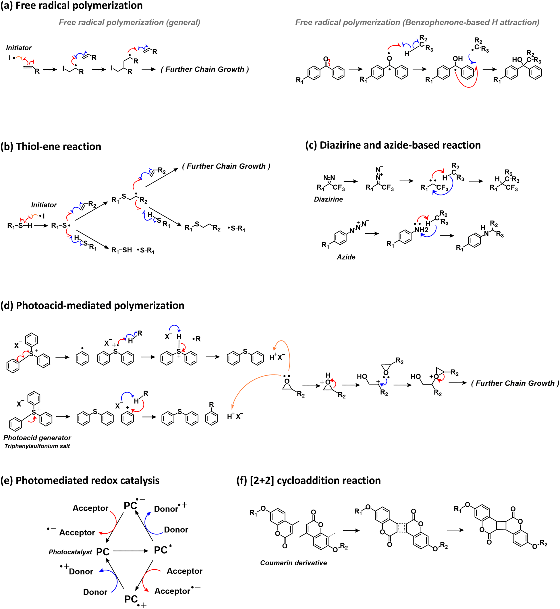 | ||
| Fig. 2 Schematic representation of various photo-crosslinking mechanisms. (a) Free radical polymerization. (b) Thiol-ene reaction. (c) Diazirine and azide-based reaction. (d) Photoacid-mediated polymerization. (e) Photomediated redox catalysis. (f) [2+2] cycloaddition reaction. | ||
A common example of this approach is free radical polymerization. In such systems, a photoinitiator absorbs UV or visible light and transitions to an excited state. This excited state weakens internal bonds, leading to their cleavage and the formation of free radicals. These radicals then add to C–C unsaturated bonds, initiating chain propagation and eventually combining to form a stable crosslinked network.41,42 Similarly, benzophenone-based hydrogen abstraction utilizes light in a related mechanism. Upon absorbing light, benzophenone reaches an excited triplet state that abstracts a hydrogen atom from a nearby polymer chain's C–H bond. The resulting polymer radical can then either couple with another radical or participate in further reactions, effectively forming crosslinks without requiring an additional initiator.43–45
Expanding on radical-based processes, the thiol–ene reaction represents another effective photo-crosslinking pathway. Here, light activates a thiol (–SH) group to produce a thiyl radical. This radical promptly adds to a C–C unsaturated bond, generating a carbon-centered radical that subsequently reacts with another thiol. Through repeated cycles, this mechanism gradually builds a uniform and resilient crosslinked network.46,47
Beyond these radical mechanisms, diazirine and azide-based photocrosslinking reactions exploit light to generate highly reactive intermediates without the need for a separate initiator. Upon exposure to light, these functional groups release small molecules such as nitrogen, thereby producing reactive carbene or nitrene intermediates. These intermediates rapidly insert into C–H bonds or other reactive sites on the polymer chain, directly forming crosslinks.48–52
Photoacid-mediated crosslinking represents a unique strategy for forming covalent polymer networks through the controlled release of acid. In this process, the photoacid generator (PAG) absorbs light to reach a high-energy state and subsequently undergoes bond cleavage to release acid. This acid protonates acid-sensitive monomers (e.g., epoxides, vinyl ethers, etc.), generating active intermediates that react with adjacent monomers to gradually build a covalent network. This mechanism can initiate either ring-opening or step-growth polymerization via nucleophilic substitution. Unlike radical polymerization, photoacid-mediated reactions are insensitive to atmospheric oxygen and do not involve termination reactions, resulting in high curing efficiency and the formation of diverse polymer backbones.53 PAGs are generally classified into ionic and non-ionic types. Ionic PAGs are typically based on onium salt derivatives (e.g., diaryliodonium salts, sulfonium salts, etc.). When exposed to light, they generate acid via direct π–σ* or π–π* transitions or by intersystem crossing to the triplet state, followed by either heterolytic or homolytic bond cleavage.54,55 In these systems, the cation determines the photochemical reactivity and thermal stability, while the counter-anion (e.g., BF4−, PF6−, and SbF6−) controls the acid strength and the rate of polymerization initiation.56,57 However, ionic PAGs often exhibit limited solubility in reactive monomers or organic solvents.53,58 Additionally, they often require thicker films to ensure sufficient radiation absorption and may pose potential issues related to toxicity and external band reactivity.59–61 To overcome these limitations, non-ionic PAGs have attracted significant attention. Under illumination, the C–O, S–O, and N–O bonds in non-ionic PAGs (e.g., imido sulfonate, arylsulfonate esters, etc.) undergo dissociation, forming structurally stabilized radicals. These radicals then extract hydrogen from protic solvents, leading to the generation of acidic compounds. Their excellent solubility in various solvents and polymer matrices makes them particularly useful for photopolymerization and surface curing applications.62–64 Although non-ionic PAGs are generally less thermally stable than their ionic PAGs, this drawback has been effectively mitigated through careful modification of pendant structures within their molecular frameworks.65
Photomedicated redox catalysts provide an alternative pathway for generating active intermediates that lead to crosslink formation. In this method, catalysts (e.g., Ru(bpy)32+, Ir(ppy)3, etc.) absorb light and transition to an excited state, resulting in significant changes in their electronic structures that enhance their electron-donating and electron-accepting abilities. The excited catalyst interacts with redox-active groups in the reactants, inducing electron transfer that converts stable reactants into highly reactive radical species or radical ions. These reactive intermediates combine to form crosslinks, while the catalyst is regenerated through additional electron transfer, thereby sustaining an efficient polymerization cycle.66–68 For optimal performance, the redox potentials of the catalyst and reactants must be well-matched to facilitate efficient electron transfer and selective crosslinking while minimizing side reactions. Furthermore, a sufficiently long excited state lifetime is essential to enable efficient electron or hydrogen transfer between donors and acceptors. Additionally, achieving both high photoluminescence quantum efficiency and excellent reversibility is essential for efficient catalyst recycling.66,68–71
While many photo-crosslinking reactions proceed generating reactive intermediates that then form crosslinks, some reactions rely on direct bonding between excited state groups. A prominent example of this is the [2+2] cycloaddition reaction. In this process, a light-activated functional group undergoes a π → π* transition, and when two such excited groups are correctly aligned, they simultaneously form two σ bonds to create a four-membered cyclobutane ring.72 Notably, certain [2+2] cycloaddition systems (e.g., coumarin, cinnamate, thymine, etc.) are reversible. Under specific wavelengths of light, the cyclobutane ring can reopen to restore the original double bonds, a feature that is particularly advantageous for developing self-healing materials or for fine-tuning material properties under various conditions.73
Through various mechanisms, photo-crosslinking technology offers a powerful method for material scientists. In flexible and stretchable electronic devices, techniques such as employing photoinitiators to generate free radicals or using diazirine and azide groups to readily form reactive intermediates are widely adopted. This precise control over covalent bond network formation enables the custom fabrication of photo-crosslinkable materials, allowing fine-tuning of their properties and driving significant advancements across a broad spectrum of stretchable device applications (Tables 1 and 2).
| Functional role | Materials | Crosslinking agent | Mechanism | Application | Max. stretchability | ref. | |
|---|---|---|---|---|---|---|---|
| Insulator | Substrate | POSS-grafted acrylate PEG | Acrylate | Free radical | Substrate | 9455% | 74 |
| PP/mSEBS | PP/mSEBS | Free radical | Substrate | 700% | 75 | ||
| Polyepoxy acrylate/polyurethane acrylate | Acrylate | Free radical | Transistor array, circuit | 50% | 76 | ||
| Acrylate | Acrylate | Free radical | Physical sensor | 100% | 39 | ||
| Dielectric | PVDF-HFP/COC/FPA azide | FPA azide | Azide | OFET | Flexible | 77 | |
| P(NB/VNB)/PETMP | PETMP | Thiol–ene | OFET | Flexible | 78 | ||
| PVDF-CTFE/thiol-modified BaTiO3 | Thiol-modified BaTiO3 | Thiol–ene | Dielectric | 400% | 79 | ||
| ZrTA | ZrTA | Free radical | OFET | Flexible | 80 | ||
| ZrCl4/HDDA | HDDA | Free radical | OFET | Flexible | 81 | ||
| Polystyrene/PEG-azide | PEG-azide | Azide | OFET | Flexible | 82 | ||
| SEBS/azide | Azide | Azide | Transistor array, circuit | 100% | 83 | ||
| PVDF-TrFE-CTFE-azide | PVDF-TrFE-CTFE-azide | Azide | Dielectric | Flexible | 84 | ||
| Parylene-OH | Parylene-OH | Free radical | Transistor array/inverter | Flexible | 85 | ||
| PMMA/BBP-4 | BBP-4 | Free radical | OFET | Flexible | 86 | ||
| PEG-SH/acrylate/BMITFSI | PEG-SH/acrylate | Photoacid/thiol–ene | OFET | 130% | 87 | ||
| PDMS/BP | PDMS/BP | Free radical | Physical sensor | Flexible | 40 | ||
| PAAm/CaCl2 | PAAm/CaCl2 | Free radical | Physical sensor | 55.64% | 88 | ||
| Adhesive | Disulfide-based dynamic material | Disulfide-based dynamic material | Free radical | Adhesive | Flexible | 89 | |
| Acrylate/PEGDMA | PEGDMA | Free radical | Adhesive | Flexible | 90 | ||
| PAAm/P(BA-co-IBA) | Acrylate | Free radical | Adhesive | 200% | 33 | ||
| Polyurethane acrylate | Acrylate | Free radical | Physical sensor | Flexible | 91 | ||
| Acrylate | Acrylate | Free radical | Adhesive | Flexible | 92 | ||
| Semiconductor | DPP based polymer | Butadiyne functionalized polymer | Free radical | OFET | Flexible | 93 | |
| PDPP4T-N3 | PDPP4T-N3 | Azide | OFET | Flexible | 94 | ||
| Coumarin functionalized DPP based polymer | Coumarin | [2+2] cycloaddition | OFET | Flexible | 95 | ||
| P3HT-azide | P3HT-azide | Azide | OFET | Flexible | 96 | ||
| IDTBT/n-NIPS | n-NIPS | Azide | OFET | 80% | 51 | ||
| P4TDPP/SBS/TRIS | SBS/TRIS | Thiol–ene | OFET | 100% | 97 | ||
| PDPP4T/PDPP3T-2F/N2200/PN3 | PN3 | Azide | OFET/inverter | Flexible | 98 | ||
| PTDPPTFT4/Acrylate/TRIS | Acrylate | Free radical | OFET/inverter | Flexible | 99 | ||
| DPP/N2200/SU8/Pcell | Pcell/SU8 | Cycloaddition/photoacid | OFET/inverter | Flexible | 100 | ||
| Vinyl functionalized N2200/PBDBT | Vinyl functionalized polymer | Free radical | OSC | Flexible | 101 | ||
| PM6/BAC | BAC | Azide | OSC | 20% | 102 | ||
3. Photo-crosslinkable insulators for stretchable electronics
In stretchable electronic devices, insulators are utilized in three key components: (i) substrates; (ii) dielectrics; (iii) adhesives. Each of these components plays a crucial role in ensuring the flexibility, durability, reliability of the devices. This chapter outlines how photo-crosslinking method enhances performance and functionality of each component for stretchable electronics.| Functional role | Materials | Crosslinking agent | Mechanism | Application | Max. stretchability | ref. | |
|---|---|---|---|---|---|---|---|
| Conductor | PEDOT:PSS/PR-PEGMA | PR-PEGMA | Free radical | Electrode | 150% | 103 | |
| Acrylate functionalized EDOT:PSS | Acylate | Free radical | Electrode | Flexible | 104 | ||
| Doped cinnamate polythiophene | Cinnamate polythiophene | [2+2] cycloaddition | OFET | Flexible | 105 | ||
| Epoxy grafted P3HT | Epoxy grafted P3HT | Photoacid | Electrode | 150% | 106 | ||
| Modified EGaIn particle | Acrylate | Free radical | Electrode | 2200% | 35 | ||
| Graphene oxide/acrylate | Acrylate | Free radical | Electrode | Flexible | 107 | ||
| MWCNT/acrylate | Acrylate | Free radical | Electrode | 60% | 108 | ||
| Acrylate/EMIMDCA | Acrylate | Free radical | Physical sensor | 1500% | 109 | ||
| Al(OH)3/acrylate/EMIES | Acrylate | Free radical | Physical sensor | 487% | 110 | ||
| LiTFSI/acrylate | Acrylate | Free radical | Physical sensor | 1300% | 34 | ||
| Acrylate/LiCl | Acrylate | Free radical | Physical sensor | Flexible | 111 | ||
| Acrylate/MgCl2 | Acrylate | Free radical | Physical sensor | Flexible | 112 | ||
| V-POSS/acrylate/EMIM(EtO)2PO2 | V-POSS/acrylate | Free radical | Physical sensor | 1200% | 113 | ||
| Acrylate/PVA/NaCl | Acrylate | Free radical | Physical sensor | Flexible | 114 | ||
| PDMMAm/TEOS/BMIMTf2N | Acrylate | Free radical | Physical sensor | 210% | 115 | ||
| Acrylate/LiTFSI | Acrylate | Free radical | Physical sensor | >1000% | 116 | ||
| Acrylate/ChCl/tannic acid-encapsulated cellulose nanocrystals | Acrylate | Free radical | Physical sensor | 2400% | 117 | ||
| Acrylate/cellulose nanofibril/PBA-IL | Acrylate | Free radical | Physical sensor | 1810% | 118 | ||
| Acrylate/PVA/KCl | Acrylate | Free radical | Physical sensor | >500% | 119 | ||
| Acrylate/BMIMBF4 | Acrylate | Free radical | Physical sensor | >1000% | 120 | ||
| Acrylate/EMIMBF4 | Acrylate | Free radical | Physical sensor | 30% | 121 | ||
| PEDOT:PSS/PEGDE | PEGDE | Photoacid | Physical sensor | 50% | 122 | ||
| Multiple roles | Substrate/dielectric/electrode | SBS/NBR/PEDOT:PSS/PETMP, C10-azide,PR-PEGMA | PETMP/C10-azide/PR-PEGMA | Thiol–ene, azide, free radical | Transistor array, circuit | 100% | 123 |
| Semiconductor/dielectric | DPPTT/IDTBT/SEBS/FPA end-capped BA/FPA end-capped BH | Azide | Azide | Transistor array | 100% | 124 | |
| Semiconductor/dielectric/electrode | P(DPP2DT-TVT)/P(NDI3OT-Se2)/PMMA/PS/PVDF-HFP/AgNP/4Bx | 4Bx | Azide | Transistor array, circuit | Flexible | 125 | |
| Semiconductor/dielectric/electrode | PEGDMA/PEDOT:PSS/diazirine/DPPTT/PMMA | Diazirine/PEGDMA | Diazirine/free radical | Transistor array, circuit | 100% | 126 | |
| Semiconductor/dielectric/encapsulation | DPP/BA azide/PFDT | BA aizde/PFDT | Azide/thiol–ene | OFET | 100% | 127 | |
3.1. Substrates
The substrates in stretchable electronic devices play a vital role in supporting electronic components while accommodating mechanical deformations. To ensure both performance and reliability, the substrate must effectively dissipate repeated mechanical stress, thereby protecting the integrated electronics. Achieving this requires a delicate balance between mechanical durability to support and stabilize components and flexibility to withstand deformation. However, mechanical durability and flexibility are often in a trade-off relationship, making it challenging to optimize both requirements simultaneously.128To resolve these conflicting demands, researchers have proposed two promising strategies. The first strategy focuses on improving stretchability through polymer interactions, which promote even energy dissipation, enabling the substrate to absorb and distribute external forces effectively. The second strategy involves incorporating rigid structures into the substrate which primarily serve as supportive elements, while the surrounding softer parts provide flexibility. These rigid islands protect electronic components by resisting external forces. Photo-crosslinking techniques offer a powerful means of achieving these strategies by precisely tuning the mechanical characteristics of organic materials. By controlling crosslinking density, it is possible to modulate the modulus, elasticity, and toughness of the substrate, allowing for improved stretchability and mechanical robustness. Additionally, photo-crosslinking enables the formation of interfacial crosslinked networks, which enhance energy dissipation, and facilitates the fabrication of rigid-island architectures, providing localized mechanical reinforcement without sacrificing overall flexibility.
This chapter will outline how these two strategies can be applied using photo-crosslinking techniques: (i) increasing energy dissipation through polymer entanglement or interfacial crosslinking; (ii) facilitating the formation of rigid islands using photo-crosslinking methods.
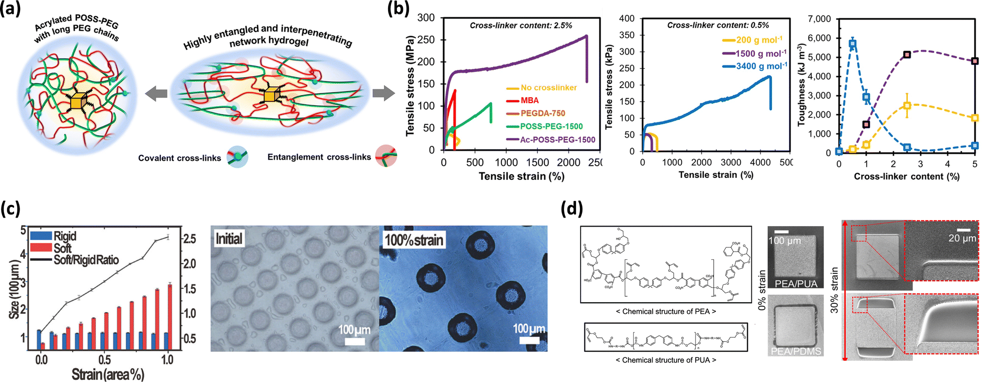 | ||
| Fig. 3 Enhancement of the mechanical properties of polymeric materials using photo-crosslinkers. (a) Schematic illustration of toughening achieved using the Ac-POSS-PEG crosslinker. (b) Mechanical properties of PAM-Ac-POSS-PEG hydrogels with different molecular weights of PEG.74 Copyright 2023, Springer Nature. (c) The ratio of rigid/soft regions and optical images of the patterned substrate.39 Copyright 2024, Wiley-VCH. (d) Chemical structure of PEA/PUA and the optical image of PEA/PUA and PEA/PDMS substrates.76 Copyright 2024, Springer Nature. | ||
Additionally, crosslinking between polymer plays an important role in energy dissipation. For example, Xu et al. enhanced the mechanical performance of a blend of polypropylene (PP) and maleic anhydride-crosslinked styrene-ethylene-butylene-styrene (mSEBS) through photo-crosslinking.75 The study presented two main energy dissipation mechanisms. First, photo-crosslinking increased the rigidity of mSEBS, enabling the absorption and dissipation of strain through a cold drawing process. The second mechanism occurred at the interface between the PP and the mSEBS. Photo-crosslinking formed chemical bonds between the PP and mSEBS, resulting in strong interfacial bonds between the two phases, leading to effective stress transfer and distribution of external stress. Consequently, the strong interfacial bond significantly enhanced the material's tensile strength and resistance to external impacts.
Park et al. synthesized a photo-crosslinkable polymer based on acrylates that enables the simultaneous formation of rigid and soft regions.39 The polymer was functionalized by grafting additional double bonds onto the acrylate backbone using a urethane reaction, specifically by incorporating 2-isocyanatoethyl acrylate (IEA). Upon exposure to UV light, these double bonds selectively crosslinked, forming rigid islands on the substrate. A significant advantage of this polymer was its ability to create fine rigid islands (7 μm) directly on the substrate using a UV mask, eliminating the need for additional processing steps. The researchers demonstrated that by controlling the crosslinking sites of the photo-crosslinkable polymer, they could achieve a modulus increase of up to 38![[thin space (1/6-em)]](https://www.rsc.org/images/entities/char_2009.gif) 000%, confirming its suitability for use as rigid islands. When the substrate, which includes circular rigid islands (100 μm in diameter) and soft regions (50 μm in diameter), was stretched, only the distance between the rigid islands changed, while their size and shape remained consistent (Fig. 3c). This observation demonstrated the effectiveness of this technique in rigid island formation.
000%, confirming its suitability for use as rigid islands. When the substrate, which includes circular rigid islands (100 μm in diameter) and soft regions (50 μm in diameter), was stretched, only the distance between the rigid islands changed, while their size and shape remained consistent (Fig. 3c). This observation demonstrated the effectiveness of this technique in rigid island formation.
Additionally, Kang et al. successfully established a strong interfacial bond between the rigid and soft regions through simultaneous crosslinking.76 This approach effectively prevented delamination while leveraging the modulus difference between polyepoxy acrylate (PEA) and polyurethane acrylate (PUA) (Fig. 3d). The resulting structure exhibited exceptional durability, capable of withstanding structural defects even at a strain of 50%. The residual acrylate groups in PEA bonded with the acrylate groups in PUA, creating robust interfacial adhesion that integrated the two materials into a cohesive unit.
3.2. Dielectric materials
Stretchable electronics now require organic dielectrics to outperform traditional oxide-based dielectrics. While maintaining a high-dielectric constant and lowering dielectric loss is still essential, the organic dielectric must also form stable interfaces with electronic components and withstand various environmental conditions. These requirements underscore the need for more comprehensive molecular design research to meet the high-performance demands of modern devices. Crosslinking is an effective approach to addressing these challenges.141–143 By restricting the mobility of molecular chains, crosslinking reduces orientation polarization and blocks impurity movement, thereby improving dielectric properties.144 Additionally, it enhances solvent resistance and prevents defects at the semiconductor interface.145,146 Furthermore, the smoother surface created through crosslinking can improve the crystalline morphology of the semiconductor, leading to more reliable device performance.147This chapter will discuss how photo-crosslinking can enhance dielectric properties without complex processes: (i) enhancing dielectric properties through adjusting crosslink density; (ii) achieving uniform dispersion of inorganic oxides within the dielectric; and (iii) improving the interface between dielectrics and semiconductors. Finally, we introduce photo-patterning technique for dielectrics through improved solvent resistance.
 | ||
| Fig. 4 Enhancement of dielectric properties. (a) Schematic illustration of photo-crosslinking in a PVDF-HFP crystalline structure. (b) Transfer characteristics of the C10-DNTT OFETs with FPVDF-HFP.77 Copyright 2020, American Chemical Society. (c) Schematic illustration of the crosslinking between BT-SH and P(VDF-CTFE-DB). (d) Dielectric properties as a function of frequency for BT-SH-c-P(VDF-CTFE-DB). (e) Breakdown strength of BT-SH-c-P(VDF-CTFE-DB) before (left) and after 400% strain (right).79 Copyright 2022, Elsevier. (f) Schematic illustration of photo-crosslinking of ZrTA.80 Copyright 2016, American Chemical Society. | ||
Similarly, Kim et al. demonstrated that increasing the crosslinking density through thiol–ene click reaction improved the dielectric properties of vinyl-addition polynorbornene copolymers (P(NB/VNB)).78 By adjusting the amount of pentaerythritol tetrakis(3-mercaptopropionate) (PETMP), they found that adding up to 3 wt% of the crosslinker enhanced the dielectric properties without causing film defects. The crosslinked P(NB/VNB) films with 3 wt% PETMP (cP(NB/VNB)-3) showed a significant increase in the dielectric constant from 2.25 to 3.39 and breakdown electric field from 2.46 MV cm−1 to 3.27 MV cm−1. Moreover, the cP(NB/VNB)-3 exhibited minimal hysteresis during OFET operation, which was due to the reduction of free volume and charge trapping resulting from the high crosslinking density.
In this context, photo-crosslinking can be employed as an effective method to enhance the interface between nanoparticles and the polymer matrix. For example, Ma et al. functionalized barium titanate nanoparticles with thiol groups (BT-SH) to enable crosslinking with a polymer matrix (P(VDF-CTFE-DB)) (Fig. 4c).79 The resulting thiol–ene reaction formed strong bond between BT-SH and P(VDF-CTFE-DB), which improved nanoparticle dispersion and reduced defects within the polymer. As a result, this process could stabilize the dielectric constant and reduce dielectric loss (Fig. 4d). Notably, the crosslinking improved the breakdown strength from 366.7 MV m−1 to 409.2 MV m−1, because BT-SH acted as traps for charge carrier and a scattering center for electrical stress. Additionally, when the film was stretched by 400%, the breakdown strength further increased to 476.6 MV m−1 (Fig. 4e). This notable improvement was due to the orderly alignment of polymer chains and BT-SH during stretching, which prevented the electrical stress concentration.
Recently, organometallic monomers have been utilized to achieve uniform dispersion of inorganic components within the dielectric. Kim et al. introduced a photo-crosslinkable organic–inorganic hybrid gate dielectric based on zirconium tetraacrylate (ZrTA) (Fig. 4f).80 ZrTA consisted of Zr4+ cations and acrylate anions, where the acrylate groups undergo photo-crosslinking to form high-dielectric constant materials (k = 5.48). This hybrid structure combined the benefits of both organic and inorganic materials, resulting in low leakage current (10−7 A cm−2 at 2 MV cm−1) and excellent surface properties, including a very low roughness (0.449 nm), which promoted favorable semiconductor growth. The crosslinked ZrTA film also showed enhanced hydrophobicity due to its organic acrylate matrix, which minimizes polar surface groups like hydroxyls. This reduction in polar groups helped to reduce charge trapping, leading to more efficient charge carrier transport.
Tousignant et al. fabricated a bilayer dielectric structure by photo-crosslinking a polyvinyl alcohol (PVA) surface (Fig. 5a).163 They used 2,2-dimethyl benzodioxinone terminated polycaprolactone (UV-PCL), which effectively crosslinked with the hydroxyl groups of PVA. The UV-PCL layer acted as a protective coating for PVA, providing moisture resistance (Fig. 5b). The crosslinking occurred only at the interface, preventing a decrease in the number of hydroxyl groups in PVA and allowing the dielectric to maintain a high-dielectric constant of 14.5. Additionally, the crosslinking process created a low-polarity environment at the interface, reducing direct interactions between the hydroxyl groups of PVA and the semiconductor (Fig. 5c). As a result, the performance of single-walled carbon nanotube (sc-SWCNT) thin film transistors (TFTs) improved significantly. Devices with the UV-PCL layer exhibited a four-fold improvement in an average hole mobility of 2.8 cm2 V−1 s−1 compared to devices using PVA alone. Furthermore, the UV-PCL dielectric increased the on/off current ratio by ten times, leading to a marked improvement in overall device performance.
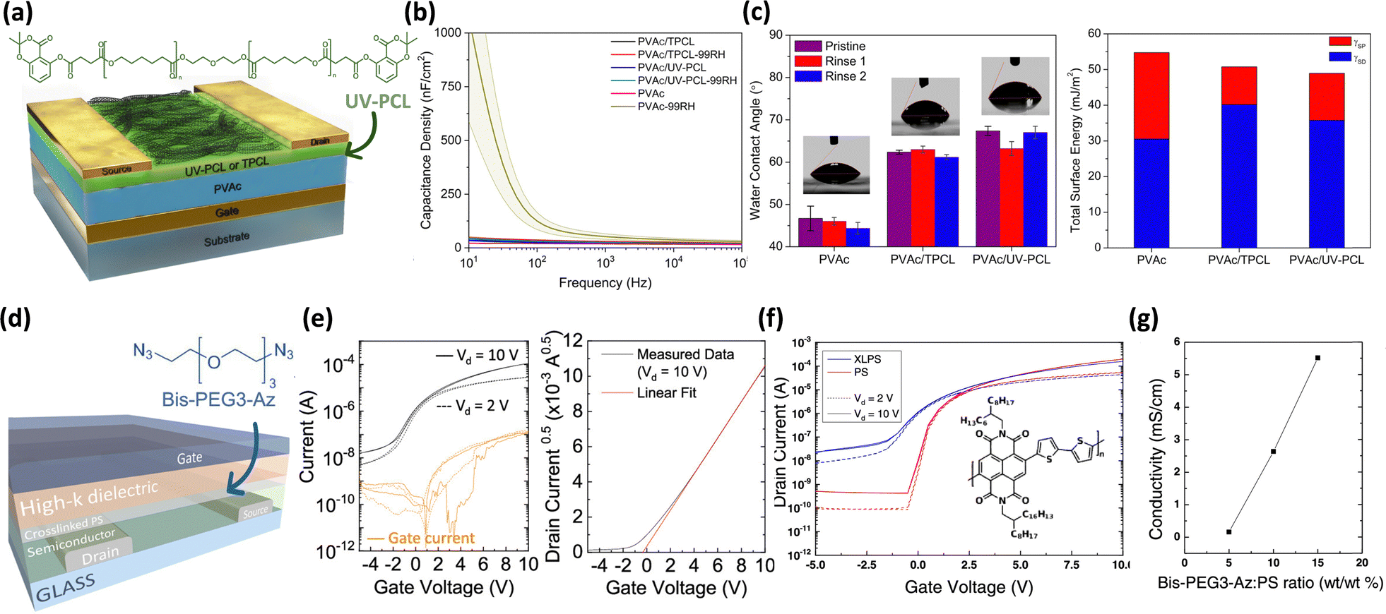 | ||
| Fig. 5 Improvement of the organic semiconductor/dielectric interface through low-permittivity dielectric crosslinking. (a) Schematic illustration of the TFT with a PVAc/UV-PCL dielectric. (b) Moisture-dependent capacitance density of PVAc and PVAc/UV-PCL. (c) Water contact angle and total surface energy for PVAc, and PVAc/UV-PCL.163 Copyright 2023, American Chemical Society. (d) Schematic illustration of the TFT with a CEP/XLPS dielectric. (e) Transfer curve of the OFET based on the CEP/XLPS dielectric. (f) Transfer curves of p-type FETs (DPP–TTT) with the CEP/XLPS and CEP/PS dielectric. (g) Conductivity of n-doped P(NDI2OD-T2) films with crosslinking agent concentration.82 Copyright 2023, American Chemical Society. | ||
Perinot et al. reported another bilayer dielectric structure, demonstrating that the device characteristics depend on the crosslinking of the low-permittivity dielectric layer (Fig. 5d).82 The study employed 1,11-diazido-3,6,9-trioxaundecane (Bis-PEG3-Azide) as the crosslinking agent in a photo-crosslinked polystyrene (XLPS) layer. This crosslinked dielectric effectively suppressed charge injection into the interface or bulk of cyanoethylated pullulan (CEP), even under high electric fields. As a result, TFTs achieved optimal operation at gate voltages below 10 V, with leakage currents kept under 1 nA cm−2 (Fig. 5e). A key finding of the study was the role of the azide-based crosslinker in enhancing n-type doping. During the photo-crosslinking process, the UV activation of azide groups led to the formation of amines, which acted as electron donors. These amines contributed additional electrons to the semiconductor, promoting n-type doping and increasing the overall conductivity of the system (Fig. 5f). When using P(NDI2OD-T2) as the active semiconductor, TFTs with higher concentrations of crosslinkers exhibited a clear linear increase in conductivity (Fig. 5g).
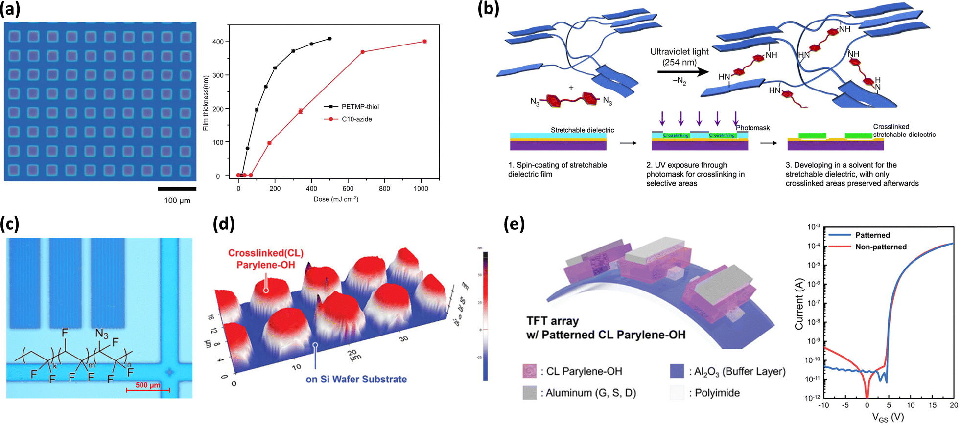 | ||
| Fig. 6 Enhancement of chemical resistance for dielectric micro-patterning. (a) Optical image of photo-patterned NBR and the thickness of NBR patterns in relation to UV exposure doses.123 Copyright 2024, Springer Nature. (b) Photo-patterning process of SEBS using azide-crosslinker.83 Copyright 2018, Springer Nature. (c) Optical image of photo-patterned azide-modified P(VDF-TrFE-CTFE).84 Copyright 2019, American Chemical Society. (d) AFM 3D topology showing the boundaries of the crosslinked parylene-OH (red) on the Si wafer substrate (blue). (e) Schematic structure and transfer curves of the fabricated TFT array using patterned crosslinked (CL) parylene-OH.85 Copyright 2024, Wiley-VCH. | ||
However, the mobility of monomer crosslinkers within dielectrics can negatively impact device performance due to undesired phase separation. As a result, researchers are exploring methods to enhance the chemical resistance of polymer dielectrics without the need for additional crosslinkers, while still enabling photo-patterning.145,167–169 Kallitsis et al. demonstrated that grafting photo-crosslinkable azide groups onto high-k fluoropolymer dielectrics enabled direct patterning through photolithography, resulting in films with very low surface roughness (Fig. 6c).84 More recently, Lee et al. fabricated a hydroxy functionalized parylene thin film (parylene-OH) via chemical vapor deposition achieving intrinsically photo-patterned high-k dielectrics.85 UV irradiation triggered crosslinking, which strengthened the film mechanically while maintaining precise pattern boundaries with a resolution of approximately 5 μm (Fig. 6d). The surface roughness remained unchanged after UV exposure, ensuring stable interfacial properties and enhancing the mobility and current driving performance in IGZO TFT-based semiconductor devices (Fig. 6e)
3.3. Adhesives
In the manufacturing of stretchable electronics, adhesives are needed to meet two different requirements. First, strong adhesion between electronic components is necessary. The adhesive must ensure that components remain securely bonded during the manufacturing process, including solvent treatments and mechanical stresses.170–172 Second, it is important that the device can be easily removed from rigid substrates after fabrication without causing damage.173,174 Stretchable electronics are often fabricated on a rigid supporting substrate; consequently, a method to reduce adhesion strength at a specific stage is necessary. To meet these requirements, adhesive control technologies based on photo-crosslinking have emerged as a promising solution. These technologies facilitate precise spatial control of adhesion through straightforward light exposure, allowing for easy adjustment of adhesive strength.This chapter will explore strategies for (i) improving adhesion strength and (ii) detachment techniques using photo-crosslinking.
 | ||
| Fig. 7 Enhancement of adhesion strength. (a) Schematic illustration of enhancing surface wetting based on temperature and UV irradiation.89 Copyright 2016, American Chemical Society. (b) Peel strength for soft and stiff segments.33 Copyright 2024, Elsevier. | ||
Second, researchers have explored spatial control of adhesive strength through strategic material design. By increasing bending stiffness in specific areas via crosslinking, detachment resistance can be enhanced.175,176 This approach integrates rigid and flexible sections sequentially using photo-patterning, further improving adhesive properties in stretchable devices.90 Lee et al. offered detailed insights into a large-scale bridging mechanism that increased maximum peel strength (Fig. 7b).33 When a rigid area was encountered, a significant portion of the peel force converts into bending energy, which diminished the force propagating interfacial cracks and effectively prevented their propagation. The rigid area redistributed the force, increasing the area available for crack formation, thereby enhancing peel resistance. To maximize debonding resistance, the length of the rigid segments should match the saturation size of the bridging area. For a heterogeneous adhesive with segment lengths of 10 mm, the debonding resistance measured 642.8 N m−1, approximately 13 times higher than that of a fully ductile adhesive. As the length of the rigid segments increased, the debonding resistance rose to 818.8 N m−1 at 14 mm, exceeding that of a fully rigid adhesive.
Photo-crosslinking offers a simpler solution for effective detachment. Increasing crosslink density typically induces volumetric shrinkage due to internal stress, which enhances detachment at the interface. Many researchers have already utilized photo-crosslinking technology in adhesives to enhance detachment performance.191–194 For example, Kim et al. highlighted the ease of detachment in the manufacturing process of ultrathin devices through the formation of an interpenetrating network (IPN).91 After UV exposure, the polyurethane acrylate crosslinker formed an interpenetrating network (IPN), reducing adhesion to less than 1%. This structure allowed for the easy separation of a 1.4 μm ultrathin PET film patterned with silver nanowires (AgNW) and graphene from a thick carrier substrate. This reduction in adhesion ensured that the film remained undamaged during detachment, providing high reliability and yield in the production of ultrathin devices (Fig. 8a).
 | ||
| Fig. 8 Adhesion control for safe detachment. (a) Sheet resistance of the AgNW electrode and the I–V characteristics of graphene.91 Copyright 2019, Royal Society of Chemistry. (b) Peel strength in relation to the crosslinking site ratio and UV irradiation time.195 Copyright 2022, Royal Society of Chemistry. (c) Strategies for the selective removal of adhesion through UV irradiation. (d) Evaluation of peel strength, conversion, and gel fraction changes in UV-debondable adhesive with 3 mol% benzophenone content in relation to UV exposure doses. (e) MD simulated illustration of adhesive delamination post-UV irradiation.92 Copyright 2024, Wiley-VCH. | ||
Similarly, Hwang et al. developed a photo-crosslinkable adhesive by grafting photosensitive side chains through the ring-opening reaction of N-methacryloyl-2-methylaziridine (MAMAz).195 This adhesive demonstrated a reduction in adhesion by up to 99.2% after UV crosslinking, allowing for the non-destructive separation of devices. The detachment performance improved as the amount of crosslinkable side chains increased and as the curing time progressed. Once a certain threshold was reached, the adhesion strength stabilized, with no further reduction (Fig. 8b).
Recent studies have also focused on incorporating photo-initiating groups into adhesive polymers. Kim et al. developed an optically clear adhesive (OCA) by integrating benzophenone derivatives into the polymer network, allowing for easy removal without residue from foldable displays (Fig. 8c).92 Benzophenone exhibited low reactivity under visible light, allowing it to be safely used as a monomer in visible light-induced polymerization. In contrast, it facilitated additional crosslinking through UV-induced reactions. After UV exposure at 4200 mJ cm−2, the OCA containing 3 mol% benzophenone showed a sharp decrease in adhesion from 2.44 N cm−1 to 0.14 N cm−1 (Fig. 8d). Furthermore, the researchers demonstrated through simulations that the increased chain connectivity from crosslinking hindered deformation in the UV-exposed OCA (Fig. 8e). This led to stress concentration at the interface between the OCA and the substrate, enabling easy detachment without residue.
4. Photo-crosslinkable semiconducting polymers for stretchable electronics
Semiconducting polymers have garnered significant attention as promising materials for stretchable electronics due to their inherent mechanical flexibility, tunable properties, solution processability, and cost-effectiveness.196–199 Despite their theoretical advantages, however, these materials often present a trade-off between key advantages and limitations, such as electrical performance versus mechanical durability,200–202 and solution processability versus chemical vulnerability.203–205 Efforts to increase crystallinity for enhanced electrical conductivity often result in brittle mechanical properties. Similarly, while good solubility in organic solvents aids in processing, it also compromises solvent resistance, thereby limiting the applicability of semiconducting polymers in multilayer tandem structures for integrated circuits, sensor arrays, and display fabrication.Photo-crosslinkable semiconducting polymers offer a promising solution to these challenges by simultaneously improving mechanical robustness, stretchability and processibility. First, photo-crosslinking allows facile solution process by selectively imparting the chemical robustness of the material through light-induced chemical bonds. Traditional patterning methods often involve complicated steps with harsh conditions which might degrade the composing materials, including the use of high temperature, sacrificial layers, orthogonal solvents and inkjet printing. In contrast, photo-crosslinking provides a simpler and more efficient strategy for fabricating advanced stretchable organic electronic devices. Second, photo-crosslinking can easily enhance the mechanical durability of semiconducting polymers. A key advantage of photo-crosslinking is its ability to modulate the mechanical properties of semiconducting polymers, addressing the inherent trade-off between electrical performance and stretchability. By chemically linking amorphous and flexible polymer segments, photo-crosslinking can effectively enhance mechanical toughness while maintaining electronic function. Wang et al. revealed that tuning the crystallinity of the crosslinker affects the morphology of the polymer, which in turn influences both its mechanical and electrical properties.206 Through precise control of crosslinking density, the polymer network can be tailored to exhibit both high elasticity and durability under mechanical strain, which is essential for wearable applications. Third, photo-crosslinking enables the functionalization of semiconducting polymers through covalent bonding with functional moieties,127,207,208 imparting desired properties such as enhanced adhesion, passivation, and interfacial compatibility, further improving device reliability and integration.
This section outlines three strategies for rendering semiconducting polymers photo-crosslinkable: (i) molecular engineering of semiconducting polymers by attaching photo-crosslinkable units to the polymer backbone or side chains; (ii) the use of photo-crosslinkable additives that bind directly to the polymer; and (iii) the addition of photo-crosslinkable additives that form covalent bonds exclusively among themselves, without interacting with the semiconductor. Finally, a few research studies to functionalize the surface of semiconductor thin films applying this photo-crosslinking strategy will be discussed
4.1. Molecular design strategies for photo-crosslinking semiconductors
This section will focus on recently reported photo-crosslinkable semiconducting polymers used in OFET applications, following recent reviews of molecular design strategies for crosslinkable conjugated molecules. The incorporation of photo-cleavable or reactive groups into the polymer backbone93 or side chains94,96,98,209 has proven to be a highly effective strategy for patterning semiconducting polymers.203–205,210,211 This approach eliminates the need for additives, which can lead to phase separation and negatively affect the uniformity, morphology, and electrical performance of the material. Various photo-crosslinkable groups, such as azide,96,212 vinyl,213,214 alkyne,215 and oxetane216,217 can be integrated through molecular engineering. Among these, the azide group is particularly favored due to its simplicity and effectiveness of photo-crosslinking. Upon UV light exposure, azide groups form reactive nitrene species and release nitrogen gas. Nitrene species can readily insert into C–H bonds, allowing them to cross-link various sites. Gao et al. utilized this approach by incorporating the azide group into the branching alkyl side chains of a diketopyrrolopyrrole (DPP)-based conjugated polymer, PDPP4T-N3 (Fig. 9b).94 This polymer enabled patterning using facile lithographic techniques, as shown in Fig. 9a. Efficient patterning was achieved using a photomask, because selective UV treatment significantly reduced solubility, allowing for precise patterning. After UV exposure, the unexposed area was removed by soaking in chloroform, resulting in uniform thin films with a thickness of 40 nm and feature sizes as small as 5 μm (Fig. 9c). These patterned films exhibited consistent performance, with average charge mobility of 0.61 ± 0.10 cm2 V−1 s−1. Similarly, Kim et al. synthesized polythiophene (P3HT) with azide groups partially attached to the end of the alkyl chain.96 Even with just 10–20% incorporation of azide units, successful photo-crosslinking was achieved, producing an insoluble semiconducting polymer thin film. They also demonstrated thin film transistors on flexible substrates. This crosslinking method also enhanced the thermal stability of bulk-heterojunction organic photovoltaics (BHJ OPVs) by acting as an in situ compatibilizer at the P3HT/PCBM interface, suppressing macrophase separation. | ||
| Fig. 9 Molecular design strategies for photo-crosslinking semiconductors. (a) Schematic of the photo-patterning procedure using molecular design strategies. (b) Chemical structure of semiconducting photoresist PDPP4T-N3 and its crosslinking mechanism. (c) Optical and AFM images after the photo-patterning process.94 Copyright 2022, Wiley-VCH. (d) Chemical structure of PN3. (e) Optical and AFM images after the photo-patterning process and schematic of device structures.98 Copyright 2024, Wiley-VCH. | ||
The backbone design strategy offers an alternative strategy to side chain modification for introducing reactive groups into a semiconducting polymer backbone. For example, Nyayachavadi et al. developed a DPP-based polymer with 1,3-butadiyne- containing conjugation breaker spacers (CBSs) in the backbone.93 Upon UV irradiation, these butadiyne CBS units underwent polymerization, forming polydiacetylene crosslinks. The crosslinked polymers exhibited improved mechanical properties, such as increased rigidity and thin film stability, while maintaining a solid-state morphology. However, OFET devices using these crosslinked thin films showed a decrease in charge mobility, from 0.058 to 0.013 cm2 V−1 s−1 at best, indicating that crosslinking affected charge transport.
Additionally, the modified polymers can be blended with other conjugated polymers (CPs), serving as the conjugated photo-crosslinker. For example, Xue et al. introduced a new conjugated polymer-based photo-crosslinker, PN3, designed for efficient patterning in OFET applications.98 PN3 features a conjugated backbone made of DPP and bithiophene units, with phenyl-substituted azide groups on its side chains (Fig. 9d). Under UV light, these azide groups crosslink with the alkyl side chains of CP, enhancing the material's solvent resistance. The π–π interactions between PN3 and CP ensure better miscibility, resulting in higher patterning resolution, lower UV exposure doses, and improved sensitivity compared to small molecule-based crosslinkers. PN3 enabled the creation of well-defined patterns with resolutions down to 500 nm, and its doped patterned arrays were used as source-drain electrodes, maintaining excellent charge transport properties (Fig. 9e).
These strategies selectively enhance solvent resistance, enabling efficient photo-patterning and offering significant potential for organic flexible electronics processed through all-photolithography techniques.
4.2. Direct crosslinking via functional additives
Photo-crosslinkable additives are compounds that contain photo-reactive groups, typically located at the ends of their molecular structures. Direct crosslinking refers to a photo-crosslinker creating strong covalent bonds with a CP under UV irradiation, providing significant robustness with minimal additive usage. Unlike methods that modify a polymer's side chains or backbones, this approach allows for more flexible molecular designs, facilitating functionalization without imposing significant synthetic constraints. To maintain effective charge transport, it is essential that additives do not disrupt the polymer's chain packing and aggregation.124,206 Therefore, careful design of their interaction with the CP is crucial.A widely used photo-crosslinkable group is FPA.51,77,218–220 FPAs are favored for their high reactivity and ability to minimize unwanted nitrene attacks on the π-conjugated core, which could otherwise degrade the semiconductor's properties.221 Research has focused on optimizing the performance of FPAs through variations in azide density and chain linkages. For instance, Kim et al. enhanced crosslinking density by using a crosslinker containing four FPAs, facilitating the creation of fully photo-patterned electronics.125 Tan et al. further showed that specific FPAs could achieve unity quantum efficiency for crosslinking, primarily targeting C–H bonds and minimizing side reactions.219
Zheng et al. demonstrated a molecular design using FPA-based crosslinker additives to achieve stretchable, solvent-resistant, and photo-patternable semiconducting polymers using a covalently embedded in situ rubber matrix (iRUM) as shown in Fig. 10a.124 The iRUM system employs an azide-based crosslinker called a BA crosslinker, particularly FPA end-capped polybutadiene, which undergoes both self-crosslinking through azide/C![[double bond, length as m-dash]](https://www.rsc.org/images/entities/char_e001.gif) C cycloaddition and selective crosslinking with a CP via azide/C–H insertion. The researchers systemically compared the impact of crosslinking with the CP and self-crosslinking (Fig. 10b). The researchers revealed that crosslinking with a CP significantly improved patternability but disrupted the aggregation of the CP. On the other hand, self-crosslinking significantly improved chain packing and morphology. Interestingly, both types of crosslinking improved softness and stretchability of the CP by connecting with a long soft chain. Because of dual usage of crosslinking with a specific ratio, determined by different reactivities, BA crosslinkers could facilitate a high charge mobility of 1 cm2 V−1 s−1, stretchability, and chemical robustness for the fabricated multilayer device with the all-solution process (Fig. 10c).
C cycloaddition and selective crosslinking with a CP via azide/C–H insertion. The researchers systemically compared the impact of crosslinking with the CP and self-crosslinking (Fig. 10b). The researchers revealed that crosslinking with a CP significantly improved patternability but disrupted the aggregation of the CP. On the other hand, self-crosslinking significantly improved chain packing and morphology. Interestingly, both types of crosslinking improved softness and stretchability of the CP by connecting with a long soft chain. Because of dual usage of crosslinking with a specific ratio, determined by different reactivities, BA crosslinkers could facilitate a high charge mobility of 1 cm2 V−1 s−1, stretchability, and chemical robustness for the fabricated multilayer device with the all-solution process (Fig. 10c).
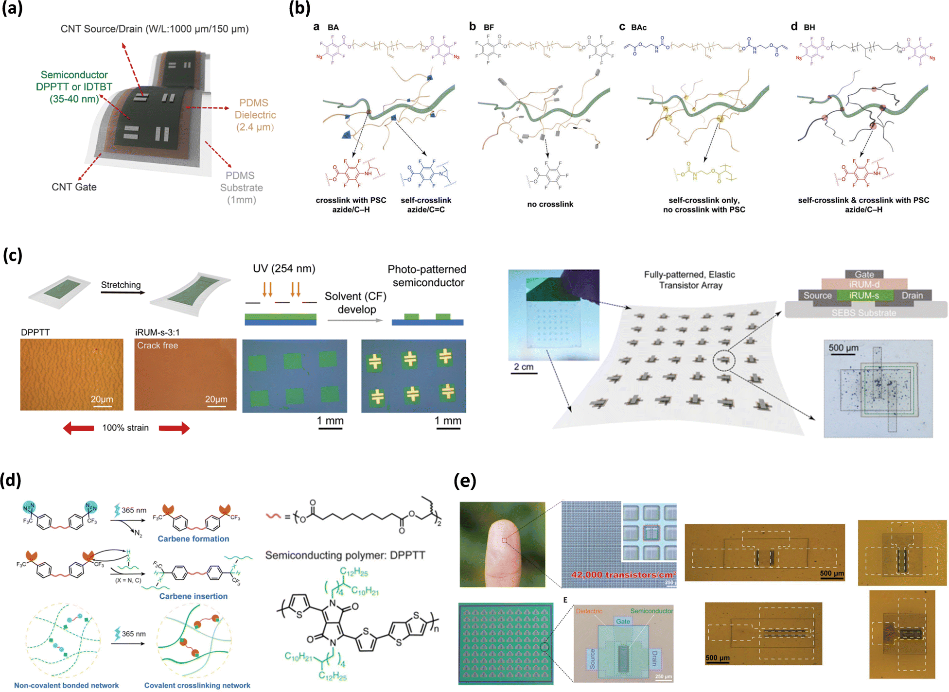 | ||
| Fig. 10 Direct crosslinking via functional additives. (a) Device structure of a fully stretchable transistor using iRUM semiconductors. (b) Chemical structure of the polybutadiene-based precursors for crosslinking with PSC and self-crosslinking. (c) Schematic and optical images of iRUM films during stretching and patterning. Images of the fully patterned, elastic transistor array.124 Copyright 2021, Springer Nature. (d) Mechanism of UV-triggered carbene insertion crosslinking. (e) Images of the elastic transistor array containing 10000 transistors and stretched films.126 Copyright 2021, The American Association for the Advancement of Science. | ||
Another common example of a photo-crosslinkable group is diazirine,222–224 because it transforms into reactive carbene species, reacting specifically to non-conjugated bonds (Fig. 10d) under UV light irradiation, leading to maintaining the electrical properties. For example, Zheng et al. demonstrated a high-resolution, UV-triggered microlithographic process using a trifluoromethyl-substituted diazirine crosslinker to pattern a CP and improve stretchability.126 They introduced a double-end functionalized trifluoromethyl-substituted diazirine crosslinkers with amorphous branched alkyl chains for semiconducting polymer film patterning. The diazirine unit using less than 10 wt% of the diazirine crosslinker was needed to realize 99% film retention and feature sizes down to 4μm were successfully obtained. Finally, they could fabricate high density transistor arrays with 42000 transistors per square centimetre (Fig. 10e). Wu et al. also presented a diazirine-based four-armed crosslinker (4CNN).49 With just 3% 4CNN, p-type, n-type, and ambipolar polymers could be patterned with high precision, achieving feature sizes as small as 5 μm without altering thin film morphology or charge transport properties. This method enabled the fabrication of solution-processable multilayer electronic devices with high device performance and solvent resistance.
4.3. Self-crosslinking networks for enhanced performance
Blending self-crosslinking additives, which form covalent bonds exclusively with themselves under UV irradiation, offers a viable method for fabricating photo-crosslinkable semiconducting thin films. These additives create crosslinked interpenetrating networks that intertwine with a CP, enhancing chemical robustness. However, this approach often requires a higher concentration of additives compared to direct crosslinking, which can lead to severe phase separation. A key advantage of self-crosslinking additives is that they do not disrupt the aggregation of a CP or interfere with the π-conjugated core, thereby maintaining electrical performance. In some cases, they can even promote tighter packing of the polymers, improving electrical performance and charge transport. Additionally, the reduced concern about interactions with the π-conjugated core provide greater flexibility in molecular design, allowing the incorporation of various functionalized materials such as long and elastic components. These materials can achieve both stretchability and patternability simultaneously, making them highly versatile for advanced applications.For example, Tien et al. demonstrated a novel approach of scalable patterning using a thiol–ene reaction (Fig. 11a).97 The process involved blending a high-mobility CP, with elastic rubber like poly(styrene-butadiene-styrene) (SBS). The thiol–ene reaction selectively cross-links the vinyl groups in SBS and a thiol containing additive, trimethylolpropane tris(3-mercapto propionate) (TRIS), creating a semi-interpenetrating polymer network (SIPN) that enhances stretchability and solvent resistance while preserving the electronic properties of the polymer. The thiol–ene approach selectively targets non-conjugated double bonds in SBS, ensuring minimal disturbance to the conjugated polymer's structure. So, the SIPN-based transistors show increased mobilities from 0.61 to 1.18 cm2 V−1 s−1 when applying the strain from 0% to 100% (Fig. 11b). Moreover, the hole mobility could be still maintained after 1000 strain-and-release cycles under a strain of 25%.
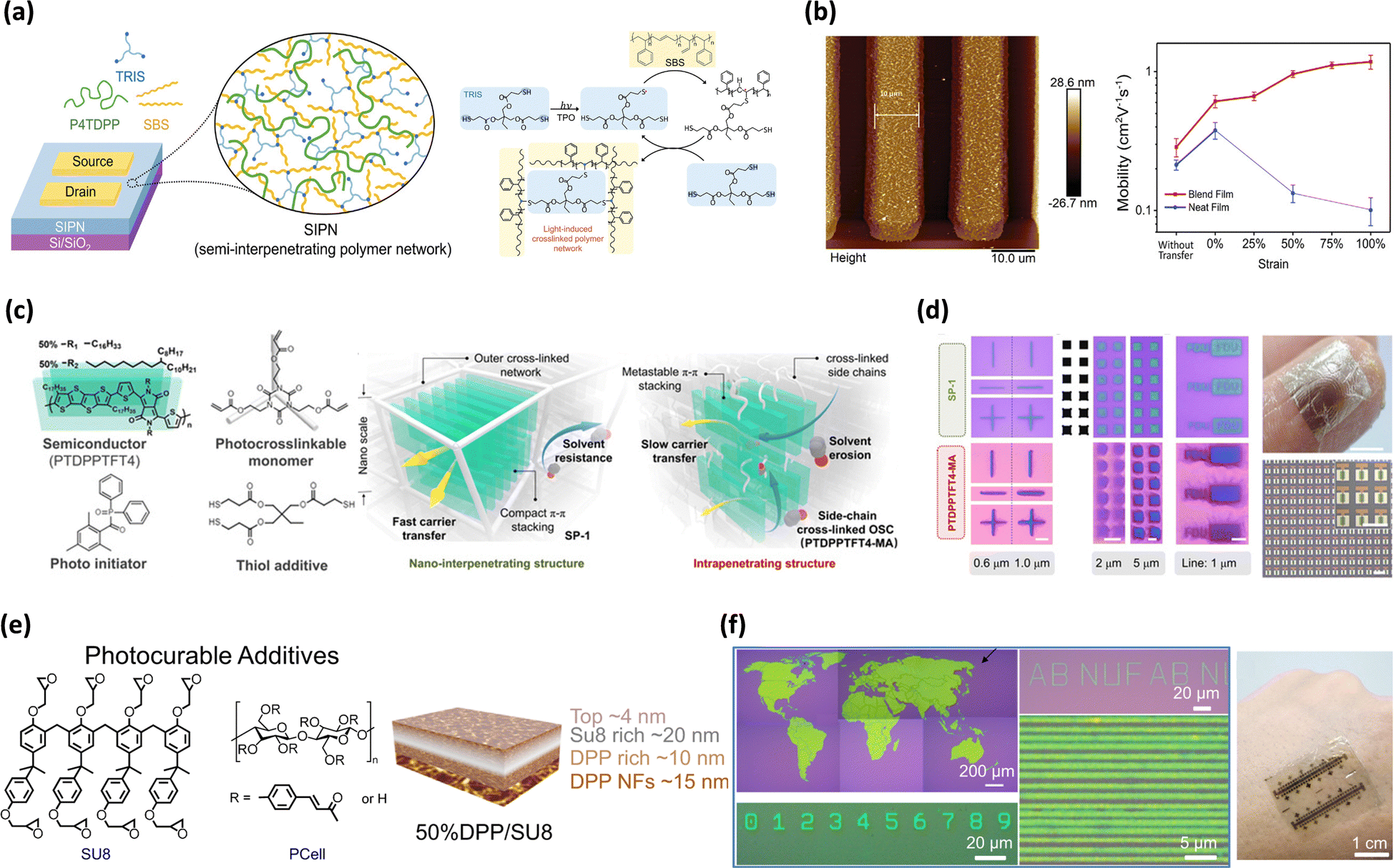 | ||
| Fig. 11 Self-crosslinking networks for enhanced performance. (a) Chemical structure and illustration of a semi-interpenetrating polymer network. (b) AFM image of a photo-patterned semiconducting polymer and mobilities under strain.97 Copyright 2023, Wiley-VCH. (c) Chemical structure of and the schematic diagram of photo-crosslinking of SP-1. (d) Images of patterned SP-1 and transistor arrays.99 Copyright 2021, The American Association for the Advancement of Science. (e) Chemical structure of photocurable additives and schematic of vertical phase separation in 50%DPP/SU8. (f) Images of photo-patterned flexible 50%DPP/SU8.100 Copyright 2021, Springer Nature. | ||
Chen et al. introduced a novel semiconducting photoresist (SP-1) with a nano-interpenetrating structure, designed for all-photolithography processes (Fig. 11c).99 SP-1 consists of a DPP-based CP, acrylate-based crosslinkable monomers with a small amount of photoinitiator and thiol additives. Under UV irradiation, arylate undergoes a radical polymerization reaction, forming a stable interpenetrating network. This allowed for submicrometer patterning with high-density OTFT arrays of 1.1 × 10⁵ units cm−2 (Fig. 11d) while retaining a high charge mobility of 1.11 cm2 V−1 s−1, even after photolithography solution processes. They also demonstrated flexible OFET arrays with a high density OTFT array of 4489 units cm−2 and a mobility of 0.471 cm2 V−1 s−1, achieving 90.8% mobility retention after 1000 bending cycles, making SP-1 a promising material for advanced organic electronics.
Wang et al. presented a wafer-scale, foundry-compatible approach for fabricating polymeric semiconducting layers with 0.5 μm resolution using a three-step photolithographic process (Fig. 11f).100 The CPs such as DPP-based p-type and n-type N2200, were blended with photo-crosslinkable additives like SU-8 and PCell. The patterned layers are chemically inert to aggressive aqueous and organic solvents and thereby withstand subsequent deposition and patterning of the additional organic layers and/or metal contacts used in the circuitry fabrication. These blends exhibited vertical phase separation and a nanofiber morphology, confirmed via AFM, ToF-SIMS, and GIWAXS (Fig. 11e). The resulting OTFTs maintained a high carrier mobility (0.1–0.24 cm2 V−1 s−1) with an improved thermal stability of 175 °C, a mechanical durability of 5000 bending cycles at a radius of 1 mm, and efficient switching performance of subthreshold swing to be 1.4 V dec−1.
4.4. Functional additives for advanced applications
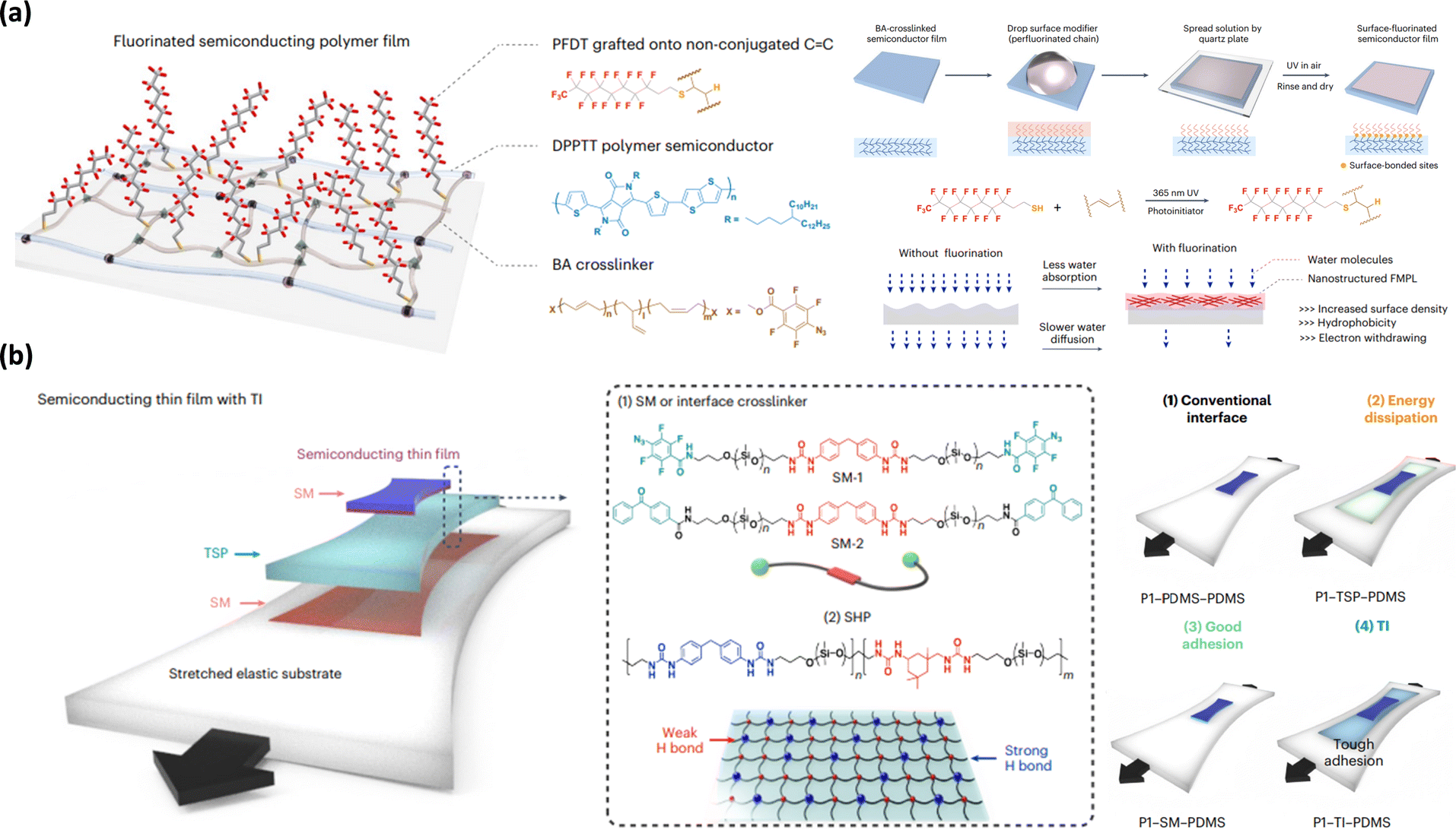
Recently, a few research studies have explored utilizing crosslinkers to impart specialized functions to semiconducting layers, such as surface protection, self-healing, and enhanced interfacial adhesion. When activated by UV irradiation, these functional additives can significantly improve the performance and stability of semiconducting polymer thin films.For example, Zheng et al. proposed a novel approach of covalent functionalization to form a molecular protection layer (Fig. 12a).127 Using a butadiene-azide (BA) crosslinker, the researcher introduced non-conjugated CC bonds as surface reactive sites in a CP. By drop casting perfluorodecanethiol molecules onto the surface of the CP and applying UV irradiation, they induced a thiol–ene reaction that tethered fluoroalkyl chains onto the surface, creating a molecular protection layer. This functionalized surface exhibited hydrophobic properties, preventing water absorption and diffusion, thus maintaining a stable electrical performance of ∼1 cm2 V−1 s−1 in the CP. The fluorinated protection layer outperformed traditional micrometer-thick stretchable polymer encapsulants, showing exceptional stability in harsh environments such as 85–90% humidity for 56 days, and in water or artificial sweat for 42 days.
 | ||
| Fig. 12 Functional additives for advanced applications. (a) Schematic of the process of PSC surface fluorination with photo-crosslinking and the mechanism of achieving long-term environmental stability.127 Copyright 2023, Springer Nature. (b) Schematic of a TI between a semiconducting film and an elastic substrate and schematic of semiconducting thin film on an elastic PDMS substrate with various interface conditions.207 Copyright 2022, Springer Nature. | ||
Additionally, Kang et al. demonstrated an interface engineering strategy (Fig. 12b) to enhance the stretchability of brittle semiconducting polymer thin films.207 They introduced a tough interface (TI) bond, composed of a tough self-healing polymer (TSP) layer and a surface modifier (SM) layer. The TSP, consisting of a 90% self-healing polymer (SHP) and a 10% SM, acted as an energy-dissipating matrix. The SM, based on an FPA crosslinker with a dynamic hydrogen bond and a flexible PDMS backbone, covalently bonded with both the substrate and the semiconducting film under UV irradiation. This interface engineering improved the stretchability of the films from 30% to 110% and enhanced their durability and robustness. It also prevented delamination and delayed crack formation, significantly improving performance in all-polymeric transistor devices.
5. Photo-crosslinking strategy of conductors for stretchable electronics
Intrinsically stretchable conductors are essential components of stretchable electronics, serving as stretchable electrodes and interconnects essential for optimal device performance.225–227 Traditional rigid metal interconnects, while conductive, often fail due to mechanical mismatches, leading to delamination and performance degradation. The stretchable electrodes that are studied a lot are largely divided into three categories: conductive polymers, liquid metals and composites of elastomer and conductive fillers. These limitations have driven the development of photo-patternable conductors, where in situ photo-crosslinking enables precise patterning without the need for complex fabrication processes.23,24,228,229 Conventional thermal and lithographic methods, however, are unsuitable due to the low thermal stability and solvent resistance of stretchable conductors. Photo-patternable conductors, achieved by a material-based molecular design approach provide an alternative, enabling patterning without complex fabrication methods through in situ photo-crosslinking. Such precisely patterned stretchable conductors play a crucial role in the miniaturization of wearable electronics by providing mechanically stable and highly flexible interconnects.This section will explore two major approaches: (i) photo-patterning strategies for CPs and liquid metals, and (ii) 3D-printable nanocomposite-based conductors with various fillers, leveraging from the in situ polymerization. These photo-crosslinkable strategies simplify the fabrication of stretchable, high-performance conductors for flexible electronic applications.
5.1. Photo-crosslinking strategy of stretchable conductors
Some CPs, like poly(3,4-ethylenedioxythiophene):poly styrene sulfonate (PEDOT:PSS),230–232 polyaniline (PANI)233 and polypyrrole234,235 are inherently ductile and conductive due to their energy-band structure.15 These properties make them ideal candidates for use as stretchable conductors in applications such as electrodes and interconnects in flexible electronic devices. However, one of the primary challenges with these materials has been achieving high-resolution patterning for advanced applications. To address these challenges, PEDOT has been the focus of extensive studies aimed at modifying its chemical structure to enhance its chemical resistance during photo-patterning processes. Efforts such as incorporating photo-crosslinkable groups in the side chain of PEDOT have been explored, albeit with trade-offs such as relatively lower conductivity and pattern resolution.104,236–238 Recent advancements have shown that a rational design of photo-crosslinkable PEDOT additives can significantly improve conductivity while enabling precise patterning.For example, Zheng et al. employed a rationally designed monolithic optical microlithographic process to fabricate stretchable and patternable conductors by precisely optimizing the chemical structure of PEDOT.126 In this approach, the conductive PEDOT polymer formed a double-network structure with a polyethylene glycol dimethacrylate (PEGDMA) crosslinker. The strong interaction between PEDOT and PEG linker initiated a microstructural transition in PEDOT from a core–shell structure to a more extended form, thus forming the first conductive network. Upon UV exposure, PEGDMA underwent radical polymerization, creating a secondary network around the entangled PEDOT chains, which enables high-resolution patterning down to 2 μm feature. This technique allowed PEDOT to achieve improved conductivity, reaching up to 52.5 kS m−1 after methanol treatment, along with enhanced stretchability. The resulting structure exhibits increased solubility modulation and structural stability, making it well-suited for flexible electronics.
Furthermore, Jiang et al. introduced a topological supramolecular network using polyrotaxane (PR) structures to further improve the stretchability and conductivity of PEDOT films (Fig. 13a).103 This strategy relied on the hypothesis that topological molecular design can decouple competing properties from multiple molecular building blocks, enabling high conductivity, stretchability and patternability in one system (Fig. 13b). The PR-PEGMA additive, composed of a PEG backbone with sliding cyclodextrins (CDs) functionalized with PEG methacrylate (PEGMA) side chains, prevented PEG crystallization, thereby avoiding phase separation and enhancing stretchability of PEDOT. The PR-PEGMA enhanced PEDOT aggregation by replacing the insulating PSS, boosting conductivity to 2700 S cm−2 after sulfuric acid treatment while maintaining stretchability up to 150% strain. The acid treatment further enhanced PEDOT's crystallinity, forming interconnected fibers that substantially improved conductivity without compromising mechanical flexibility. The molecular engineering approach facilitated charge transport through PEG's role in promoting PEDOT aggregation, while the sliding CDs prevent phase separation, ensuring a uniform material distribution.
 | ||
| Fig. 13 Photo-crosslinking strategy of stretchable conductors. (a) Chemical structure of PR-PEGMA and illustration of the interaction between PR and PEDOT:PSS for enhanced conductivity. (b) Image showing conformal interface and conductivity over strain plots showing high conductivity versus previously reported PEDOT:PSS.103 Copyright 2022, The American Association for the Advancement of Science. (c) Synthesis route and chemical structure of stretchable and patternable grafted copolymers. (d) Stress–strain curve showing the mechanical properties and images showing patternability. (e) I2 vapor doping method description and subsequent resistivity.106 Copyright 2019, Royal Society of Chemistry. (f) Schematic of modified LMP stock solution preparation and patterned LM image. (g) Schematic during stretching process.35 Copyright 2024, Wiley-VCH. | ||
Another effective strategy for enhancing the electrical conductivity of CPs while maintaining their suitability for flexible applications is chemical doping.98,105,239 This approach plays a significant role in converting these polymers into highly conductive materials by increasing their charge carrier density and facilitating efficient charge transport. Chemical doping can be utilized to create photo-crosslinkable and stretchable conductors, which are valuable in stretchable electronics and bioelectronics. For example, Wang et al. introduced a multifunctional graft copolymer that combines a conductive P3HT backbone with poly(PEGMMA-co-GMA) side chains (Fig. 13c).106 The P3HT backbone provides electrical conductivity due to its conjugated structure, allowing for efficient charge transport. The poly(PEGMMA-co-GMA) side chains added mechanical stretchability and hydrophilicity, while the glycidyl methacrylate (GMA) segments enabled photo-crosslinking (Fig. 13d). Chemical doping with iodine vapor increased the electrical conductivity to 21.5 S m−1, making the material suitable for conductors in stretchable electronics and bioelectronics, retaining conductivity even under deformation and after patterning (Fig. 13e).
Liquid metals, such as eutectic gallium–indium (EGaIn), have recently gained significant attention as highly conductive and stretchable materials due to their exceptional deformability.240–243 These properties make them promising candidates for use in advanced flexible electronics. However, the inherent challenges with EGaIn—such as its fluidity, extremely high surface tension, and the rapid formation of an oxide layer—complicate its integration as interconnects or direct contact pads in electronic devices. Recent research has focused on overcoming these limitations by utilizing liquid metal particles (LMPs), enabling precise patterning for stretchable electronic applications. For example, Lee et al. introduced a novel method for large-area patterning of EGaIn using a conventional photolithographic process.244 In this approach, the EGaIn particles were encapsulated with PSS, which enhances their mechanical and chemical stability. This encapsulation allowed for uniform thin film coating improving the overall processability of the material. By using dimethyl sulfoxide (DMSO) as a lift-off solvent, the cohesion between the EGaIn particles was increased, enabling a metal-level conductivity of 2.2 × 10⁶ S m−1 without requiring an activation step. This technique enabled high-resolution patterning down to 10 μm and supports multilayered fabrication of stretchable electronics.
Similarly, Wu et al. introduced stretchable liquid metal pattern fabrication using a chemically functionalized EGaIn particle ink in combination with polymer precursors.35 The EGaIn particles were chemically modified with a 2-hydroxyethyl acrylate (2-HEA) ligand, which facilitates strong covalent bonds during the photo-polymerization process (Fig. 13f). Upon exposure to UV light, 2-HEA acted as a polymer precursor, creating a crosslinked network with the modified LMPs with high resolution around 20 μm. Subsequent mechanical sintering broke the oxide barriers between the LMPs, further enhancing their electrical conductivity of 3 × 10⁶ S m−1. When the material was stretched, the poly(HEA) layer, enriched with hydroxyl groups, enables a natural oxide-driven interface reconciliation of the EGaIn particles, which further boosted the stretchability of the material to up to 2500% strain (Fig. 13g).
These innovations in molecular design and crosslinking strategies represent significant advancements in creating stretchable, high-conductivity materials for use in bioelectronic applications, marking a critical step forward in the development of flexible electronic devices.
5.2. Nanocomposite-based conductors for stretchable electronics
Nanocomposite-based conductors, consisting of conductive fillers embedded in an elastomer matrix, present a promising alternative to conventional electronic materials, owing to their enhanced electrical conductivity and mechanical flexibility.225,245–248 When combined with fast photo-reactive monomers like acrylates, these composites with CNTs,249–252 silver nanowires,253–255 graphene oxide256,257 or ionic liquids258,259 can be utilized as photo-patternable conductors. Upon exposure to UV light, a percolated network of conductive fillers forms within the elastomer matrix, enabling continuous charge transport even under mechanical deformation, creating flexible pathways for carrier movement. For example, Yi et al. developed a technique to fabricate high-resolution conductive films and micropatterns using an acylate based photoresist and reduced graphene oxide (RGO) with UV photolithography (Fig. 14a).107 In this method, RGO was formed through in situ photoreduction of graphene oxide (GO) in photoresist/GO solution, achieving conductivities of up to 9.90 S cm−1 for films and 0.98 S cm−1 for micropatterns. The photoinitiator XBPO played a crucial role, initiating both the polymerization of photoresists and the reduction of GO, leading to well-dispersed photoresist/RGO (PRGO) and preventing its oxidation. This approach created patterns with a precision of about 30 μm, compatible with various substrates like PET and silicon.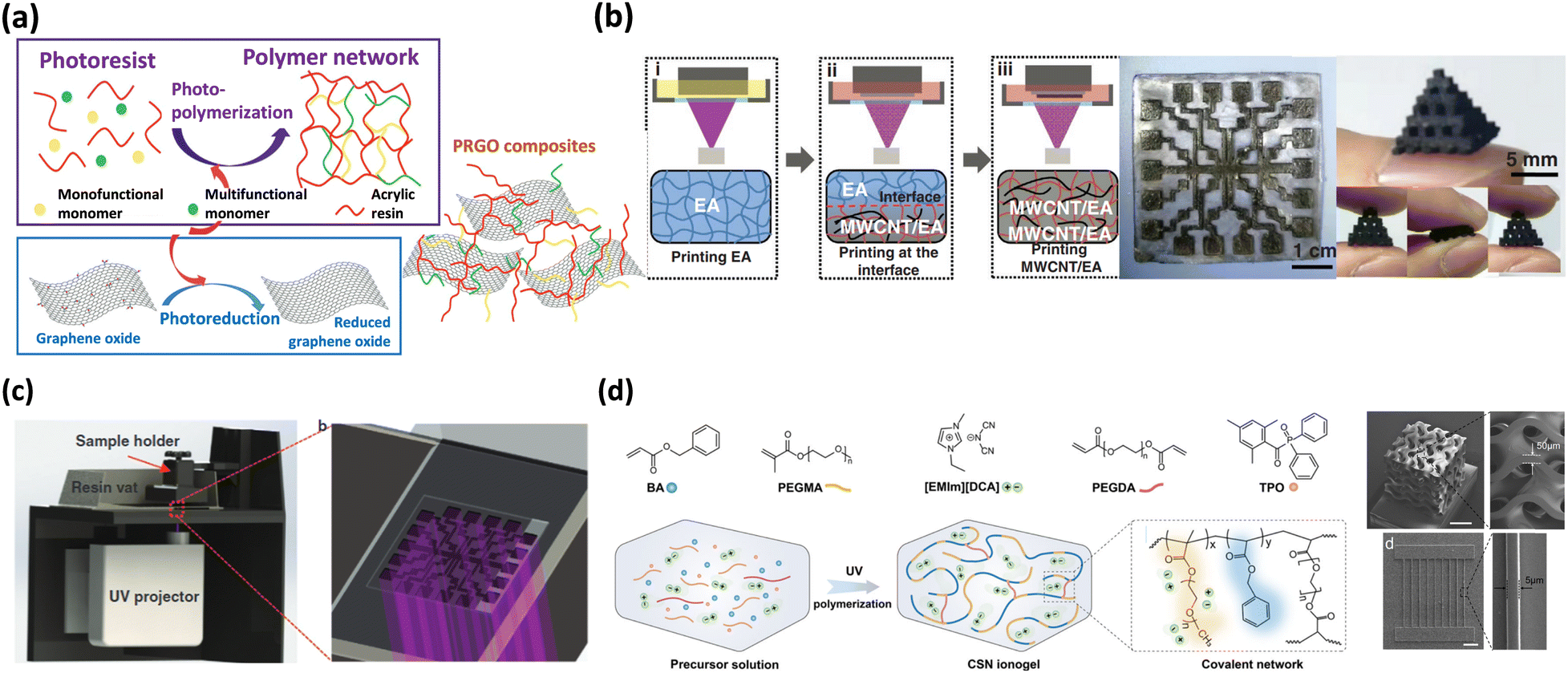 | ||
| Fig. 14 Nanocomposite-based conductors for stretchable electronics. (a) Schematic illustration of the formation of photoresist/RGO composites through in situ photoreduction.107 Copyright 2023, Wiley-VCH. (b) Schematic showing the 3D printing process of a 4 × 4 strain sensor array and its image. (c) Diagram of the DLP-based 3D printer.108 Copyright 2021, Wiley-VCH. (d) Chemical structures and photo-polymerization process to prepare a CSN ionogel and SEM images of a 3D printed ionogel.109 Copyright 2024, Springer Nature. | ||
Benefiting from in situ photo-crosslinking, high-resolution photo-crosslinkable conductors with excellent mechanical and electrical properties can be rapidly formed, extending beyond traditional 2D conductive electrodes. These conductors create precise percolated networks of conductive fillers, ensuring stable conductivity even under strain. This method greatly improves the scalability, speed, and cost-effectiveness of producing flexible electronics like sensors and smart devices. Additionally, the ability to integrate multiple materials into a single structure enhances design versatility, enabling the development of advanced applications, including flexible capacitive sensors, force sensors, and 4D-printed devices with expanded functionality.
Xiao et al. showcased the use of digital light processing (DLP) 3D printing to pattern multiwalled carbon nanotubes (MWCNTs) in a UV-curable elastomer matrix (Fig. 14b and c).108 This method allowed for precise and scalable fabrication of complex MWCNT patterns, improving the sensitivity and functionality of strain sensors. With 2 wt% MWCNTs, the sensors achieved a high sensitivity of 8.939, a broad strain detection range of 0.01% to 60%, and exceptional durability over 10000 cycles. This technique is ideal for flexible, high-performance IoT devices, including human motion detectors and distributed strain sensors.
He et al. developed conductive nanostructured ionogels (CSNs) for 3D-printed capacitive sensors, which exhibit a high ionic conductivity of 3 S m−1, an extreme stretchability of 1500%, a low hysteresis of 0.4%, and excellent thermal stability (Fig. 14d).109 These ionogels were prepared by inducing microphase separation via photo-polymerization using acrylate-based monomers and ionic liquids, creating conductive nanochannels intertwined with a crosslinked polymer framework. The use of ionic liquids like [EMIm][DCA] enhanced electrical double layer formation, increasing capacitance and sensitivity up to 15.1 kPa−1. The high printability of CSN ionogels enabled complex geometries to improve sensor performance, making them ideal for wearable and soft electronics.
Similarly, Yu et al.110 and He et al.34 introduced innovative 3D printable nanocomposite ionogels using photo-crosslinkable acrylate-based monomers. Yu et al. developed a one-step photopolymerized ionogel incorporating Al(OH)3 nanoparticles as multifunctional crosslinking sites, featuring a high stretchability of 487% and a strength of 2.72 MPa. He et al. demonstrated DLP-based multimaterial 3D printing using UV-curable ionic conductive elastomers (UV-ICEs), achieving a high stretchability of 1300% and complex designs for capacitive sensors and 4D printing applications.
6. Applications
In the previous sections, we systematically examined the role of photo-crosslinking at the component level, detailing its impact on mechanical robustness, chemical resistance, and electrical stability. However, beyond the optimization of individual components, it is crucial to understand how these fundamental crosslinking strategies translate into practical benefits at the device level. By leveraging the advantages established at the material level, photo-crosslinking provides a pathway toward the scalable and reliable fabrication of fully integrated flexible and stretchable applications.37,196,260 The key benefits of photo-crosslinking in integrated devices can be categorized into three main aspects: (i) precise patterning, (ii) simplified fabrication and (iii) enhanced interfacial stability. First, photo-crosslinking enables precise patterning of organic materials,261 allowing for the incorporation of complex geometric designs with finely tuned mechanical properties.39 This capability is particularly beneficial for optimizing the sensitivity, stability, and selectivity of flexible and stretchable sensors. Additionally, by adjusting the degree of crosslinking, it is possible to modulate the material's modulus, which is essential for maintaining mechanical compliance in stretchable applications.262 Second, photo-crosslinking simplifies and optimizes device fabrication by reducing reliance on traditional multi-step photolithography processes that require photoresists. Conventional fabrication methods necessitate careful control of solvent orthogonality to prevent film swelling or material diffusion during curing, which can lead to pattern inaccuracies and resolution limitations. In contrast, photo-crosslinking enables direct solution-based processing, allowing the fabrication of large-area devices with minimized defects.263 Third, photo-crosslinking enhances interfacial stability between multiple electronic layers, ensuring robust adhesion and mechanical durability. Repeated processing steps in conventional methods can degrade thin films, posing challenges for reliable device integration. Photo-crosslinking improves the chemical resistance of organic layers by facilitating both lamination and patterning in a controlled manner, making them solvent-resistant and mechanically stable under deformation.This section will focus on fully integrated flexible and stretchable devices utilizing photo-crosslinkable components. We will explore three major application categories: (i) physical sensors, which leverage changes in capacitance or material properties enabled by crosslinking, (ii) OFETs, the foundational circuits in organic electronics, and (iii) OSCs, where crosslinking ensures high efficiency and stability. Each category will highlight how photo-crosslinking contributes to both enhanced device performance and reliability.
6.1. Physical sensors
Stretchable physical sensors capable of measuring external stimuli in real time are essential components of E-skins, which play a critical role in applications such as soft robotics and skin-attachable healthcare devices.264 Physical sensors, such as pressure and strain sensors, can be classified based on their transduction mechanisms, where mechanical deformation is detected through piezoresistive, capacitive, piezoelectric, or triboelectric methods. Ideal sensors should meet essential criteria, including high sensitivity, stable linearity, low hysteresis, and rapid response times. Unlike conventional rigid sensors, stretchable sensors utilizing elastic polymers as a matrix can withstand deformation while maintaining their electrical properties, thereby enhancing sensing accuracy and improving signal-to-noise (S/N) ratios under optimal conditions.265–267 However, the elastic characteristics of the polymer matrix can lead to decreased linearity, low repeatability, and diminished durability in practical applications. Recent studies have demonstrated that crosslinking is an effective method for addressing these challenges, and this strategy can be applied to all components of the sensors, including the active layer and electrodes.The photo-crosslinking approach is applicable to both structure-based40 and material-based111–113 strategies for fabricating active layers in stretchable tactile sensors. The structure-based approach, which involves geometric microengineering of the active layer into structures like micropyramids,114,115,268 improves sensor performance parameters such as sensitivity, response time, relaxation time, and detection limit. A key advantage of photo-crosslinking in this context is its ability to precisely modulate material properties, making it an effective tool for optimizing sensor performance through a structure-based strategy. For example, Park et al. developed capacitive strain-insensitive pressure sensors by synthesizing a photo-crosslinkable polymer based on acrylates.39 The soft acrylate polymer enabled the selective formation of highly crosslinked rigid islands, exhibiting a 38000% increase in modulus upon UV irradiation. The rigid region remains mechanically robust while the surrounding soft matrix preserved stretching durability under strain. By incorporating these rigid islands as the dielectric layer in a capacitor, they successfully fabricated a strain-insensitive pressure sensor (Fig. 3c).
Su et al. reported a wearable pyramidal-shaped, photo-patternable pressure sensor array integrated with a wearable measurement unit (Fig. 15a).40 They employed a PDMS matrix with a benzophenone photoinitiator and observed an increase in viscosity as the system photo-crosslinked under UV light. The blended solution was cast onto a 3D-printed plastic mold, which was subsequently spun during photo-patterning under a photomask to create a thin shell pyramidal structure (Fig. 15b). By leveraging photo-crosslinking, they were able to efficiently fabricate this structure, which enhanced interfacial capacitive transduction and ultimately resulted in superior sensing performance. Consequently, the pressure sensor array exhibited remarkable sensing properties, with a maximum sensitivity of 104 kPa−1, and demonstrated excellent repeatability, maintaining stable operation under 4 kPa for 1500 cycles.
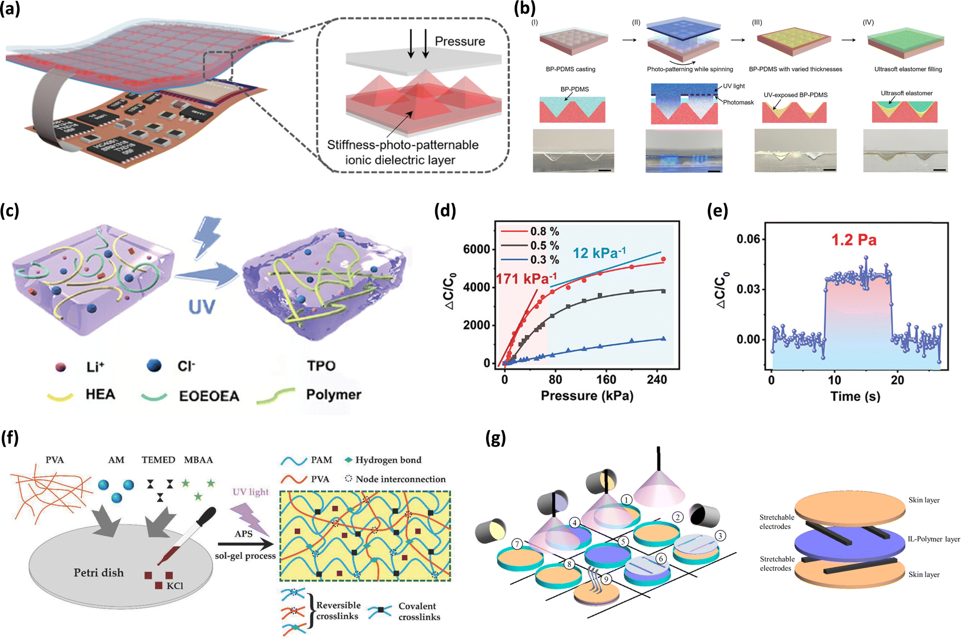 | ||
| Fig. 15 Schematic diagram of the application of photo-crosslinked polymers in physical sensors. (a) Schematic illustration of a photo-patterned pressure sensor array. (b) Schematic illustration of the fabrication process and corresponding photographs. Scale bars, 2 mm.40 Copyright 2022, American Chemical Society. (c) Schematic illustration of synthesis of the photocurable ionic hydrogel. (d) Relative capacitance variation as a function of ionic liquid concentration. (e) Relative capacitance variation when a limit of detection pressure is applied to the device.111 Copyright 2023, Wiley-VCH. (f) Schematic illustration of synthetic process for binary networked hydrogel.119 Copyright 2018, Wiley-VCH. (g) Schematic illustration of the sensor fabrication process and architecture.121 Copyright 2017, IOP-Publishing. | ||
In a material-based approach, various elastic materials can be used as candidates for the active layer, including viscoelastic elastomers and ionic conductive hydrogels.116–118 In the first approach, researchers usually fabricate sensors by incorporating conductive fillers such as CNTs, silver nanowires into stretchable substrates such as polyurethane (PU) and PDMS. Certain photo-crosslinked viscoelastic polymers exhibit excellent cyclic durability, thermal stability, and chemical resilience, along with a low Young's modulus, making them suitable for attachment to human tissue. Due to the reduced glass transition temperature, crosslinked elastomers are deformable and resistant to fracture at room temperature, resulting in increased mechanical strength. The second approach involves ionic conductive hydrogels, which consist of biocompatible hydrophilic polymer gels combined with salts.88,269,270 These ionic conductors facilitate ion transport, sharing the same electrical signal carriers with biological systems, thus making them suitable for real-time health monitoring. Similar to the structural approach, crosslinking methods are frequently employed to enhance cyclic durability and stability.
Guo et al. presented ionic conductive hydrogels fabricated through the photo-crosslinking of monomer blend solution, which incorporates 2-HEA as a crosslinker, along with the 2-(2-ethoxyethoxy)ethyl acrylate (EOEOEA) monomer and lithium chloride (Fig. 15c).111 The ionic liquid provides a source of ions, increasing the carrier concentration and the ion transport rate, which subsequently enhances the electrical conductivity of the material. Notably, sensitivity increased with higher concentrations of lithium chloride, with an optimal ion concentration of 0.8% required to preserve the hydrogel's transparency (Fig. 15d). Utilizing this pressure sensor, a minimal detectable pressure of 1.2 Pa was achieved, along with a sensitivity of 171 kPa−1 for pressures ranging from 0 to 60 kPa (Fig. 15e).
Similarly, Ge et al. developed a conductive dual-crosslinked hydrogel composed of PVA and polyacrylamide (PAM) through a sol–gel process using photo-crosslinking.119 This process involved the use of PVA, acrylamide (AM), the chemical crosslinker N,N′-methylenebisacrylamide (MBAA), potassium chloride, and N,N,N′,N′-tetramethylethylenediamine (TEMED) as ionic materials to enhance the reaction rate and conductivity. In addition to the covalently crosslinked PVA polymer matrix, the in situ crosslinked PVA long chains formed dynamic, reversible crosslinks that further increase the flexibility of the network (Fig. 15f). This was achieved through sliding and unwrapping between the polymer chains, which facilitates energy dissipation. The resultant network exhibited notable piezoresistive behavior, characterized by a high sensitivity (0.05 kPa−1 for pressures ranging from 0 to 3.27 kPa), rapid response times, and exceptional stability for pressure sensor applications.
Zhang et al. presented a 3D-printable dual-crosslinked ionogel strain sensor characterized by high stretchability, self-healability, and self-adhesiveness.113 They incorporated a multi-armed, vinyl-functionalized crosslinker, VPOSS, into a polymer matrix comprising the ionic liquid EMIM(EtO)2PO2 to facilitate efficient photo-crosslinking of polyacrylic acid (PAA). The PAA side chains induced physical crosslinking, which is sacrificial to the external strain. This dual-crosslinked ionogel exhibited remarkable stretchability and durability, demonstrating mechanical properties such as the absence of fatigue resistance and the ability to maintain performance at extreme temperatures (150 °C and −60 °C). The ionic liquid served to weaken the interactions between the polymer molecular chains, thereby enhancing the stretchability of the network, which contributes to a linear relationship between strain and electrical resistance (ΔR/R0).
Despite the significant potential of hydrogel-based materials for stretchable tactile sensors, current fabrication methods, such as mold curing, limit their applicability in stretchable devices. To address this challenge, some researchers have employed 3D printing technologies to construct intricate microstructures.120 Lee et al. developed piezoelectric sensors using 3D-printable, photocurable materials.121 Specifically, they utilized an ionic conductive hydrogel composed of acrylate-based monomer, 2-[[(butylamino)carbonyl]oxy]ethyl acrylate (BACOEA) and the ionic liquid 1-ethyl-3-methyl-imidazolium tetrafluoroborate (EMIMBF4), combined with the acrylate-based crosslinker, glyceryl propoxy triacrylate (GPTA). This mixture was cast into a rigid PTFE Petri dish and subsequently cured. For the substrate, TangoPlus, a rubber suitable for 3D printing, was molded on both sides of the composite, while MWCNTs were employed as electrodes (Fig. 15g). The sensor demonstrated a linear relationship between electrical resistance and strain (<30%) under a force of 15 N.
Similarly, Yan et al. developed an ionic conductive tactile sensor with high printability using DLP 3D printing technology.112 They blended acrylamide (AA) and AM monomers with magnesium chloride and incorporated polyethylene glycol diacrylate (PEGDA) as a crosslinker, curing the material layer by layer to create complex structures. The hydrogel was constructed using a bottom-up printing approach, and the sensor exhibited a high sensitivity (0.06 kPa−1) across a broad detection range (26 kPa–70 kPa) and exceptional stability, sustaining 200 cycles of pressure loading.
To develop fully elastic electronic devices, it is essential to create organic electrodes that conform to biological tissues and accommodate body movements. Several methods have been explored to enhance the elasticity of rigid conductive materials, including application of metallic thin films through structural engineering,271,272 incorporation of conductive nanoparticles and nanowires into elastomers,273–275 and fabrication of intrinsically elastic electrodes.276 Among these strategies, the crosslinking method offers an effective approach for developing intrinsically stretchable organic electrodes while maintaining high conductivity by using brittle materials such as PEDOT:PSS. Although PEDOT exhibits high electrical conductivity and oxidation resistance, its intrinsic stretchability is limited to less than 10%, which hinders its application in wearable electronics. Wang et al. developed an elastic capacitive strain sensor using stretchable PEDOT:PSS electrode through the thermal crosslinking of PSS chains with poly(ethylene glycol) diglycidyl ether (PEGDE) as a crosslinker via esterification, resulting in a high-quality capacitance strain sensor electrode.122 Wang et al. fabricated a strain sensor device with stretchable PEDOT:PSS electrodes positioned at both ends of the PVDF-HFP active layer. Contrast to the uncrosslinked PEDOT:PSS electrodes, crosslinked PEDOT:PSS electrodes showed low hysteresis under 50% strain and linear relationship between the capacitance variation and strain under 50%, indicating excellent sensing performance. Also, the sensor exhibited stable electrical performance after 2000 cycles.
6.2. OFETs
The simplicity of patterning offered by photo-crosslinkable elastomers,32 as explained for the above physical sensors, also provides significant advantages for OFETs. This advancement is particularly noteworthy as it simplifies conventional photoresist-based fabrication processes, enhancing the resolution of transistor array patterns. Furthermore, the reduction in complex processing steps minimizes the risk of damage to dielectric277 or semiconducting layers,99 reducing current leakage and improving overall transistor performance.77,278 Photo-crosslinking between layers also helps prevent layer delamination, ensuring stable device operation. The improved stability enables the development of reliable electronic devices with complex circuits.123,279–282 Assigning photo-crosslinkable characteristics to essential components, such as the gate dielectric283–286 and the semiconductor layer functioning as the active matrix,51,99,204 ensures effective circuit array isolation, further enhancing the reliability of the entire device. Consequently, recent research has increasingly focused on developing OFET arrays through all-solution processes and all-photolithography, highlighting the streamlined and efficient approach that photo-crosslinkable organic materials offer for next-generation device fabrication. Moreover, the self-healing properties95 and improved interfacial adhesion207,208 in thin film layers make photo-crosslinkers advantageous for developing stretchable devices. The application of photo-crosslinkers will likely play a critical role in enhancing the resolution of OTFTs and in the production of integrated flexible and stretchable devices in the future.Using photo-crosslinkable organic materials in OFETs, Kim et al. introduced a versatile three-dimensional crosslinker, 4Bx, with a tetrahedral geometry containing four photo-crosslinkable azide moieties.125 When mixed with solution-processable materials, 4Bx enables photo-patterning of all layers, including polymer semiconductors, polymer insulators, and metal nanoparticles. While crosslinkers typically reduce the intrinsic crystallinity of semiconductors, leading to decreased electrical performance, 4Bx is highly effective even at low concentrations (as little as 1 wt% in the semiconductor layer). Its azide groups enable the formation of a photo-crosslinked network, providing strong solvent resistance without significantly compromising performance. Fig. 16a shows the fabrication of all-photo-patterned OFETs and logic circuits on a flexible plastic substrate, using materials such as the PEN elastomer and AgNPs for the substrate and electrodes. The dielectric and organic semiconducting layers were made flexible by employing PMMA and P(DPP2DT-TVT), respectively. The average hole mobility was estimated to be 0.81 ± 0.18 cm2V−1 s−1. It is noteworthy that a maximum mobility of 1.03 cm2 V−1 s−1 was obtained even though all electronic components were photo-patterned. Fig. 16b shows an optical image of a functional logic gate fabricated using this process, with a 4Bx crosslinker incorporated into the n-type semiconductor to enable photo-patterning.
 | ||
| Fig. 16 Schematic diagram of application of photo crosslinked polymers in OFETs. (a) Schematic drawing and photographic image of all-photo-patterned OTFTs and logic circuits fabricated on a plastic substrate by patterning of the semiconducting channel, gate dielectric, and electrode materials. (b) Optical images and schematic circuit diagrams of NOT, NAND, and NOR logic gates based on all-photo-patterned p-type and n-type OTFTs.125 Copyright 2020, Springer Nature. (c) Schematic illustrating the central role of intrinsically stretchable transistors and circuits for e-skin applications and the high-performance requirements (left). Photo image and schematic of an active-matrix sensor array (right). (d) Photography of the display system and intrinsically stretchable transistor array under deformed/released and corresponding LED display images.123 Copyright 2024, Springer Nature. (e) Schematics representing the formation of photo-patterns and the corresponding network structure through a thiol–ene click reaction between the polymer ionogels and the crosslinker in an ionic liquid (left). Schematic of an ionogel block after self-healing, and a twisted self-healed ionogel (right).87 Copyright 2023, Elsevier. | ||
In the study reported by Zheng et al., direct optical polymer patterning was used to fabricate high-density monolithic elastic circuits.126 The researchers developed an optical microlithography technology by incorporating a branched-diazirine crosslinker into a semiconductor polymer, enabling precise photo-crosslinking. This approach controlled the local solubility of the polymer, allowing the fabrication of micrometer-scale transistors with excellent uniformity and high yield. With the mechanism of the PhotoAssist strategy, based on UV-triggered crosslinking, they facilitated the production of an elastic transistor array comprising 10000 transistors, which could seamlessly attach to the skin. A 10 × 10 transistor array, fabricated using the same strategy, demonstrated ideal p-type transfer characteristics with minimal hysteresis and an average saturation mobility of 0.255 cm2 V−1 s−1. Furthermore, the array withstood 100% strain both parallel and perpendicular to the charge transport direction without showing any visible cracks or delamination and electrical performance degradation.
Zhong et al. conducted systematic research on each thin film layer to develop high-density, intrinsically stretchable transistors and integrated circuits with high driving ability, fast operation speed, and large-scale integration.123 Their intrinsically stretchable transistors demonstrated an impressive average field-effect mobility of over 20 cm2 V−1 s−1 under 100% strain, with a device density of 100000 transistors cm−2 (Fig. 16c). The performance was enhanced by incorporating crosslinkable moieties into the dielectric, semiconductor, and electrode layers. Notably, the dielectric layer was photo-patterned through a straightforward thiol–ene reaction using a high-κ elastic dielectric material, nitrile-butadiene rubber (NBR) with CC bonds, and a thiol-containing crosslinker. This study demonstrated the fabrication of high-density, intrinsically stretchable transistors by employing different materials and patterning methods for each layer. These transistors were further used to build several applications, including intrinsically stretchable pseudo-CMOS inverters, active-matrix tactile sensor arrays, and LED displays driven by intrinsically stretchable transistors (Fig. 16d). The work highlighted the potential of photo-crosslinking strategies and material innovations in advancing next-generation stretchable electronic devices.
Furthermore, flexible and stretchable OFETs hold significant potential for bioelectronic applications.287,288 Jiang et al. focused on developing an ideal interface for seamless and biocompatible integration with the human body.103 Their research led to two key biomedical innovations, which are a soft and stretchable electrode array capable of stable electrophysiological monitoring of deformable tissues and a stretchable high-density array that enables localized neuromodulation for precise control of individual muscle activities. These advancements demonstrated the potential of stretchable OFETs to bridge electronics and biology, paving the way for high-performance, adaptable biomedical devices designed for dynamic interaction with living tissues. Photo-crosslinking offers not only the advantage of creating high-resolution patterns but also introducing self-healing properties. In the recent paper of Kim et al., 3D polymer networks based on a thiol–ene click reaction were used to fabricate self-healing ionogels, which serve as high-capacitance gate dielectrics for OTFTs.87 The resulting ionogels exhibited self-healing capability under mild conditions of 60 °C for 3 minutes. Fig. 16e illustrates the formation of a crosslinked network via UV-induced disulfide bonds, allowing for both photo-patternability and self-healing, as demonstrated by the disulfide metathesis reaction.
6.3. OSCs
Due to environmental concerns and fossil fuel depletion, OSCs have gained significant research interest.289,290 The photoelectric conversion process in OSCs begins with the photoexcitation in the photoactive layer, where photon absorption generates excitons. These excitons diffuse to the donor–acceptor (D–A) interface and dissociate into holes and electrons, rapidly transferred to the electrodes. Through photo-crosslinking, the thermodynamically metastable state can be preserved, ensuring the morphology of the photoactive layer remains stable under external stimuli, which is essential for advanced OSC applications.36,101,291,292 Leveraging the stabilizing effect of photo-crosslinking, researchers have applied this strategy in various studies, such as constructing stable BHJs in the active layer and substituting fullerene acceptors with non-fullerene alternatives.For the practical application of stretchable OSCs, an increase in power conversion efficiency (PCE) resulting from the stabilized morphology of the BHJ in the active layer, along with robust mechanical properties under external strain, is essential. However, high-efficiency OSCs typically require extended π-conjugated backbone molecules and highly ordered crystallinity, which can reduce the device's stretchability. To address the challenge of balancing mechanical and optoelectronic performance in OSCs, many researchers are employing crosslinking reactions in the side chains and main backbone to stabilize both morphology and device performance. Ma et al. highlighted the thermal stability benefits provided by the crosslinker DTODF-4F with the BHJ active layer.293 This crosslinker with a conjugated fluorene-based backbone and epoxy side chains formed a stable network structure through in situ crosslinking under UV radiation, which enhances exciton dissociation and reduces traps and defects, leading to improved PCE. While BHJ films are typically optimized through thermal annealing, they suffer from morphological instability under heating or solar radiation, resulting in phase separation and performance degradation (Fig. 17a). The incorporation of C-DTODF-4F, which is photo-crosslinked DTODF-4F, allowed for thermal annealing-induced optimization, followed by UV radiation to fix the morphology, ensuring stability even under continuous heating. Furthermore, they demonstrated that PCE is more stable with DTODF-4F, maintaining 72.7% of its original value after 50 hours of aging, compared to 27.5% for the device without crosslinker (Fig. 17b). This indicated improved thermal stability due to crosslinking. They also demonstrated that adding 0.5% DTODF-4F reduces trap-assisted recombination, as evidenced by the reduction in the Voc slope from 1.19 kT q−1 to 1.11 kT q−1. After aging, the Voc slope of devices without crosslinker increased from 1.19 to 1.25, while the DTODF-4F-based devices showed a minimal change from 1.11 to 1.13, demonstrating the superior long-term stability of DTODF-4F-based devices (Fig. 17c).
 | ||
| Fig. 17 Schematic diagram of application of photo crosslinked polymers in OSCs. (a) Schematic illustration of the mechanism for crosslinker induced morphological stability. (b) Efficiency evolution of devices w/o and with crosslinker under a thermal condition of 150 °C. (c) Relationship between Voc with the light intensity.293 Copyright 2022, American Chemical Society. (d) Schematic illustration of crosslinked active layer films. (e) Optical image of intrinsically stretchable OSCs and the corresponding device structure. (f) Normalized PCE variation of intrinsically stretchable OSCs as a function of strain and stretching test cycles. (g) Stability of OSCs under thermal aging and light illumination.102 Copyright 2022, Wiley-VCH. | ||
Inspired by the stabilizing effects of photo-crosslinking on OSCs, researchers have explored the substitution of fullerene-based materials with non-fullerene alternatives.294–298 While fullerene acceptors have been widely used in OSCs due to their electron affinity and light absorption, they have limitations such as uncontrollable energy levels and instability. To address these issues, Wang et al. introduced crosslinker small molecules 2,6-bis(4-azidobenzylidene)cyclohexanone (BAC) into the donor polymer PM6 and developed the device with an Y6 acceptor molecule (Fig. 17d).102 Using this active layer, Wang et al. fabricated an intrinsically stretchable OSC device with other all-stretchable device components (Fig. 17e). It is important to note that a high density of direct photo-crosslinking can adversely affect the optoelectronic properties of OSCs due to steric hindrance. Therefore, the incorporation of a small amount of crosslinker was critical, for achieving the optimized fill factor (FF), short-circuit current density (Jsc), and PCE (Fig. 17f). The OSC maintained its photovoltaic performance of 80% PCE under 20% strain and 64% PCE retention after strain-release cycles under 20% strain. Furthermore, in order to ensure long-term device stability, which encompasses the ability to withstand high temperatures and light exposure, crosslinked layers exhibited significantly slower degradation of PCE, even under harsh conditions (Fig. 17g).
7. Conclusion and outlook
This review has explored recent advancements in photo-crosslinking technologies for flexible and stretchable electronics, which offer effective methods for controlling the physical, chemical, electrical, and mechanical properties of materials. We began by discussing how photo-crosslinking strategies have been employed to enhance the performance of essential components—insulators, semiconducting polymers, and conductors—each presenting unique challenges and requirements. We also highlighted the role of these strategies in facilitating the fabrication of integrated stretchable devices.For individual components, insulators require distinct crosslinking approaches depending on their function as substrates, dielectrics, or adhesives. For substrates, improving energy dissipation and controlling chain mobility through photo-crosslinking is crucial for enhancing mechanical durability. In dielectric materials, reducing charge trapping and minimizing defects are key objectives, while for adhesives, photo-crosslinking enables precise control over adhesion strength. In semiconducting polymers, photo-crosslinking enhances mechanical durability, electrical performance, and chemical resistance through three key strategies: molecular design, direct crosslinking, and the development of self-crosslinking networks. We also investigated how these strategies impart additional functionalities, further improving both stability and performance. Finally, in conductors, the functionalization of molecular structures and the incorporation of conductive fillers into photo-crosslinkable polymers enable precise micropatterning and advanced 3D printing, ensuring the integrity of electrical connections even under mechanical deformation.
We further explored how integrated devices benefit from the reliable and facile integration enabled by photo-crosslinking. For example, physical sensors demonstrate excellent durability and conductivity under mechanical stress, with potential applications in 3D printing. In OFETs, photo-crosslinking enhances the resolution of transistor arrays while simplifying the manufacturing process, thereby improving the reliability of high-density integrated devices. Similarly, in OSCs, crosslinked photoactive layers minimize charge traps and defects, ensuring thermodynamic metastability and consistent performance over prolonged operation.
While significant progress has been made in applying photo-crosslinking to stretchable electronics, several considerable challenges remain. For instance, residual small molecules such as photoinitiators and crosslinkers may degrade device electrical properties and adversely affect biocompatibility by causing skin irritation. Additionally, operating conditions in various environments where prolonged exposure to light or high temperatures may trigger additional crosslinking reactions that compromise environmental stability and long-term reliability. Balancing the conflicting demands for flexibility and durability is challenging, and achieving a uniformly controllable crosslinking density remains difficult. Moreover, as device systems become more complex, integrating photo-crosslinkable materials becomes increasingly demanding, requiring careful consideration of adhesion, interfacial compatibility, and process scalability. Overcoming these challenges is essential to fully realize the potential of photo-crosslinkable materials in next-generation flexible and stretchable electronic devices. One promising direction is the precise molecular design of photo-crosslinkable materials, which could unlock advanced functionalities such as self-healing, seamless attachment, molecular passivation, and reversible crosslinking. These innovations are particularly relevant for human body sensors, where they could improve comfort, extend lifespan, and maintain high sensitivity with reliable electrical performance. Additionally, there is great potential in developing advanced applications, such as 3D and 4D printed electronics, where materials can not only offer flexibility and stretchability but also exhibit dynamic, stimuli-responsive behavior, enabling structural and functional transformations over time. By programming crosslinking-induced shape morphing and mechanical adaptability, 4D printing can facilitate the development of reconfigurable and self-adaptive devices with enhanced performance. Such innovations are especially valuable in fields that require both functional complexity and stretchability, including soft robotics and multi-sensor systems.
Beyond fabrication advancements, integrating photo-crosslinking with frontier technologies such as machine learning-driven material design and dynamically reconfigurable devices holds significant promise. Machine learning approaches can facilitate the rapid optimization of crosslinkable material formulations by predicting the relationships between molecular structure, crosslinking density, and final device performance. This data-driven approach could accelerate the discovery of novel crosslinkable systems tailored for specific applications, optimizing mechanical compliance, conductivity, and chemical stability. Furthermore, in dynamically reconfigurable electronics, photo-crosslinking could enable adaptable and reprogrammable materials that respond to external stimuli, such as heat, light, or mechanical strain, paving the way for advanced smart materials with tunable properties. The integration of photo-crosslinking with 4D printing methodologies further expands the possibilities of dynamically changing electronic architectures, enabling multifunctional devices capable of real-time adaptation to environmental conditions.
To fully exploit the potential of photo-crosslinking technology, further research must focus on broadening the range of material functionalities and deepening our understanding of the complex relationships between molecular structure, reactivity, and microphase transitions during the crosslinking process. By optimizing these factors, photo-crosslinking technologies can achieve both precision and functionality, driving new innovations in stretchable electronics. This progress will open up new possibilities across diverse fields, including medical technology, neuroscience, robotics, and environmental monitoring.
Author contributions
J. H. O. proposed the topic of the review and supervised the writing. M. K. and H. P. equally contributed to writing the following main sections: introduction; photo-crosslinkable insulator/semiconductor/conductor for stretchable electronics; and conclusion and outlook. E. K. and M. C. wrote the application section. All authors contributed to the discussion and revision of the manuscript.Data availability
Data sharing is not applicable, since no new data were created or analyzed in this review.Conflicts of interest
There are no conflicts to declare.Acknowledgements
This work was supported by the National Research Foundation of Korea (NRF) grant (2023R1A2C3007715, RS-2024-00398065) through the NRF by the Ministry of Science and ICT (MSIT), Korea. The Institute of Engineering Research at Seoul National University provided research facilities for this work.References
- J. A. Rogers, T. Someya and Y. Huang, Science, 2010, 327, 1603–1607 CrossRef CAS PubMed.
- S. Hou, C. Chen, L. Bai, J. Yu, Y. Cheng and W. Huang, Small, 2024, 20, 2306749 CrossRef CAS PubMed.
- K. K. Kim, Y. Suh and S. H. Ko, Adv. Intell. Syst., 2021, 3, 2000157 CrossRef.
- H. Kim, J. Lee, U. Heo, D. K. Jayashankar, K.-C. Agno, Y. Kim, C. Y. Kim, Y. Oh, S.-H. Byun and B. Choi, Sci. Adv., 2024, 10, eadk5260 CrossRef.
- Q. Zhao, E. Gribkova, Y. Shen, J. Cui, N. Naughton, L. Liu, J. Seo, B. Tong, M. Gazzola and R. Gillette, Sci. Adv., 2024, 10, eadn7202 CrossRef CAS PubMed.
- D. Liu, X. Tian, J. Bai, S. Wang, S. Dai, Y. Wang, Z. Wang and S. Zhang, Nat. Electron., 2024, 7, 1176–1185 CrossRef.
- S. J. Woodman, D. S. Shah, M. Landesberg, A. Agrawala and R. Kramer-Bottiglio, Sci. Robot., 2024, 9, eadn6844 CrossRef PubMed.
- D. Hu, F. Giorgio-Serchi, S. Zhang and Y. Yang, Nat. Mach. Intell., 2023, 5, 261–272 CrossRef.
- Z. Wang and J. Zhu, Small, 2024, 20, 2311012 CrossRef CAS PubMed.
- J. Pu, Q. Cao, Y. Gao, Q. Wang, Z. Geng, L. Cao, F. Bu, N. Yang and C. Guan, Adv. Mater., 2024, 36, 2305812 CrossRef CAS.
- S. Xu, Y. Zhang, J. Cho, J. Lee, X. Huang, L. Jia, J. A. Fan, Y. Su, J. Su and H. Zhang, Nat. Commun., 2013, 4, 1543 Search PubMed.
- S. Naficy, F. Oveissi, B. Patrick, A. Schindeler and F. Dehghani, Adv. Mater. Technol., 2018, 3, 1800137 CrossRef.
- Y. Fu, H. He, Y. Liu, Q. Wang, L. Xing and X. Xue, J. Mater. Chem. C, 2017, 5, 1231–1239 RSC.
- G. Zhou, J.-H. Byun, Y. Oh, B.-M. Jung, H.-J. Cha, D.-G. Seong, M.-K. Um, S. Hyun and T.-W. Chou, ACS Appl. Mater. Interfaces, 2017, 9, 4788–4797 CrossRef CAS PubMed.
- D. C. Kim, H. J. Shim, W. Lee, J. H. Koo and D. H. Kim, Adv. Mater., 2020, 32, 1902743 CrossRef CAS.
- H. Cho, B. Lee, D. Jang, J. Yoon, S. Chung and Y. Hong, Mater. Horiz., 2022, 9, 2053–2075 RSC.
- X. Yang, C. Forró, T. L. Li, Y. Miura, T. J. Zaluska, C.-T. Tsai, S. Kanton, J. P. McQueen, X. Chen and V. Mollo, Nat. Biotechnol., 2024, 42, 1836–1843 Search PubMed.
- J. Gu, Y. Jung, J. Ahn, J. Ahn, J. Choi, B. Kang, Y. Jeong, J.-H. Ha, T. Kim and Y. Jung, Nano Energy, 2024, 130, 110124 CrossRef CAS.
- X. Huang, L. Liu, Y. H. Lin, R. Feng, Y. Shen, Y. Chang and H. Zhao, Sci. Adv., 2023, 9, eadh9799 CrossRef CAS PubMed.
- Y. Li, W. Liu, Y. Deng, W. Hong and H. Yu, npj Flexible Electron., 2021, 5, 3 CrossRef.
- Y. Wang, Q. Liu, J. Zhang, T. Hong, W. Sun, L. Tang, E. Arnold, Z. Suo, W. Hong and Z. Ren, Adv. Mater., 2019, 31, 1902955 CrossRef PubMed.
- H. Gao, Z. Wang, F. Yang, X. Wang, S. Wang, Q. Zhang, X. Liu, Y. Sun, J. Kong and J. Yao, Nat. Commun., 2024, 15, 2321 CrossRef CAS PubMed.
- T. Q. Trung and N. E. Lee, Adv. Mater., 2017, 29, 1603167 CrossRef PubMed.
- Q. Zhang, J. Liang, Y. Huang, H. Chen and R. Ma, Mater. Chem. Front., 2019, 3, 1032–1051 RSC.
- H. Hu, C. Zhang, Y. Ding, F. Chen, Q. Huang and Z. Zheng, Small Methods, 2023, 7, 2300671 CrossRef CAS PubMed.
- G. Balakrishnan, J. Song, C. Mou and C. J. Bettinger, Adv. Mater., 2022, 34, 2106787 CrossRef CAS PubMed.
- Y. Li, N. Li, W. Liu, A. Prominski, S. Kang, Y. Dai, Y. Liu, H. Hu, S. Wai and S. Dai, Nat. Commun., 2023, 14, 4488 CrossRef CAS PubMed.
- S. Chen, L. Sun, X. Zhou, Y. Guo, J. Song, S. Qian, Z. Liu, Q. Guan, E. Meade Jeffries and W. Liu, Nat. Commun., 2020, 11, 1107 CrossRef CAS PubMed.
- Q. Xu, P. McMichael, J. Creagh-Flynn, D. Zhou, Y. Gao, X. Li, X. Wang and W. Wang, ACS Macro Lett., 2018, 7, 509–513 CrossRef CAS.
- Y. Liu, M. Pharr and G. A. Salvatore, ACS Nano, 2017, 11, 9614–9635 CrossRef CAS PubMed.
- Y. Lee, J. W. Chung, G. H. Lee, H. Kang, J.-Y. Kim, C. Bae, H. Yoo, S. Jeong, H. Cho and S.-G. Kang, Sci. Adv., 2021, 7, eabg9180 CrossRef CAS PubMed.
- J. S. Kwon, H. W. Park, D. H. Kim and Y.-J. Kwark, ACS Appl. Mater. Interfaces, 2017, 9, 5366–5374 CrossRef CAS PubMed.
- Q. Li, X. Wan, Z. Xu, Y. He, Q. Xue and C. Yang, Extreme Mech. Lett., 2024, 67, 102128 CrossRef.
- X. He, J. Cheng, Z. Li, H. Ye, X. Wei, H. Li, R. Wang, Y.-F. Zhang, H. Y. Yang and C. Guo, ACS Appl. Mater. Interfaces, 2022, 15, 3455–3466 CrossRef PubMed.
- D. Wu, S. Wu, P. Narongdej, S. Duan, C. Chen, Y. Yan, Z. Liu, W. Hong, I. Frenkel and X. He, Adv. Mater., 2024, 36, 2307632 CrossRef CAS PubMed.
- M. Li, Y. G. Yang, Z. K. Wang, T. Kang, Q. Wang, S. H. Turren-Cruz, X. Y. Gao, C. S. Hsu, L. S. Liao and A. Abate, Adv. Mater., 2019, 31, 1901519 CrossRef PubMed.
- W. Wang, S. Wang, R. Rastak, Y. Ochiai, S. Niu, Y. Jiang, P. K. Arunachala, Y. Zheng, J. Xu, N. Matsuhisa, X. Yan, S. Kwon, M. Miyakawa, Z. Zhang, R. Ning, A. M. Foudeh, Y. Yun, C. Linder, J. B.-H. Tok and Z. Bao, Nat. Electron., 2021, 4, 143–150 CrossRef CAS.
- W. Wang, Y. Jiang, D. Zhong, Z. Zhang, S. Choudhury, J.-C. Lai, H. Gong, S. Niu, X. Yan and Y. Zheng, Science, 2023, 380, 735–742 CrossRef CAS PubMed.
- H. G. Park, M. Kim, H. Park and J. H. Oh, Adv. Funct. Mater., 2024, 34, 2312034 CrossRef CAS.
- Q. Su, C. Liu, T. Xue and Q. Zou, ACS Appl. Mater. Interfaces, 2022, 14, 33641–33649 CrossRef CAS PubMed.
- A. Ribas-Massonis, M. Cicujano, J. Duran, E. Besalú and A. Poater, Polymers, 2022, 14, 2856 CrossRef CAS PubMed.
- K. S. Lim, J. H. Galarraga, X. Cui, G. C. Lindberg, J. A. Burdick and T. B. Woodfield, Chem. Rev., 2020, 120, 10662–10694 CrossRef CAS PubMed.
- M. Körner, O. Prucker and J. Rühe, Macromolecules, 2016, 49, 2438–2447 CrossRef.
- G. Becker, Z. Deng, M. Zober, M. Wagner, K. Lienkamp and F. R. Wurm, Polym. Chem., 2018, 9, 315–326 Search PubMed.
- Q. Liu and J. L. Locklin, ACS Omega, 2020, 5, 9204–9211 CrossRef CAS PubMed.
- Z. Geng, J. J. Shin, Y. Xi and C. J. Hawker, J. Polym. Sci., 2021, 59, 963–1042 CrossRef CAS.
- C. E. Hoyle, A. B. Lowe and C. N. Bowman, Chem. Soc. Rev., 2010, 39, 1355–1387 Search PubMed.
- M. L. Lepage, C. Simhadri, C. Liu, M. Takaffoli, L. Bi, B. Crawford, A. S. Milani and J. E. Wulff, Science, 2019, 366, 875–878 CrossRef CAS PubMed.
- C. Wu, C. Li, X. Yu, L. Chen, C. Gao, X. Zhang, G. Zhang and D. Zhang, Angew. Chem., 2021, 133, 21691–21698 Search PubMed.
- S.-S. Ge, B. Chen, Y.-Y. Wu, Q.-S. Long, Y.-L. Zhao, P.-Y. Wang and S. Yang, RSC Adv., 2018, 8, 29428–29454 RSC.
- S. H. Kim, S. Chung, M. Kim, D. Yoo, E. Ok, S. Kim, K. C. Song, Y. J. Song, B. Kang and K. Cho, Adv. Funct. Mater., 2023, 33, 2212127 CrossRef CAS.
- J. Lee, S. Z. Hassan, S. Lee, H. R. Sim and D. S. Chung, Nat. Commun., 2022, 13, 7021 CrossRef CAS PubMed.
- N. Zivic, P. K. Kuroishi, F. Dumur, D. Gigmes, A. P. Dove and H. Sardon, Angew. Chem., Int. Ed., 2019, 58, 10410–10422 CrossRef CAS PubMed.
- T. Sun, L. Kang, H. Zhao, Y. Zhao and Y. Gu, Adv. Sci., 2024, 11, 2302875 CrossRef CAS PubMed.
- T. Tsuchimura, J. Photopolym. Sci. Technol., 2020, 33, 15–26 CrossRef CAS.
- N. Klikovits, P. Knaack, D. Bomze, I. Krossing and R. Liska, Polym. Chem., 2017, 8, 4414–4421 RSC.
- F. Dumur, Polymers, 2023, 15, 4202 CrossRef CAS PubMed.
- L.-Y. Peng, S.-L. Xiang, J.-D. Huang, Y.-Y. Ren, P. Hong, C. Li, J. Liu and M.-Q. Zhu, Chem. Eng. J., 2024, 482, 148810 CrossRef CAS.
- J. Deng, S. Bailey, S. Jiang and C. K. Ober, J. Am. Chem. Soc., 2022, 144, 19508–19520 CrossRef CAS PubMed.
- Y. Liu, D. Wang, Q. Wang and W. Kang, Small Methods, 2024, 8, 2400112 CrossRef CAS PubMed.
- Y. Liu, D. Wang, H. Wang, H. Chen, Q. Wang and W. Kang, Small, 2025, 2412297 CrossRef PubMed.
- L. Di Terlizzi, A. Martinelli, D. Merli, S. Protti and M. Fagnoni, J. Org. Chem., 2022, 88, 6313–6321 CrossRef PubMed.
- W. Xu, T. Li, G. Li, Y. Wu and T. Miyashita, J. Photochem. Photobiol., A, 2011, 219, 50–57 CrossRef CAS.
- L. Zhang, B. Feng, S. Pang, H. Xin, K. Li and Y. Jin, J. Mol. Struct., 2024, 1304, 137653 CrossRef CAS.
- C. J. Martin, G. Rapenne, T. Nakashima and T. Kawai, J. Photochem. Photobiol., C, 2018, 34, 41–51 CrossRef CAS.
- N. A. Romero and D. A. Nicewicz, Chem. Rev., 2016, 116, 10075–10166 CrossRef CAS PubMed.
- F. Mohamadpour and A. M. Amani, RSC Adv., 2024, 14, 20609–20645 RSC.
- C. K. Prier, D. A. Rankic and D. W. MacMillan, Chem. Rev., 2013, 113, 5322–5363 CrossRef CAS PubMed.
- M. Reckenthaeler and A. G. Griesbeck, Adv. Synth. Catal., 2013, 355, 2727–2744 CrossRef CAS.
- B. R. Pfund and O. S. Wenger, JACS Au, 2025, 5, 426–447 CrossRef CAS PubMed.
- N. Zivic, M. Bouzrati-Zerelli, A. Kermagoret, F. Dumur, J. P. Fouassier, D. Gigmes and J. Lalevée, ChemCatChem, 2016, 8, 1617–1631 CrossRef CAS.
- S. Poplata, A. Tröster, Y.-Q. Zou and T. Bach, Chem. Rev., 2016, 116, 9748–9815 CrossRef CAS PubMed.
- T. Hughes, G. Simon and K. Saito, Mater. Horiz., 2019, 6, 1762–1773 RSC.
- S. Pruksawan, J. W. R. Lim, Y. L. Lee, Z. Lin, H. L. Chee, Y. T. Chong, H. Chi and F. Wang, Commun. Mater., 2023, 4, 75 CrossRef CAS.
- H. Xu, Y. Zhang, J. Yang, L. Ye, Q. Wu, B. Qu, Q. Wang and Z. Wang, Polym. Chem., 2013, 4, 3028–3038 RSC.
- S.-H. Kang, J.-W. Jo, J. M. Lee, S. Moon, S. B. Shin, S. B. Choi, D. Byeon, J. Kim, M.-G. Kim and Y.-H. Kim, Nat. Commun., 2024, 15, 2814 CrossRef CAS PubMed.
- H.-j Kwon, X. Tang, S. Shin, J. Hong, W. Jeong, Y. Jo, T. K. An, J. Lee and S. H. Kim, ACS Appl. Mater. Interfaces, 2020, 12, 30600–30615 CrossRef CAS PubMed.
- M.-J. Kim, H. Park, J. Ha, L. N. T. Ho, E. C. Kim, W. Lee, S. Park, J. C. Won, D.-G. Kim and Y. H. Kim, J. Mater. Chem. C, 2021, 9, 4742–4747 RSC.
- J. Ma, Y. Zhang, Y. Zhang, L. Zhang, S. Zhang, X. Jiang and H. Liu, J. Energy Chem., 2022, 68, 195–205 CrossRef CAS.
- K. Kim, H. W. Song, K. Shin, S. H. Kim and C. E. Park, J. Phys. Chem. C, 2016, 120, 5790–5796 CrossRef CAS.
- H. R. Byun, E. A. You and Y. G. Ha, Appl. Phys. Lett., 2019, 114, 013301 CrossRef.
- A. Perinot, F. Scuratti, A. D. Scaccabarozzi, K. Tran, J. M. Salazar-Rios, M. A. Loi, G. Salvatore, S. Fabiano and M. Caironi, ACS Appl. Mater. Interfaces, 2023, 15, 56095–56105 CrossRef CAS PubMed.
- S. Wang, J. Xu, W. Wang, G.-J. N. Wang, R. Rastak, F. Molina-Lopez, J. W. Chung, S. Niu, V. R. Feig and J. Lopez, Nature, 2018, 555, 83–88 CrossRef CAS PubMed.
- K. Kallitsis, D. Thuau, T. Soulestin, C. Brochon, E. Cloutet, F. D. Dos Santos and G. Hadziioannou, Macromolecules, 2019, 52, 5769–5776 CrossRef CAS.
- G. Lee, S. C. Jang, J. H. Lee, J. M. Park, B. Noh, H. Choi, H. Kweon, D. H. Kim, H. Y. Kim and H. S. Kim, Adv. Funct. Mater., 2024, 34, 2405530 CrossRef CAS.
- Y. Liu, J.-Q. Zhao, W.-J. Sun, Y.-K. Huang, S.-J. Chen, X.-J. Guo and Q. Zhang, Chin. J. Polym. Sci., 2018, 36, 918–924 Search PubMed.
- S. Kim, J. Yeo, S. J. Kim, S. Park, K. G. Cho, K. Paeng, K. H. Lee and M. Kim, Org. Electron., 2023, 122, 106895 Search PubMed.
- M.-J. Yin, Z. Yin, Y. Zhang, Q. Zheng and A. P. Zhang, Nano Energy, 2019, 58, 96–104 CrossRef CAS.
- B. T. Michal, E. J. Spencer and S. J. Rowan, ACS Appl. Mater. Interfaces, 2016, 8, 11041–11049 CrossRef CAS PubMed.
- J.-H. Lee, K.-M. Kim, H.-J. Kim and Y. Kim, Polymer, 2021, 237, 124324 Search PubMed.
- S.-W. Kim, Y. H. Ju, S. Han, J. S. Kim, H.-J. Lee, C. J. Han, C.-R. Lee, S.-B. Jung, Y. Kim and J.-W. Kim, J. Mater. Chem. A, 2019, 7, 22588–22595 RSC.
- D. Kim, H. Kim, W. Jeon, H. J. Kim, J. Choi, Y. Kim and M. S. Kwon, Adv. Mater., 2024, 36, 2309891 CrossRef CAS PubMed.
- A. Nyayachavadi, A. K. Sur, P. Kulatunga, Y. Wang, T. C. Gomes, M. Mooney, G. T. Mason, A. Hu, X. Gu and S. Rondeau-Gagné, Chem. Mater., 2023, 35, 9682–9691 CrossRef CAS.
- C. Gao, D. Shi, C. Li, X. Yu, X. Zhang, Z. Liu, G. Zhang and D. Zhang, Adv. Sci., 2022, 9, 2106087 CrossRef CAS PubMed.
- X. Yu, C. Li, C. Gao, L. Chen, X. Zhang, G. Zhang and D. Zhang, J. Polym. Sci., 2022, 60, 517–524 CrossRef CAS.
- H. J. Kim, A.-R. Han, C.-H. Cho, H. Kang, H.-H. Cho, M. Y. Lee, J. M. Frechet, J. H. Oh and B. J. Kim, Chem. Mater., 2012, 24, 215–221 CrossRef CAS.
- H. C. Tien, X. Li, C. J. Liu, Y. Li, M. He and W. Y. Lee, Adv. Funct. Mater., 2023, 33, 2211108 CrossRef CAS.
- X. Xue, C. Li, Q. Zhou, X. Yu, C. Gao, K. Chenchai, J. Liao, Z. Shangguan, X. Zhang and G. Zhang, Adv. Mater., 2024, 36, 2407305 CrossRef CAS PubMed.
- R. Chen, X. Wang, X. Li, H. Wang, M. He, L. Yang, Q. Guo, S. Zhang, Y. Zhao and Y. Li, Sci. Adv., 2021, 7, eabg0659 CrossRef CAS PubMed.
- B. Wang, W. Huang, S. Lee, L. Huang, Z. Wang, Y. Chen, Z. Chen, L.-W. Feng, G. Wang and T. Yokota, Nat. Commun., 2021, 12, 4937 CrossRef CAS PubMed.
- N. Y. Kwon, S. H. Park, H. Kang, Y. U. Kim, H. D. Chau, A. K. Harit, H. Y. Woo, H. J. Yoon, M. J. Cho and D. H. Choi, ACS Appl. Mater. Interfaces, 2021, 13, 16754–16765 CrossRef CAS PubMed.
- Z. Wang, D. Zhang, M. Xu, J. Liu, J. He, L. Yang, Z. Li, Y. Gao and M. Shao, Small, 2022, 18, 2201589 CrossRef CAS PubMed.
- Y. Jiang, Z. Zhang, Y.-X. Wang, D. Li, C.-T. Coen, E. Hwaun, G. Chen, H.-C. Wu, D. Zhong and S. Niu, Science, 2022, 375, 1411–1417 CrossRef CAS PubMed.
- J. Kim, J. You and E. Kim, Macromolecules, 2010, 43, 2322–2327 CrossRef CAS.
- N. M. Bojanowski, C. Huck, L. Veith, K.-P. Strunk, R. Bäuerle, C. Melzer, J. Freudenberg, I. Wacker, R. R. Schröder and P. Tegeder, Chem. Sci., 2022, 13, 7880–7885 RSC.
- M. Wang, S. Kee, P. Baek, M. S. Ting, Z. Zujovic, D. Barker and J. Travas-Sejdic, Polym. Chem., 2019, 10, 6278–6289 RSC.
- M. Yi, J. Wang, A. Li, Y. Xin, Y. Pang and Y. Zou, Adv. Mater. Technol., 2023, 8, 2201939 CrossRef CAS.
- T. Xiao, C. Qian, R. Yin, K. Wang, Y. Gao and F. Xuan, Adv. Mater. Technol., 2021, 6, 2000745 CrossRef CAS.
- X. He, B. Zhang, Q. Liu, H. Chen, J. Cheng, B. Jian, H. Yin, H. Li, K. Duan and J. Zhang, Nat. Commun., 2024, 15, 6431 CrossRef CAS PubMed.
- Z. Yu, N. Bao, H. Liu, X. Zhou, H. Yu, Y. Sun, D. Meng, L. Zhu, N. Aminov and H. Li, ACS Appl. Mater. Interfaces, 2023, 15, 51833–51845 CrossRef CAS PubMed.
- Y. Guo, F. Yin, Y. Li, G. Shen and J. C. Lee, Adv. Mater., 2023, 35, 2300855 CrossRef CAS PubMed.
- H. Yan, J. Zhou, C. Wang, H. Gong, W. Liu, W. Cen, G. Yuan and Y. Long, Smart Mater. Struct., 2021, 31, 015019 CrossRef.
- J. Zhang, E. Liu, S. Hao, X. Yang, T. Li, C. Lou, M. Run and H. Song, Chem. Eng. J., 2022, 431, 133949 CrossRef CAS.
- Y. X. Zhang, Y. He, Y. Liang, J. Tang, Y. Yang, H. M. Song, M. Zrínyi and Y. M. Chen, Appl. Surf. Sci., 2023, 615, 156328 CrossRef.
- Y. Sun, Q. Li, J. Gong, Z. Li and J. Zhang, Chem. Eng. Sci., 2023, 281, 119119 CrossRef CAS.
- C. Luo, Y. Chen, Z. Huang, M. Fu, W. Ou, T. Huang and K. Yue, Adv. Funct. Mater., 2023, 33, 2304486 CrossRef CAS.
- X. Zhang, Q. Fu, Y. Wang, H. Zhao, S. Hao, C. Ma, F. Xu and J. Yang, Adv. Funct. Mater., 2024, 34, 2307400 CrossRef CAS.
- X. Yao, S. Zhang, L. Qian, N. Wei, V. Nica, S. Coseri and F. Han, Adv. Funct. Mater., 2022, 32, 2204565 CrossRef CAS.
- G. Ge, Y. Zhang, J. Shao, W. Wang, W. Si, W. Huang and X. Dong, Adv. Funct. Mater., 2018, 28, 1802576 CrossRef.
- Z. Wang, J. Zhang, J. Liu, S. Hao, H. Song and J. Zhang, ACS Appl. Mater. Interfaces, 2021, 13, 5614–5624 CrossRef CAS PubMed.
- J. Lee, M. O. F. Emon, M. Vatani and J.-W. Choi, Smart Mater. Struct., 2017, 26, 035043 CrossRef.
- L. Wang, B.-L. Hu, F. Zhang, Y. Zhang, J. Li, T. Xu and R.-W. Li, J. Mater. Chem. C, 2023, 11, 4235–4242 RSC.
- D. Zhong, C. Wu, Y. Jiang, Y. Yuan, M.-G. Kim, Y. Nishio, C.-C. Shih, W. Wang, J.-C. Lai and X. Ji, Nature, 2024, 627, 313–320 CrossRef CAS PubMed.
- Y. Zheng, Z. Yu, S. Zhang, X. Kong, W. Michaels, W. Wang, G. Chen, D. Liu, J.-C. Lai and N. Prine, Nat. Commun., 2021, 12, 5701 Search PubMed.
- M. J. Kim, M. Lee, H. Min, S. Kim, J. Yang, H. Kweon, W. Lee, D. H. Kim, J.-H. Choi and D. Y. Ryu, Nat. Commun., 2020, 11, 1520 CrossRef CAS PubMed.
- Y.-Q. Zheng, Y. Liu, D. Zhong, S. Nikzad, S. Liu, Z. Yu, D. Liu, H.-C. Wu, C. Zhu and J. Li, Science, 2021, 373, 88–94 CrossRef CAS PubMed.
- Y. Zheng, L. Michalek, Q. Liu, Y. Wu, H. Kim, P. Sayavong, W. Yu, D. Zhong, C. Zhao and Z. Yu, Nat. Nanotechnol., 2023, 18, 1175–1184 CrossRef CAS PubMed.
- J. Wang, C. Wang, X. Zhang, H. Wu and S. Guo, RSC Adv., 2014, 4, 20297–20307 RSC.
- S.-W. Jung, J. B. Koo, C. W. Park, B. S. Na, N.-M. Park, J.-Y. Oh, Y. G. Moon, S. S. Lee and K.-W. Koo, J. Mater. Chem. C, 2016, 4, 4485–4490 RSC.
- Y. Cao, G. Zhang, Y. Zhang, M. Yue, Y. Chen, S. Cai, T. Xie and X. Feng, Adv. Funct. Mater., 2018, 28, 1804604 Search PubMed.
- J. Park, J. Kim, S.-Y. Kim, W. H. Cheong, J. Jang, Y.-G. Park, K. Na, Y.-T. Kim, J. H. Heo and C. Y. Lee, Sci. Adv., 2018, 4, eaap9841 CrossRef PubMed.
- L. Luo, Z. Wu, Q. Ding, H. Wang, Y. Luo, J. Yu, H. Guo, K. Tao, S. Zhang, F. Huo and J. Wu, ACS Nano, 2024, 18, 15754–15768 CrossRef CAS PubMed.
- Z. Wu, S. Zhang, A. Vorobyev, K. Gamstedt, K. Wu, C. Guo and S. H. Jeong, Mater. Today Phys., 2018, 4, 28–35 Search PubMed.
- D. H. Lee, J. Yea, J. Ha, D. Kim, S. Kim, J. Lee, J.-U. Park, T. Park and K.-I. Jang, ACS Nano, 2024, 18, 13061–13072 CrossRef CAS PubMed.
- R. Moser, G. Kettlgruber, C. M. Siket, M. Drack, I. M. Graz, U. Cakmak, Z. Major, M. Kaltenbrunner and S. Bauer, Adv. Sci., 2016, 3, 1500396 CrossRef PubMed.
- M. Cai, S. Nie, Y. Du, C. Wang and J. Song, ACS Appl. Mater. Interfaces, 2019, 11, 14340–14346 CrossRef CAS PubMed.
- D. Cotton, A. Popel, I. Graz and S. Lacour, J. Appl. Phys., 2011, 109, 054905 CrossRef.
- G. Cantarella, V. Costanza, A. Ferrero, R. Hopf, C. Vogt, M. Varga, L. Petti, N. Münzenrieder, L. Büthe and G. Salvatore, Adv. Funct. Mater., 2018, 28, 1705132 CrossRef.
- S. Xu, Y. Zhang, L. Jia, K. E. Mathewson, K.-I. Jang, J. Kim, H. Fu, X. Huang, P. Chava and R. Wang, Science, 2014, 344, 70–74 CrossRef CAS PubMed.
- J. C. Yang, S. Lee, B. S. Ma, J. Kim, M. Song, S. Y. Kim, D. W. Kim, T.-S. Kim and S. Park, Sci. Adv., 2022, 8, eabn3863 CrossRef PubMed.
- W. Fan, Y. Du, Z. Yuan, P. Zhang and W. Fu, Macromolecules, 2023, 56, 6482–6491 CrossRef CAS.
- Y. Wang, X. Huang, T. Li, Z. Wang, L. Li, X. Guo and P. Jiang, J. Mater. Chem. A, 2017, 5, 20737–20746 RSC.
- F. Li, L. Wang, L. Gao, D. Zu, D. Zhang, T. Xu, Q. Hu, R. Zhu, Y. Liu and B. L. Hu, Adv. Mater., 2024, 36, 2411082 Search PubMed.
- S. Wang, C. Yang, X. Li, H. Jia, S. Liu, X. Liu, T. Minari and Q. Sun, J. Mater. Chem. C, 2022, 10, 6196–6221 RSC.
- X. Wang, H. Wang, Y. Li, T. Xu, W. Wang, J. Cheng, Z. Shi, D. Yan and Z. Cui, New J. Chem., 2018, 42, 10969–10975 RSC.
- S. Kumar and A. Dhar, Mater. Res. Bull., 2015, 70, 590–594 CrossRef CAS.
- H. J. Kwon, H. Ye, K. Shim, H. G. Girma, X. Tang, B. Lim, Y. Kim, J. Lee, C. E. Park and S. H. Jung, Adv. Funct. Mater., 2021, 31, 2007304 Search PubMed.
- S. Park, A. K. Palai, J. Park, J. H. Jung and S. Pyo, Org. Electron., 2019, 66, 169–174 CrossRef CAS.
- J. E. Q. Quinsaat, M. Alexandru, F. A. Nüesch, H. Hofmann, A. Borgschulte and D. M. Opris, J. Mater. Chem. A, 2015, 3, 14675–14685 RSC.
- M. R. Beaulieu, J. K. Baral, N. R. Hendricks, Y. Tang, A. L. Briseño and J. J. Watkins, ACS Appl. Mater. Interfaces, 2013, 5, 13096–13103 CrossRef CAS PubMed.
- Y.-Z. Yan, S. S. Park, H. R. Moon, W.-J. Zhang, S. Yuan, L. Shi, D. G. Seong and C.-S. Ha, ACS Appl. Nano Mater., 2021, 4, 8217–8230 CrossRef CAS.
- J. Su and J. Zhang, RSC Adv., 2015, 5, 78448–78456 RSC.
- J. Ma, U. Azhar, C. Zong, Y. Zhang, A. Xu, C. Zhai, L. Zhang and S. Zhang, Mater. Des., 2019, 164, 107556 CrossRef CAS.
- E. Lee, J. Jung, A. Choi, X. Bulliard, J.-H. Kim, Y. Yun, J. Kim, J. Park, S. Lee and Y. Kang, RSC Adv., 2017, 7, 17841–17847 RSC.
- J. S. Hur, J. O. Kim, H. A. Kim and J. K. Jeong, ACS Appl. Mater. Interfaces, 2019, 11, 21675–21685 CrossRef CAS PubMed.
- Y. Zhang, K. Zhang, X. Hou, L. Liu and J. Zhang, New J. Chem., 2023, 47, 2886–2898 Search PubMed.
- H. Ye, E. Park, S. C. Shin, G. Murali, D. Kim, J. Lee, I. H. Kim, S. J. Kim, S. H. Kim and Y. J. Jeong, Adv. Funct. Mater., 2023, 33, 2214865 Search PubMed.
- Y. Sheima, Y. Yuts, H. Frauenrath and D. M. Opris, Macromolecules, 2021, 54, 5737–5749 CrossRef CAS.
- J. Mao, J. Li, W. Lin and F. Luo, Macromol. Rapid Commun., 2023, 44, 2200971 CrossRef CAS PubMed.
- X. Yuan and T. Chung, Appl. Phys. Lett., 2011, 98, 062901 CrossRef.
- W. Xu and S.-W. Rhee, J. Mater. Chem., 2009, 19, 5250–5257 RSC.
- M. N. Tousignant, B. Ronnasi, V. Tischler and B. H. Lessard, Adv. Mater. Interfaces, 2023, 10, 2300079 CrossRef CAS.
- M. N. Tousignant, Z. S. Lin, J. Brusso and B. H. Lessard, ACS Appl. Mater. Interfaces, 2023, 15, 3680–3688 CrossRef CAS PubMed.
- E. K. Lee, J. Y. Kim, J. W. Chung, B.-L. Lee and Y. Kang, RSC Adv., 2014, 4, 293–300 RSC.
- F. Huang, Y. Xu, Z. Pan, W. Li and J. Chu, IEEE Electron Device Lett., 2020, 41, 1082–1085 Search PubMed.
- Y. Li, H. Sun, Y. Shi and K. Tsukagoshi, Sci. Technol. Adv. Mater., 2014, 15, 024203 Search PubMed.
- C. H. Park, G. Tarsoly, D. Park and S. Pyo, Polym. Adv. Technol., 2023, 34, 2597–2605 CrossRef CAS.
- Z. Wang, X. Zhuang, Y. Chen, B. Wang, J. Yu, W. Huang, T. J. Marks and A. Facchetti, Chem. Mater., 2019, 31, 7608–7617 CrossRef CAS.
- B. C. Popere, G. E. Sanoja, E. M. Thomas, N. S. Schauser, S. D. Jones, J. M. Bartels, M. E. Helgeson, M. L. Chabinyc and R. A. Segalman, J. Mater. Chem. C, 2018, 6, 8762–8769 RSC.
- Z. Robert Czech, ChemTexts, 2024, 10, 6 CrossRef CAS.
- Y. Park, J. Kim, D. Kim, S. Lee, D. Hwang and M. S. Kwon, Soft Sci., 2024, 4, 28 CAS.
- A. B. Croll, N. Hosseini and M. D. Bartlett, Adv. Mater. Technol., 2019, 4, 1900193 CrossRef.
- N. D. Blelloch, H. J. Yarbrough and K. A. Mirica, Chem. Sci., 2021, 12, 15183–15205 RSC.
- C. Bandl, W. Kern and S. Schlögl, Int. J. Adhes. Adhes., 2020, 99, 102585 CrossRef CAS.
- X. Wan, Y. He and C. Yang, Soft Matter, 2022, 18, 272–281 RSC.
- Y. Gao, X. Jiang, P. Wang, Y. Zhong and T. Lu, Extreme Mech. Lett., 2023, 61, 102016 CrossRef.
- Z. Zhou, Q. Yan, Y. Guo, L. Bai, T. Kalantar, A. Song, W. Zhang and Y. Yu, ACS Appl. Polym. Mater., 2024, 6, 6788–6799 CrossRef CAS.
- P. Karnal, A. Jha, H. Wen, S. Gryska, C. Barrios and J. Frechette, Langmuir, 2019, 35, 5151–5161 CrossRef CAS PubMed.
- Y. Gao, K. Wu and Z. Suo, Adv. Mater., 2019, 31, 1806948 CrossRef PubMed.
- T. Nakamura, Y. Takashima, A. Hashidzume, H. Yamaguchi and A. Harada, Nat. Commun., 2014, 5, 4622 CrossRef PubMed.
- B. Lee, I. Son, J. H. Kim, C. Kim, J. Y. Yoo, B. W. Ahn, J. Hwang, J. Lee and J. H. Lee, J. Appl. Polym. Sci., 2018, 135, 46586 CrossRef.
- H. Zhang and M. Guo, ACS Appl. Mater. Interfaces, 2024, 16, 43180–43188 CrossRef CAS PubMed.
- J. Bonaldo, M. Banea, R. Carbas, L. Da Silva and S. De Barros, J. Adhes., 2019, 95, 995–1014 CrossRef CAS.
- S. Lu, Z. Ma, M. Ding, Y. Wu, Y. Chen, M. Dong and L. Qin, Chem. Eng. J., 2024, 486, 150393 CrossRef CAS.
- S. Leijonmarck, A. Cornell, C.-O. Danielsson, T. Åkermark, B. D. Brandner and G. Lindbergh, Int. J. Adhes. Adhes., 2012, 32, 39–45 CrossRef CAS.
- Y.-Z. Wang, L. Li, F.-S. Du and Z.-C. Li, Polymer, 2015, 68, 270–278 CrossRef CAS.
- Y. Wu, B. D. Clarke, K. M. Liechti and Z. A. Page, Chem. Mater., 2024, 36, 8066–8075 CAS.
- T.-H. Lee, J.-H. Back, J.-S. Lim, G.-Y. Han, M.-B. Yi, Y. Kim, J.-H. Lee, S. Kim and H.-J. Kim, Composites, Part B, 2024, 272, 111175 CrossRef CAS.
- T.-H. Lee, G.-Y. Han, M.-B. Yi, H.-J. Kim, J.-H. Lee and S. Kim, ACS Appl. Mater. Interfaces, 2021, 13, 43364–43373 CrossRef CAS PubMed.
- S. Saito, S. Nobusue, E. Tsuzaka, C. Yuan, C. Mori, M. Hara, T. Seki, C. Camacho, S. Irle and S. Yamaguchi, Nat. Commun., 2016, 7, 12094 CrossRef CAS PubMed.
- H.-W. Park, H.-S. Seo, K. Kwon and S. Shin, RSC Adv., 2023, 13, 11874–11882 RSC.
- G. Wang, X. Huang, Z. Zhou, Y. Zhang and Y. Yu, Chem. Eng. J., 2024, 499, 155820 CrossRef CAS.
- K. Boga, A. F. Patti, J. C. Warner, G. P. Simon and K. Saito, ACS Appl. Polym. Mater., 2023, 5, 4644–4653 CrossRef CAS.
- D. Yoo, D. J. Won, W. Cho, S. Kim and J. Kim, Small Methods, 2021, 5, 2101049 CrossRef CAS PubMed.
- C. Hwang, J.-H. Back, D. Ahn, H.-J. Paik, W. Lee and Y. Yu, Polym. Chem., 2022, 13, 193–200 RSC.
- H.-C. Tien, Y.-W. Huang, Y.-C. Chiu, Y.-H. Cheng, C.-C. Chueh and W.-Y. Lee, J. Mater. Chem. C, 2021, 9, 2660–2684 Search PubMed.
- J. C. Yang, J. Mun, S. Y. Kwon, S. Park, Z. Bao and S. Park, Adv. Mater., 2019, 31, 1904765 CrossRef CAS PubMed.
- L. Ding, Z.-D. Yu, X.-Y. Wang, Z.-F. Yao, Y. Lu, C.-Y. Yang, J.-Y. Wang and J. Pei, Chem. Rev., 2023, 123, 7421–7497 CrossRef CAS PubMed.
- Y. Zheng, S. Zhang, J. B.-H. Tok and Z. Bao, J. Am. Chem. Soc., 2022, 144, 4699–4715 Search PubMed.
- H. Ren, Y. Tong, M. Ouyang, J. Wang, L. Zhang, Y. Fu and Q. Tang, J. Mater. Chem. C, 2022, 10, 14921–14928 RSC.
- J. Mun, Y. Ochiai, W. Wang, Y. Zheng, Y.-Q. Zheng, H.-C. Wu, N. Matsuhisa, T. Higashihara, J. B.-H. Tok and Y. Yun, Nat. Commun., 2021, 12, 3572 CrossRef CAS PubMed.
- Z. Ding, D. Liu, K. Zhao and Y. Han, Macromolecules, 2021, 54, 3907–3926 CrossRef CAS.
- N. Sun, Y. Han, W. Huang, M. Xu, J. Wang, X. An, J. Lin and W. Huang, Adv. Mater., 2024, 36, 2309779 CrossRef CAS PubMed.
- Z. Ma, B. Zhao, H. Gao, Y. Gong, R. Yu and Z. A. Tan, J. Mater. Chem. A, 2022, 10, 18542–18576 RSC.
- J. Freudenberg, D. Jänsch, F. Hinkel and U. H. Bunz, Chem. Rev., 2018, 118, 5598–5689 CrossRef CAS PubMed.
- G.-J. N. Wang, Y. Zheng, S. Zhang, J. Kang, H.-C. Wu, A. Gasperini, H. Zhang, X. Gu and Z. Bao, Chem. Mater., 2018, 31, 6465–6475 CrossRef.
- J. Kang, J. Mun, Y. Zheng, M. Koizumi, N. Matsuhisa, H.-C. Wu, S. Chen, J. B.-H. Tok, G. H. Lee and L. Jin, Nat. Nanotechnol., 2022, 17, 1265–1271 CrossRef CAS PubMed.
- J. Liu, J. Wang, Z. Zhang, F. Molina-Lopez, G.-J. N. Wang, B. C. Schroeder, X. Yan, Y. Zeng, O. Zhao and H. Tran, Nat. Commun., 2020, 11, 3362 CrossRef CAS PubMed.
- C. J. Mueller, T. Klein, E. Gann, C. R. McNeill and M. Thelakkat, Macromolecules, 2016, 49, 3749–3760 CrossRef CAS.
- D. Zhang, C. Li, G. Zhang, J. Tian and Z. Liu, Acc. Chem. Res., 2024, 57, 625–635 CAS.
- F. J. Kahle, C. Saller, A. Köhler and P. Strohriegl, Adv. Energy Mater., 2017, 7, 1700306 CrossRef.
- C.-Y. Nam, Y. Qin, Y. S. Park, H. Hlaing, X. Lu, B. M. Ocko, C. T. Black and R. B. Grubbs, Macromolecules, 2012, 45, 2338–2347 CrossRef CAS.
- N. Haberkorn, J. S. Gutmann and P. Theato, ACS Nano, 2009, 3, 1415–1422 CrossRef CAS PubMed.
- X. Guo, Q. Tan, S. Liu, D. Qin, Y. Mo, L. Hou, A. Liu, H. Wu and Y. Ma, Nano Energy, 2018, 46, 150–157 Search PubMed.
- A. Nyayachavadi, A. Langlois, M. N. Tahir, B. Billet and S. Rondeau-Gagne, ACS Appl. Polym. Mater., 2019, 1, 1918–1924 Search PubMed.
- J. Farinhas, Q. Ferreira, R. E. Di Paolo, L. Alcácer, J. Morgado and A. Charas, J. Mater. Chem., 2011, 21, 12511–12519 RSC.
- K. Zhang, C. Zhong, S. Liu, C. Mu, Z. Li, H. Yan, F. Huang and Y. Cao, ACS Appl. Mater. Interfaces, 2014, 6, 10429–10435 CrossRef CAS PubMed.
- M. Schock and S. Bräse, Molecules, 2020, 25, 1009 CrossRef CAS PubMed.
- Z.-S. Tan, Z. Jamal, D. W. Teo, H.-C. Ko, Z.-L. Seah, H.-Y. Phua, P. K. Ho, R.-Q. Png and L.-L. Chua, Nat. Commun., 2024, 15, 6354 Search PubMed.
- D. W. Teo, Z. Jamal, H.-Y. Phua, C. G. Tang, R.-Q. Png and L.-L. Chua, ACS Appl. Mater. Interfaces, 2019, 11, 48103–48112 CrossRef CAS PubMed.
- R.-Q. Png, P.-J. Chia, J.-C. Tang, B. Liu, S. Sivaramakrishnan, M. Zhou, S.-H. Khong, H. S. Chan, J. H. Burroughes and L.-L. Chua, Nat. Mater., 2010, 9, 152–158 CrossRef CAS PubMed.
- S. F. Musolino, M. Mahbod, R. Nazir, L. Bi, H. A. Graham, A. S. Milani and J. E. Wulff, Polym. Chem., 2022, 13, 3833–3839 Search PubMed.
- K. Dey, S. R. Chowdhury, E. Dykstra, A. Koronatov, H. P. Lu, R. Shinar, J. Shinar and P. Anzenbacher, J. Mater. Chem. C, 2020, 8, 11988–11996 RSC.
- A. F. Gomes and F. C. Gozzo, J. Mass Spectrom., 2010, 45, 892–899 Search PubMed.
- S. Choi, S. I. Han, D. Kim, T. Hyeon and D.-H. Kim, Chem. Soc. Rev., 2019, 48, 1566–1595 RSC.
- W. C. Gao, J. Qiao, J. Hu, Y. S. Guan and Q. Li, Responsive Mater., 2024, 2, e20230022 Search PubMed.
- N. Matsuhisa, X. Chen, Z. Bao and T. Someya, Chem. Soc. Rev., 2019, 48, 2946–2966 RSC.
- S. Nagels and W. Deferme, Materials, 2018, 11, 375 CrossRef PubMed.
- L. Wang, Z. Yi, Y. Zhao, Y. Liu and S. Wang, Chem. Soc. Rev., 2023, 52, 795–835 RSC.
- Y. Wang, C. Zhu, R. Pfattner, H. Yan, L. Jin, S. Chen, F. Molina-Lopez, F. Lissel, J. Liu and N. I. Rabiah, Sci. Adv., 2017, 3, e1602076 CrossRef PubMed.
- L. V. Kayser and D. J. Lipomi, Adv. Mater., 2019, 31, 1806133 CrossRef PubMed.
- D. J. Lipomi, J. A. Lee, M. Vosgueritchian, B. C.-K. Tee, J. A. Bolander and Z. Bao, Chem. Mater., 2012, 24, 373–382 Search PubMed.
- H. Stoyanov, M. Kollosche, S. Risse, R. Waché and G. Kofod, Adv. Mater., 2013, 25, 578–583 Search PubMed.
- Y. Shi, M. Wang, C. Ma, Y. Wang, X. Li and G. Yu, Nano Lett., 2015, 15, 6276–6281 CrossRef CAS PubMed.
- J. Hur, K. Im, S. W. Kim, J. Kim, D.-Y. Chung, T.-H. Kim, K. H. Jo, J. H. Hahn, Z. Bao and S. Hwang, ACS Nano, 2014, 8, 10066–10076 Search PubMed.
- J. Lowe and S. Holdcroft, Macromolecules, 1995, 28, 4608–4616 CrossRef CAS.
- J. Lowe and S. Holdcroft, Synth. Met., 1997, 85, 1427–1430 CrossRef CAS.
- J. Kim, Y. Kim and E. Kim, Macromol. Res., 2009, 17, 791–796 Search PubMed.
- B. Lussem, C.-M. Keum, D. Kasemann, B. Naab, Z. Bao and K. Leo, Chem. Rev., 2016, 116, 13714–13751 CrossRef CAS PubMed.
- M. D. Dickey, Adv. Mater., 2017, 29, 1606425 CrossRef PubMed.
- X. Wang and J. Liu, Micromachines, 2016, 7, 206 Search PubMed.
- Y. G. Park, G. Y. Lee, J. Jang, S. M. Yun, E. Kim and J. U. Park, Adv. Healthcare Mater., 2021, 10, 2002280 Search PubMed.
- S. Chen, Z. Cui, H. Wang, X. Wang and J. Liu, Appl. Phys. Rev., 2023, 10, 021308 CAS.
- G.-H. Lee, H. Kim, J. Lee, J.-Y. Bae, C. Yang, H. Kim, H. Kang, S. Q. Choi, S. Park and S.-K. Kang, Mater. Today, 2023, 67, 84–94 CrossRef CAS.
- B. Llerena Zambrano, A. F. Renz, T. Ruff, S. Lienemann, K. Tybrandt, J. Vörös and J. Lee, Adv. Healthcare Mater., 2021, 10, 2001397 CrossRef CAS PubMed.
- J. Chen, Q. Yu, X. Cui, M. Dong, J. Zhang, C. Wang, J. Fan, Y. Zhu and Z. Guo, J. Mater. Chem. C, 2019, 7, 11710–11730 RSC.
- S. Peng, Y. Yu, S. Wu and C.-H. Wang, ACS Appl. Mater. Interfaces, 2021, 13, 43831–43854 Search PubMed.
- O. Kanoun, A. Bouhamed, R. Ramalingame, J. R. Bautista-Quijano, D. Rajendran and A. Al-Hamry, Sensors, 2021, 21, 341 CrossRef CAS PubMed.
- S. K. Eshkalak, A. Chinnappan, W. Jayathilaka, M. Khatibzadeh, E. Kowsari and S. Ramakrishna, Appl. Mater. Today, 2017, 9, 372–386 CrossRef.
- A. Mora, P. Verma and S. Kumar, Composites, Part B, 2020, 183, 107600 Search PubMed.
- K. Gnanasekaran, T. Heijmans, S. Van Bennekom, H. Woldhuis, S. Wijnia, G. De With and H. Friedrich, Appl. Mater. Today, 2017, 9, 21–28 CrossRef.
- B. Podsiadły, P. Matuszewski, A. Skalski and M. Słoma, Appl. Sci., 2021, 11, 1272 CrossRef.
- T. E. Glier, L. Akinsinde, M. Paufler, F. Otto, M. Hashemi, L. Grote, L. Daams, G. Neuber, B. Grimm-Lebsanft and F. Biebl, Sci. Rep., 2019, 9, 6465 Search PubMed.
- N. Sharma, N. M. Nair, G. Nagasarvari, D. Ray and P. Swaminathan, Flexible Printed Electron., 2022, 7, 014009 CrossRef CAS.
- D. J. Finn, M. Lotya and J. N. Coleman, ACS Appl. Mater. Interfaces, 2015, 7, 9254–9261 Search PubMed.
- Y. Qian, C. Li, Y. Qi and J. Zhong, Carbon, 2021, 171, 777–784 CrossRef CAS.
- A. Chiappone, I. Roppolo, E. Naretto, E. Fantino, F. Calignano, M. Sangermano and F. Pirri, Composites, Part B, 2017, 124, 9–15 CrossRef CAS.
- J. Huang, Z. Yu and P. Wu, Adv. Sci., 2023, 10, 2302891 CrossRef CAS PubMed.
- J. Cheng, R. Wang, Z. Sun, Q. Liu, X. He, H. Li, H. Ye, X. Yang, X. Wei and Z. Li, Nat. Commun., 2022, 13, 7931 CrossRef CAS PubMed.
- H. Mu, W. Wang, L. Yang, J. Chen, X. Li, Y. Yuan, X. Tian and G. Wang, Energy Storage Mater., 2021, 39, 130–138 CrossRef.
- J. Shi, Z. Wang, T. Zheng, X. Liu, B. Guo and J. Xu, Mater. Horiz., 2022, 9, 3070–3077 RSC.
- G. Zhao, J. Sun, M. Zhang, S. Guo, X. Wang, J. Li, Y. Tong, X. Zhao, Q. Tang and Y. Liu, Adv. Sci., 2023, 10, 2302974 CrossRef CAS PubMed.
- Y. Sun, H. Jiang, L. Zhu and C. Wong, IEEE Trans. Compon. Packag. Technol., 2008, 31, 135–142 CAS.
- J. W. Gu, J. H. Lee and S. K. Kang, Adv. Sens. Res., 2023, 2, 2300013 CrossRef.
- Y.-S. Guan, F. Ershad, Z. Rao, Z. Ke, E. C. da Costa, Q. Xiang, Y. Lu, X. Wang, J. Mei and P. Vanderslice, Nat. Electron., 2022, 5, 881–892 CrossRef CAS.
- X. Liu, X. Chen, X. Chi, Z. Feng, C. Yang, R. Gao, S. Li, C. Zhang, X. Chen and P. Huang, Nano Energy, 2022, 92, 106735 CrossRef CAS.
- S. Shen, Z. Du, P. Zhou, Z. Zou and X. Lyu, Adv. Funct. Mater., 2024, 34, 2408017 Search PubMed.
- K. Kang, H. Jung, S. An, H. W. Baac, M. Shin and D. Son, Polymers, 2021, 13, 3272 CrossRef CAS PubMed.
- H. Liu, X. Wang, Y. Cao, Y. Yang, Y. Yang, Y. Gao, Z. Ma, J. Wang, W. Wang and D. Wu, ACS Appl. Mater. Interfaces, 2020, 12, 25334–25344 CrossRef CAS PubMed.
- J.-Y. Yu, S. E. Moon, J. H. Kim and S. M. Kang, Nano-Micro Lett., 2023, 15, 51 CrossRef CAS PubMed.
- S. Jang, C. Kim, J. J. Park, M. L. Jin, S. J. Kim, O. O. Park, T.-S. Kim and H.-T. Jung, Small, 2018, 14, 1702818 CrossRef PubMed.
- D.-H. Kim, N. Lu, R. Ma, Y.-S. Kim, R.-H. Kim, S. Wang, J. Wu, S. M. Won, H. Tao and A. Islam, Science, 2011, 333, 838–843 CrossRef CAS PubMed.
- W. Hu, R. Wang, Y. Lu and Q. Pei, J. Mater. Chem. C, 2014, 2, 1298–1305 RSC.
- T. Sekitani, Y. Noguchi, K. Hata, T. Fukushima, T. Aida and T. Someya, Science, 2008, 321, 1468–1472 CrossRef CAS PubMed.
- D. Jung, C. Lim, H. J. Shim, Y. Kim, C. Park, J. Jung, S. I. Han, S.-H. Sunwoo, K. W. Cho and G. D. Cha, Science, 2021, 373, 1022–1026 CrossRef CAS PubMed.
- P. Zhao, Q. Tang, X. Zhao, Y. Tong and Y. Liu, J. Colloid Interface Sci., 2018, 520, 58–63 CrossRef CAS PubMed.
- J. Choi, J. Kang, C. Lee, K. Jeong and S. G. Im, Adv. Electron. Mater., 2020, 6, 2000314 CrossRef CAS.
- S. Otep, K. Ogita, N. Yomogita, K. Motai, Y. Wang, Y.-C. Tseng, C.-C. Chueh, Y. Hayamizu, H. Matsumoto and K. Ishikawa, Macromolecules, 2021, 54, 4351–4362 CrossRef CAS.
- L. Liu, S. Li, L. Wu, D. Chen, K. Cao, Y. Duan and S. Chen, Org. Electron., 2021, 89, 106047 CrossRef CAS.
- W. Wu, Sci. Technol. Adv. Mater., 2019, 20, 187–224 CrossRef CAS.
- K. Tang, W. Miao and S. Guo, ACS Appl. Polym. Mater., 2021, 3, 1436–1444 Search PubMed.
- P. A. Lopes, B. C. Santos, A. T. de Almeida and M. Tavakoli, Nat. Commun., 2021, 12, 4666 CrossRef CAS PubMed.
- R. Teruel-Juanes, B. Pascual-Jose, C. del Río, O. García and A. Ribes-Greus, React. Funct. Polym., 2020, 155, 104715 CrossRef CAS.
- M. Cruz, S. McKillop, V. Tischler and B. H. Lessard, Macromol. Rapid Commun., 2024, 45, 2400205 CrossRef CAS PubMed.
- H. Burgoon, C. Cyrus, D. Skilskyj, J. Thoresen, C. Ebner, G. A. Meyer, P. Filson, L. F. Rhodes, T. Backlund and A. Meneau, ACS Appl. Polym. Mater., 2020, 2, 1819–1826 CrossRef CAS.
- J. Peng, C. Guo, X. Hu, H. Du, Q. Peng, H. Hu, W. Yuan, J. Yang and J. Ma, RSC Appl. Polym., 2024, 2, 606–611 RSC.
- B. van Bochove and D. W. Grijpma, J. Biomater. Sci., Polym. Ed., 2019, 30, 77–106 CrossRef CAS PubMed.
- H. Tetsuka, L. Pirrami, T. Wang, D. Demarchi and S. R. Shin, Adv. Funct. Mater., 2022, 32, 2202674 CrossRef CAS.
- K. Fukuda, K. Yu and T. Someya, Adv. Energy Mater., 2020, 10, 2000765 CrossRef CAS.
- L. Duan and A. Uddin, Adv. Sci., 2020, 7, 1903259 CrossRef CAS.
- S. Tu, X. Lin, L. Xiao, H. Zhen, W. Wang and Q. Ling, Mater. Chem. Front., 2022, 6, 1150–1160 RSC.
- M. H. Jee, B. Park, A. Y. Lee, S. Rhee, M. Lim, J. M. Ha, N. Kim, F. Zhang, J. W. Ha and H. Ahn, Chem. Eng. J., 2024, 490, 151624 CrossRef.
- Z. Ma, Y. Dong, Y.-J. Su, R. Yu, H. Gao, Y. Gong, Z.-Y. Lee, C. Yang, C.-S. Hsu and Z. A. Tan, ACS Appl. Mater. Interfaces, 2021, 14, 1187–1194 CrossRef PubMed.
- A. Armin, W. Li, O. J. Sandberg, Z. Xiao, L. Ding, J. Nelson, D. Neher, K. Vandewal, S. Shoaee and T. Wang, Adv. Energy Mater., 2021, 11, 2003570 CrossRef CAS.
- F. Zhao, H. Zhang, R. Zhang, J. Yuan, D. He, Y. Zou and F. Gao, Adv. Energy Mater., 2020, 10, 2002746 CrossRef CAS.
- K. An, W. Zhong, F. Peng, W. Deng, Y. Shang, H. Quan, H. Qiu, C. Wang, F. Liu and H. Wu, Nat. Commun., 2023, 14, 2688 CrossRef CAS PubMed.
- C. Li, J. Zhou, J. Song, J. Xu, H. Zhang, X. Zhang, J. Guo, L. Zhu, D. Wei and G. Han, Nat. Energy, 2021, 6, 605–613 CrossRef CAS.
- D. Luo, W. Jang, D. D. Babu, M. S. Kim, D. H. Wang and A. K. K. Kyaw, J. Mater. Chem. A, 2022, 10, 3255–3295 RSC.
Footnote |
| † These authors contributed equally to this work. |
| This journal is © The Royal Society of Chemistry 2025 |