
 Open Access Article
 This Open Access Article is licensed under a
 Creative Commons Attribution 3.0 Unported Licence
White light-assisted projection printing of submicron plasmonic nanostructures for advanced nanofabrication†
Bharath Bannur a,
Monisha Kolikkajeb,
Shreyas Mysuru Shivalingegowdaa and
Sajan Daniel George*ac
a,
Monisha Kolikkajeb,
Shreyas Mysuru Shivalingegowdaa and
Sajan Daniel George*ac
aManipal Institute of Applied Physics, Manipal Academy of Higher Education, Manipal, 576104, India. E-mail: sajan.george@manipal.edu
bDepartment of Physics, Government First Grade College, Sullia, Karnataka 574239, India
cCenter for Applied Nanosciences (CAN), Manipal Academy of Higher Education, Manipal, 576104, India
First published on 10th April 2025
Abstract
Plasmonic nanoparticle printing from colloidal solutions is a vital facet of nanofabrication, offering unique advantages such as direct writing, a bottom-up approach, and on-demand printing for sensing, electronic devices, and healthcare applications. Despite its potential, plasmonic nanoprinting faces significant challenges in becoming practicable due to the limitations of the current techniques, such as complex setup, high cost, tedious process, and the usage of time-consuming spot scan techniques using lasers for pattern generation. Herein, for the first time, a novel white light-assisted projection printing technique (PPT) is demonstrated for fabricating plasmonic nanostructures. This notably simple approach can easily print arbitrary plasmonic patterns in just a few seconds. Additionally, submicron patterning capability is demonstrated with an impressive line width of ∼400 nm. More importantly, conductive patterns are achieved without additional post-treatments, such as annealing. Optothermal parallel trapping of biological cells and grayscale patterning for surface-enhanced Raman spectroscopy is demonstrated, showcasing the potential applications of the printing technique for advanced nanofabrication. The superior performance of this technique surpasses that of the existing optical printing technique, paving the way toward advanced nanofabrication for emerging applications.
New conceptsOptical printing of plasmonic nanoparticles is a pivotal field in nanofabrication and spectroscopy. Conventionally, a laser source with a plasmonic wavelength is employed to interact plasmonically with nanoparticles, generating thermal convection that facilitates nanoparticle printing. To create patterns or custom designs, a translational stage must be programmed, making the process complex and relatively slow. Furthermore, the spot-scan technique commonly used for generating larger patterns is often inefficient. To address these limitations, we present the first demonstration of a new concept of a white light-assisted projection printing technique (PPT) for the optical printing of plasmonic nanostructures. By utilizing a commercial projector in combination with focusing optics, this approach enables rapid, parallel printing of submicron patterns with a resolution of ∼400 nm. Unlike traditional spot-scan methods, projecting entire patterns ensures superior feature clarity in the printed nanostructures. Notably, the fabrication of conductive patterns is achieved without the need for post-treatment processes such as annealing, which were previously necessary. Additionally, direct grayscale metal patterning is achieved in a single exposure. Based on this innovation, a SERS platform was successfully realized. More interestingly, a new concept of white light-based optothermal parallel trapping of yeast cells was also demonstrated, further showcasing the versatility of this technique. |
Introduction
Nanofabrication plays a pivotal role in nanotechnology, enabling the fabrication of diverse functional devices with a wide range of applications. Although the conventional top-down approaches offer significant advantages, such as precise control over dimensions and structures, they are sluggish, multistep, cumbersome, expensive, and complex.1 On the other hand, the bottom-up approach, wherein the structures are fabricated generally via wet-chemical methods, suffers from a lack of control over the spatial resolution of the fabricated structures.2 However, of late, the bottom-up approach of optical printing has emerged as a promising alternative to creating nanostructures with high spatial resolution.3 Though the spatial resolution is limited by the diffraction limit of the optical beam, this emerging technique harnesses the colloidal chemistry to fabricate nanostructures with tunable properties and multifunctionality.3–6 It is endowed with advantages such as easy processing, on-demand printing, low material loss, and direct active structure fabrication with applications across electronics, sensing, and healthcare devices.Various optical techniques have been employed to realize optical printing of nanoparticles, including optical forces,7–10 photochemical printing,11 opto-thermophoretic printing,12–14 opto-thermomechanical printing,15,16 optoelectronic printing,17,18 bubble printing,19,20 etc. Initial efforts were focused on printing individual nanoparticles on the substrate by optically trapping and manipulating them using optical forces.21,22 Later, arbitrary patterning by printing particles one after another or by using spatial light modulators was also demonstrated.23–25 In recent studies, printing Au–Au and Au–Ag dimers with an impressive resolution lower than 300 nm has also been demonstrated.26–28 Although high-resolution assembly can be achieved, obtaining functional device architecture, conducting lines, electrodes, etc., is impractical. Thus, several other approaches were explored further to realize scalable patterning. In an optoelectronic printing technique, a photosensitive substrate is illuminated with light patterns to generate virtual electrodes, along with AC/DC bias, resulting in particle assembly.29,30 Another method explores a photon–phonon conversion technique that produces heat and, thereby, a temperature gradient when a laser is illuminated on a plasmonic substrate to realize printed patterns.31 Linhan et al. demonstrated the reconfigurable patterning capability using opto-thermophoretic printing, which involved balancing light-induced macroscopic electric fields, localized electric fields, and particle–substrate depletion attraction to achieve trapping, printing, releasing, and reprinting of colloidal particles.32 However, this requires a plasmonically active substrate. Recently, Monisha et al. demonstrated the printing of Ag nanoparticles on a non-plasmonic substrate by illuminating a 532 nm laser via a microscope objective, which plasmonically interacts with the Ag nanoparticles, generating heat and a temperature gradient to produce Ag nanoparticle printed patterns.33 In photochemical printing, UV-illumination triggered click reaction was utilized to achieve colloidal assembly.34 Walker et al. demonstrated a photopatterning process using a photocatalyzed thiol–yne “click” reaction to indirectly fabricate patterns of colloidal materials using UV illumination.35 Although a better printing area was achieved using the above techniques, it required either exotic colloidal solution properties or substrate requirements, and the printing process was complex. Another widely used technique was bubble printing,36 where a high intense continuous laser is illuminated on the colloidal solution, which absorbs light to generate heat and increases the vapor pressure nearby. This ultimately resulted in the creation of a bubble around the irradiation zone, which was later used to print nanomaterials anchored to the bubble–water interface via natural and Marangoni convection. Most of the time, the substrate had to be plasmonically active to print a non-plasmonic material.37,38 Although large patterns were printed with improved printing time, the printed patterns were mainly irregular and mostly discontinuous due to the pinning and instability of the bubble.19 To overcome this, Armon et al. utilized a laser pulsing technique that stabilizes the bubble and prevents it from pinning onto the substrate, thus improving the print quality.39 In a recent study, MXenes were printed using the printing method with a speed of 35 to 652 μm s−1 and a line resolution of 30 to 3 μm using a 60× (NA = 0.85) objective.40 Although the bubble printing method improves printing quality, it still suffers from intricacy, printing speed, etc. Additionally, pattern fabrication requires the movement of either the laser or the substrate, using a serial printing approach, and thus, the scaling up of the process for large-area patterning is difficult. Also, while printing conductive structures such as Ag patterns, a post-treatment process such as annealing was routinely employed to make the pattern conducting. Additionally, relying on the coordination between the translation stage and laser for fabricating intricate patterns with this technique is highly challenging. Moreover, expensive laser sources and bulky instrumentation were commonly employed to create the desired patterns. Therefore, a simple and economical direct parallel printing process that can print complex patterns with ease and speed is highly desirable for practical applications.
Here, we report a direct write printing technique that can easily print any complicated pattern using a colloidal solution. The setup comprises a commercial projector that is coupled to an inverted microscope. Thus, the projector replaces the expensive laser sources, cumbersome programming, and translation stage used in the conventional technique. The desired patterns are designed in Microsoft PowerPoint and displayed through the projector. This optical radiation from the projector is then coupled to the microscope using lens optics and finally focused on the substrate containing Ag colloidal solution using a microscope objective lens. The white light from the source plasmonically interacts with the colloidal solution and prints the nanoparticle onto the substrate. The quick patterning technique can print large, complicated patterns with ease, and a line width as low as ∼400 nm is achieved. Most importantly, contrary to the previous reports, the printed patterns were found to be electrically conductive without any post-treatment. To the best of our knowledge, utilizing white light to print the Ag patterns has not been demonstrated so far. The potential applications of the printed patterns for non-laser-based optothermal parallel trapping and surface-enhanced Raman spectroscopic studies are also demonstrated.
Results and discussion
A schematic of the projection printing setup is shown in Fig. 1a. A commercial liquid crystal display (LCD) based projector is employed as a light source, and its diverging output is collimated using a microscope eyepiece. To control the beam magnification after collimation, a simple Keplerian lens arrangement is adopted using two biconvex lenses of focal lengths 30 mm and 200 mm. Later, the beam is coupled to the back aperture of the microscope objective, which then focuses the beam onto the substrate, and the reflected light collected through the same objective lens is used for imaging. With the optimized setup, any image on the computer screen can be projected and focused onto the substrate. Since the projector typically uses a mercury vapor lamp, which is endowed with broad spectral wavelength, we expect that the light can interact with plasmonic colloidal solutions and print them on the substrate. To investigate this, an Ag colloidal solution prepared using the citrate reduction method is used for printing. The formation of the nanoparticle is confirmed by the UV-Vis absorption study (Fig. S1, ESI†), and the solution exhibits a zeta potential of −14.2 mV with an average particle size of ∼45 nm (Fig. S2, ESI†). From the UV-Vis absorption study, it is evident that the absorption peak is centered at 425 nm. To validate the printing capability of the setup, a cover glass slide was positioned on the microscope stage, and a 50 μL Ag colloidal solution was dropped on it. Then, the word “MAHE” in white with a black background was displayed on the computer screen (Fig. 1b), which gets projected through the projector and focused onto the substrate through the 100× objective lens (NA = 1.45) (Fig. 1c). Due to the presence of lenses in the light path, the image is inverted by default as shown in Fig. S3 (ESI†). To bring clarity to the printed image, the exposed designs are inverted throughout the study, as described in Fig. S3 (ESI†). Fig. 1d displays the successful printing of the Ag pattern after exposing the design for 60 s. Successful printing is also achieved with a modified setup where the eyepiece is replaced by a positive achromatic lens (Fig. S4, ESI†). Achieving the printing of nanoparticles using only white light is quite remarkable. When employing a colloidal Ag solution, the incident white light, containing a broad spectral wavelength including the Ag absorption wavelength (centered around 425 nm), plasmonically interacts with the nanoparticles. During this interaction, a photon–phonon conversion generates a temperature gradient near the focal point. A significant temperature gradient enables the directed migration of nanoparticles towards the focus point via convection, potentially overcoming electrostatic repulsion from the substrate and thus facilitating the printing via van der Waals attraction.31 | ||
| Fig. 1 (a) Schematic of the printing setup. The pattern loaded on the computer screen is passed through the projector and gets focused onto the substrate through the intermediate optics. (b) Pattern loaded onto the computer screen, (c) focused pattern on the substrate and (d) Ag pattern “MAHE” printed on the substrate for 60 s exposure. | ||
For potential practical applications, printing speed is a crucial consideration parameter. To investigate this, the temporal evolution of the printed pattern was studied, as illustrated in Fig. 2a. A star pattern was illuminated on the substrate for different time intervals. After 2 s of illumination, a few Ag nanoparticles were deposited in the illuminated region, forming a thin particulate film that exhibited apparent transparency (the white dotted line serves as a guide for the eye). This type of film proves highly beneficial in surface-enhanced Raman spectroscopy (SERS) applications, which will be discussed later. As the illumination time increased to 4 s and then to 6 s, the pattern became more vivid and less transparent, signifying an augmented deposition of nanoparticles and an increased thickness of the film. Subsequently, at 8 s and 10 s, even darker printing was observed. From the FESEM images of the pattern exposed for 4 and 10 s (Fig. S5, ESI†), it is evident that the particle agglomeration was getting better with prolonged exposure time. Fill factor analysis using an image processing technique indicated an area fill factor of 45% for 4 s of illumination, while an 80% coverage was noted for 10 s of illumination, correlating with the observed transparency. Additionally, at 10 seconds, the sharp edges of the pattern began to round off, indicating the overexposure effect commonly encountered in nanofabrication processes. Also, the print size was observed to increase with overexposure due to the typical proximity effect. Overall, the above observation suggests that the printing process can be as quick as 2 s. The printing process can also be controlled using the illumination intensity or the grayscale level of the illumination design. Fig. 2b shows the optical images of the printed pattern for different grayscale colors of the illumination. Standard grayscales present in the PowerPoint are used as described in Fig. 2b. All the images were exposed for 20 seconds. For darker illumination (50% darker), no printing occurred during the exposed duration, which can be attributed to insufficient intensity. As the greyscale reduces lower than 35%, which in turn increases the intensity of the pattern, printing is facilitated as shown. As discussed earlier, roundoff and pattern size increments were also observed due to overexposure. Thus, greyscale and illumination time can be controlled to obtain the desired pattern profile. Further exploring this advantage, grayscale lithography, an advanced nanofabrication technique for creating 3D surface topography, can be easily achieved. To realize this, a pattern profile, as shown in Fig. S6 (ESI†), is illuminated on the colloidal solution. Due to the intensity variation in the exposed design, plasmonic prints with varied thicknesses can be achieved, as shown in Fig. 2c and d. Furthermore, the dependency of the printing process on different objectives was also investigated using 4×, 10×, 40×, and 100×, as shown in Fig. S7 (ESI†). As expected, decreasing objective magnification increases the field of view, thus reducing the intensity and increasing the printing area and time. In addition, the reproducibility of the printing technique under different conditions is demonstrated in Fig. S8 (ESI†).
 | ||
| Fig. 2 (a) Temporal evolution of plasmonic printing for 2, 4, 6, 8 and 10 s of pattern illumination. (b) Dependency of printing on color gradient. The top row represents the exposed pattern having grayscale variation and the bottom row represents the corresponding printed pattern. (c) and (d) Circular and rectangular staircase patterns obtained due to intensity variation resulting in varied thicknesses of the plasmonic prints creating the gradient in the patterns. | ||
Since the projection printing technique (PPT) utilizes a projector as a light cum pattern source, any complicated pattern can be exposed and thereby plasmonically printed on the substrate. To validate this, various patterns were investigated for printing, as shown in Fig. 3. The photographs of Sir C. V. Raman and the MAHE university logo are printed using Ag nanoparticles, which are shown in Fig. 3a and b, respectively. It is noteworthy that the pattern clarity is quite remarkable. Also, the entire image is printed with a single exposure, which provides superior printing details compared to the conventional raster scanning technique. Furthermore, for any device application, it is important to fabricate metal electrodes to obtain meaningful readouts. To achieve this in the conventional lithography process, a photoresist is coated on the desired substrate, followed by UV illumination through a photomask to transfer the pattern to the photoresist-coated substrate. Later, the patterns must be developed using a developer solution followed by vacuum evaporation of the metal and lift-off to obtain the final electrode pattern. Additionally, annealing is optionally performed to improve the electrode quality. However, the PPT is endowed with simplicity, versatility, and maskless patterning ability. To demonstrate direct electrode fabrication, a few structures, such as an interdigitated electrode, two probe electrodes, and a hall bar electrode, are considered here to print. Fig. 3c–e displays the printed metal pattern with a single-step process. The patterns were clearly developed, and from Fig. 3d, the channel width of the gap electrode was measured to be as close as 2.5 μm. To investigate the capability to print the lowest possible feature size, a concentric circle pattern with a fine line width is exposed on the substrate, and the printed pattern is analyzed further. An impressive line width of ∼400 nm was achieved, as demonstrated in Fig. 3f. The feature size can be further improved by using a digital micromirror display (DMD) based projector, which has a higher image contrast ratio than LCD counterparts. Additionally, this may reduce the mild proximity printing observed (Fig. S9, ESI†), thereby improving the sharpness of the print. A projector is endowed with the advantage of illuminating the image at once, thus creating a large pattern with fine resolution in a single shot compared to the raster scan method of the conventional technique, thus improving the printing speed. For example, Armon et al. demonstrated the printing of a 1.7 μm Ag line at a speed of 30 μm s−1 at a laser power of 32 mW.39 With this parameter, printing an area of 120 × 60 μm2 would take ∼140 s, while the present setup can print the same in 5 s with ∼400 nm resolution. On the other hand, well-established techniques such as optical lithography, electron beam lithography (EBL), and nanoimprint lithography (NIL) each offer distinct advantages in terms of resolution, scalability, and throughput. Optical lithography enables large-scale micro and nanofabrication, while EBL provides exceptionally high resolution. However, the multistep processing involved (including photoresist coating, exposure, development, etching), complex vacuum setups, time-intensive serial processing, and need for high-end infrastructure, limit their accessibility and broader application. Although NIL allows large-area patterning, it often requires prefabricated molds, restricting design flexibility. In contrast, the present technique offers a mask-free, rapid, reconfigurable, and cost-effective approach to nanostructure fabrication, providing high resolution along with direct metal patterning.
 | ||
| Fig. 3 Printing various complicated patterns, (a) Sir C. V. Raman, (b) Manipal University logo, (c) interdigitated electrode, (d) two probe electrode, (e) Hall bar electrode and (f) concentric rings with a line width of ∼400 nm (scale bar 10 μm). | ||
Achieving a good electrically conductive pattern is essential for any electronic device application. To investigate conductivity, the printed patterns were subjected to electrical measurements. Initially, the substrate was coated with the Ag electrode via the thermal evaporation and shadow masking technique. Later, the Ag nanostructures were printed between the gap electrodes for different time intervals. Fig. 4a demonstrates the linear I–V behavior of the printed patterns, indicating the ohmic nature. With printing time, the conductance of the pattern was observed to increase, as shown in the figure. The conductance was measured to be 0.2, 1.1, and 11 mS for printing times of 2, 5, and 10 minutes, respectively. With printing time, more and more nanoparticles are expected to coalesce together, leading to the observed conductance behavior. This is also confirmed by the FESEM image of the printed pattern, as shown in Fig. 4b. From the image, it is evident that the nanoparticles are coalesced, forming a conducting network. The thickness of the 10-minute printed pattern was found to be ∼96 nm (Fig. S10, ESI†), as measured using an optical profiler. The corresponding conductivity value was calculated to be ∼2.5 × 10⁵ S m−1, which is lower than the bulk Ag conductivity (6.29 × 10⁷ S m−1). This may be attributed to the particulate nature of the printed pattern. Furthermore, the potential for white light-based annealing was also investigated. Initially, a conductive pattern was printed between the electrodes, and its conductance was measured. Next, white light from the projector was projected onto the printed region for various intervals, followed by conductance measurements (as shown in Fig. S11, ESI†). Interestingly, the conductance increased with longer exposure times, validating the white light-based annealing process.
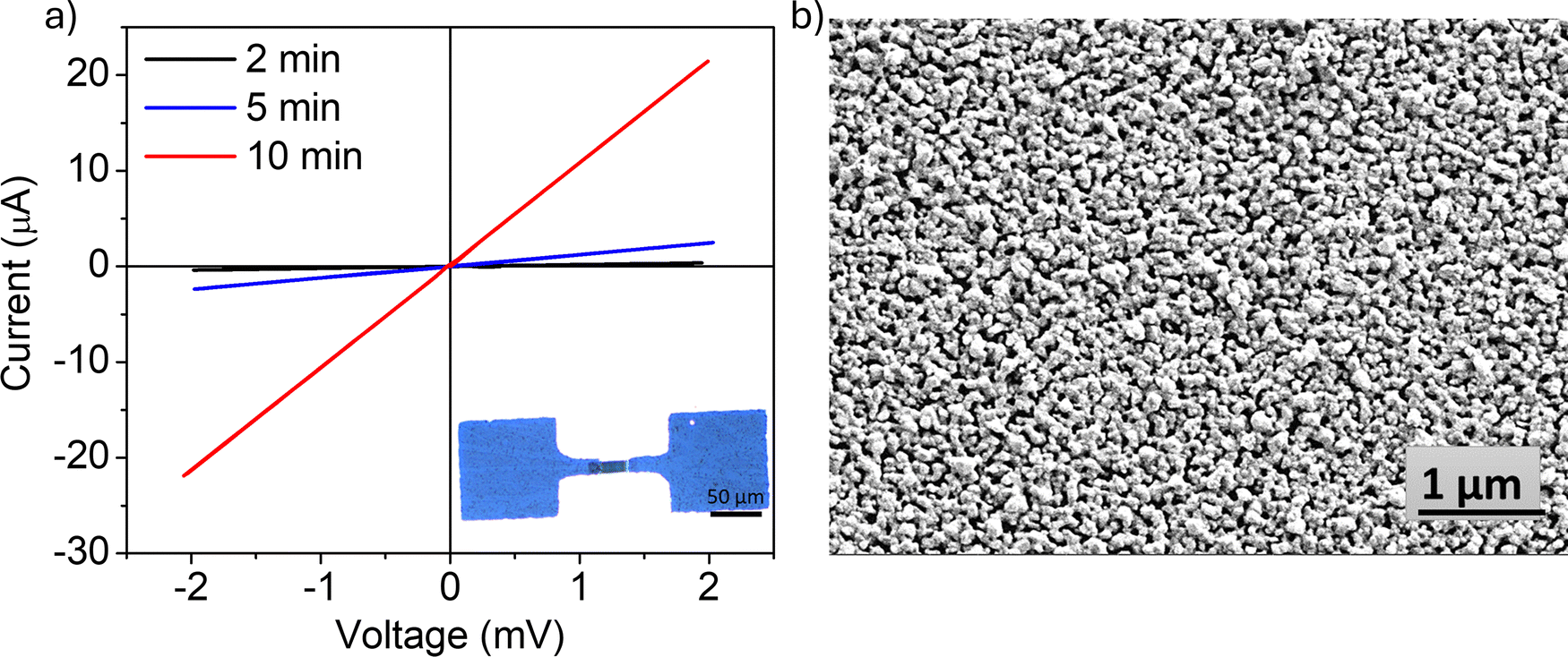 | ||
| Fig. 4 (a) I–V characteristics of the printed pattern obtained at various printing times. Inset shows the device photograph. (b) FESEM image of the printed structure. | ||
The optothermal trapping technique holds a significant advantage over the general particle trapping techniques.41–43 It uses low optical energy, thus not damaging the trapped particles, and can trap versatile particles. Having demonstrated the ability to easily print complicated structures, the printing technique is explored further for optothermal trapping of biological cells such as yeast cells. A plasmonic trap site of ∼8 μm diameter was printed on a glass substrate (Fig. 5a), and a 100 μL yeast solution was dropped on it after cleaning the substrate with DI water. After illuminating the printed pattern with white light, it was observed that the yeast cells were approaching the printed region and finally got trapped on the spot (Fig. 5a). During illumination, white light containing the plasmonic wavelength interacts with a printed plasmonic nanostructure which undergoes heating, generating a temperature gradient in the surrounding medium, with the irradiated region exhibiting the highest temperature. Such localized heating can induce various optothermal effects, including thermal convection, thermophoresis, and photophoresis. As demonstrated in our previous report, when the medium experiences localized heating due to photon absorption, the resulting convection-induced drag force drives dispersed particles laterally along the interface toward the hot zone. Simultaneously, a balance among the vertical components of thermal convection, thermophoretic force, and gravity enables particle trapping.33 To investigate the trapping stability, the trap site was continuously illuminated with white light for 10 minutes, and the trapping was monitored. After 10 min, the yeast cells were still present in the trap site, as shown in Fig. S12a–c (ESI†), thus signifying the stable trap. To avoid trapping ambiguity due to the physical attachment of the cell, the light was turned off to release the particles from the trap site. Interestingly, the particles moved away from the spot due to Brownian motion, thus validating the optothermal trapping (Fig. S12d–f, ESI†). Scaling up the optothermal trap sites is also important; thus, multiple plasmonic trap sites were printed in one shot, and importantly, the yeast cells were trapped in these sites (Fig. 5b). Moreover, parallel trapping of individual cells was also demonstrated using the plasmonic trap sites arranged in triangular geometry with an 8 μm diameter and 22 μm gap, as shown in Fig. 5c and d. Excitingly, white light could trap the cells optothermally, thus unveiling a non-laser-based approach, which has not been demonstrated so far.
 | ||
| Fig. 5 Optothermal trapping of yeast cells (a) on a single plasmonic printed structure, (b) parallel trapping using two printed spots, (c) illuminating three plasmonic trap sites individually with patterned white light and (d) trapping single yeast cells in each of the printed patterns. | ||
The efficacy of the printing technique is further demonstrated by printing Ag nanoparticles together with dye molecules such as crystal violet (CV), followed by its detection through surface-enhanced Raman spectroscopy. The study investigated how printing conditions affect Raman spectroscopy signals by using 1 μM of CV and maintaining a 1![[thin space (1/6-em)]](https://www.rsc.org/images/entities/char_2009.gif) :9 ratio with Ag nanoparticles. A set of six spots with different grayscale levels was patterned for 30 s (45 s) exposure, as shown in Fig. 6a and b (Fig. S13, ESI†). Variations in grayscale intensity led to different film fill factors, as is evident from the observed transparency in the optical image. The Raman signal intensity of the CV from the printed patterns was studied under the excitation of 532 nm, and the resulting variation in the Raman spectra is shown in Fig. 6c. Notably, the Raman signal varied for different patterns, and the variation in 1180 cm−1 band intensity is depicted in Fig. 6d. From the graph, it is evident that the signal intensity initially increases to reach a maximum, then decreases. This behavior suggests that the conditions leading to the second pattern in the first set (5% darker, 30 s printing time) and the third pattern in the second set (15% darker, 45 s printing time) are optimal for Raman studies, as these patterns give the highest intensity. The stability of the printed SERS platform is shown in Fig. S14 (ESI†).
:9 ratio with Ag nanoparticles. A set of six spots with different grayscale levels was patterned for 30 s (45 s) exposure, as shown in Fig. 6a and b (Fig. S13, ESI†). Variations in grayscale intensity led to different film fill factors, as is evident from the observed transparency in the optical image. The Raman signal intensity of the CV from the printed patterns was studied under the excitation of 532 nm, and the resulting variation in the Raman spectra is shown in Fig. 6c. Notably, the Raman signal varied for different patterns, and the variation in 1180 cm−1 band intensity is depicted in Fig. 6d. From the graph, it is evident that the signal intensity initially increases to reach a maximum, then decreases. This behavior suggests that the conditions leading to the second pattern in the first set (5% darker, 30 s printing time) and the third pattern in the second set (15% darker, 45 s printing time) are optimal for Raman studies, as these patterns give the highest intensity. The stability of the printed SERS platform is shown in Fig. S14 (ESI†).
 | ||
| Fig. 6 (a) Grayscale exposure design with different levels of brightness, (b) plasmonic patterns printed for 30 s along with crystal violet (CV), (c) Raman spectra of each spot and (d) intensity variation at 1180 cm−1 for different printed spots. | ||
Conclusions
This study presents a groundbreaking white light-based projection printing technique for fabricating plasmonic nanostructures. Utilizing a collimated light beam from the projector as a patterned light source, intricate patterns were successfully exposed to the colloidal solution of Ag nanoparticles. Due to plasmonic interactions and photon–phonon conversion, the nanoparticles get printed on the substrate, generating plasmonic nanostructures. Commendably, easy printing of arbitrary patterns such as hall bar electrodes, interdigitated electrodes, a photograph of Sir C. V. Raman, the MAHE logo, etc., was demonstrated. Notably, an impressive feature size of ∼400 nm is achieved, which can be further improved by using a high-contrast DMD-based projector. The patterning process was quick, taking only 5 s to print a structure with high resolution. Longer exposure led to nanoparticle coalescence, forming electrically conductive patterns without post-treatment. Prolonged illumination enhanced the conductivity further, suggesting the light-induced annealing process. This concept was exploited for the optothermal trapping of yeast cells using white light. Importantly, to the best of our knowledge, this is the first demonstration of non-laser-based optothermal trapping. As a scale-up approach, parallel trapping of the yeast cells was also showcased. The grayscale printing ability is exploited to investigate printing conditions for SERS study. Overall, the current technique surpasses traditional optical printing methods, offering the potential for the direct fabrication of devices and sensors, 2D optical components, and metasurfaces, thus paving the way toward advanced nanofabrication.Experimental section
Materials
AgNO3 (≥99.0%, Merck life science private limited), tri-sodium citrate dihydrate (≥99%, Merck life science private limited), crystal violet (88%, Loba Chemie Private limited), and yeast (Grain ‘N’ Grace Food Ingredients Manufacturing Private limited).Synthesis of the Ag nanoparticle solution
The Ag nanoparticle colloidal solution was prepared via the Lee and Meisel method. Briefly, 17 mg of AgNO3 was dissolved in 50 mL of deionized water and placed on a hotplate maintained at 90 °C. Then, a 40 mM solution of trisodium citrate was added dropwise to the solution and stirred magnetically until the color changed to golden yellow.Preparation of yeast cell solution
A yeast cell solution with a concentration of 0.1 mg mL−1 was prepared by dissolving dried yeast in water at room temperature.Characterization of Ag nanoparticles
The optical absorption spectra of the solution were recorded using a UV/Visible spectrophotometer (JASCO V650). The average particle size and zeta potential were measured with a Horiba Scientific nanoparticle size analyzer SZ-100. The Nikon Eclipse Ti2 inverted microscope was used for printing and imaging of the pattern. FESEM images were obtained using a Zeiss FESEM. I–V characteristics of the printed pattern were measured using a Keysight B2901B source measure unit. Raman signals were captured using a Horiba Scientific iHR-320 spectrometer coupled to the microscope.Projector printing setup
A commercial LCD projector (EPSON EB-X05) with a maximum brightness of 3300 lumens and XGA resolution is used for the printing setup. The diverging light beam from the projector was collimated using the microscope eyepiece and then passed through a simple Keplerian lens arrangement consisting of two biconvex lenses of focal lengths 30 mm and 200 mm to tune the image magnification. The light was then coupled to an inverted microscope configured with a beam splitter and a 100× oil immersion objective (NA = 1.45). Printing was performed on glass and quartz coverslips placed on the sample stage. A modified setup was also tried out to replace the eyepiece with a positive achromatic lens of 40 mm focal length.Data availability
Data will be made available on request.Conflicts of interest
There are no conflicts to declare.Acknowledgements
The authors gratefully acknowledge the Manipal Academy of Higher Education for the facility and funding support. Monisha K. acknowledges CSIR for a fellowship. Shreyas M. S. acknowledges the Dr T. M. A. Pai fellowship.Notes and references
- E. Sharma, R. Rathi, J. Misharwal, B. Sinhmar, S. Kumari, J. Dalal and A. Kumar, Nanomaterials, 2022, 12, 2754 Search PubMed.
- S. Jambhulkar, D. Ravichandran, Y. Zhu, V. Thippanna, A. Ramanathan, D. Patil, N. Fonseca, S. V. Thummalapalli, B. Sundaravadivelan, A. Sun, W. Xu, S. Yang, A. M. Kannan, Y. Golan, J. Lancaster, L. Chen, E. B. Joyee and K. Song, Small, 2024, 20, 2306394 Search PubMed.
- J. Li, E. H. Hill, L. Lin and Y. Zheng, ACS Nano, 2019, 13, 3783–3795 Search PubMed.
- N. Armon, E. Greenberg, E. Edri, O. Nagler-Avramovitz, Y. Elias and H. Shpaisman, Adv. Funct. Mater., 2021, 31, 2008547 Search PubMed.
- A. Kotnala and Y. Zheng, Part. Part. Syst. Charact., 2019, 36, 1900152 CrossRef PubMed.
- Z. Chai, A. Childress and A. A. Busnaina, ACS Nano, 2022, 16, 17641–17686 CrossRef CAS PubMed.
- M. J. Guffey and N. F. Scherer, Nano Lett., 2010, 10, 4302–4308 CrossRef CAS PubMed.
- C. Zhao, P. J. Shah and L. J. Bissell, Nanoscale, 2019, 11, 16187–16199 RSC.
- T. Takai, H. Nakao and F. Iwata, Opt. Express, 2014, 22, 28109 CrossRef PubMed.
- J. Li, Y. Liu, L. Lin, M. Wang, T. Jiang, J. Guo, H. Ding, P. S. Kollipara, Y. Inoue, D. Fan, B. A. Korgel and Y. Zheng, Nat. Commun., 2019, 10, 5672 CrossRef CAS PubMed.
- M. Mitmoen and O. Kedem, ACS Appl. Mater. Interfaces, 2022, 14, 32696–32705 CrossRef CAS PubMed.
- J. Li and Y. Zheng, Acc. Mater. Res., 2021, 2, 352–363 CrossRef CAS PubMed.
- C. M. Ragisha, N. M. Habeeb, V. L. Grace and S. N. Varanakkottu, Langmuir, 2024, 40, 12276–12287 CrossRef CAS PubMed.
- M. Kolikkaje, S. Karmegam, A. Bankapur and S. D. George, Anal. Chim. Acta, 2024, 1317, 342903 CrossRef PubMed.
- U. Zywietz, A. B. Evlyukhin, C. Reinhardt and B. N. Chichkov, Nat. Commun., 2014, 5, 3402 CrossRef PubMed.
- M. S. Alam and C. Zhao, ACS Omega, 2018, 3, 1213–1219 CrossRef CAS.
- J. A. Rodrigo, Sci. Rep., 2017, 7, 46506 CrossRef CAS.
- A. Mishra, K. Clayton, V. Velasco, S. J. Williams and S. T. Wereley, Microsyst. Nanoeng., 2016, 2, 16005 CrossRef CAS.
- E. H. Hill, C. Goldmann, C. Hamon and M. Herber, J. Phys. Chem. C, 2022, 126, 7622–7629 CrossRef CAS.
- P. S. Kollipara, R. Mahendra, J. Li and Y. Zheng, Aggregate, 2022, 3, e189 CrossRef CAS.
- L. P. Martinez, S. Poklepovich-Caride, J. Gargiulo, E. D. Martínez, F. D. Stefani, P. C. Angelomé and I. L. Violi, Nano Lett., 2023, 23, 2703–2709 CrossRef CAS PubMed.
- J. Gargiulo, I. L. Violi, S. Cerrota, L. Chvátal, E. Cortés, E. M. Perassi, F. Diaz, P. Zemánek and F. D. Stefani, ACS Nano, 2017, 11, 9678–9688 CrossRef CAS PubMed.
- J. Yan, K. Zhao, T. Wu, X. Liu, Y. Li and B. Li, ACS Appl. Mater. Interfaces, 2023, 15, 38682–38692 CrossRef CAS PubMed.
- A. S. Urban, A. A. Lutich, F. D. Stefani and J. Feldmann, Nano Lett., 2010, 10, 4794–4798 CrossRef CAS PubMed.
- S. Nedev, A. S. Urban, A. A. Lutich and J. Feldmann, Nano Lett., 2011, 11, 5066–5070 CrossRef CAS PubMed.
- J. Gargiulo, S. Cerrota, E. Cortés, I. L. Violi and F. D. Stefani, Nano Lett., 2016, 16, 1224–1229 CrossRef CAS PubMed.
- F. Schuknecht, C. M. Maier, P. Vosshage, V. A. Hintermayr, M. Döblinger and T. Lohmüller, Nano Lett., 2023, 23, 4762–4769 CrossRef CAS PubMed.
- J. Gargiulo, T. Brick, I. L. Violi, F. C. Herrera, T. Shibanuma, P. Albella, F. G. Requejo, E. Cortés, S. A. Maier and F. D. Stefani, Nano Lett., 2017, 17, 5747–5755 CrossRef CAS PubMed.
- A. J. Pascall, F. Qian, G. Wang, M. A. Worsley, Y. Li and J. D. Kuntz, Adv. Mater., 2014, 26, 2252–2256 CrossRef CAS PubMed.
- J. Mora, J. K. Dudoff, B. D. Moran, J. R. DeOtte, W. L. Du Frane, J. D. Kuntz and A. J. Pascall, Addit. Manuf., 2018, 22, 330–333 CAS.
- C. M. Jin, W. Lee, D. Kim, T. Kang and I. Choi, Small, 2018, 14, 1803055 CrossRef.
- L. Lin, X. Peng and Y. Zheng, Chem. Commun., 2017, 53, 7357–7360 RSC.
- M. Kolikkaje, S. Karmegam, A. Bankapur and S. D. George, Sens. Actuators, B, 2023, 377, 133047 CrossRef.
- C. E. Hoyle and C. N. Bowman, Angew. Chem., Int. Ed., 2010, 49, 1540–1573 CrossRef CAS PubMed.
- D. Walker, D. P. Singh and P. Fischer, Adv. Mater., 2016, 28, 9846–9850 CrossRef CAS PubMed.
- Y. Xie and C. Zhao, Nanoscale, 2017, 9, 6622–6631 RSC.
- B. B. Rajeeva, M. A. Alabandi, L. Lin, E. P. Perillo, A. K. Dunn and Y. Zheng, J. Mater. Chem. C, 2017, 5, 5693–5699 RSC.
- S. Ghosh, A. D. Ranjan, S. Das, R. Sen, B. Roy, S. Roy and A. Banerjee, Nano Lett., 2021, 21, 10–25 CrossRef CAS PubMed.
- N. Armon, E. Greenberg, M. Layani, Y. S. Rosen, S. Magdassi and H. Shpaisman, ACS Appl. Mater. Interfaces, 2017, 9, 44214–44221 CrossRef CAS PubMed.
- M. Herber, D. Lengle, S. R. Valandro, M. Wehrmeister and E. H. Hill, Nano Lett., 2023, 23, 6308–6314 CrossRef CAS PubMed.
- P. S. Kollipara, X. Li, J. Li, Z. Chen, H. Ding, Y. Kim, S. Huang, Z. Qin and Y. Zheng, Nat. Commun., 2023, 14, 5133 CrossRef CAS PubMed.
- J. Chen, Z. Chen, C. Meng, J. Zhou, Y. Peng, X. Dai, J. Li, Y. Zhong, X. Chen, W. Yuan, H.-P. Ho, B. Z. Gao, J. Qu, X. Zhang, H. Zhang and Y. Shao, Light: Sci. Appl., 2023, 12, 273 CrossRef CAS PubMed.
- S. Liu, L. Lin and H. B. Sun, ACS Nano, 2021, 15, 5925–5943 CrossRef CAS PubMed.
Footnote |
| † Electronic supplementary information (ESI) available. See DOI: https://doi.org/10.1039/d5mh00019j |
| This journal is © The Royal Society of Chemistry 2025 |