 Open Access Article
Optimized nano-scaled drain- and gate-engineered Schottky barrier MOSFET with improved ambipolarity and RF characteristics
Faisal
Bashir
 *,
Ali S.
Alzahrani
and
Furqan
Zahoor

Department of Computer Engineering, College of Computer Sciences and Information Technology, King Faisal University, Al-ahsa, Saudi Arabia. E-mail: famed@kfu.edu.sa; aalzahrani@kfu.edu.sa
First published on 1st November 2024
Abstract
In this work, a novel Schottky Barrier MOSFET (SB-MOSFET) structure is presented. The proposed device consists of a dual-material gate and electrostatically doped drain, and the device is denoted as Gate and Drain Engineered Schottky Barrier MOSFET (GDE-SBMOSFET). The use of a dual-material gate and electrostatically doped drain enhances the ON state performance and short channel performance, respectively, in comparison to state-of-the-art devices. By optimizing the gate and drain metal workfunction, the proposed device technology node can be scaled below 22 nm without exhibiting performance degradation. The optimized values of the metal workfunction of the drain and tunnel gate (TG) improve the parameters, such as the ON current and ON/OFF current ratio, which have been increased 26- and 10-fold in comparison to conventional SBMOSFETs. Additionally, a substantial enhancement of 28% and 4% in the SS of the proposed GDE-SBMOSFET has been achieved in comparison to that of the DSL and conventional SB-MOSFET, respectively. The ac investigation has shown that the cut-off frequency (fT) in the GDE-SBMOSFET (∼510 GHz) has increased 51 and 2 times as compared to that of the conventional SB-MOSFET (∼10 GHz). Further, the GDE-SBMOSFET has higher scalability and reduced ambipolarity, and doping-related issues caused by doped regions are absent in the proposed device.
1. Introduction
The performance enhancement of MOSFETs depends heavily on their dimensions. Reducing the size of MOSFETs has led to significant advancements in terms of speed, packaging density, power dissipation, and cost. However, scaling these devices below 32 nm becomes challenging due to issues such as gate oxide tunneling, drain tunneling, doping-related problems, parasitic effects, and short channel effects (SCE).1–3 Various methods have been proposed by researchers to address these challenges,4–11 with ultra-thin junctions and heavily doped source/drain (S/D) regions being considered effective solutions. SB-MOSFETs (Schottky Barrier MOSFETs) combine these properties,12 making them an essential approach to tackling SCEs and reducing large the RSD (source drain resistance). Moreover, SB-MOSFET offers additional benefits, including better control over off-state current, lower parasitic capacitance, increased channel mobility due to undoped channel doping, simpler and more cost-effective S/D realization process, scalability, rejection of parasitic bipolar effects, and a comparatively straightforward fabrication procedure.13,14In spite of these advantages, Schottky barriers have drawbacks. In the off-state, leakage current primarily occurs due to thermal emission, which requires a high Schottky barrier to suppress it. Conversely, a zero-height barrier is preferable for achieving significant on-current during the on-state. Therefore, there is always a trade-off between these two requirements. A low Schottky barrier improves the on-state tunneling current but reduces the ION/IOFF ratio due to increased off-state leakage current.15,16 Researchers have proposed different approaches for enhancing the ION/IOFF ratio through the reduction of the Schottky barrier height. One successful method discussed in ref. 10, 17 and 18 involves employing a dopant segregation layer to modulate the barrier. However, this technique is laborious and increases the complexity and thermal requirements during device fabrication. Another proposed solution is the utilization of nano-scaled SB-MOSFETs, in which shorter spacer lengths are utilized to amplify the fringing fields on the barrier. This, in turn, improves the device's driving capability, as mentioned in ref. 19. Additionally, the performance of SB-MOSFETs can be improved by implementing an ultrathin silicon-on-insulator (SOI) substrate, which enhances the carrier injection capability of the SB, as demonstrated in ref. 20–22. An alternative approach presented in my previous work 9,10 involves the use of an extended source, but its fabrication becomes considerably challenging at sub-10 nm scales. In addition to this, there is an ambipolarity issue in SB-FETs, which deteriorates the performance of the SB-FETs. Several studies have addressed this issue, and some solutions, such as 2D material-based devices, have been proposed in the literature.23–26 However, the mass fabrication of 2D materials is still in its infancy.
This paper investigates the performance of a new type of SB-MOSFETs (Schottky Barrier MOSFETs) compared to that of conventional ones through a detailed comparative analysis. The proposed device utilizes a metal silicide (ErSi1.4) in the source/drain region and an undoped silicon material in the channel. The use of silicides is advantageous, as they can be easily realized at low temperatures,27 and their low resistance makes them appropriate for nodes of less than <10 nm. The proposed device incorporates gate and drain engineering, which enhances its resistance to SCEs (short channel effects). Furthermore, the top gate of the device uses two metal workfunctions and has a low metal workfunction gate near the source channel junction. Various performance parameters, including ION, ION/IOFF, transconductance (gm), and other analog/RF application parameters, have been calculated. The results indicate that the proposed device outperforms both conventional devices and the current state-of-the-art devices.
This paper is divided into four sections. Section II discusses device structures and simulation parameters of the conventional and the proposed devices. Section III discusses results. Section IV concludes the paper.
2. Structural description and simulation parameters
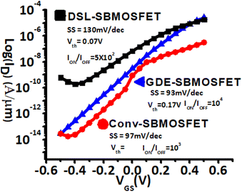
Atlas Silvaco TCAD28 was used to carry out simulations of the conventional, DSL-SBMOSFET and proposed GDE-SBMOSFET device structure. For accurate comparative analysis, various models were used in the TCAD simulations, namely, srh, fermi, consrh, drift diffusion, conmob, fldmob and ust. The transport of carriers in the channel is mainly governed by the drift diffusion model. The tunneling across the metal semiconductor junction is captured by the Schottky tunneling model (ust), whereas conmob and fldmob mobility models were used to capture the field- and concentration-dependent mobility. In addition to this, the band-to-band tunneling model (BTBT) was used in the proposed device to check the tunneling at the drain channel interface.The schematics of the conventional, dopant segregation layer (DSL) and proposed Gate and Drain Engineered (GDE) Schottky Barrier MOSFET devices studied in this work are shown in Fig. 1. In the calibration of the model, the device structure, including its dimensions and other parameters, remained consistent with those utilized in ref. 19 for generating simulation data. Fig. 1d demonstrates the remarkable agreement between the simulated results and the experimental data reported in ref. 19. In the proposed GDE-SBMOSFET structure, the drain has been realized electrostatically using the optimized metal workfunction and the gate consists of two types of material, denoted as the Tunnel Gate (TG) and Main Gate (MG). The TG has a low metal workfunction and is responsible for modulating the barrier width at the Source Channel interface in the proposed device. The summarized device design parameters for all the devices can be found in Table 1. Upon conducting a comprehensive analysis of the device, it is evident that the GDE-SB-MOSFET exhibits a noteworthy band bending effect.
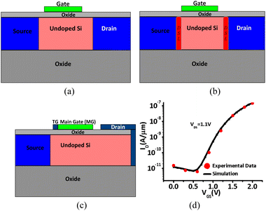 | ||
| Fig. 1 Schematics of (a) conventional SBMOSFET, (b) DSL SBMOSFET and (c) proposed GDE-SBMOSFET. (d) Model Calibration using experimental data. 19 | ||
| Parameter | Conv. SBMOSFET | DSL-SBMOSFET | Proposed GDE-SBMOSFET |
|---|---|---|---|
| Gate length | 20 nm | 20 nm | 20 nm |
| Oxide thickness | 1 nm | 1 nm | 1 nm |
| Undoped Si thickness | 8 nm | 8 nm | 8 nm |
| Length of device | 100 nm | 100 nm | 100 nm |
| Gate work function | 4.72 eV | 4.72 eV | 4.9 eV and 4.65 eV |
| DSL doping conc | NA | 6 × 1019 cm−3 | NA |
| Drain metal workfunction | 4.5 eV | 4.5 eV | 3.9 eV |
| Source metal workfunction | 4.5 eV | 4.5 eV | 4.5 eV |
| Width of tunnel gate | NA | NA | 2 nm |
| Work of tunnel gate | NA | NA | 3.7 eV |
| L Gap,Drain | NA | NA | 4 nm |
3. Process flow for the GDE-SBMOSFET
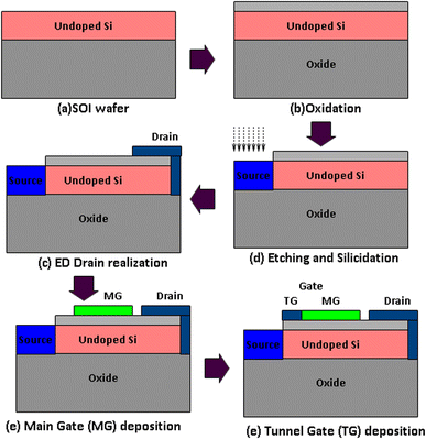
This band bending plays a crucial role in enhancing various parameters such ION, ION/IOFF ratio, SS, gm, fT and other related parameters.The possible steps for the fabrication for the proposed GDESB-FET are shown in Fig. 2. The device would be fabricated on a lightly doped (1016 cm−3) p-type silicon substrate, followed by metal silicidation. In order to achieve precise control over depth and ensure high smoothness with less than 1 nm roughness on the vertical walls and edges, lithography was performed, followed by CF4 plasma oxide etching at a temperature of −20 °C.29 The deposition of the tunnel gate and main gate electrodes would be carried out using a metallization process. To lower the deposition temperature, a method called plasma-enhanced chemical vapor deposition (PECVD) would be employed. Alternatively, low-pressure chemical vapor deposition (LPCVD) could also be utilized to attain higher purity, uniformity, and reduced chemical contamination.30,31
4. Results and discussion
4.1. DC characteristics
The band diagrams (BD) of DSL-SBMOSFET and GDE-SB-MOSFET in the ON- and OFF-states are shown in Fig. 3.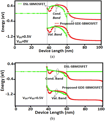 | ||
| Fig. 3 Energy band diagram of the conventional and proposed device in the (a) OFF state (VDS = 0.5 V, VGS = 0 V) and (b) ON state (VDS = VGS = 0.5 V). | ||
It is clear from the Fig. 2 that barrier width at the source and channel interface has been modulated by using the DSL and tunnel gate (TG) in the DSL-SBMOSFET and GDE-SBMOSFET respectively, and the modulation of the barrier width is more effective in the GDE-SBMOSFET. Additionally, the barrier height in the channel is higher in the case of GDE-SBMOSFET; therefore, the proposed device is less susceptible to short channel effects compared to the DSL and Conventional SBMOSFET. The enhancement in performance characteristics of the GDE-SBMOSFET as compared to the conventional devices can be due to the efficient use of the electrostatically doped drain and gate engineering concepts.
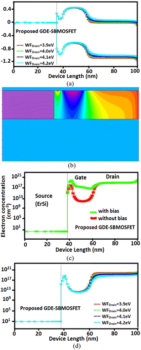
Fig. 4 shows the effect of the drain metal workfunction on the energy bands and electron concentration in the GDE-SBMOSFET. It was observed that lowering the metal workfunction increases the electron concentration and lowers the energy bands. The device profile of the GDE-SBMOSFET for 3.9 eV drain metal workfunction is shown in Fig. 4(b), where the formation of charge plasma is visible.
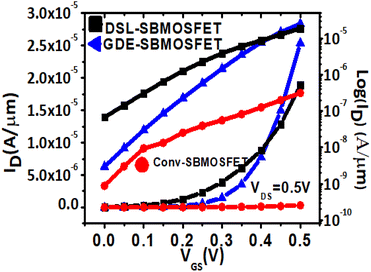
The device characteristics of all the device structures as calculated at VDS = VGS = 0.5 V are shown in Fig. 5. The ION of the GDE-SBMOSFET is 26 μA μm−1, while those of the DSL-SBMOSFET and conventional SBMOSFET are 20 μA μm−1 and 1 μA μm−1, respectively. The ION/IOFF ratio of the GDE-SBMOSFET (1 × 10⁴) is enhanced by about ∼100 and 10 times compared to those of the DSL-SBMOSFET (2 × 10²) and conventional SBMOSFET (1 × 10³) counterparts, respectively. This outstanding performance in the GDE-SBMOSFET can be attributed to the band bending in the channel of the GDE-SBMOSFET, as is evident from the EBD in Fig. 3. There is a 28% and 4% improvement in the subthreshold swing in the GDE-SBMOSFET (93 mV dec−1) compared to that of the DSL-SBMOSFET (130 mV dec−1) and conventional SBMOSFET (97 mV dec−1).
Fig. 6 shows the ambipolarity behavior of all three devices under consideration. It was observed that GDE-SBMOSFET exhibits almost no ambipolar current; therefore, circuits designed using GDE-SBMOSFET can have low short-circuit power dissipation. The lower ambipolar conduction in the GDE-SBMOSFET can be attributed to the electrostatically designed drain in the GDE-SBMOSFET. The use of an optimized workfunction at the drain electrode controls the ambipolar current.
Fig. 7 shows the effect of the gate drain gap (LGap,Drain) and drain metal workfunction on the performance of the proposed device.
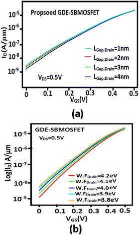 | ||
| Fig. 7 Impact of (a) gate drain gap (LGap,Drain) and (b) drain metal workfunction (W.FDrain) on the performance of the proposed device. | ||
It was observed that as the gap and workfunction increase, the leakage decreases. The increase in the gap and workfunction widens the energy band at the drain channel interface and thus improves the leakage.
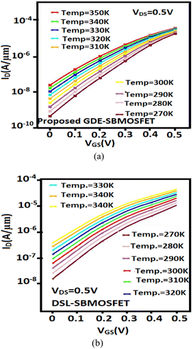
Fig. 8 shows the influence of the temperature on the transfer characteristics of the GDE-SBMOSFET and DSL-SBMOSFET. It was observed that the GDE-SBMOSFET shows a weak dependence in the ON state as compared to the conventional device. This weak dependence can be attributed to the tunnel gate and electrostatically doped drain. The charge concentration created beneath the tunnel gate varies with the depth, whereas the DSL shows constant variation with depth, which results in a variable Schottky barrier width in proposed device.
4.2. AC analysis
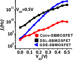
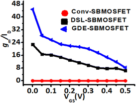
Fig. 9 shows the plot of the cutoff frequency against the gate voltage at a constant drain voltage. It was found that a higher value of fT was observed in GDE-SBMOSFET.The higher value of fT may be due to the higher transconductance and lower capacitance in the proposed device in comparison to the conventional devices. Fig. 10 shows the transconductance generation factor (gm/ID) of all three devices. It was observed that the gm/ID is higher in the GDE-SBMOSFET over the entire range of gate voltages.
It was observed that the gm/ID of the proposed device was much higher for entire VGS range. The higher value of gm/ID for the proposed device may be due to the higher driving and transconductance in the proposed device.
4.3. Impact of gate length scaling
The influence of different gate length dimensions on the performance-measuring parameters is shown in Fig. 11. The effect of the gate length on threshold voltage (Vth) and subthreshold swing (SS) of the GDE-SB-MOSFET and DSL-SB-MOSFET is shown in Fig. 10a. It was found that the GDE-SB-MOSFET technology node can be scaled well below 12 nm without any performance loss as compared to DSL-SB-MOSFET. The leakage current is significantly lower in GDE-SB-MOSFET as compared to DSL-SB-MOSFET for all gate lengths, as shown in Fig. 11b. Fig. 11c presents the variation in the cut-off frequency (fT) and ON current with respect to gate length. Both the fT and ON current are higher in the GDE-SB-MOSFET as compared to DSL-SB-MOSFET.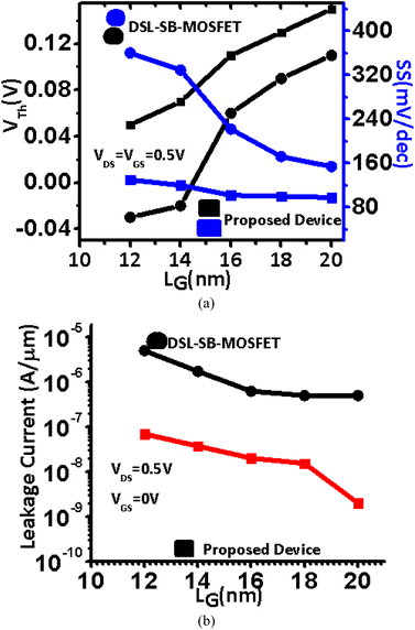 | ||
| Fig. 11 Impact of gate length scaling on (a) threshold voltage, sub-threshold swing and (b) leakage current of the GDE-SBMOSFET and DSL-SBMOSFET. | ||
It was observed that optimization of the drain metal workfunction and tunnel gate metal workfunction played a major role in obtaining significantly improved performance in the measured parameters of the GDE-SB-MOSFET.
The performance of the proposed device was compared with those reported in the previously published works on SB-MOSFETs and is summarized in Table 2. From the table, it can be seen that the proposed device presents comparatively very good performance considering the employed gate length and supply voltages. Additionally, the proposed device suppresses the ambipolar current, which is an important concern with SB-MOSFETs. The ambipolarity issue was not addressed by most of the works presented in the table.
4.4. Circuit level implementation
The circuit-level analysis of the devices involved designing inverters and examining the transient response of inverters based on the GDE-SBMOSFET and conventional SB-MOSFET, as illustrated in Fig. 12. The findings indicated that the inverter circuit utilizing the GDE-SBMOSFET exhibits shorter OFF and ON delays compared to the one employing the conventional SBMOSFET. The calculated percentage decrease in the ON delay is 98%, indicating that the SB-MOSFET-based inverter has a lower delay. Similarly, the OFF delay of the inverter using GDE-SBMOSFET is reduced, with a percentage decrease of 50%. This reduction in both the ON and OFF delays results in the circuit designed with GDESB-MOSFET being faster, effectively reducing the average delay of the circuit.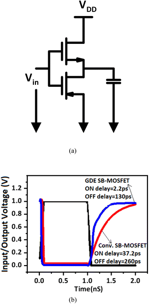 | ||
| Fig. 12 (a) SB-MOSFET-based inverter circuit. (b) Transient analysis of the proposed and conventional SB-MOSFET. | ||
5. Conclusion
A novel Schottky Barrier MOSFET structure with an engineered drain and gate has been presented in this study. The proposed device outperforms the conventional devices in terms of various performance measurement parameters, such as the ON current and ON/OFF current ratio, which were increased 26- and 10-fold in comparison to the conventional SBMOSFETs. Additionally, considerable improvements in the SS of 28% and 4% have been achieved by the proposed GDE-SBMOSFET in to the comparison to DSL and conventional SB-MOSFET, respectively. The cut-off frequency (fT) in the GDE-SBMOSFET (∼510 GHz) has increased 51 and 2 times as compared to that of the conventional SB-MOSFETs. The TG modulates the barrier width of the source and channel interface and controls the ON-state performance measurement parameters, whereas the optimized value of the drain metal workfunction controls the OFF-state performance and SCEs. It has been observed that proposed device is less prone to SCEs and possesses no ambipolar behavior.Data availability
Information regarding the data may be available upon request, subject to confidentiality agreements.Conflicts of interest
There are no conflicts to declare.Acknowledgements
This work was funded and supported by King Faisal University, Eastern Region, Al-Ahsa, Saudi Arabia under grant number KFU242271. We would like to express our sincere gratitude to the funding organization that supported this research project. Their financial support was instrumental in the successful completion of this study.References
- R. H. Dennard, F. H. Gaensslen, H.-N. Yu, V. L. Rideout, E. Bassous and A. R. Leblanc, Design of ion-implanted MOSFETs with very small physical dimensions, IEEE J. Solid-State Circuits, 1974, SSC-9(5), 256–268 Search PubMed
.
- S. A. Loan, S. Qureshi and S. S. K. Iyer, A novel partial ground plane based MOSFET on selective buried oxide: 2D simulation study, IEEE Trans. Electron Devices, 2010, 57, 671–680 Search PubMed
.
-
M. Ostling, J. Luo, V. Gudmundsson, P. E. Hellström and B. G. Malm, Nanoscaling of MOSFETs and the implementation of Schottky barrier S/D contacts, Proc 27th Int Conf Microelectron, 2010, pp. 9–13 Search PubMed
.
- G. Larrieu, D. A. Yarekha, E. Dubois, N. Breil and O. Faynot, Arsenic-segregated rare-earth silicide junctions: Reduction of Schottky barrier and integration in metallic n-MOSFETs on SOI, IEEE Electron Device Lett., 2009, 30(12), 1266–1268 CAS
.
- R. Vega and T. J. K. Liu, Dopant-segregated Schottky junction tuning with fluorine pre-silicidation ion implant, IEEE Trans. Electron Devices, 2010, 57(5), 1084–1092 Search PubMed
.
-
J. P. Snyder, The Physics and Technology of Platinum Silicide Source and Drain Field Effect Transistors [dissertation], Stanford, CA, Stanford Univ., 1996 Search PubMed
.
- G. Larrieu and E. Dubois, Schottky-barrier source/drain MOSFETs on ultrathin SOI body with a tungsten metallic midgap gate, IEEE Electron Device Lett., 2004, 25(12), 801–803 CrossRef CAS
.
-
S. A. Loan, F. Bashir, M. Rafat, A. R. M. Alamoud and S. A. Abbasi, A high performance double gate dopingless metal oxide semiconductor field effect transistor, Proc IEEE 20th Int Conf Ion Implant Technol (IIT), 2014 Search PubMed
.
- F. Bashir, S. A. Loan, M. Rafat, A. R. M. Alamoud and S. A. Abbasi, A high-performance source engineered charge plasma-based Schottky MOSFET on SOI, IEEE Trans. Electron Devices, 2015, 62(10), 3357–3364 CAS
.
- F. Bashir, A. G. Alharbi and S. A. Loan, Electrostatically Doped DSL Schottky Barrier MOSFET on SOI for Low Power Applications, IEEE J. Electron Devices Soc., 2017, 6, 19–25 Search PubMed
.
- F. Bashir, A. M. Murshid, F. A. Khanday and M. T. Banday, Impact of Pocket Doping On the Performance of Planar SOI Junctionless Transistor, Silicon, 2021, 13, 1771–1776 CrossRef CAS
.
- M. P. Lepselter and S. M. Sze, SB-IGFET: an insulated-gate field effect transistor using Schottky barrier contacts for source and drain, Proc. IEEE, 1968, 56(8), 1400–1402 Search PubMed
.
- R. Vega and T. J. K. Liu, Dopant-segregated Schottky junction tuning with fluorine pre-silicidation ion implant, IEEE Trans. Electron Devices, 2010, 57(5), 1084–1092 Search PubMed
.
-
J. P. Snyder, The Physics and Technology of Platinum Silicide Source and Drain Field Effect Transistors [dissertation], Stanford, CA, Stanford Univ., 1996 Search PubMed
.
- G. Larrieu and E. Dubois, Schottky-barrier source/drain MOSFETs on ultrathin SOI body with a tungsten metallic midgap gate, IEEE Electron Device Lett., 2004, 25(12), 801–803 CrossRef CAS
.
- M. Fritze, C. L. Chen, S. Calawa, D. Yost, B. Wheeler and P. Wyatt,
et al., High-speed Schottky-barrier pMOSFET with f/sub T/= 280 GHz, IEEE Electron Device Lett., 2004, 25, 220–222 CrossRef
.
- G. C. Patil and S. Qureshi, A novel δ-doped partially insulated dopant segregated Schottky barrier SOI MOSFET for analog/RF applications, Semicond. Sci. Technol., 2011, 26(8), 085002 CrossRef
.
- G. Larrieu and E. Dubois, CMOS inverter based on Schottky source–drain MOS technology with low-temperature dopant segregation, IEEE Electron Device Lett., 2011, 32(6), 728–730 CAS
.
- R. Jhaveri, V. Nagavarapu and J. C. S. Woo, Asymmetric Schottky Tunneling Source SOI MOSFET Design for Mixed-Mode Applications, IEEE Trans. Electron Devices, 2009, 56(1) CAS
.
- Y. K. Chin, K. L. Pey, N. Singh, G. Q. Lo, K. H. Tan and C. Y. Ong,
et al., Dopant-segregated Schottky silicon-nanowire MOSFETs with gate-all-around channels, IEEE Electron Device Lett., 2009, 30, 843–845 CAS
.
- M. Zhang, J. Knoch, J. Appenzeller and S. Mantl, Improved carrier injection in ultrathin-body SOI Schottky-barrier MOSFETs, IEEE Electron Device Lett., 2007, 28(3), 223–225 CAS
.
- S. Zhu, H. Y. Yu, J. D. Chen, S. J. Whang, J. H. Chen and C. Shen,
et al., Low temperature MOSFET technology with Schottky barrier source/drain, high-K gate dielectric and metal gate electrode, Solid-State Electron., 2004, 48(10–11), 1987–1992 CrossRef CAS
.
- Z. Q. Fan, Z. H. Zhang and S. Y. Yang, High-performance 5.1 nm in-plane Janus WSeTe Schottky barrier field effect transistors, Nanoscale, 2020, 12, 21750–21756 RSC
.
- Q. Liu, J. J. Li, D. Wu, X. Q. Deng, Z. H. Zhang, Z. Q. Fan and K. Q. Chen, Gate-controlled reversible rectifying behavior investigated in a two-dimensional MoS2 diode, Phys. Rev. B, 2021, 104, 045412 CrossRef CAS
.
- X. D. Huang,
et al., Transport Properties of 5-nm Tunnel Field-Effect Transistor for High-Performance Switches Decorated With Blue Phosphorene and Transition Metals, IEEE Trans. Electron Devices, 2023, 70(10), 5462–5468 CAS
.
- F. Zahoor, M. Hanif, U. I. Bature, S. Bodapati, A. Chattopadhyay, F. A. Hussin, H. Abbas, F. Merchant and F. Bashir, Carbon nanotube field effect transistors: an overview of device structure, modeling, fabrication and applications, Phys. Scr., 2023, 98, 082003 CrossRef CAS
.
- S. Zhu, H. Y. Yu, J. D. Chen, S. J. Whang, J. H. Chen and C. Shen,
et al., Low temperature MOSFET technology with Schottky barrier source/drain, high-K gate dielectric and metal gate electrode, Solid-State Electron., 2004, 48(10–11), 1987–1992 CrossRef CAS
.
-
ATLAS Device Simulation Software, Silvaco Int., Santa Clara, CA, USA, 2018 Search PubMed
.
- M. Guilmain, A. Jaouad, S. Ecoffey and D. Drouin, SiO2 shallow nanostructures ICP etching using ZEP electroresist, Microelectron. Eng., 2011, 88(8), 2505–2508 CrossRef CAS
.
- X. Y. Zhang, C. H. Hsu, S. Y. Lien, S. Y. Chen, W. Huang and C. H. Yang,
et al., Surface passivation of silicon using HfO2 thin films deposited by remote plasma atomic layer deposition system, Nanoscale Res. Lett., 2017, 12(1), 1–7 CrossRef PubMed
.
-
N. Alfaraj and N. A. Rasheedi, Fabrication Simulation of a Flexible Metal–Oxide–Semiconductor Field-Effect Transistor, 2018, DOI:10.13140/RG.2.2.32243.12324/1
.
- P. Kumar and B. Bhowmick, Source-Drain Junction Engineering Schottky Barrier MOSFETs and their Mixed Mode Application, Silicon, 2020, 12(4), 821–830 CrossRef CAS
.
| This journal is © The Royal Society of Chemistry 2025 |

