
 Open Access Article
 This Open Access Article is licensed under a Creative Commons Attribution-Non Commercial 3.0 Unported Licence
Toward nanofabrication of SERS substrates with two-photon polymerization†
Tatevik
Chalyan
 *a,
Mehdi
Feizpour
a,
Qing
Liu
a,
Koen
Vanmol
a,
Núria
Solerdelcoll
a,
Gen
Takebe
ab,
Hugo
Thienpont
a and
Heidi
Ottevaere
a
*a,
Mehdi
Feizpour
a,
Qing
Liu
a,
Koen
Vanmol
a,
Núria
Solerdelcoll
a,
Gen
Takebe
ab,
Hugo
Thienpont
a and
Heidi
Ottevaere
a
aBrussels Photonics (B-PHOT), Department of Applied Physics and Photonics, Vrije Universiteit Brussel and Flanders Make, Pleinlaan 2, B-1050 Brussels, Belgium. E-mail: tatevik.chalyan@vub.be
bCentral Research Laboratory, Hamamatsu Photonics K.K., 5000, Hirakuchi, Hamana-ku, Hamamatsu, Shizuoka, Japan
First published on 17th December 2024
Abstract
Surface-enhanced Raman spectroscopy (SERS) has shown its ability to characterize biological substances down to a single-molecule level without a specific biorecognition mechanism. Various nanofabrication technologies enable SERS substrate prototyping and mass manufacturing. This study reports a complete cycle of design, fabrication, prototyping, and metrology of SERS substrates based on two-photon polymerization (2PP). Highly controllable direct laser writing allows the fabrication of individual nanopillars with up to an aspect ratio of 4. The developed SERS substrates show up to 106 Raman signal enhancement, comparable to commercial substrates. Moreover, the rapid prototyping of the 2PP-printed SERS substrates takes from a minute to less than 2 hours, depending upon the nano-printing approach and aspect ratio requirements. The process is well-controlled and reproducible for achieving a uniform distribution of nanostructure arrays, allowing the SERS substrates to be used for a broad range of applications and the characterization of different molecules.
1. Introduction
Among the various optical biosensing techniques, those based on Raman scattering have become more popular in the past decade and applied in different fields, both in academic research and clinical studies.1 One of the key advantages of Raman spectroscopy is its non-destructive nature, which makes it suitable for analyzing sensitive samples.2 On the other hand, Raman scattering is a very weak effect, which leads to a low sensitivity, making it difficult to measure low concentrations of a substance. Surface-enhanced Raman spectroscopy (SERS) enhances the Raman signal and further improves this powerful tool via localized surface plasmon resonance triggered when the laser frequency aligns with the oscillation frequency of the electrons on the metallic surfaces in the neighborhood of analyte's molecules thus boosting the intensity of the Raman signal.3 It is possible to improve the SERS signal even further by manipulating the energy bands of the molecules by using techniques such as ferroelectric polarization.4 SERS uses substrates such as nanoparticles (NPs) and planar nanostructures including meta-structures.5 The latter is attracting great interest because of their convenient integration into lab-on-a-chip (LOC) devices. Given this increasing interest, the primary emphasis of planar SERS substrate development is currently on their structural uniformity,6 customization,7 and implementation.8,9 In the earlier work published by our group, the effect of structural homogeneity and hotspot density on the Raman signal has been studied using different commercial SERS substrates.10 A higher structural order leads to a lower spatial Raman signal instability and, subsequently a better reproducibility and imaging resolution. Moreover, smaller gaps between the nanostructures lead to stronger hotspots and smaller features lead to a higher density of hotspots, consequently improving the Raman signal's intensity and reproducibility. Commercial SERS substrates, such as from Hamamatsu11 and Silmeco,12 use nanoimprinting and reactive ion etching techniques, respectively. While these techniques prioritize manufacturing speed, they may compromise precise control over the resulting structures. Consequently, quality parameters like the nanostructures' homogeneity, pattern, and feature shapes are inaccessible to these fabrication techniques, while they hold great potential for SERS performance improvement.13,14 Furthermore, lithographic techniques are widely used to create precise and consistent nanostructures.15 However, elaborate preparation processes and expensive equipment hinder their use. Therefore, the field of planar SERS substrates, known for its high potential for reproducible sensing applications and ease of implementation, lacks a 3D prototyping technology that can quickly study a variety of different nanostructure architectures.Two-photon polymerization (2PP), an additive 3D printing technology, can be a cost-efficient alternative for controlled prototyping of SERS nanostructures.16 It is a 3D printing method that employs ultrafast pulsed laser beams to initiate polymerization in a photosensitive material or photoresin. This process is activated when two photons are absorbed simultaneously, allowing for high spatial resolution and precision. The 2PP technique enables rapid prototyping of customized nanostructures, thereby optimizing the enhancement effect for specific applications.17 Only a few published works have combined SERS with the 2 PP technique. Our group previously presented research results on fabricating nanopillar arrays on flat substrates using 2PP for SERS substrate fabrication to detect mycotoxins18 and vitamin D.19 Kim et al. also reported the fabrication of fiber-optic SERS probes using 2PP for bacterial detection.20 These studies demonstrated promising detection capabilities by employing 2PP-fabricated nanostructures as SERS substrates. However, a comprehensive investigation of the influence of the 2PP resolution on the SERS performance is notably absent in existing research.
In this study, we aim to use the prototyping capabilities of 2PP to achieve a uniform distribution of tightly packed nanopillars, showcasing the potential of this technique for SERS. Optimization of nano-printing parameters such as pillar height and pitch was performed considering the structural dimension limitations inherent to the 2PP process, which are significantly influenced by laser power and light–matter interaction. Recalling the recent work from our group21 focusing on Finite-Difference Time-Domain (FDTD) simulations to find the most favorable range of the nano-printing parameters, several combinations of the pillar height and pitch were fabricated in this research. Single-voxel and multivoxel 2PP approaches were investigated with the Galvano-mirror and piezo-stage scanning mode,22 respectively. Depending on the fabrication approach, 50 × 50 μm2 SERS substrates were fabricated within several minutes to less than 2 hours. Through atomic force microscopy (AFM) and scanning electron microscopy (SEM) images, we studied the morphology of the printed SERS substrates and compared them to commercial substrates. These substrates were benchmarked using our previously developed and reported characterization protocol against Silmeco and Hamamatsu commercial SERS substrates, which exhibit, respectively, the highest and most uniform Raman signals.10 The 2PP-printed substrates had comparable or in some cases better SERS performance to the Hamamatsu substrates, both in terms of performance and uniformity. This fabrication method of highly controlled and reproducible SERS substrates paves the way towards fast prototyping of a label-free and ligand-free optical biosensor for the detection of a variety of analytes.
2. Experimental
To achieve state-of-the-art SERS substrates with 2PP, a full cycle from simulations to prototyping and metrology is realized. This section will provide details about the fabrication process, metrology tools, measurement protocols, and modeling and data processing approaches.2.1 Materials
The 25 × 25 mm2 fused silica substrates obtained from nanoscribe were silanized using 3-(trimethoxysilyl)propyl methacrylate (Merck KGaA, Darmstadt, Germany) for 30 min. Immersing the glass substrate into a solution composed of 50 μL of 3-(trimethoxysilyl)propyl methacrylate mixed in 25 mL acetone improved the adhesiveness of the photoresin on the fused silica glass. Proprietary IP-Dip2 photoresin was obtained from Nanoscribe. It was designed for Dip-in Laser Lithography (DiLL), which serves as an immersion and photosensitive material. The microscope objective was dipped into the photoresin during the fabrication. IP-Dip2 is used for the highest-resolution 3D nanofabrication and does not require the fabrication of pre- or post-baking steps.23 After the 2PP process, the non-polymerized IP-Dip2 was washed away using the developer. For ten minutes, the fused silica substrate was immersed in propylene glycol methyl ether acetate (PGMEA) Sigma-Aldrich. Subsequently, it was cleaned with isopropanol and dried in dry air. A gold target with 19.3 g cm−3 density purchased from JEOL, was used to coat the substrates. Gold was selected over other metals such as silver because of its superior biocompatibility.24Next, 1,2-bis-(4-pyridyl) ethylene (BPE) purchased from Sigma-Aldrich was used for SERS measurements. The stock solution, that is, 1 mM of BPE in ethanol, was prepared by mixing 15 mL of 99,7% purity ethanol with 2.7 mg BPE, considering its molecular weight at 182.22 g mol−1. The lower concentrations used during the experiments given in this study were derived by diluting the stock solution in ethanol.
2.2 Instrumentation
The structures are fabricated using two-photon polymerization with the Nanoscribe Photonic Professional GT+ system. The device uses an inverted microscope with a 63× magnification objective to focus a femtosecond pulsed laser beam of 780 nm in the liquid photoresin to initiate the two-photon polymerization reaction of the material, leading to locally solidified zones. The laser power is controlled using an acousto-optic modulator (AOM). By moving the laser beam (or the sample with photoresin), the desired structure is inscribed in the material, polymerizing adequate zones, typically layer-by-layer as shown in Fig. 1 ESI.† The smallest polymerized volume of photoresin from a single light–matter interaction is called a voxel and has an ellipsoidal shape. Its dimensions depend on the laser spot and chemical characteristics.22 The height of the nanoprinted structures highly depends on the height of the voxel. Nanoscribe's proprietary software, DeScribe, is utilized to control the movements of the stages and other printing parameters, such as the laser power and printing speed. In this study, two different modes of the sample holder stage and laser beam movements were used, to obtain the 3D structures. First, single-voxel-based SERS substrates were fabricated. The laser spot positioning along the sample plane (i.e., the X and Y directions) is controlled by Galvano mirrors, thus polymerizing the photoresin material and creating an array of nanopillars. Accurate positioning in the vertical (Z) direction can be achieved by the piezo movement of the fused silica substrate. As shown in Fig. 1(a), the height H of the structures is defined by the offset of the center of the voxel from the interface between the fused silica surface and the photoresin. A 50 × 50 μm2 surface was fabricated within approximately 3 min. The second approach for fabricating the nanostructures is slightly more complex than the first. In this case, the stage containing the sample holder with the photoresin moved towards each nanopillar position to create a column of voxels stacked on top of each other to reach the desired height. In each Z plane, the laser beam controlled by the Galvano mirrors creates horizontal cross-sections of the voxels, defining the diameter D of the nanostructures. This method, also called the multivoxel approach, is slower; however, it guarantees a more accurate location for each nanostructure and a high aspect ratio as shown in Fig. 1(b).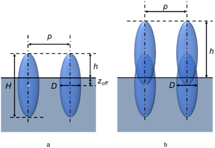 | ||
| Fig. 1 Parameters of the voxel array. (a) Monolayer or so-called single-voxel array; (b) accumulative or so-called multivoxel array. | ||
Each of the substrates with a 50 × 50 μm2 surface used for the final SERS measurements in this work took approximately 2 hours to fabricate because of the large amount of fine piezo movements. Further comparisons of the techniques and their advantages and disadvantages are described below in the manuscript.
After the 2PP process was completed, the unpolymerized material was washed away during the development process. The fabricated substrates were in the next step coated with 25 nm gold using a JEOL JFC-2300HR high-resolution coater, a device that allows the creation of thin layers of material over substrates accompanied by the FC-TM20 thickness controller to control the amount of material. The thickness of the coating was chosen based on the fact that the gold penetration depth at a wavelength of 785 nm corresponds to ∼24 nm.25
Next, a Dimension 3100 System Atomic Force Microscope (AFM) from Brüker and a Scanning Electron Microscope (SEM) S-4800 from Hitachi High-Tech were used to characterize the structures. For the AFM measurements, a soft tapping mode in the air was used. The scan was performed within the central region of the substrate, corresponding to an area of 10 × 10 μm2. The center of the substrate was defined by considering an equal distance from the edges of the substrate. Moreover, the gold coating layer's thickness, i.e. 25 nm, is also verified with AFM by taking the non-coated surface of the glass substrate as a reference.
Finally, Raman measurements were performed using a commercial InVia confocal Raman system (Renishaw). For this study, a 785 nm excitation laser was used. A charge-coupled device (CCD) camera was used to capture the Raman spectra. The system was described in detail in ref. 26.
2.3 Numerical simulations
For nanostructure simulations, the Ansys Lumerical software, particularly the Finite-Difference Time-Domain (FDTD) solver, is used.27 This approach enables the design and optimization of the geometry, size, shape, and arrangement of nanostructures on SERS substrates.To match the experimental conditions in the simulations, a layer of gold coating of 25 nm is applied on top of the nanostructures, corresponding to the gold layer applied during fabrication. With FDTD simulations, the localized plasmon resonance (Eloc) with high intensity, or the so-called “hotspots”, induced by the original electromagnetic field (E0), can be calculated.28 The simulated enhancement factor or single molecular enhancement factor (SMEF) can be estimated as SMEF ≅ |Eloc(wR)|4/|E0(wR)|4. The highest enhancement factor (EFmax) for a nanostructure is attained when the sample molecule is precisely positioned on the surface and exhibits the highest local electromagnetic field (Emax). FDTD simulations were carried out using the actual shapes of the fabricated nanostructures, as characterized by AFM measurements. This allowed us to benchmark the SERS enhancement performance against the nominal shape model, as detailed in Section 3.2.
2.4 Measurement and calculations
As mentioned above, an InVia confocal Raman microscope was used to perform the SERS measurements. A microwell was placed on top of the fused silica substrate by placing the 50 × 50 μm2 large SERS structures in the middle of the bottom of the well. The latter has 5.7 × 6.1 × 6.8 mm3 dimensions. To ensure that the droplet of the solution homogeneously covered the bottom of the well, including the SERS substrate, 8 μL of low-concentration BPE-ethanol solution was added for each measurement. Ethanol is a volatile liquid that evaporates after a few minutes in the air. This volume of solution corresponds to a height of 230 μm inside the microwell, which is sufficient to cover the nanostructures with a height of only several micrometers. Note that the solutions measured here are made of the target molecules mixed with ethanol, meaning that after some time, the latter evaporates and only the molecules of BPE remain on the SERS substrate.Raman mapping of a 30 × 30 μm2 surface with a 2 μm scan step, resulting in 81 spectra, was performed in the central area of each substrate to characterize their performance and reproducibility. Three substrates were measured for each type to calculate the map-to-map variation. This variation is defined as the standard deviation of the respective characteristic peak. Asymmetric Least Squares (ALS) subtracts the baselines from the spectra.29 This step ensured that any variation in intensity was not due to the background fluorescence. Subsequently, we calculated the standard deviation (STD), enhancement factor (EF), and limit of detection (LOD) for each of the most prominent characteristic peaks of the analyte, that is, 1198 and 1606 cm−1. First, mapping was performed multiple times without the analyte. These measurements were used to analyze the noise of the measurements. An acquisition with 0.1% laser power corresponding to 0.46 mW for 785 nm excitation was recorded for 0.5 s per spectrum using 1200 lines per mm grating and 20× long distance objective in standard confocality mode. The laser spot size corresponded to 2.5 μm. An excitation wavelength of 785 nm was selected because it is the most widely used wavelength in biosensing applications.1
These measurements were used to calculate the STD necessary for LOD calculations. For further experiments, when different concentrations of BPE were added, only one measurement was recorded per map, creating a calibration plot per Raman shift of interest over the acquired map. The linear part of the calibration curve was used to calculate LOD = 3.3σ/S, where σ is the STD calculated at the Raman shift of interest without the analyte, and S is the slope of the linear part of the calibration curve. Furthermore, the most widely used definition of SERS EF, that is, EF = (ISERS/NSERS)/(INR/NNR), was used to study the enhancement capabilities of the substrates at the Raman shifts of interest.12,28ISERS is the SERS peak intensity, NSERS is the number of molecules on the surface contributing to the SERS signal, INR is the same peak intensity in the spontaneous Raman spectrum, and NNR is the number of molecules in the laser collection volume when measuring spontaneous Raman. The area of the beam spot was calculated using the airy-disk formula to determine NSERS assuming a uniform molecular distribution. The INR was measured in a homogeneous solution. Ethanol does not emit fluorescence with near-infrared excitation, nor does it overlap the Raman peaks with the analytes. Therefore, the main contribution to INR is from the homogeneously distributed molecules in the collection volume, calculated as the area of the beam spot multiplied by the confocality height. The full width at half-maximum of the 520 cm−1 peak of the silicon target in a height scan was taken as the confocality height.
3. Results and discussion
Recently published FDTD simulations21 show a parametric sweep varying the height of the structures and the distance between them. This study aimed to provide an in-depth understanding of the optimal structural characteristics of nanostructures. Hence a heatmap of the electric field amplitude between two neighboring pillars in the case of different combinations of these nano-printing parameters was created and analyzed. In the simulations, the diameter of the single voxel was chosen at 250 nm, corresponding to the experimental dimensions of the smallest unit of the photoresin volume polymerized with a single laser spot illumination. Furthermore, taking into account the NanoScribe system's specifications, a pitch between 300 and 900 nm, and a height varying between 200 nm and 1.2 μm was chosen. According to the simulation's outcome, a pitch near 300 nm consistently induced the highest enhancement independent of the height of the array. In this section, we present the results of the characterization of the nanopillar arrays made with both the single-voxel and multivoxel approaches and obeying the abovementioned dimensions.3.1 Characterization and optimization of nanostructures
To perform 2PP printing with the Nanoscribe Photonic Professional GT+ system, the structures were first designed using DeScribe. A sweep of the nanostructure parameters, like in the simulations, was performed to obtain the most optimal fabrication conditions.For single-layer voxel fabrication, the exposure laser power of the nanoprinter was kept constant at 24 mW to obtain optimal voxel shapes.30 The heights of the structures and pitch were varied. Based on the FDTD simulation results, the best enhancement was achieved with voxel arrays with an aspect ratio larger than 1.5. Height at 100, 300, 400, and 600 nm were designed, while the pitch values were chosen as 300, 400, and 600 nm. Several combinations of aspect ratios and pitch values were fabricated as provided in Table 1 in ESI.† The structures were characterized by AFM and SEM. Table 1 in ESI† also summarizes the measurement results. The designed height and pitch listed in Table 1 in ESI,† correspond to the parameters used in the DeScribe code. The measurement results show good agreement between the designed and obtained pitch values. In most cases, the fabrication error is less than 6% in the horizontal (XZ) and vertical (YZ) cross-sections of the measured 3D structures. However, in a single substrate, the difference between the pitch values in XZ and YZ was large, reaching a deviation of up to 20% from the designed values. Changes in height accompanied these deviations in pitch values. The voxel diameters were also smaller following the aspect ratio for shorter structures with heights of 100 or 300 nm. This yields a well-separated nanostructure fabrication, which in turn allows a uniform distribution of a single-voxel-based array. However, when the height of the structures is between 400 and 600 nm, and the pitch varies between 300 and 400 nm, the structures attach to each other, creating attached single-voxel non-uniform arrays, as shown in Fig. 2(a) and (b). Such behavior also affects height uniformity because the distance between the peak of the nanostructure and the point where it is clearly separated from the neighboring nanostructure differs in the XZ and YZ directions.
| # | Name | E max 2/E02 | EFmax |
|---|---|---|---|
| 1 | Hamamatsu | 287.5 | 8.27 × 10⁴ |
| 2 | Attached single-voxel (Fig. 2(a)) | 431.1 | 1.86 × 10⁵ |
| 3 | Half uniform-half collapsed single-voxel (Fig. 5(a)) | 323.9 | 1.05 × 10⁵ |
| 4 | Collapsed single-voxel (Fig. 2(c)) | 921.3 | 8.49 × 10⁵ |
| 5 | Multivoxel uniform (Fig. 4(b)) | 446.7 | 2.01 × 10⁴ |
| 6 | Multivoxel collapsed (Fig. 4(d)) | 1349.2 | 1.82 × 10⁶ |
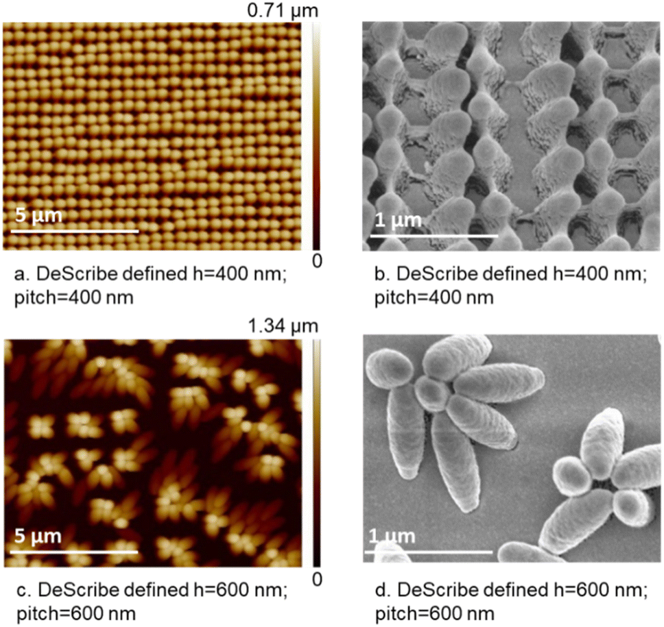 | ||
| Fig. 2 AFM (a and c) and SEM (b and d) images of nanostructures fabricated with the single-voxel-based approach. Parameters here are the designed values given in Table 1 in ESI.† | ||
By utilizing the 2PP technology it is possible to fabricate structures down to a height of 75 ± 30 nm, resulting in an aspect ratio of ≈0.3. According to our earlier work,21 it has been suggested that the best enhancement factors are achieved with an aspect ratio of >1.5. Hence, the structures with smaller aspect ratios have not been further investigated. Nevertheless, these structures can be used in other applications if a combination of these parameters is desired.
Finally, under certain conditions, the voxels collapsed on each other, as shown in Fig. 2(c) and (d). So-called collapsed single-voxel structures occur when the voxel's height and pitch are large. The voxels were not strong enough to stand steady when their diameter close to the glass substrate was much smaller than the entire voxel itself, as shown in Fig. 2(d). In this case, the parameters of the individual nanostructures do not play a role in the SERS behavior because the assemblies of collapsed voxels create new geometries that are difficult to control in advance. Collapsing is highly dependent on the post-polymerization process during the development of structures. The samples were manually immersed into the developing solution, and depending on the speed and angle of immersion, different forces affect the voxels differently. In some cases, one-half of the structures collapse and the other half stands steadily on the same substrate, resulting in a so-called half uniform-half collapsed single-voxel array, as shown in Fig. 5(a). The development process requires further improvement to achieve controlled and reproducible fabrication of collapsed structures. Nevertheless, after coating the substrates with gold, no further structural changes are observed.
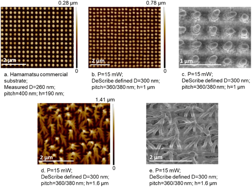
Further investigations were focused on increasing the aspect ratio of the nanopillars while aiming for a more uniform distribution of the latter. By overcoming the trade-off between the diameter and height of a single voxel, 2PP fabrication configurations were set such that a nanostructure was constructed using smaller voxels stacked on top of each other, as illustrated in Fig. 1(b). The laser power variation was studied in search of the smallest reproducible voxel fabrication regime. Fig. 3 shows the influence of the fabrication settings and structural specifications on the printing result. P is the laser power and D is the diameter of a single voxel. The power values vary from 12 mW to 16.5 mW. Arrays of structures with diameters of 250, 300, and 400 nm and pitches of 300, 350, and 380 nm were designed using DeScribe. As seen in Fig. 3(a) and (b), respectively, a laser power of 12 mW is barely sufficient to polymerize structures with the smallest diameters and hardly create nanostructures with the largest diameters. On the other hand, with 16.5 mW power, the diameter of the structures gets so large that it results in connections between the structures, as shown in Fig. 3(e). Moreover, the pitches in the XZ and YZ directions are different. This is because the laser beam is not an ideal Gaussian. Hence, the polymerization cross-section is not an ideal circle, especially noticeable at high powers. This causes pitch variation, indicating the need to design arrays of nanostructures with different pitches in the vertical and horizontal directions. Implementing this strategy, the fabrication of arrays of homogeneously distributed structures at 14.25 and 15 mW laser powers as shown in Fig. 3(c) and (d), respectively, was successful. The fabrication of uniform nanostructure arrays was comparable to that reported in the literature.20 At the same time, the AFM measurements of different structures demonstrate that for 14.25 mW power, the height of the structures is less than that in the case of 15 mW. This can be explained by the fact that when the laser power increased, the dimensions of a single voxel also increased, making the resulting structure to be larger. Note, that the diameter of the structures corresponds to the diameter of a single voxel, as indicated in Fig. 1.
 | ||
| Fig. 3 AFM images of nanostructures fabricated with the multivoxel-based approach. (a and b) Correspond to the same lowest laser power with different height and pitch values. (c and d) Differ only in power values, and (e) corresponds to the highest applied laser power. Parameters here are the designed values given in Table 2 in ESI.† | ||
Table 2 in ESI† summarizes the outcome of the AFM measurements for different combinations of parameters for the nanostructures when the height in DeScribe is set equal to 1 μm corresponding to 4 voxels on top of each other. Using these results, one can determine the best fabrication parameters to further improve the high aspect ratio nanofabrication. A laser power of 15 mW, pitches in the 360–380 nm range, and a voxel diameter of 300 nm were selected for fabricating multilayer voxel-based nanostructure arrays at a height of 1 μm. AFM measurements of the multivoxel uniform substrates with the mentioned parameters reveal that the printed nanostructures exhibit lateral characteristics like those of the SERS substrate from Hamamatsu shown in Fig. 4(a). The pitch was 400 nm, and the diameter of the structures was 260 nm for both substrates, while the 2PP-fabricated nanostructures have a height of 460 nm, and the Hamamatsu ones have a height of 190 nm.
| # | Name | Mean EF | Max EF | EF error |
|---|---|---|---|---|
| 1 | Hamamatsu | 1.13 × 10⁵ | 4.33 × 10⁵ | 1.09 × 10⁵ |
| 2 | Attached single-voxel | 8.59 × 10⁵ | 2.26 × 10⁶ | 2.21 × 10⁵ |
| 3 | Half uniform-half collapsed single-voxel | 4.06 × 10⁵ | 9.07 × 10⁵ | 1.53 × 10⁵ |
| 4 | Collapsed single-voxel | 1.08 × 10⁶ | 1.80 × 10⁶ | 2.17 × 10⁵ |
| 5 | Multivoxel uniform | 2.76 × 10⁵ | 7.71 × 10⁵ | 1.15 × 10⁵ |
| 6 | Multivoxel collapsed | 3.82 × 10⁵ | 1.02 × 10⁶ | 1.45 × 10⁵ |
 | ||
| Fig. 4 (a) AFM image of Hamamatsu gold-coated dot array. (b and d) AFM and (c and e) SEM images of 2PP-fabricated nanostructures. The height of the structures is designed to be (b and c) 1 μm and (d and e) 1.6 μm. The pitch in XZ and YZ directions is respectively 360 and 380 nm, with a 300 nm voxel diameter. | ||
When the nanostructures' height is further increased while keeping their diameter the same, they tend to collapse onto each other, creating multivoxel collapsed arrays. However, the difference from the previously discussed case (see Fig. 2(e)) is the high aspect ratio of the individual structures. Here, the aspect ratio was calculated as ≈4, whereas in the first case, it was ≈1.5. Moreover, the distribution of the collapsed structures over the array is more homogenous and controlled in this case, as shown in Fig. 4(d) and (e).
Note that the fabrication of all optimized structures was repeated more than 10 times. Each fabrication batch contained three structures with the same set of parameters. Most of the time two out of three had similar characteristics. One of the possible reasons for such behavior, as mentioned earlier, is the development process which requires further improvement.
3.2 FDTD models of the AFM-measured structures
Next, simulations in Lumerical were performed to estimate the enhancement factor and SERS performance of the fabricated nanostructures. The surface profile data for all the printed nanostructure arrays obtained through AFM were converted into stereolithographic files (*. stl). These files were used to construct FDTD models to assess their electromagnetic performance under laser excitation. Table 1 presents the simulated EFs of the SERS substrates. Based on the AFM data-based FDTD model, the multivoxel-based collapsed structure exhibited the highest EF, reaching 1.82 × 10⁶. Conversely, the lowest EF was observed in a multivoxel-based uniform structure, measuring 2.01 × 10⁴. Most of the fabricated SERS substrates displayed EFs ranging from to 104–106. For reference, the Hamamatsu SERS substrate possesses an EF of 8.27 × 10⁴.These FDTD simulations based on AFM data offer significant insights into the enhancement factors of SERS substrates, particularly highlighting the distribution of electromagnetic resonance (hotspots) on SERS substrate surfaces. Fig. 5(a) illustrates the AFM-measured profile of the structure printed with a pitch of 600 nm, diameter of 490 nm, and height of 850 nm. As mentioned above, some voxel structures collapsed, whereas others remained intact. This structure is particularly interesting for FDTD simulations, hence in a single substrate one can observe hotspot distribution for both uniform and collapsed structures. The electromagnetic field distribution on the surface of the fabricated SERS substrate is shown in Fig. 5(b). Hotspots were uniformly distributed on the tips and between adjacent voxels when the voxels were intact. However, the hotspots exhibited a higher overall field intensity in the collapsed region, although with a more random distribution. It is important to note that the dimensional information underneath the collapsed voxels was not recorded owing to the AFM measurement principle. As a result, the enhancement within this region was not presented in the simulation based on the AFM data-based model. This can also explain possible differences between simulated and experimental results for the enhancement factor.
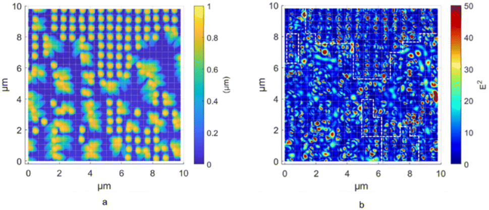 | ||
| Fig. 5 AFM image (a) and FDTD simulation (b) of the single-voxel-based array with structures of 600 nm pitch, 490 nm diameter, and 850 nm height. Color bars represent (a) the height of the structures and (b) the electromagnetic field intensity. | ||
3.3 SERS performance analysis
After analyzing the morphology of the SERS substrates using microscopy and estimating their EF through finite-difference time-domain (FDTD) simulations, SERS measurements were conducted to evaluate and characterize their enhancement performance. BPE was measured as the performance analyte to estimate the LOD and experimental EF of the structures. As mentioned above, Raman mapping was performed to investigate the spatial characteristics of the substrates. A spatial average of 256 spectra over a 32 μm window in the middle of the selected substrates is presented in Fig. 6(a). The two strongest peaks of the BPE spectra, 1198 and 1606 cm−1, were considered for the reported results.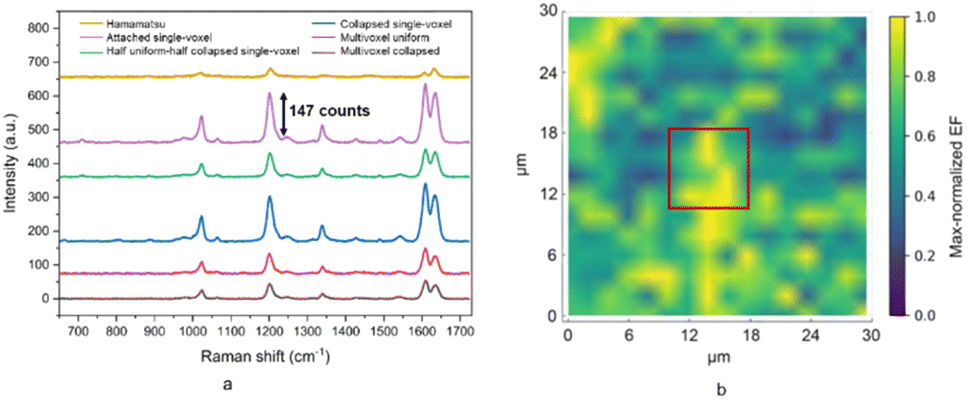 | ||
| Fig. 6 (a) Spectrum of BPE using above mentioned SERS substrates, compared to a Hamamatsu substrate. The spectra are averaged over a map of 256 spectra, and the baseline is corrected using the intelligent polynomial baseline correction of Renishaw's WiRE software. (b) 30 μm × 30 μm experimental enhancement factor heatmap (2 μm resolution) max-normalized to examine collapsed vs. uniform nanostructures for the 1606 cm−1 peak of 2.5 μM BPE. The red square indicates the surface area corresponding to the AFM-measured region. On the color bar, 0 corresponds to 1.02 × 10⁵ and 1 to 7.36 × 10⁵, respectively. | ||
The EF can explain the ability of the substrates to enhance the Raman signal. A higher EF indicates a stronger signal and potentially a higher sensitivity, that is, a lower LOD. Fig. 6(b) shows a heatmap of the max-normalized experimental enhancement factor, focusing on comparing collapsed and uniform nanostructures for the 1606 cm−1 peak of 2.5 μM BPE. It is important to note that Fig. 6(b) has an approximately three times larger window compared to Fig. 5(a) and (b) because Raman mapping has been performed for a larger surface area. The area inside the red square in Fig. 6(b) corresponds to the AFM-measured surface and one can appreciate the disparities in EF values between regions where the structures collapsed versus uniform, with the latter having a relatively lower EF and a more uniform distribution. These observations were in good agreement with the simulation results shown in Fig. 5(b).
The mean and maximum EF over the measured map for the selected structures are shown in Fig. 7(a) and (b), respectively, and are summarized in Table 2. It can be seen how the 2PP-printed substrates perform better than the Hamamatsu samples for both the mean and maximum EF because of the higher aspect ratio of the structures. The fabricated substrates had a higher aspect ratio and, consequently, a higher hotspot density. Moreover, the attached single-voxel and collapsed single-voxel structures had the best performance, 2.26 × 10⁶ and 1.80 × 10⁶, respectively. This can be attributed to the density of high-quality hotspots created by these structures owing to their relatively narrow gaps. Furthermore, the errors reported in Table 2 highlight the microscale spatial variations in enhancement. These errors are comparable to those observed in Hamamatsu's commercial SERS substrate, which is known for its reproducibility and structural uniformity.10 These microscale variations can be reduced using larger laser beam spot sizes in Raman measurements. Differences between simulated and measured EF values can be caused by the analyte's concentration distribution on the substrates' surface, depending on where the BPE molecules remain after the ethanol evaporates in the area between two neighboring structures. This directly affects the Raman scattering, which is not considered in the numerical simulations. Nevertheless, good agreement between the order of magnitude is achieved.
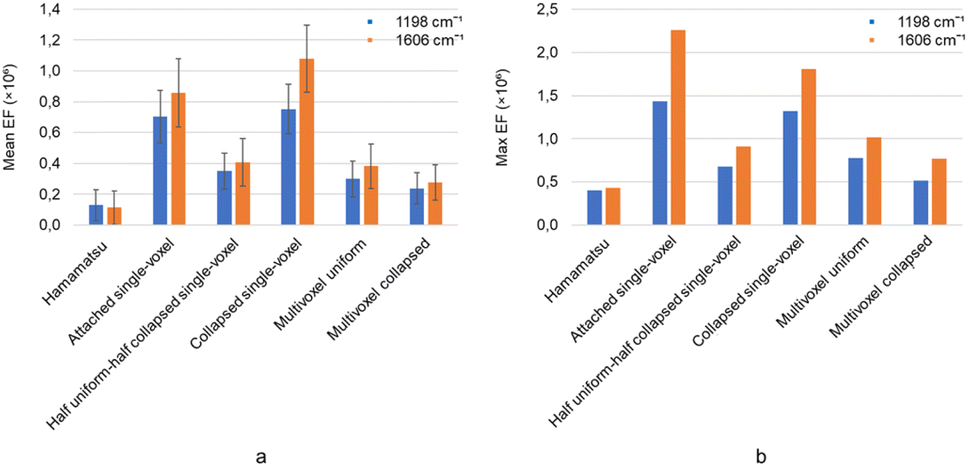 | ||
| Fig. 7 The mean (a) and maximum (b) enhancement factor over the measured map of the SERS substrates for 1.5 μM BPE's peaks of interest. The error bars show the map-to-map variation of the EF values for the selected peak, while the mean and maximum values are calculated over each map. | ||
Furthermore, the relative STD (RSD) of EF at 1606 cm−1 over the map which includes 81 points, for attached single-voxel and collapsed single-voxel structures was 26% and 20%, respectively. These spatial variations were partly due to the proximity of the analyte concentration, i.e., 1.5 μM, to the LOD of the substrates, as shown in Fig. 8 and Table 3.
 | ||
| Fig. 8 The mean (a) and minimum (b) LOD over the measured map of the SERS substrates for BPE's peaks of interest in spectra averaged over each map. The bars, i.e. mean values, are calculated over multiple measured maps. The error bars show the map-to-map variation of the LOD. | ||
| # | Name | Mean LOD (μM) | Minimum LOD (μM) | Error (μM) |
|---|---|---|---|---|
| 1 | Hamamatsu | 5.42 | 2.63 | 1.75 |
| 2 | Attached single-voxel | 0.82 | 0.21 | 0.35 |
| 3 | Half uniform-half collapsed single-voxel | 1.52 | 0.22 | 0.69 |
| 4 | Collapsed single-voxel | 1.20 | 0.17 | 0.64 |
| 5 | Multivoxel uniform | 1.83 | 0.42 | 0.73 |
| 6 | Multivoxel collapsed | 1.65 | 0.30 | 0.75 |
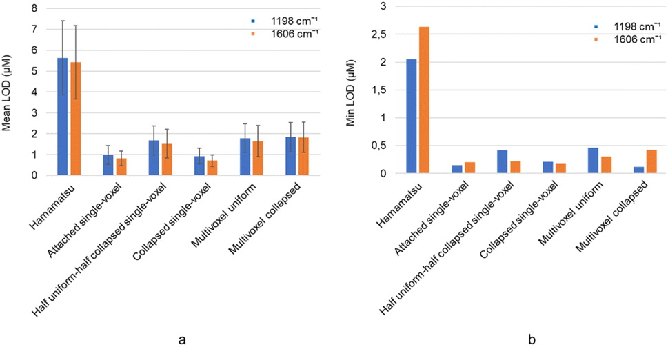
The LOD values depicted in Fig. 8 and summarized in Table 3 adhere to the principle that higher enhancement correlates with higher sensitivity, meaning a lower LOD. An example calibration plot for a collapsed single-voxel substrate is presented in Fig. 2 in ESI.† Moreover, Fig. 3 in ESI† presents spectra corresponding to some of the concentrations in the calibration plot. The best sensitivity was found for the attached single-voxel and collapsed single-voxel structures, with a minimum LOD of 210 and 170 nM, respectively, at 1606 cm−1. This was approximately 10-fold higher than Hamamatsu's LOD under the same measurement conditions.
Table 4 summarizes the comparison between the commonly used commercial SERS substrates10 and the 2PP-fabricated ones. The substrates developed in this work exhibit enhancement factors of the same order of magnitude as the commercial substrates, while also demonstrating a highly uniform distribution of nanostructure arrays, thus yielding reproducible signal over the whole SERS substrate. The unique property of this technique is the possibility to control the fabrication of the individual nanopillars. Noteworthy, one of the most important advantages of these substrates is that the cycle of fabrication is short, i.e. from design to fabrication and prototyping takes a maximum of 2 hours. This is thanks to the fact that the direct laser writing technique does not require a mold or additional chemical treatments, besides washing away unpolymerized residual material after the fabrication process.
| SERS substrate | Fabrication technique | Structural order | Substrate uniformity | Max aspect ratio | Max EF (order of magnitude) |
|---|---|---|---|---|---|
| Hamamatsu | Nanoimprinting | Dot array | Uniform | 0.4 | 105 |
| Silmeco Au | Reactive ion-etching | Nanopillars | Random | 5.4 | 107 |
| Uniform distributed nanopillars | Two-photon polymerization | Nanopillar array | Uniform | 1.5 | 105 |
| Collapsed nanopillars | Two-photon polymerization | Bent nanopillar array | Uniform collapsed | 4 | 106 |
Conclusions
This study successfully demonstrates the potential of two-photon polymerization-based nano-printing as a rapid, cost-efficient method for fabricating high-performance SERS substrates. Through FDTD simulations, the optimal parameters for the nanopillar height and pitch are determined, guiding the fabrication process to achieve structures with enhanced electric field intensities. Two different SERS fabrication approaches are studied namely single-voxel and multivoxel fabrication methods. 2PP-based highly controlled direct laser writing technology enables the reproducible fabrication of uniformly distributed nanopillar arrays reaching aspect ratios as high as 4 with a multilayer voxel-based printing approach. This process takes approximately 2 hours. Single-voxel-based nanostructure arrays can be fabricated in less than a minute creating structures with an aspect ratio of approximately 1.5. Characterization using AFM and SEM confirmed that the fabricated structures closely matched the pre-set parameters of the nano-printer. However, deviations were observed at higher aspect ratios, particularly with the single-voxel method. FDTD simulations based on AFM-measured structures indicated that the collapsed multivoxel structures provided the highest enhancement factors, reaching up to 1.82 × 10⁶. Experimental SERS measurements with BPE analyte supported these findings, showing that the 2PP-fabricated collapsed multivoxel structures show up to 1.02 × 10⁶ enhancement factor. The collapsed single-voxel substrates exhibited a maximum EF of 1.80 × 10⁶, with an LOD as low as 0.17 μM, outperforming commercial Hamamatsu substrates in both the 1.13 × 10⁵ enhancement factor and limit of detection at 2.63 μM, respectively. These results, combined with the uniformity of the nanostructures' distribution over the entire surface of the substrate and the high aspect ratio of the individual nanopillars, put the SERS substrates developed in this work in line with the best-performing commercial substrates such as the ones from Hamamatsu and Silmeco.This 2PP fabrication process opens the possibility to further improve the fast prototyping of nanostructures that can be customized for SERS applications. The ability to rapidly prototype and control structural parameters at the nanoscale is demonstrated to improve the SERS performance. Moreover, using metal nanoparticles as additives to the polymer during the fabrication process can pave the way for further enhancement of hot spot concentrations over the surface of the substrate thus increasing the sensitivity of the latter.31 Future research should focus on optimizing the post-polymerization process to further enhance structural uniformity at even higher aspect ratios, as well as exploring novel applications for these custom-fabricated nanostructures.
Data availability
As required, data, such as Raman spectra, AFM and SEM data used in this work can be found in a shared drive https://drive.google.com/drive/folders/1hJrrdBCtkvH6gyBVpNEwVhcSegVNA2Bx?usp=drive_link.Author contributions
Tatevik Chalyan: conceptualization, methodology, investigation, visualization, AFM, and Raman data acquisition, AFM data curation, revising, writing – original draft. Mehdi Feizpour: conceptualization, methodology, experimental data curation, formal analysis, visualization, revising, writing – original draft. Qing Liu: conceptualization, methodology, numerical simulations, visualization, writing – original draft. Koen Vanmol: methodology, nanofabrication software, revising, funding acquisition. Núria Solerdelcoll: nanofabrication software. Gen Takebe: SEM data acquisition. Heidi Ottevaere: supervision, revising, funding acquisition. Hugo Thienpont: funding acquisition.Conflicts of interest
There are no conflicts to declare.Acknowledgements
This work was supported in part by FWO (G029919N, 12E2923N), the Methusalem program of the Flemish government and Hercules foundations, and the Scientific Research Council (OZR) of the Vrije Universiteit Brussel (VUB).References
- K. Eberhardt, C. Stiebing, C. Matthäus, M. Schmitt and J. Popp, Expert Rev. Mol. Diagn., 2015, 15, 773–787 CrossRef CAS.
- M. K. Shukla, P. Wilkes, N. Bargary, K. Meagher, D. Khamar, D. Bailey and S. P. Hudson, Spectrochim. Acta, Part A, 2023, 299, 122872 CrossRef CAS PubMed.
- A. Balčytis, Y. Nishijima, S. Krishnamoorthy, A. Kuchmizhak, P. R. Stoddart, R. Petruškevičius and S. Juodkazis, Adv. Opt. Mater., 2018, 6, 1800292 CrossRef.
- M. Shao, C. Ji, J. Tan, B. Du, X. Zhao, J. Yu, B. Man, K. Xu, C. Zhang and Z. Li, Opto-Electron. Adv., 2023, 6, 230094 CAS.
- A. Elkady, O. M. Helal, M. A. Abdalla and M. F. Hagag, in 2024 14th International Conference on Electrical Engineering (ICEENG), 2024, pp. 72–77 Search PubMed.
- L. Yu, Q. Zheng, H. Wang, C. Liu, X. Huang and Y. Xiao, Anal. Chem., 2020, 92(1), 1402–1408 CrossRef CAS PubMed.
- Z. Guo, Y. Zheng, L. Yin, S. Xue, L. Ma, R. Zhou, H. R. El-Seedi, Y. Zhang, N. Yosri, H. Jayan and X. Zou, Sens. Actuators, B, 2024, 404, 135303 CrossRef CAS.
- K. Yuan, B. Jurado-Sánchez and A. Escarpa, J. Nanobiotechnol., 2022, 20, 537 CrossRef CAS PubMed.
- SERS biosensing of sickle cell hemoglobin from normal hemoglobin, https://www.spiedigitallibrary.org/conference-proceedings-of-spie/12654/2675806/SERS-biosensing-of-sickle-cell-hemoglobin-from-normal-hemoglobin/10.1117/12.2675806.short, accessed 10 July 2024.
- M. Feizpour, Q. Liu, T. V. der Donck, H. Thienpont, W. Meulebroeck and H. Ottevaere, J. Phys.: Photonics, 2024, 6, 025002 Search PubMed.
- J12853 – HAMAMATSU, Substrate for the electronics industry J12853, https://www.directindustry.com/prod/hamamatsu/product-13622-2365936.html, accessed 8 October 2023.
- M. S. Schmidt, J. Hübner and A. Boisen, Adv. Mater., 2012, 24, OP11–OP18 CAS.
- L. Mehrvar, M. Sadeghipari, S. H. Tavassoli, S. Mohajerzadeh and M. Fathipour, Sci. Rep., 2017, 7, 12106 CrossRef CAS PubMed.
- S.-C. Luo, K. Sivashanmugan, J.-D. Liao, C.-K. Yao and H.-C. Peng, Biosens. Bioelectron., 2014, 61, 232–240 CrossRef CAS.
- K. Stokes, K. Clark, D. Odetade, M. Hardy and P. Goldberg Oppenheimer, Discover Nano, 2023, 18, 153 CrossRef CAS PubMed.
- S. Maruo, O. Nakamura and S. Kawata, Opt Lett., 1997, 22, 132–134 CrossRef CAS PubMed.
- M. Farsari and B. N. Chichkov, Nat. Photonics, 2009, 3, 450–452 CrossRef CAS.
- Q. Liu, K. Vanmol, S. Lycke, J. V. Erps, P. Vandenabeele, H. Thienpont and H. Ottevaere, RSC Adv., 2020, 10, 14274–14282 RSC.
- T. Chalyan, Q. Liu, M. Feizpour, H. Thienpont and H. Ottevaere, in Optica Advanced Photonics Congress 2022, paper JTu2A.49, Optica Publishing Group, 2022 Search PubMed.
- J. A. Kim, D. J. Wales, A. J. Thompson and G.-Z. Yang, Adv. Opt. Mater., 2020, 8, 1901934 CrossRef CAS.
- Q. Liu, T. Chalyan, M. Feizpour and H. Ottevaere, inNanophotonics X, SPIE, 2024, vol. 12991, pp. 227–231 Search PubMed.
- X. Zhou, Y. Hou and J. Lin, AIP Adv., 2015, 5, 030701 CrossRef.
- NanoScribe, Nanoscribe photoresins specifically designed for Two-Photon Polymerization, https://www.nanoscribe.com/en/products/ip-photoresins/, accessed 25 September 2023.
- Y. Zhou, Y. Kong, S. Kundu, J. D. Cirillo and H. Liang, J. Nanobiotechnol., 2012, 10, 19 CrossRef CAS.
- M. O. Sallam, G. A. E. Vandenbosch, G. Gielen and E. A. Soliman, Opt. Express, 2014, 22, 22388–22402 CrossRef PubMed.
- T. Chalyan, I. Magnus, M. Konstantaki, S. Pissadakis, Z. Diamantakis, H. Thienpont and H. Ottevaere, Biosensors, 2022, 12, 227 CrossRef CAS PubMed.
- Ansys Lumerical, Photonics Simulation Software, https://www.ansys.com/products/photonics, accessed 5 October 2023 Search PubMed.
- E. C. Le Ru, E. Blackie, M. Meyer and P. G. Etchegoin, J. Phys. Chem. C, 2007, 111, 13794–13803 CrossRef CAS.
- P. H. C. Eilers, Anal. Chem., 2004, 76, 404–411 CrossRef CAS PubMed.
- A.-I. Bunea, N. del Castillo Iniesta, A. Droumpali, A. E. Wetzel, E. Engay and R. Taboryski, Micro, 2021, 1, 164–180 CrossRef.
- N. I. Kilic, G. M. Saladino, S. Johansson, R. Shen, C. McDorman, M. S. Toprak and S. Johansson, ACS Appl. Mater. Interfaces, 2023, 15, 49794–49804 CrossRef CAS.
Footnote |
| † Electronic supplementary information (ESI) available. See DOI: https://doi.org/10.1039/d4na00742e |
| This journal is © The Royal Society of Chemistry 2025 |