
 Open Access Article
 This Open Access Article is licensed under a Creative Commons Attribution-Non Commercial 3.0 Unported Licence
Selective modal excitation in a multimode nanoslit by interference of surface plasmon waves
Marcos Valeroab,
Luis-Angel Mayoral-Astorgab,
Howard Northfieldb,
Hyung Woo Choib,
Israel De Leonbc,
Mallar Ray *a and
Pierre Berini*bde
*a and
Pierre Berini*bde
aSchool of Engineering and Sciences, Tecnológico de Monterrey, Monterrey, Nuevo León 64849, Mexico. E-mail: mallar.ray@tec.mx
bSchool of Electrical Engineering and Computer Science, University of Ottawa, Ottawa, Ontario K1N 6N5, Canada. E-mail: pberini@uottawa.ca
cASML Netherlands B.V., De Run 6501, 5504 DR Veldhoven, The Netherlands
dDepartment of Physics, University of Ottawa, Ottawa, Ontario K1N 6N5, Canada
eNexus for Quantum Technologies Institute, University of Ottawa, Ottawa, Ontario K1N 6N5, Canada
First published on 9th January 2025
Abstract
Interference of surface plasmons has been widely utilized in optical metrology for applications such as high-precision sensing. In this paper, we introduce a surface plasmon interferometer with the potential to be arranged in arrays for parallel multiplexing applications. The interferometer features two grating couplers that excite surface plasmon polariton (SPP) waves traveling along a gold–air interface before converging at a gold nanoslit where they interfere. A key innovation lies in the ability to tune the interference pattern by altering the geometrical properties of the gold nanoslit such that one, two or more resonance modes are supported in the nanoslit. Our experimental results validate the approach of our design and modelling process, demonstrating the potential to fine-tune geometrical parameters such as grating coupler pitch, depth, duty cycle, and nanoslit dimensions to alter the transmitted radiation pattern and the transmittance. We demonstrate the ability of a grating coupler to induce focusing of SPP waves to an arbitrary location on chip by illuminating with a converging Gaussian beam. Additionally, we observed far-field interference patterns linked to the multimodal operation of the nanoslit.
1 Introduction
Surface plasmon polariton (SPP) waves are electromagnetic waves that travel along the interface between a metal and a dielectric.1–4 These waves arise from the coupling of the electromagnetic field with the collective oscillations of the metal's conduction electrons, resulting in a highly confined wave that propagates with enhanced fields and high sensitivity to changes in the local refractive index of the dielectric.5–7 Similar to light waves, coherent SPP waves can interfere to produce an interference pattern.8,9 A common configuration for harnessing the interference of SPP waves is the Mach–Zehnder interferometer.10–19 This configuration splits the SPP wave into two paths, typically a reference arm and a sensing arm, before recombining them to generate interference. The Mach–Zehnder interferometer is widely used because it allows for precise control of the optical phase difference between the two arms, enabling sensitive phase-based detection of changes in the refractive index, which is crucial for applications such as biosensing and environmental monitoring.Several Mach–Zehnder SPP interferometers have been proposed; however, individual interferometers are generally challenging to arrange closely together in compact configurations. This limitation is particularly troublesome for multiplexing applications, as in biosensors where the detection of multiple biomarkers simultaneously is desirable.20–24 To address this, we propose an interferometer structure that allows for perpendicular interrogation by utilizing two gold grating couplers, a gold propagation surface acting as interferometer arms, and a nanoslit acting as a combiner. This simple yet effective configuration enables the system to be arranged both vertically and horizontally, making it possible to array multiple interferometers close together for multiplexing capabilities.
A key component of our device is the grating coupler, which is used to efficiently excite SPP waves on the metal–dielectric interface. Grating couplers are structures with periodic variations that match the momentum of incident light to that of the SPP waves, allowing the light to couple into the plasmonic mode.25–32 This method is widely recognized as one of the most effective ways to excite SPPs due to its ability to achieve high coupling efficiency and its compatibility with various optical setups. Numerous devices in the literature utilize grating couplers for SPP excitation. The design mechanism of the grating couplers in our proposed configuration is similar to those established methods.
The second key element of our device is the gold nanoslit, which serves as the interferometric combiner for SPP waves. Gold nanoslits have been primarily used to filter spectral components of light and support extraordinary optical transmission.33–36 The gold nanoslit in our case consists of a narrow gap milled into the gold film, capable of supporting one, two or more resonance modes depending on its width. This allows the radiation pattern to be altered and optimized depending on the detection technique used. As predicted in a previous work, optimizing the interference pattern through such adjustments, makes it possible to enhance the sensitivity and operational range of a biosensing device.37,38
In this paper we report theoretical and experimental results on interferometer and the elements comprising its structure. Section 2 provides conceptual details on the nanoslit interferometer and its main components. Section 3 describes the optical test set up used to characterize the fabricated test structures and the interferometer. Section 4 reports experiments used to optimize different geometrical parameters of the device, such as grating coupler properties (pitch, depth, duty cycle, and number of periods), nanoslit size, and the length of each arm of the interferometer. Section 5 demonstrates the multimodal operation of the nanoslit and the interference of two SPP waves incident on such a slit, while illustrating the effects of varying the slit size and the phase difference between the interfering SPP waves. Section 6 gives concluding remarks. Main text of the article should appear here with headings as appropriate.
2 Proposed device, modelling and fabrication
A schematic of the transversal cut of the proposed nanoslit interferometer is shown in Fig. 1a. The interferometer is designed to operate with surface plasmon polaritons (SPPs) propagating along a single interface, specifically the gold-air interface. This single-interface SPP is characterized by strong localization of the electromagnetic field at the metal–dielectric boundary. The designed interferometer consists of two grating couplers fabricated on top of a gold layer deposited on a fused silica substrate, with a nanoslit milled in the gold layer. In order to support only a single-interface SPP propagating along its top surface,39 and to support resonance modes in the nanoslit, the optimal thickness of the Au layer was theoretically estimated to be, tAu = 300 nm. Experimentally, the thickness of the Au layer in our fabricated device was tAu = 311 nm. The grating couplers are separated from each other by a distance of 2Larm + ws, where Larm is the length of each interferometer arm and ws is the nanoslit width. Each grating coupler excites SPP waves propagating in opposite directions along the arms. The SPP waves interfere at the nanoslit and the mode(s) excited therein produce a radiated field pattern on the substrate side, which can be detected and related to the phase difference Δϕ between the SPP waves propagating along the arms. A top view of a typical fabricated interferometer device consisting of a central nanoslit flanked by two grating couplers is shown in the SEM micrograph in Fig. 1b. This device features grating couplers with 12 periods, a pitch, Λ = 786 nm, a duty cycle of dc = 0.68, and grating ridges of height of h = 54 nm. The arm length of the interferometer is Larm = 40 μm, and the nanoslit width, ws = 610 nm.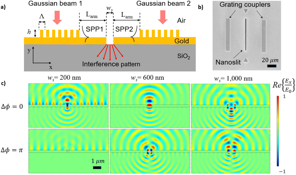 | ||
| Fig. 1 Nanoslit interferometer. (a) Schematic of the transversal section of the device showing its main components: two grating couplers deposited on top of a thick gold layer and equally distanced from a nanoslit milled into the gold layer, two grating couplers on a thick gold layer on a glass substrate equally distanced from a nanoslit milled into the thick gold layer. The grating couplers are excited by a pair of Gaussian beams, generating two SPP waves propagating in opposite directions along the air–gold interface. These plasmons interfere at the nanoslit, which is designed and optimized to support one or more resonance modes, selectively excited depending on the relative phase difference between the interfering SPP waves. (b) SEM image of a typical fabricated device. The two grating couplers and the central nanoslit are indicated with arrows for clarity. (c) Normalized electric field distributions (Re{Ex/E0}) near the nanoslit for three slit widths (ws = 200 nm, 600 nm and 1000 nm) and two phase differences between the SPP waves (Δϕ = 0 in the top row and Δϕ = π in the bottom row). For Δϕ = 0, resonant modes with an odd number of lobes along the width are excited in the nanoslit, e.g., dipole and hexapole. In contrast, for Δϕ = π, modes with an even number of lobes along the width emerge, such as the quadrupolar modes. At ws = 200 nm, no mode is observed for Δϕ = π. | ||
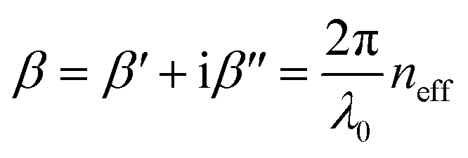
The electromagnetic modeling of the proposed interferometer was conducted using a two-dimensional (2D) finite element method (COMSOL 5.6, Electromagnetic Waves Frequency Domain module), following a similar approach to that detailed in our previous work.37,38 The calculations were specifically performed at an operating wavelength of λ0 = 850 nm. This wavelength was chosen because there are commercially available laser sources at 850 nm that offer high coherence, which is essential for interferometric applications. Additionally, light at this wavelength can be detected using Si CCD cameras, making it practical for experimental validation and measurement. The interferometer is perpendicularly excited by a pair of transverse magnetic (TM) polarized Gaussian beams of waist radius w0 = 5 μm, which illuminate the grating couplers on the device. The Gaussian beams were modeled as electromagnetic ports. The relative permittivity of the materials (gold, fused silica) were taken from established experimental tables: the relative permittivity of air, εd = 1,40 fused silica, εsub = 2.25,41 and that of gold at our operating wavelength was taken as εAu = −28.2691 + 1.7456i.42 Using these values, the effective index of refraction, neff, of the SPP waves propagating along the gold-air interface is calculated as:1
 | (1) |
and the effective wavelength λeff of the SPP waves as:
 | (2) |
The components of the interferometer were designed based on these values. For the grating coupler the pitch for maximum coupling efficiency was initially estimated as, Λ = λeff.15 Subsequently, the optimized pitch was obtained via iterative modelling until the maximum coupling efficiency was achieved (see Section 4.2). The arm length, Larm, was selected considering that the propagating SPP waves excited by the grating couplers have a finite propagation length, due to attenuation along the gold surface captured by the imaginary part of the effective index Im{neff} (see Section 4.3). Finally, the optimization of the nanoslit width, ws, was also related to λeff (see Section 4.4). Optimization of the components were performed by calculating the transmittance T of the device. To achieve this, the scattered fields emerging from the nanoslit were captured, and the Poynting vector integrated to obtain the output power of the device, which was then normalized to the incident power of the Gaussian beams.
The normalized electric field distribution (Re{Ex/E0}) near a nanoslit of varying width, ws = 200, 600 and 1000 nm, is illustrated in Fig. 1c. The top and bottom rows of the figure correspond to phase differences between the two SPP waves of Δϕ = 0 and Δϕ = π, respectively. Each column represents a different slit width: ws = 200 nm (left), ws = 600 nm (center), and ws = 1000 nm (right).
For Δϕ = 0 (top row) and for slit widths of ws = 200 and 600 nm, a dipolar mode, characterized by two distinct lobes in the electric field distribution, is observed, while for ws = 1000 nm, a hexapolar mode, exhibiting six lobes, is excited. This suggests a clear trend where modes having an odd number of lobes along the nanoslit width (e.g., dipolar, hexapolar, and potentially higher order modes) are excited. In these cases, each resonant mode exhibits a symmetric electric field distribution about the slit's vertical bisector and thus are excited by interference of the incoming SPP waves with Δϕ = 0.
In contrast, for Δϕ = π (bottom row), modes with an even number of lobes along the nanoslit width are excited. For ws = 200 nm, no mode is excited, leading to the absence of radiation through the nanoslit, whereas for ws = 600 nm, and ws = 1000 nm, a quadrupolar mode characterized by four lobes, is excited, suggesting a similar trend, with potentially higher order modes, e.g., octopolar emerging for larger slit widths. In these cases, each resonant mode exhibits an antisymmetric electric field distribution about the slit's vertical bisector and thus are excited by interference of the incoming SPP waves with Δϕ = π. This phase difference (Δϕ = π) was achieved in the simulations by adjusting the length of one of the arms (Larm), by λeff/2.
To validate the optimization of the interferometer and its components and to observe interference patterns corresponding to the multimodal excitation of the nanoslit, we fabricated structures and characterized them experimentally. To achieve precise fabrication, we employed nanofabrication techniques. The gold layer deposition was performed using physical vapor deposition (PVD) for thicker Au films and a thermal evaporator for Au gratings. Grating couplers were patterned through e-beam lithography (EBL), followed by gold deposition and lift-off processes. Nanoslits were trenched into the gold film using focused ion beam (FIB) milling. An example of a fabricated device is shown in Fig. 1b.
3 Optical test set-up
After fabrication an optical setup is used to illuminate the plasmonic interferometer with two Gaussian beams of radius w ≈ 5 μm aligned to the grating couplers. Additionally, the setup must be capable of capturing and detecting the output signal from the interferometer slit. The optical setup used is illustrated in Fig. 2a. To generate a coherent Gaussian beam of wavelength λ0 =850 nm, a single mode fiber coupled laser diode (QPhotonics, QFLD-850-100S-PM, 100 mW) was used. The fiber tip is placed in a x − y − z positioner to align the beam to the optical axis of the set-up and is positioned at the focal plane of a microscope objective used as a beam expander (Newport N-20×, NA = 0.4). The z-position of the microscope objective can be changed with a positioner to control the size of the Gaussian beam, which is perfectly collimated only when the fiber tip is exactly at the focal plane of the microscope objective. In this case, the radius of the Gaussian beam at the output of the microscope objective is w ≈ 1 mm. The beam is then TM polarized with respect to the grating couplers using a linear polarizer (Thorlabs LPVIS050-MP2) and a λ/2 waveplate (Thorlabs Achromatic 690–1200 nm). The power of the beam is controlled with a neutral density (ND) filters (Thorlabs NDUV04A) and the λ/2 waveplate controls the polarization axis of the beam allowing positioning the sample in an arbitrary angle with respect to the optical axis. The beam is then divided into two equal beams to excite both grating couplers simultaneously. This is achieved using beam splitter (BS 1) (Thorlabs 50![[thin space (1/6-em)]](https://www.rsc.org/images/entities/char_2009.gif) :50 Non-Polarizing 700–1100 nm). The pair of emerging beams travel along different optical paths, with one of them redirected to BS 2, using Mirrors 3 and 4 mounted on a positioner (Thorlabs Nanomax 300 stage) to precisely control its optical path length. The parameter ΔL represents the change in optical path length applied to one of the beams to produce a phase difference between them. For instance, to achieve a phase difference of Δϕ = π, ΔL must be equal to λ0/2. Since both mirrors are mounted on the same stage, the stage only needs to move by ΔL/2, as the configuration doubles the change in optical path length. Although this setup is reminiscent of a Mach–Zehnder interferometer, the two beams do not overlap at BS 2. Instead, they are directed to a 10× microscope objective (Nikon Plan NA = 0.25) which reduces their radius to w0 ≈ 5 μm. The size of these beams can be controlled with the beam expander, while the separation between them is adjusted by tilting mirror 3. The two Gaussian beams need to be sized to fill the aperture of the microscope objective to achieve the small beam size required in the focal plane where the gratings are located. This can be done by changing the z position of the beam expander. However, because the beam is not perfectly collimated, the two beams that travel different optical paths will have a slightly different size after focusing. This difference in size can be reduced by decreasing the optical path length of the beams.
:50 Non-Polarizing 700–1100 nm). The pair of emerging beams travel along different optical paths, with one of them redirected to BS 2, using Mirrors 3 and 4 mounted on a positioner (Thorlabs Nanomax 300 stage) to precisely control its optical path length. The parameter ΔL represents the change in optical path length applied to one of the beams to produce a phase difference between them. For instance, to achieve a phase difference of Δϕ = π, ΔL must be equal to λ0/2. Since both mirrors are mounted on the same stage, the stage only needs to move by ΔL/2, as the configuration doubles the change in optical path length. Although this setup is reminiscent of a Mach–Zehnder interferometer, the two beams do not overlap at BS 2. Instead, they are directed to a 10× microscope objective (Nikon Plan NA = 0.25) which reduces their radius to w0 ≈ 5 μm. The size of these beams can be controlled with the beam expander, while the separation between them is adjusted by tilting mirror 3. The two Gaussian beams need to be sized to fill the aperture of the microscope objective to achieve the small beam size required in the focal plane where the gratings are located. This can be done by changing the z position of the beam expander. However, because the beam is not perfectly collimated, the two beams that travel different optical paths will have a slightly different size after focusing. This difference in size can be reduced by decreasing the optical path length of the beams.
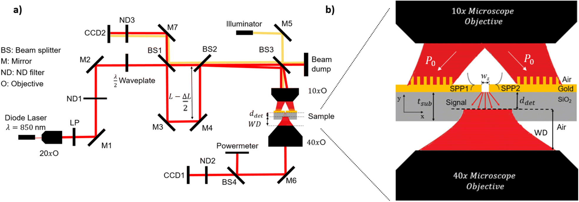 | ||
| Fig. 2 (a) Optical set-up implemented to test the nanoslit interferometer. A TM polarized Gaussian beam (λ0 = 850 nm) is expanded and divided using BS 1. The emerging beams are redirected to a 10× microscope objective, and size-reduced to match the grating couplers. The beam waist and separation can be controlled with the beam expander and mirrors 2, 3, and 4. The illuminator and BS allows collecting the reflected image by CCD camera 2. In transmission, the interferometer's radiated far-field is observed (distance of detection is 4 μm) from the nanoslit using a 40× microscope objective which images the radiated pattern on CCD Camera 1. The power associated with the transmitted light can be simultaneously measured using BS 4 and a power meter. (b) Schematic of the excitation and detection setup for the two grating couplers on the plasmonic interferometer device. Two Gaussian beams (w ≈ 5 μm) are focused onto the grating couplers using a 10× microscope objective to excite SPP1 and SPP2 traveling in opposite directions. These SPPs interfere at the nanoslit radiating a signal through the substrate and air. The transmitted signal is collected with a 40× microscope objective placed near the slit's focal point to record the interference patterns. | ||
Fig. 2b provides a close-up sketch of the device under test, illustrating excitation of the two grating couplers. This excitation generates SPP waves propagating in opposite directions, which then converge on the gold nanoslit of width ws. The modes excited in the nanoslit radiate through the substrate of thickness of tsub = 500 μm and then trough air, before reaching a 40× microscope objective (Nikon Plan, NA = 0.65). The focal plane of the microscope objective is positioned close to the gold-substrate interface (ddet ≈ 0), to avoid unwanted interference of the detected signal caused by reflections at the substrate-air interface. The magnified radiated intensity is then attenuated with a ND Filter (Thorlabs NDUV05A) and captured with CCD Camera 1 (Thorlabs DCC1645C). Before reaching the camera, the signal is redirected with mirror 6 and split by BS 4. The second beam is directed to a power meter, which is used to determineT. This is defined as the ratio between the power (P0 = 51.15 μm) of the incident Gaussian beam on the grating coupler and the power measured by the power meter (Pm), i.e.
 | (3) |
Tr accounts for the transmission losses in the receiver components (as shown in Fig. 3a), which include the 40× microscope objective, mirror 6 and BS 4. The power P0 was measured immediately after the 10× microscope objective, representing the power incident on the sample with a single Gaussian beam. To determineTr, the incident power P0 was compared with the measured power Pm without the sample in place, yielding Tr = 0.25. This indicates that only about 25% of the signal radiated from the device reaches the power meter after passing through the microscope objective, reflecting off the mirror, and being split by the 50:50 BS.
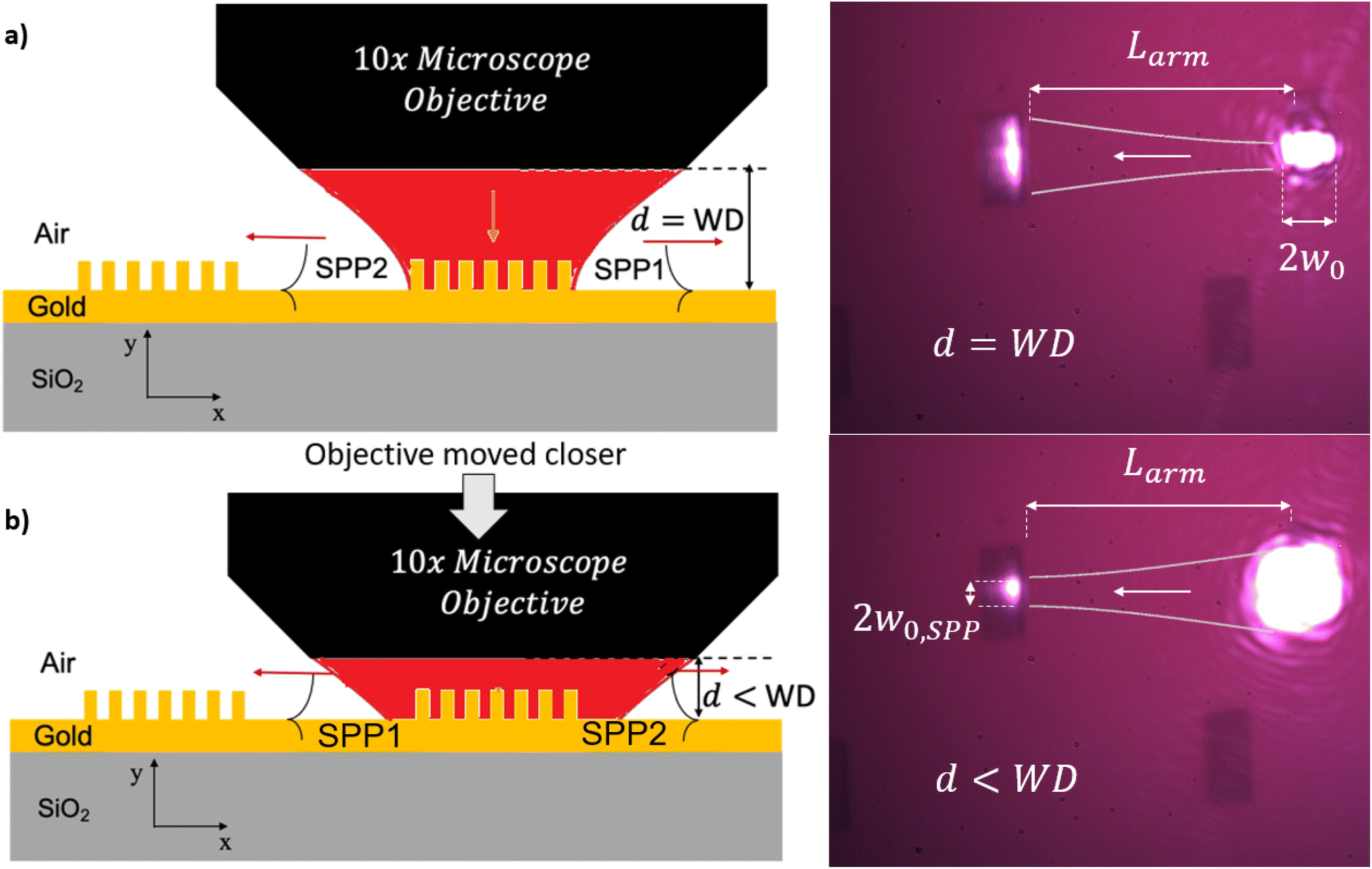 | ||
| Fig. 3 Observation of a SPP wave excited with an optimized grating coupler, traveling certain distance, and outcoupled by the second grating. (a) Left panel – microscope objective placed at a separation from the grating equal to its working distance(d = WD) such that the Gaussian beam waist w0 is located at the grating coupler. Right panel – SPP waves excited by the grating diverge in the plane of propagation, as observed from the spot uncoupled by the second grating which is wider than the incident spot (2w0,SPP > 2w0). (b) Left panel – microscope objective placed a few micrometers closer to the sample (d < WD) such that the Gaussian beam is converging at the location of the grating coupler. Right panel – the convergence of the Gaussian beam induces focusing of the SPP wave in the plane of propagation, as observed from the spot uncoupled by the second grating which is narrower than the incident spot (2w0,SPP < 2w0). | ||
The sample must also be illuminated with visible light to locate each device under test and precisely position both Gaussian beams at the center of each grating coupler. This is achieved by introducing broadband light from a fiber illuminator (Thorlabs OSL2IR) via BS 3. The unwanted beams emerging from BS 3 are captured by the beam dump. The illumination beam incident on the microscope objective is focused on and reflected by the sample. The reflected light then travels back through the microscope objective, the two BS and a ND filter (Thorlabs NDUV03A) to CCD Camera 2 (Thorlabs DCC1645C). The imaged devices, including the incident Gaussian beams, are displayed on a screen connected to the camera. Additional mirrors (mirror 1, 2, 6 and 7) are placed at different locations in the set-up to redirect the light beams as required. The 850 nm laser source can be replaced with a broadband illuminator (NKT Photonics, Super K Extreme) to find the transmission spectra of the devices, as discussed in Section 3.1. For this purpose, the power meter is replaced with an optical spectrometer (Newport OSM2-400VIS/NIR). All images obtained from CCD1 and CCD2 are presented as captured with no false colouring applied.
4 Break-out elements
Modifying the properties of the grating couplers, arm length and slit width influences T of the device and enables the tuning of the interference pattern observed on the substrate side of the nanoslit.37,38 Consequently, it is essential to experimentally investigate how variations in the parameters of these individual elements (break-out elements) affect the system. Since the interference of SPPs is not required for analysing these elements, we illuminated one grating coupler only, which excites a single SPP. This approach allows us to isolate and study the contributions of each element independently.4.1 Grating couplers – focusing of SPPs
We initially investigated the ability of a grating coupler to excite focused SPPs by exciting a grating coupler with a converging Gaussian beam of wavelength λ0 = 850 nm and radius w ≈ 5 μm. For these experiments, a pair of grating couplers with optimized parameters (height h = 54 nm, pitch Λ = 786 nm, duty cycle dc = 0.68 and 12 periods), were defined and separated by a distance of Larm = 40 μm, as sketched in Fig. 1a. One of the gratings was used to in-couple SPP waves at the air–gold interface, and the second one to out-couple them. By changing the distance d of the sample from the 10× microscope objective (cf. Fig. 2a), the size of the Gaussian beam exciting the grating coupler can be modified; this is illustrated in Fig. 3. When the objective is placed at its working distance from the sample (d = WD), the Gaussian beam illuminates the grating having its waist at the grating plane (2w0 in diameter). In this case, the SPP wave diverges along the air–gold interface in the plane of propagation, and once it reaches the second grating, it is out-coupled with a larger width than the incident beam (2w0,SPP > 2w0), as shown in Fig. 3a. Alternatively, if the sample is placed closer to the objective (d < WD), as shown in Fig. 3b, the Gaussian beam impinges onto the grating while it is still converging, resulting in a SPP wave that focuses as it propagates along the air–gold interface. In this case, the second grating out-couples the SPP wave with a smaller width than the exciting beam (2w0,SPP < 2w0). In this manner the SPP beam waist w0,SPP (SPP focus) can be placed on the out-coupling grating, as shown in Fig. 3b, or on any other feature on the chip. This method of tuning the SPP beam diameter is useful for controlling the size of the plasmonic waves that excite the resonant modes of the nanoslit and improves the visibility on the detection camera in the interferometric experiments discussed in Section 5. These experiments provide a qualitative demonstration of the (out-) coupling and existence of SPP waves by observing the reflection in CCD Camera 2 (cf. Fig. 2a). Henceforth, experiments are conducted to observe and measure the fields radiated from the nanoslit on the substrate side of the device with the transmission recorded by CCD Camera 1 and the optical power meter or spectrometer (cf. Fig. 2a).4.2 Grating couplers – spectral response, pitch and number of periods
The design process to optimize the grating couplers is similar to that applied in previous work.37,38 The parameters to optimize are the ridge height h, pitch Λ, duty cycle dc, and number of ridges (Fig. 1a). The height of the ridges is defined by thermal evaporation after e-beam lithography exposure. The ridge height achieved for all devices is h = 54 nm which is close to the value of h = 60 nm ideally needed for maximum coupling efficiency. During the designing process, the duty cycle was fixed to dc = 0.5, and the duty cycle achieved in all devices after fabrication is dc = 0.68, as can be observed in Fig. 4a, where a grating coupler of pitch Λ = 796 nm is shown – the ridges are slightly wider than the trenches.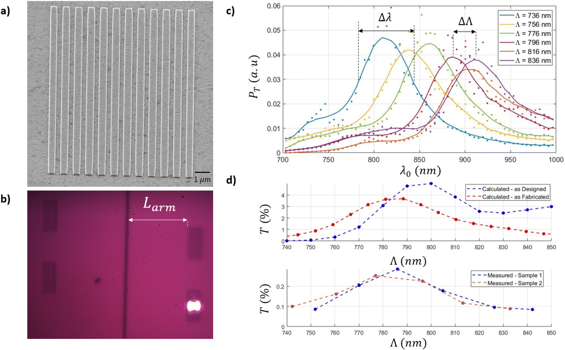 | ||
| Fig. 4 Grating spectral response and pitch variation. (a) SEM image of a grating coupler (Λ = 796 nm and dc = 0.68). (b) Reflected image showing a device under test, captured in situ using CCD Camera 2. This set of grating couplers is arranged along the length of the nanoslit of width ws = 610 nm. The grating pitches vary from Λ = 736 nm to Λ = 836 nm, and the duty cycle is set to dc = 0.68. The bottom right grating is excited with a Gaussian beam of radius w ≈ 5 μm centered on the grating. (c) Wavelength response of the transmitted power PT of the gratings and nanoslit combination, excited with broadband light and measured using a spectrometer. Note that PT is presented in arbitrary units, as it was not possible to accurately determine the power of the input beam during the measurements. When the pitch of the grating increases, the wavelength of maximum transmittance increases proportionally. (d) T, of gratings excited with a laser centered at λ0 = 850 nm, for gratings of various pitch, Λ. The top panel shows the calculated results of the designed (blue curve) and as-fabricated (red curve) gratings. The bottom panel shows the experimental results for two samples each bearing several gratings, demonstrating a similar trend with pitch compared to the calculations. | ||
This section explores the effects on the transmitted light on devices composed of one grating separated from a nanoslit by Larm = 40 μm, when the grating pitch Λ and number of ridges are varied. The gratings were designed for a normally-incident TM polarized Gaussian beam of wavelength λ0 = 850 nm and beam waist radius of w0 = 5 μm. The maximum coupling efficiency of the designed grating occurs for a pitch of Λ = 800 nm, composed of 12 periods. Under these conditions, the size of the grating coupler is very close to the diameter of the incident Gaussian beam. The designs were comprised of a range of pitches from Λ = 736 nm to Λ = 836 nm in steps of ΔΛ = 10 nm. Fig. 4b shows the device used for the pitch experiments. It comprises of a linear arrangement of grating couplers on a gold film of thickness tAu = 311 nm, positioned a distance of Larm = 40 μm from a nanoslit of width ws = 610 nm milled into the gold film.
The grating couplers were initially excited with a Gaussian beam, as previously described, generated from a broadband source. To obtain the spectrum of the transmitted power PT for each grating coupler and nanoslit combination, the output signal radiated by the nanoslit was measured using a spectrometer. This is illustrated in Fig. 4c. Although the grating pitch varies in increments of ΔΛ = 10 nm, we present the results every ΔΛ = 20 nm to maintain clarity and prevent graph saturation. Due to the high power of the incident broadband source, the spectrometer became saturated, requiring the use of ND filters to accurately capture the source spectrum. PT was calculated by comparing the source spectrum with the measured spectrum radiated by the nanoslit for different grating pitches, which did not require attenuation. Since the accurate power measurements for the incident broadband source were not obtained, PT is presented in arbitrary units. Despite this, as shown in Fig. 4c, the spectra exhibit a full width at half maximum (FWHM) of approximately, Δλ ≈ 100 nm for all grating pitches, and the peak transmittance shifts linearly with increasing grating pitch, as expected.
Replacing the broadband illuminator with at laser source at λ0 = 850 nm, the incident power of the Gaussian beam (P0 = 224 μW) can be compared to the transmitted power to obtain T for each pitch Λ, The top panel of Fig. 4d shows the calculated T for the designed and fabricated cases, calculated using:
 | (4) |
The bottom panel of Fig. 4d shows the experimental T obtained using eqn (3) for two samples bearing devices. The maximum T of the tested devices occurs for Λ = 786 nm, which is very close to theoretical expectations (1.75%). However, the experimental T is ∼10% of the calculated values because of non-idealities in the experimental case, which include: (i) roughness of the gold layer (Rq = 5.24 nm) and grating ridges (Rq = 5.58 nm) characterized by the root mean square value Rq of the height variations on the surfaces, (ii) reflections occurring at the glass-air interface along the bottom of the substrate (unaccounted for theoretically), which cause additional losses; (iii) deviations in the grating coupler thickness due to fabrication limitations, which reduce coupling efficiency; (iv) variations in the pitch and duty cycle of the gratings caused by defocusing effects during E-beam lithography, leading to non-ideal grating structures; and (v) 2D calculations using a 1D Gaussian beam, which approximates the 3D nature of the system and overestimates slightly the power coupled by the gratings. These factors collectively explain the differences in transmittance observed across all measurements, such that the experimental T is ∼10% of the calculated values for all tested structures. Despite the reduced experimental T relative to design, the output from the device is readily detected using a standard CCD camera, power meter, and spectrometer.
Aligning the center of the Gaussian beam to the center of the grating coupler is essential if meaningful comparisons are to be made with the computations. With centered alignment, the power of the excited SPP waves is equal in both directions of propagation (left and right), whereas if the beam is aligned off-center close to the edge of a grating coupler, one SPP wave is preferentially excited along one direction. For this set of grating coupler experiments, it is particularly important to achieve centered alignment because it was observed that the wavelength of maximum transmission of the grating varies with the position of the Gaussian beam relative to the grating. Centered alignment was achieved by visualizing the reflected beam with CCD Camera 1 and optimizing the alignment. Fig. 4b illustrates a case where the Gaussian beam is placed at the center of the grating coupler, whereas Fig. 5b shows a case where the beam is aligned near the left edge of the grating.
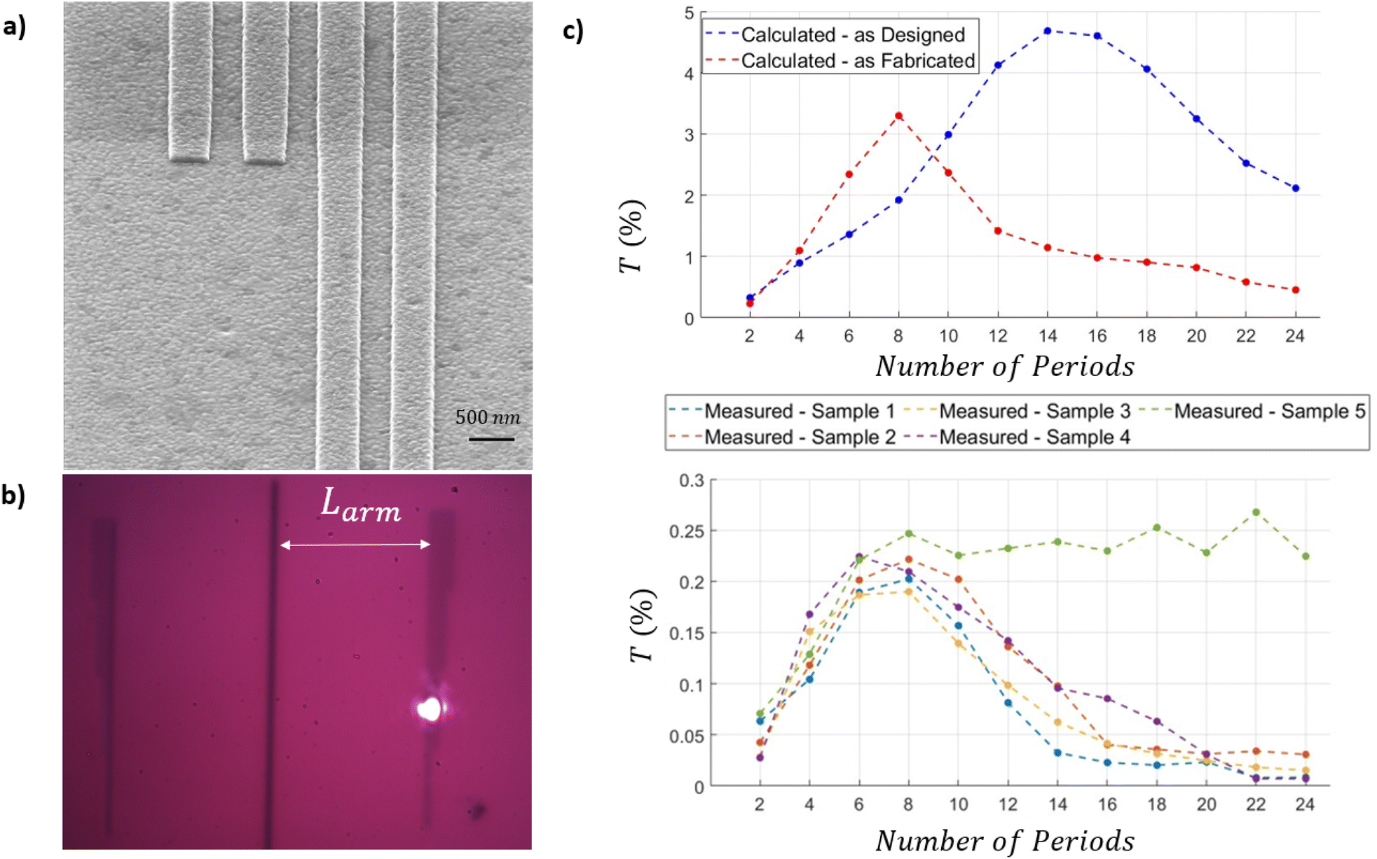 | ||
| Fig. 5 The effect of variation in grating period. (a) SEM image of a section of the sample showing an increase in the number of periods from 2 to 4. (b) Reflected image showing a device under test. This set of grating couplers is arranged along the length of a nanoslit of width ws = 610 nm. The grating periods vary from 2 to 24. A grating coupler is excited with a Gaussian beam of radius w0 ≈ 5 μm, aligned at the edge of the grating. (c) The top panel shows the calculated T as a function of the number of grating periods, for designed (blue curve) and fabricated (red curve) gratings, yielding an optimal number of periods of 14 and 8 respectively. The bottom panel presents measured results obtained on 5 samples, demonstrating very similar trends to the calculated case. Sample 5 was tested by aligning the center of the Gaussian beam along the edge of a grating, rather than along its center, thereby maximizing the coupling efficiency of SPPs propagating in the direction of the nanoslit. With this alignment along the edge, T remains constant as the number of periods increases beyond 8. | ||
In addition to the grating pitch Λ variation, another important design parameter of the grating couplers is the number of periods ng. Fig. 5a shows a SEM image of a section of the experiment where the number of ridges in a grating increase from 2 to 4. Five identical samples were fabricated, each of them consisting of a series of 3 gratings that increase in number of ridges in steps of two. In Fig. 5b, a section of a sample is shown where a Gaussian beam of waist radius w0 ≈ 5 μm excites the left edge of a grating coupler. With this alignment, the SPP wave is preferentially excited to the left (towards the nanoslit). All the samples were tested with the beam centered on the grating except for one case – Sample 5. Fig. 5c shows T as the number of ridges increases. The top panel shows calculations for the designed (blue curve) and fabricated (red curve) cases. In the designed case, the number of periods that maximizes the T is ng = 14. However, for the fabricated case, the maximum T decreases by ≈42.86% and the optimal number of periods is ng = 8. This finding is experimentally corroborated, as can be observed in the bottom panel of Fig. 5c. Samples 1 to 4 exhibit the same behavior, confirming the calculated prediction. Sample 5 was excited with the Gaussian beam aligned to the left edge of the grating couplers (nearest the nanoslit). In this case, the maximum T remains constant after the optimal number of ridges is reached.
To achieve maximum coupling of SPPs propagating along one direction from a grating under normal incidence, it is necessary to illuminate the edge. With this approach, the grating coupler will always perform optimally once the optimal number of periods is reached. Conversely, if it is necessary to excite SPPs in both directions of propagation, the best strategy is to illuminate the grating with a beam centered on the grating. In this scenario, it is crucial to use the optimal number of periods such that the grating coupler matches the size of the incident Gaussian beam. This minimizes the outcoupling effect that a large grating induces and maximizes the efficiency of the grating coupler.
4.3 Cut back measurements
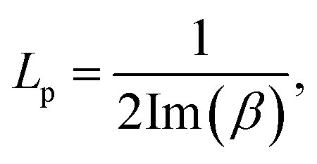
The length of the interferometer arm (Larm) is the distance that the SPP waves must travel to reach the nanoslit. This distance must not significantly exceed the SPP propagation length Lp. Considering a power decay of 1/e from the excitation location of the SPP wave at the edge of the grating, Lp can be calculated as:1
 | (5) |
 | (6) |
In our experiments the arm length was varied from Larm = 20 to 130 μm. Fig. 6a shows a SEM image of a portion of a sample under test, which comprises of a linear arrangement of grating couplers along the vertical direction, each grating having a different distance from the nanoslit. In this experiment, a Gaussian beam of radius of w0 ≈ 5 μm excites a SPP wave via an optimized grating coupler (h = 54 μm, Λ = 786 nm, dc = 0.68, and ng = 12 periods), as shown in Fig. 6b. After propagating over Larm, the SPP wave excites the gold nanoslit of width ws = 610 nm, exciting resonant modes therein, resulting in radiated fields detected on the substrate side. Calculated T (using eqn (4)), for different arm lengths is shown in the top panel of Fig. 6c. The power carried by the SPP wave decays exponentially when the arm length is increased. At a fixed wavelength of operation, λ0 = 850 nm, the attenuation constant β′′ depends only on the relative permittivity of the materials used and is estimated to be 9.00 mm−1 from an exponential fit. This value is 6% larger than that calculated using eqn (1)–(6). Measured T of devices of different arm length Larm on three samples is shown in the bottom panel of Fig. 6c. They exhibit the same exponential trend consistent with the computations. The average attenuation coefficient obtained experimentally is 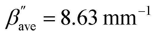 and this value is 1.64% smaller than the value estimated using eqn (1)–(6). The experimental attenuation coefficient (Fig. 6c, bottom panel) is closer to the analytical result than the one determined by simulating the entire system (Fig. 6c, top panel) possibly due to limitations in discretizing the system.
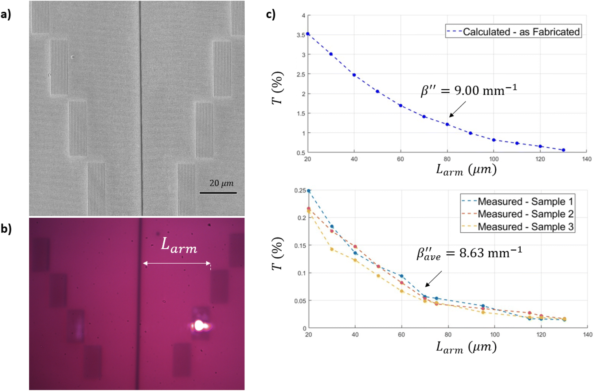 | ||
Fig. 6 Cut-back measurements. The distance between the grating and the nanoslit of width ws = 610 nm (arm length) varies from Larm = 20 to 130 μm. (a) SEM image of one of the samples comprised of a linear arrangement of grating couplers along the vertical direction, each grating having a different distance from the nanoslit. (b) Reflected image showing a device under test. A grating coupler is excited with a Gaussian beam of radius w0 ≈ 5 μm, aligned near the left edge of the grating. (c), T, for different arm lengths, Larm. The top panel shows the calculated T as function of Larm for the simulated case. The attenuation constant can be obtained from an exponential fit of the transmittance curve and is β′′ = 9.00 mm−1, which varies by 6% from the analytical calculation. The bottom panel shows a set of experiments on three samples demonstrating a very similar trend to the calculated cases. The average decay constant obtained experimentally is  , which differs by 1.64% from the analytical calculation. , which differs by 1.64% from the analytical calculation. | ||
4.4 Nanoslit width
Previous studies have shown that the resonance modes in a nanoslit are highly sensitive to variations in the slit width ws.37,38 The slit width affects both T and the radiation pattern and consequently has implications on the performance of the device. Nanoslits of different widths were fabricated in a gold film deposited on a fused silica substrate via FIB milling. Fig. 7a shows a SEM image of three nanoslits of different widths (ws = 205, 505 and 805 nm). The fabricated test samples feature a 3-segment nanoslit that exhibits a variable width along its length. Each of the 3 segments is 80 μm long. The nanoslit width varies linearly from at ws = 205 nm to ws = 505 nm in segment 1, from ws = 505 nm to ws = 805 nm in segment 2, and from ws = 805 nm to ws = 1075 nm in segment 3. This segmentation was necessary due to the limitations of the focused ion beam (FIB) milling process. Optimized grating couplers were fabricated alongside the nanoslit (h = 54 nm, Λ = 786 nm, dc = 0.68, and ng = 12 periods), at a distance of Larm = 40 μm from the nanoslit, and excited with a TM polarized Gaussian beam of wavelength λ0 = 850 nm and radius w0 ≈ 5 μm to excite a single SPP wave, that then propagates to the nanoslit exciting resonant modes therein. Depending on the width of the slit, the modes exhibit different spatial field distributions, which are described below, producing characteristic radiation patterns. Fig. 7b shows an image captured with CCD Camera 2, showing the implementation of this experiment. The Gaussian beam was positioned vertically along a grating to access a nanoslit region of different width. | ||
| Fig. 7 The effect of varying the width of the nanoslit. (a) SEM image of nanoslits of different widths ws = 205, 505 and 805 nm milled via FIB in a gold layer of thickness tAu = 311 nm on a fused silica substrate. (b) Reflected image showing a device under test. The nanoslit is excited by a single SPP wave launched from a grating. The width of the nanoslit achieved after fabrication decreases linearly along the length of the slit from ws = 1075 to 205 nm (top to bottom), and the grating couplers are uniform over the entire length of the slit. The left grating coupler is excited with a Gaussian beam of radius w0 ≈ 5 μm, aligned near the left edge of the grating. (c) T for different slit widths ws is computed (top panel) and measured on two samples (bottom panel). | ||
Top panel of Fig. 7c shows the calculated T (using eqn (4)), as a function of the slit width ws for the calculated device. Interestingly, note that T peaks when the slit width increases from ws ≈ 200 nm to ws ≈ 500 nm. Recall that only the dipolar resonance is supported by the nanoslit over this range of widths (Fig. 1c, left panel). Beyond ws ≈ 500 nm, the quadrupolar mode (Fig. 1c, center panel) is also supported, and the transmission decreases, reaching a minimum when the slit width is approximately ws ≈ 750 nm. This behavior is somewhat counterintuitive because normally, as an optical aperture increases in size, the transmitted power increases as well – but this occurs for direct illumination of an aperture, which is not the case here. Rather the aperture (nanoslit) in our case is excited by a propagating SPP which excites resonant modes therein with different weights depending on field overlaps. Thus, beyond ws ≈ 500 nm a linear combination of resonant modes is excited which interfere in the nanoslit, altering the radiation pattern and power radiated therefrom. If the slit width is increased beyond ws ≈ 750 nm, the T increases again, and a hexapolar mode is excited (Fig. 1c, right panel). This phenomenon is corroborated experimentally, as shown in the bottom panel of Fig. 7c. The experimental results demonstrate that T decreases similarly, mirroring the behavior observed in the calculated case. This consistency between experimental and theoretical results provides robust evidence of the first experimental demonstration of multimode excitation in a nanoslit.
We investigate the multimode operation of the nanoslits in the gold film by imaging the intensity radiated by the nanoslits through the substrate with the receiver microscope objective and CCD Camera 1 (cf. Fig. 2a). The focal plane of this objective was positioned very close to the gold-substrate interface to magnify the nanoslit. The imaging process is visual, allowing for a few micrometers of tolerance in the receiver position where the slit appears well-defined. Once the nanoslit is imaged in the substrate side, the grating coupler on the top side is excited by the Gaussian beam to launch an SPP toward the nanoslit (cf. Fig. 7b). Images of the radiation emitted by nanoslits of various widths ws, under SPP excitation, are shown in Fig. 8a, revealing different spatial distributions for different nanoslit widths ws. The orange/red colour band in the images are due to the nanoslit illuminated by a broadband illuminator to make it clearly visible, whereas the bright localised spots correspond to the out-coupled surface plasmon waves generated by the monochromatic laser (850 nm). For a slit width of ws ≈ 250 nm, a symmetrical radiation pattern exhibiting a single lobe is observed, suggesting that only the dipolar resonant mode of the nanoslit is supported (cf. Fig. 1c, left panel). As the slit width increases to ws ≈ 450 nm, the radiation pattern loses its symmetry, and the intensity maximum shifts away from the center of the nanoslit. For a slit width of ws ≈ 550 nm a second lobe becomes observable and persists up to ws ≈ 750 and 850 nm, consistent with the emergence of the quadrupolar mode in the nanoslit. One lobe is less intense than the other because the nanoslit is excited by a single SPP wave (launched from the right grating and propagating towards the left – cf. Fig. 7b). Perfect symmetry in the two radiated lobes is only achieved when the nanoslit is excited by two identical counterpropagating SPP waves that are out of phase, thereby exciting the quadrupolar mode only (cf. Fig. 1c, right panel), as demonstrated in the interference experiments discussed in the next section. For a slit width of ws ≈ 950 nm the radiation pattern becomes more complex, suggesting the emergence of a third resonant mode. For the slit width ws ≈ 950 nm, the radiated signal suggests a three-lobe distribution which we associate with the hexapole predicted in Section 2. Fig. 8b plots the calculated distribution of the magnitude of the Poynting vector, at a distance of ddet = 4 μm below the gold-substrate interface. The Poynting vector was calculated by exciting a single grating coupler in the simulation with a Gaussian beam of power P0 = 1 W m−1 (2D simulation), which was coupled to SPP waves and radiated by the nanoslit. The transition in the number of lobes observed experimentally matches qualitatively the calculations, corroborating our observation of multimode excitation of nanoslits.
 | ||
| Fig. 8 Experimental and theoretical demonstration of multimode excitation in nanoslits in a gold film, for widths ranging from ws ∼ 250 to 950 nm. (a) Experimental visualization of the intensity distribution radiated by nanoslits in the gold film of different widths ws. The intensity is imaged with a 40× (NA = 0.6) objective whose focal plane is positioned very close to the gold-substrate interface. (b) Calculated distribution of the magnitude of the Poynting vector, 4 μm below nanoslits of different width ws. As the nanoslit width increases, an increasing number of resonant modes become supported therein. For ws ∼ 250 and 450 nm, the nanoslit supports only the dipolar mode, resulting in a single-lobed radiation pattern. For ws ≈ 550, 750 and 850 nm, the dipolar and quadrupolar modes are supported, resulting in a two-lobed radiation pattern. For ws ≈ 950 nm, a third lobe appears in the radiated signal, suggesting that a hexapolar mode is supported by nanoslits of this width. The experimental images in (a) match qualitatively with the calculated distributions in (b). | ||
5 Interference of SPP waves on multimode nanoslits
Finally, we investigate the interference of SPP waves on nanoslits and the selective excitation of resonances therein. The number of resonant modes is determined by the nanoslit width ws, and their selective excitation by the phase difference Δϕ between the two SPP waves exciting the nanoslit. For interference of two SPP waves, grating couplers on either side of a nanoslit are excited by a pair of coherent Gaussian beams, with their relative phase adjusted by varying the optical path length, as described in Section 2. Fig. 9a shows an image, where a device under test is illuminated by two beams of radii w0 ≈ 5 μm. Both Gaussian beams must have the same size and power to interfere strongly at the nanoslit. However, there is always a small difference in the size of the Gaussian beams because they are focused by the 10× objective illuminated by non-collimated Gaussian beams which travel two different optical paths and are slightly off the optical axis. To match the size of both SPP waves as closely as possible at the nanoslit it is necessary to adjust the z position of the beam expander, shown in Fig. 2a. At the same time, matching the power of the two SPP waves is straightforward: by misaligning one of the beams at its corresponding grating coupler and reducing its power until it matches that of the second beam. | ||
| Fig. 9 Experimental and theoretical demonstration of selective modal excitation in a multimode nanoslit by the interference of SPP waves. (a) Simultaneous excitation of a pair of grating couplers by Gaussian beams, producing a pair of SPP waves traveling in opposite directions and interfering on the gold nanoslit. (b) The intensity distribution radiated by a nanoslit of width ws ∼ 600 nm through the substrate, imaged at a distance of ddet ≈ 4 μm. For ws ≈ 600 nm, the dipolar and quadrupolar modes of the nanoslit are selectively excited when the phase difference between the interfering SPP waves is Δϕ = 0 (top panel) and Δϕ = π (bottom panel). (c) Calculated distribution of the magnitude of the Poynting vector, 4 μm below nanoslits of different width, ws = 200, 600, and 1000 nm. The nanoslits are excited by a pair of SPP waves of phase difference Δϕ = 0 and π. The nanoslit can support the dipolar, quadrupolar and hexapolar modes depending on the phase difference Δϕ between the interfering SPP waves and the nanoslit width ws. (d) Horizontal cut of the measured intensity distribution radiated below nanoslits of different width, captured by a 40× (NA = 0.6) objective and a CCD camera. (e) T obtained by integrating the calculated (blue curve) and measured (red dots) intensity radiated by the nanoslits as a function of the phase difference between the interfering SPP waves over the range Δϕ = 0 to 2π, yielding the periodic transfer characteristic of the interferometer. | ||
The phase of one of the SPP waves is shifted by adjusting the position of mirrors 3 and 4 in the optical setup shown in Fig. 2a, with a mechanical stage controlled by a piezoelectric actuator. This stage moves in steps of ≈6 nm, and needs to be shifted ΔL = λ0/8 ≈ 107 nm to change the relative phase between both SPP waves by Δϕ = π. Fig. 9b shows the intensity radiated from a nanoslit of width ws ≈ 600 nm, through the substrate, associated with the dipolar (top panel) and quadrupolar (bottom panel) resonant modes, when the relative phase difference Δϕ between the SPP waves is Δϕ = 0 and Δϕ = π. The dipolar mode is characterized by a single radiated lobe, whereas the quadrupolar mode exhibits a pair of radiated lobes. Due to the imperfect collimation of the initial beam, the two SPP waves do not overlap precisely, resulting in an interference pattern with unequal sized lobes.
The calculated intensity distributions, defined by the real part of the normalized Poynting vectors Re{S}, are plotted in Fig. 9c for different nanoslit widths, ws ≈ 200, 600 and 1000 nm. For ws ≈ 200 nm, only the dipolar resonant mode is supported by the nanoslit and the radiated intensity exhibits a centered lobe whose amplitude varies with Δϕ to become null for Δϕ = π, as observed from Fig. 9c (left panel). This is corroborated experimentally in Fig. 9d (left panel), although noise, likely due background light, decreases the signal visibility. For ws ≈ 600 nm, the dipolar mode is excited for Δϕ = 0 and the quadrupolar mode is excited for Δϕ = π, and the intensity distribution transitions from a single lobe to a pair of equally sized lobes, as observed from Fig. 9c (center panel). This is also confirmed experimentally in the corresponding plot of Fig. 9d (center panel). For ws ≈ 1000 nm, simulations indicate the generation of a third lobe in the radiated field intensity distribution, due the excitation of a hexapolar mode for Δϕ = 0, as shown in Fig. 9c (right panel). The corresponding experimental result in this case does not agree very well with the computations because the numerical aperture of the objective limits resolution of three lobes. It is important to note that the experimental curves in Fig. 9d are normalized to their maximum value, as these intensity distributions are computed by analyzing a 2D line of the observed modes, where the intensity is related to the intensity of each pixel. This makes it difficult to determine the real values of the Poynting vector and the actual size of the lobes, which is why the curves are normalized and shown in arbitrary units. However, because the patterns were measured as close as possible to the slit, we expect the lobe sizes to be comparable to those calculated in Fig. 9c.
Integrating the intensity distribution yields the transmittance of the interferometer. These values were calculated as a function of Δϕ and are plotted in Fig. 9e, showing the transfer characteristics of the system for each case of nanoslit width ws. The calculated results (blue curves) agree very well with the experimental values (red dots). In this case, integrating the intensity provides the power at the output, as was done in all the previous experiments. However, for the current scenario, the input power exciting the interferometer, P0, consists of two Gaussian beams with P0 = 1 W m−1. T is therefore calculated by integrating the intensity distributions of Fig. 9c and comparing it with this total input power. Specifically, T is calculated with E. (4), however, this time P0 = 2 W m−1, because it accounts for the power two Gaussian beams. This is done for phase differences from Δϕ = 0 to Δϕ = 2π. These phase differences correspond to changes in the arm length of the interferometer, from ΔL = 0 to ΔL = λeff/2. This is presented in Fig. 9e as the blue curve, with the transmittance scale on the left side of the figure.
On the experimental side, the measurements were performed using the same method explained earlier, where the 2D intensity distributions were captured along a cutline. After integrating for each Δϕ (red points), the values of T were normalized to their maximum value and are shown on the right y-axis of Fig. 9e. This was done for all three slit widths. In the experiments visibility is significantly reduced, likely due to dark noise and low coherence of the light source. However, when the theoretical curve is plotted alongside the experimental data, we observe a strong overlap, confirming the periodic behavior of the interferometer as a function of the relative phase difference between the SPP waves Δϕ.
6 Conclusions
In this study, we present a comprehensive theoretical and experimental analysis of the controlled interference of two counterpropagating SPP waves in a multimode gold nanoslit structure. The SPP waves were generated by exciting grating couplers positioned symmetrically on either side of the nanoslit, each using a Gaussian beam. We demonstrate the ability to precisely modulate the interference pattern by altering the geometrical parameters of the gold nanoslit, enabling the selective excitation of one, two or more resonance modes at the slit. Our theoretical predictions on how the transmitted pattern depends on various geometrical factors—such as grating coupler pitch, height, duty cycle, and nanoslit dimensions—were in good agreement with experimental results. This novel approach for manipulating multimodal resonances in nanoslits offers significant potential for precision applications. The capability to tailor mode excitation opens new possibilities in optical sensing and biosensing, where heightened sensitivity and multiplex detection are essential. Furthermore, the interferometer design developed here could be integrated into photonic circuits, providing scalable solutions for miniaturized optical devices. These advancements hold great promise for applications such as environmental monitoring, medical diagnostics, and next-generation wearable technologies, including smart watches and mobile devices.Data availability
Data for this article, including codes, simulated data and experimental data are available at: https://www.scidb.cn/en/s/UjUzue.Conflicts of interest
There are no conflicts to declare.Acknowledgements
Funding provided by the Natural Sciences and Engineering Research Council of Canada, grant number 210396, CONAHCYT National System of Researchers (SNI 1047863), Federico Baur Endowed Chair in Nanotechnology (ILST002-23ID69001), Graduate Seed Program of Tecnológico de Monterrey, CONAHCYT (CVU 900707) are gratefully acknowledged.References
- S. A. Maier, Plasmonics: Fundamentals and Applications, Springer, New York, 2007, vol. 1 Search PubMed.
- J. Zhang, L. Zhang and W. Xu, J. Phys. D: Appl. Phys., 2012, 45, 113001 CrossRef.
- J. M. Pitarke, et al., Rep. Prog. Phys., 2006, 70, 1 CrossRef.
- A. V. Zayats, I. I. Smolyaninov and A. A. Maradudin, Phys. Rep., 2005, 408, 131–314 CrossRef CAS.
- L. Novotny and B. Hecht, Principles of Nano-Optics, Cambridge University Press, Cambridge, 2012 Search PubMed.
- W. L. Barnes, A. Dereux and T. W. Ebbesen, Nature, 2003, 424, 824–830 CrossRef CAS PubMed.
- E. N. Economou, Phys. Rev., 1969, 182, 539 CrossRef.
- R. Zia and M. L. Brongersma, Nat. Nanotechnol., 2007, 2, 426–429 CrossRef CAS PubMed.
- O. Graydon, Nat. Photonics, 2012, 6, 139 CrossRef.
- Y. Gao, et al., ACS Nano, 2011, 5, 9836–9844 CrossRef CAS PubMed.
- M. Thomaschewski, et al., Nano Lett., 2022, 22, 6471–6475 CrossRef CAS PubMed.
- C. Haffner, et al., Nat. Photonics, 2015, 9, 525–528 CrossRef CAS.
- F. Lotfi, N. Sang-Nourpour and R. Kheradmand, Opt Laser. Technol., 2021, 137, 106809 CrossRef CAS.
- R. S. El Shamy, D. Khalil and M. A. Swillam, Sci. Rep., 2020, 10, 1293 CrossRef CAS PubMed.
- A. Khan, et al., Appl. Phys. Lett., 2013, 103, 111 CrossRef.
- H. Fan, R. Charbonneau and P. Berini, Opt. Express, 2014, 22, 4006–4020 CrossRef CAS PubMed.
- R. Charbonneau, et al., Sens. Actuators, B, 2008, 134, 455–461 CrossRef CAS.
- M. Pu, et al., Opt. Express, 2010, 18, 21030–21037 CrossRef CAS PubMed.
- A. Sánchez-Ramírez, et al., Opt Laser. Technol., 2024, 168, 109813 CrossRef.
- Y. Gao, et al., Opt. Express, 2013, 21, 5859–5871 CrossRef CAS PubMed.
- S. B. Nimse, et al., Analyst, 2016, 141, 740–755 RSC.
- A. L. Washburn, et al., Anal. Chem., 2010, 82, 69–72 CrossRef CAS PubMed.
- B. Bottazzi, et al., J. Biomed. Opt., 2014, 19, 017006 CrossRef PubMed.
- G. Breglio, et al., Sens. Actuators, B, 2004, 100, 147–150 CrossRef CAS.
- H. Raether, Surface Plasmons on Smooth Surfaces, Surface Plasmons on Smooth and Rough Surfaces and on Gratings, 2006, pp. 4–39 Search PubMed.
- A. P. Hibbins, B. R. Evans and J. R. Sambles, Science, 2005, 308, 670–672 CrossRef CAS PubMed.
- C.-Z. Deng, et al., ACS Photonics, 2020, 7, 2915–2922 CrossRef CAS.
- F. Ding, R. Deshpande and S. I. Bozhevolnyi, 2018 Progress in Electromagnetics Research Symposium (PIERS-Toyama), IEEE, 2018 Search PubMed.
- H. Mühlenbernd, et al., ACS Photonics, 2016, 3, 124–129 CrossRef.
- M. Kraft, et al., Phys. Rev. X, 2015, 5, 031029 Search PubMed.
- M. Lequeux, et al., Plasmonics, 2020, 15, 1653–1660 CrossRef CAS.
- M. Khodami and P. Berini, J. Opt. Soc. Am. B, 2019, 36, 1921–1930 CrossRef CAS.
- C. Genet and T. W. Ebbesen, Nature, 2007, 445, 39–46 CrossRef CAS PubMed.
- Z. Zhang, et al., Opt. Express, 2015, 23, 10732–10740 CrossRef CAS PubMed.
- Y. Gao, et al., Lab Chip, 2013, 13, 4755–4764 RSC.
- Q. Wang, J. Bu and X.-C. Yuan, Opt. Express, 2010, 18, 2662–2667 CrossRef CAS PubMed.
- U. Felix-Rendon, P. Berini and I. De Leon, Opt. Express, 2021, 29, 17365–17374 CrossRef CAS PubMed.
- M. Valero, I. De Leon, M. Ray and P. Berini, Appl. Opt., 2025, 64, 50–63 CrossRef.
- J. J. Burke, G. I. Stegeman and T. Tamir, Phys. Rev. B:Condens. Matter Mater. Phys., 1986, 33, 5186 CrossRef CAS PubMed.
- M. Born and E. Wolf, Principles of Optics: Electromagnetic Theory of Propagation, Interference and Diffraction of Light, Elsevier, 2013 Search PubMed.
- I. H. Malitson, J. Opt. Soc. Am. A, 1965, 55, 1205–1209 CrossRef CAS.
- P. P. Johnson and R. W. Christy, Phys. Rev. B:Condens. Matter Mater. Phys., 1974, 9, 5056 CrossRef CAS.
| This journal is © The Royal Society of Chemistry 2025 |