
 Open Access Article
 This Open Access Article is licensed under a
 Creative Commons Attribution 3.0 Unported Licence
A customizable wireless potentiostat for assessing Ni(OH)2 decorated vertically aligned MoS2 thin films for electrochemical sensing of dopamine†
Topias Järvinen *a,
Olli Pitkänena,
Tomi Laurilab,
Minna Mannerkorpic,
Simo Saarakkalac and
Krisztian Kordasa
*a,
Olli Pitkänena,
Tomi Laurilab,
Minna Mannerkorpic,
Simo Saarakkalac and
Krisztian Kordasa
aMicroelectronics Research Unit, Faculty of Information Technology and Electrical Engineering, University of Oulu, PO Box 4500, 90014, Finland. E-mail: topias.jarvinen@oulu.fi
bDepartment of Electrical Engineering and Automation, School of Electrical Engineering, Aalto University, PO Box 13500, 00076 Aalto, Finland
cResearch Unit of Health Sciences and Technology, Faculty of Medicine, University of Oulu, PO Box 5000, 90014, Finland
First published on 8th January 2025
Abstract
In this study, we show that on-chip grown, vertically aligned MoS2 films that are decorated with Ni(OH)2 catalyst are suitable materials to be applied as working electrodes in electrochemical sensing. The constructed sensors display a highly repeatable response to dopamine, used as a model analyte, in a large dynamic range from 1 μM to 1 mM with a theoretical detection limit of 0.1 μM. In addition, to facilitate practical implementation of the sensor chips, we also demonstrate a low power wireless cyber-physical system that we designed and accommodated for cyclic voltammetry measurements. The developed cost-effective and portable instrument enables straightforward data acquisition, transfer and visualization through an Android mobile interface, and has an accuracy comparable to reference analysis of our sensors using a commercial table-top laboratory potentiostat.
Introduction
Transition metal dichalcogenides (TMDs) are a class of 2D materials featuring a thin, layered structure, in which an atomic metal sheet is sandwiched between two sheets of chalcogenide atoms. The strong covalent bonds between these sheets give the layer great mechanical strength, whereas the weak van der Waals interactions between the layers allow for easy exfoliation. One of the most prominent TMDs, MoS2, is known for its exceptional structural, electronic, optical and physico-chemical properties, which have been exploited in multitudes of applications such as field effect transistors,1 memristors,2 photodetectors,3,4 catalytic and photocatalytic converters,5,6 energy storage7,8 and environmental sensing using both resistive and electrochemical devices.9–13 The relatively easy reversible oxidation and subsequent reduction of the Mo4+ cations along with the presence of vacancies in the edge positions of the MoS2 lattice provide excellent centers for reactions between the surface and adsorbed analytes,13–15 thus in catalytic and electrochemical applications it appears to be a reasonable approach to orient the basal planes perpendicular to the surface, thus exposing the edge sites for any surrounding medium.16–19Several different methods have been explored to synthesize various forms of MoS2. Powders and their suspensions in solvents may be achieved by exfoliation techniques.20,21 Nanoflowers, and other self-organized 3D nanomaterials are routinely produced by solvothermal methods.22–24 Physical25 and chemical vapor deposition routes26,27 are preferred when thin films are the subject of interest, but also sulfurization of Mo thin films supported on substrates has gained attention during the past decade.10,28,29 Interestingly, despite the availability of these latter methods for facile and straightforward immobilization of MoS2 on surfaces, electrochemical sensors are typically prepared by drop-casting or screen-printing of the exfoliated and dispersed nanomaterials onto e.g. glassy carbon to produce working electrodes. Although MoS2 itself shows electrocatalytic activity for e.g., uric acid and glucose detection,22,30,31 to enhance the sensitivity and selectivity of the sensors, catalytic metal nanoparticles such as Ni, Cu, Pt or Au,32–35 reduced graphene oxide36,37 as well as linked functional groups38 and enzymes39 are often applied. Table 1 lists a compilation of state-of-art electrochemical sensors based on metal decorated MoS2.
| Material | Analyte | Dynamic range (μM) | Limit of detection (μM) | References |
|---|---|---|---|---|
| On-chip vertically oriented MoS2 thin film decorated with Ni(OH)2 | Dopamine | 1–1000 | 0.1 | This work |
| Ni(OH)2–MoS2 nanocomposite drop-casted onto GCE | Dopamine/α-lipoic acid | 0.75–95/1–75 | 0.056/0.051 | 40 |
| Ni single-atom decorated MoS2 nanosheets drop-casted onto GCE | Dopamine | 1 × 10⁻⁶ to 1 × 10³ | 1 × 10⁻⁶ | 41 |
| PtNi bimetallic nanoparticles loaded MoS2 nanosheets drop-casted onto GCE | Dopamine/uric acid | 0.5–150/0.5–600 | 0.1/0.1 | 42 |
| MoS2 electrodeposited on PGS doped with single Mn atoms | Dopamine | 5 × 10⁻⁵ to 50 | 5 × 10⁻⁵ | 43 |
| Au nanoparticle-decorated MoS2 nanosheets drop-casted onto GCE | Dopamine | 0.1–200 | 0.08 | 44 |
| NiO/MoS2 nanocomposite drop-casted onto GCE | Glucose | 10–1 × 10⁴ | 1.62 | 35 |
| Ni nanoparticle-functionalized MoS2 nanosheet drop-casted onto GCE | Glucose | 0–4 × 10³ | 0.31 | 45 |
| Ni-doped MoS2 nanoparticles on reduced graphene oxide drop-casted onto GCE | Glucose | 5–8.2 × 10³ | 2.7 | 46 |
| Ni nanosheet/MoS2 nanosheet composite drop-casted onto GCE | Nitrite | 5–800 | 2.48 | 47 |
| MoS2/Ni metal organic framework hybrid nanosheets drop-casted on SPGE | 4-Aminophenol | 0.1–600 | 0.04 | 48 |
In our approach, we use the sulfurization process of sputtered Mo metal films similar to that we reported in previous studies10,49,50 to produce electrochemical sensor chips. To enhance the redox reactions, the surface of MoS2 is decorated with a ∼15 Å layer of Ni followed by a short annealing resulting in NiOH modified MoS2.
While hundreds of papers are published yearly on electrochemical sensing in conjunction with cyclic voltammetry (CV), the typical laboratory instrumentation associated with the eventual measurements is limited to table-top computer controlled potentiostats. Therefore, in recent years, there have been several different approaches for creating affordable potentiostats with distinct design directions emphasizing features such as wireless operation, cost-efficiency, form factor, open-source availability and measurement functionality/specification for the particular applications, such as evaluating novel sensor technologies.51 Most of such devices rely on external user interfaces and data storage provided i.e. by a smartphone or computer.52–62 Some utilize a modular approach, incorporating oscilloscope for signal analysis62 or adding optical, spectrophotometric detection alongside the electrochemical measurements of a traditional tabletop potentiostat.63 In comparison with the potentiostat designs (Table 2), our present study, denominated as Wireless Customizable Electrochemical Measurement System (WCEMS), was designed with emphasis on small footprint and portability, wireless operation, and flexibility to adapt diverse types of sensors and experimental scenarios. The 14-bit nominal sampling accuracy can be extended in practice with four different current ranges, which are switched automatically according to the specified measurement parameters. The dimensions of WCEMS are among the smallest wireless potentiostat designs with comparable sampling accuracy, while retaining the configurable current range as in much larger ABE-Stat reported by Jenkins et al.64
| Device | Connectivity | User interface | Measurement techniques | Voltage range (mV) | Current range(s) | Sampling accuracy | Reported cost | Power source | Dimensions (mm) | Open source | Portable |
|---|---|---|---|---|---|---|---|---|---|---|---|
| WCEMS (this work) | BLE | Smart phone | CV | ±1500 | ±1500/150/15/1.5 μA | 14-Bit (16-bit ADC) | <100 USD | Li-ion battery | 23 × 56 × 26 | Yes | Yes |
| ±1000 calibrated | |||||||||||
| CheapStat52 | USB/serial | Computer/LCD | ACV, CV, LSV, SWV | ±990 | ±100 nA, ±10 μA | 12-Bit | 80 USD | 2 × AA battery/USB | 140 × 66 × 28 | Yes | No |
| Dstat54 | USB/serial | Computer/LCD | CA, CV, DPV, SWV, POT | ±1500 | 7 | 24-Bit | 120 CAD | USB | 80 × 80 | Yes | No |
| UWED56 | BLE | Smart phone | CA, CV, DPV, POT, SWV | ±1500 | ±180 μA | 10-Bit | 60 USD | Rechargeable battery | ∼34 × 51 | Yes | Yes |
| KAUSTat65 | BLE | Smart phone | CA, CV | Not reported | ±5–500 μA | 12-Bit | Not reported | Lithium cell battery | 30 × 54 | Yes | Yes |
| ABE-Stat64 | Bluetooth, Wi-Fi | Smart phone | CV, DPV, EIS | ±1650 | ±100 pA to 1.65 mA | 24-Bit | 105 USD | Lithium battery | 74 × 89 | Yes | Yes |
| Xu et al.53 | Bluetooth | Smart phone | CA, CV, DPV | Not reported | Not reported | 12-Bit | 10 USD | Li-ion battery | 70 × 40 × 20 | No | Yes |
| PolArStat60 | USB/serial | Computer | CA, CV | ±3300 | ±13.75 mA | 16-Bit | 36.38 € | USB | ∼100 × 73 | Yes | No |
PassStat 2.2![[thin space (1/6-em)]](https://www.rsc.org/images/entities/char_2009.gif) 61 61 |
Bluetooth | Smart phone | CV, SWV | ±2400 | Not reported | 16-Bit | 70 € | Li-ion battery | ∼99 × 81 | Yes | Yes |
| Gamry 600+ Reference | USB | Computer | CA, CV, DPV, EIS, POT, SWV etc. | ±11000 mV |
11 (60 pA to 600 mA) | >20-Bit | ∼13500 USD |
220 VAC | 90 × 270 × 190 | No | No |
The device, powered by a Li-ion battery, is capable of independent operation while measurements are set up with a user interface on an Android mobile device. While only cyclic voltammetry was implemented and evaluated within this work, the electronics and software design principles allow for straightforward additions to the measurement options such as square wave voltammetry (SWV) and differential pulse voltammetry (DPV) as well as modifications to the electronics design. To demonstrate the proof-of-concept of our design, we assessed the sensing capabilities of our on-chip NiOH decorated MoS2 electrodes performed on a model analyte, dopamine, using CV. To validate the results obtained with WCEMS, we performed reference measurements using a high-end commercial potentiostat.
Results
The effect of Ni decoration on the surface structure of MoS2 films is analyzed with atomic force microscopy (AFM). Three different maps are collected from pristine MoS2 as well as Ni-decorated films before and after annealing, Fig. S1.† The root mean square (RMS) roughness (Sq) values (1.78–1.86, 2.30–2.14 and 2.38–2.41 nm for MoS2, MoS2 + Ni non-annealed and MoS2 + Ni annealed, respectively) show slight increase, which suggests agglomeration of Ni during the annealing process.Energy-dispersive X-ray spectroscopy (EDX) mapping of cross section of the MoS2 + Ni annealed sample, Fig. 1, shows a very homogeneous MoS2 film with thickness of approximately 45 nm as well as several nickel particles on the top of the film. The surface of these particles shows some oxidation. It can be seen as well that some of the nickel has diffused into the TMD film. In ESI (Fig. S2†), average atomic percentages are analyzed from the MoS2 film and from a single particle on the surface. The film has some excess sulfur with a metal to sulfur ratio of 1:2.6 whereas nickel contents within the film are 6.5 at%. On the other hand, EDX of the particle shows mostly nickel and oxygen contents (48.2 and 23.2 at%, respectively). A higher resolution TEM image of the cross section depicting the Ni particles on top of the vertical layered structure is provided in the ESI (Fig. S3†).
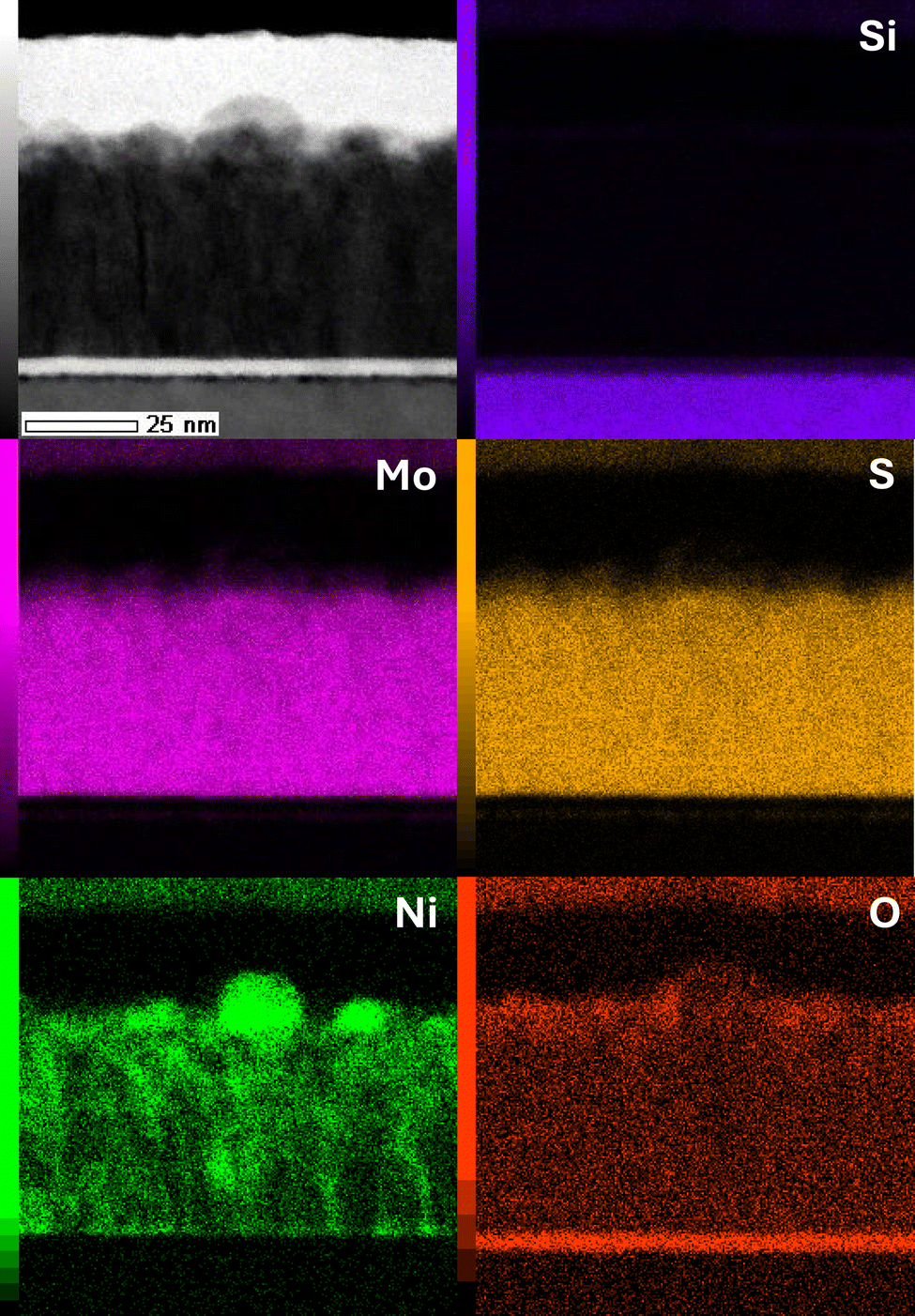 | ||
| Fig. 1 EDX maps of the MoS2–Ni(OH)2 films show the deposited nickel as particles on top of the TMD film. In addition, some nickel is diffused into the TMD film. | ||
Raman spectroscopy, carried out over six sulfurization batches, proves that the process is very repeatable and produces homogeneous films. A representative, noise-filtered spectrum is shown in Fig. 2f, while a comprehensive set of spectra is available in Fig. S4.† The main peaks, E12g at 383 cm−1 (in-plane mode) and A1g at 410 cm−1 (out-of-plane mode) correspond to bulk MoS2. This is expected as the film formed by the vertically oriented planes has a thickness of ∼100 nm according to previous studies.49,50,66 Vertical orientation is implied by the stark difference between the peak intensities.18,67,68 Furthermore, most of the measured spectra show the so-called forbidden E11g peak at around 285 cm−1, which is typically invisible for laterally oriented crystals, is now handily detected from the exposed edge planes on the topmost surface of the vertically oriented MoS2 films.69
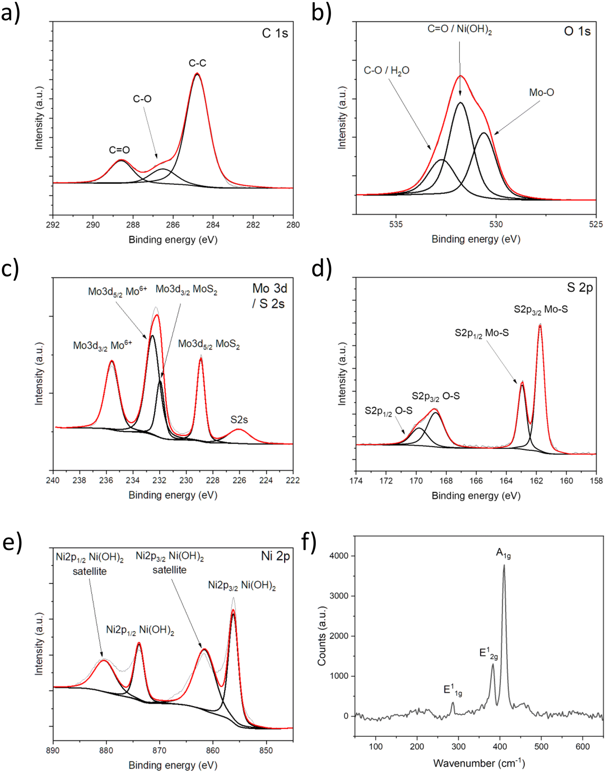 | ||
| Fig. 2 XPS (a)–(e) and Raman (f) characterization of the MoS2–Ni(OH)2 thin films. | ||
X-ray photoelectron spectroscopy (XPS) analysis is performed on a Ni decorated and annealed MoS2 sample (Fig. 2a–e) to explore the chemical composition of the surface. The C 1s peak components (Fig. 2a) indicate only adventitious carbon (C–C at 284.8 eV, C–O at 286.5 and C![[double bond, length as m-dash]](https://www.rsc.org/images/entities/char_e001.gif) O at 288.6 eV) on the surface. The resolved O 1s peak (Fig. 2b) shows Mo–O bond at 530.6 eV (indicating partial oxidation of the MoS2 lattice); CO and/or Ni(OH)2 at 531.8 eV, and C–O and/or surface water at 532.7 eV.40,70,71 Fig. 2c shows the deconvoluted Mo 3d spectrum, in which the peak at 226.1 eV is attributed to S 2s, the doublet at 228.9/232.0 eV refers to Mo4+ i.e., to MoS2, whereas the other doublet at 232.5/235.6 eV corresponds to Mo6+ i.e., to Mo–O bonds. In the S 2p spectrum (Fig. 2d), the Mo–S bond is indicated by the doublet at 161.7/162.9 eV,50,72 whereas the other two peaks at 168.7 eV and 169.8 eV are associated with oxidation products, most likely sulfate.50,73 The resolved Ni 2p spectrum (Fig. 2e) shows a doublet at 856.2 eV and 873.9 eV and corresponding satellites at 861.7 eV and 880.5 eV indicating that mostly Ni(OH)2 is present on the surface, which is reasonable considering the hydroxide peak in the O 1s spectrum at 531.8 eV.74,75 The XPS results agree with the EDX analysis, describing oxidized nickel contents on the film surface.
O at 288.6 eV) on the surface. The resolved O 1s peak (Fig. 2b) shows Mo–O bond at 530.6 eV (indicating partial oxidation of the MoS2 lattice); CO and/or Ni(OH)2 at 531.8 eV, and C–O and/or surface water at 532.7 eV.40,70,71 Fig. 2c shows the deconvoluted Mo 3d spectrum, in which the peak at 226.1 eV is attributed to S 2s, the doublet at 228.9/232.0 eV refers to Mo4+ i.e., to MoS2, whereas the other doublet at 232.5/235.6 eV corresponds to Mo6+ i.e., to Mo–O bonds. In the S 2p spectrum (Fig. 2d), the Mo–S bond is indicated by the doublet at 161.7/162.9 eV,50,72 whereas the other two peaks at 168.7 eV and 169.8 eV are associated with oxidation products, most likely sulfate.50,73 The resolved Ni 2p spectrum (Fig. 2e) shows a doublet at 856.2 eV and 873.9 eV and corresponding satellites at 861.7 eV and 880.5 eV indicating that mostly Ni(OH)2 is present on the surface, which is reasonable considering the hydroxide peak in the O 1s spectrum at 531.8 eV.74,75 The XPS results agree with the EDX analysis, describing oxidized nickel contents on the film surface.
Potential windows of the pristine MoS2 as well as MoS2–Ni(OH)2 samples are assessed from CV scans between −2 and 2 V in phosphate buffered saline (PBS), Fig. S5a.† According to the selected threshold current of ±10 μA, the feasible potential window is approximately −1 V to 1 V vs. Ag/AgCl reference. Pseudocapacitances, calculated from the difference between anodic and cathodic currents76 measured between −0.2 and 0.8 V vs. Ag/AgCl in PBS are 1 and 97 μF cm−2 for pristine MoS2 and MoS2–Ni(OH)2, respectively. Fig. S5b† also shows no discernible response for dopamine in the case of pristine MoS2, while a clear response is observed after the introduction of Ni(OH)2. Measurements using the outer sphere redox probe ferrocenemethanol were conducted to investigate the electronic properties of the electrode materials, Fig. S6.† The peak separation between the anodic and cathodic peaks suggests that the electron transfer reaction on these materials is at the slow side of quasi-reversible region and thus highly dependent on the scan rate. As the scan rate increases, the peak separation expands rapidly, reaching substantial values even at 400 mV s−1. These observations indicate slow electron transfer kinetics for these materials. The electrochemical performance of MoS2–Ni(OH)2 is assessed with a known inner sphere redox probe, dopamine. CV was initially carried out at the range of −200 to 600 mV for concentrations from 1 up to 1000 μM including the reference measurements of pristine MoS2 film (Fig. S5b†) at concentrations of 10, 100 and 1000 μM which did not produce any quantifiable response. Since the background level starts to rise from 400 mV onwards, due to the oxidation of MoS2 and Ni(OH)2 deteriorating the signal-to-noise ratio (SNR), measurements at lower concentrations (100, 200 and 500 nM) were carried out at a reduced scan range of −200 to 400 mV. Typical responses at 5, 50 and 500 μM concentrations, measured with WCEMS, are shown in Fig. 3a. The calibration curve, displayed in Fig. 3b as log–log plot of response current vs. dopamine concentration, obeys a power fit (with exponent of 0.75 ± 0.03). The statistical analysis of the measurement data is presented in Table S1.† As indicated by the error margins of statistical analysis, the reproducibility of the measurements across different samples and fabrication batches is reasonably good, especially at higher concentrations than 2 μM. The sensitivity calculated from the linear fit of sensor data in the concentration range of 0.5 to 50 μM is 0.03 μA μM−1, or 0.43 μA μM−1 cm−2 considering the area of the electrode, i.e. 0.07 cm2. The theoretical limit of detection (LOD) is estimated to be 0.1 μM or better, as determined from the standard deviation of the signal (σ ∼ 6 × 10⁻¹⁰ A) and the sensitivity value (S = 0.03 μA μM−1) according to the definition LOD = 3.3 × σ/S. The respective limit of quantification (LOQ) is one order of magnitude higher at ∼1 μM. The kinetics of the dopamine reaction exhibit characteristics of quasi-reversibility, as shown by the shift of the anodic peak potential Epa as a function of scan rate, Fig. 4a. The logarithm of the peak currents can be fitted linearly with logarithmic scan rates, Fig. S6,† with a slope of 0.47 which correlates well with the theoretical value of 0.5 for diffusion-controlled processes.
 | ||
| Fig. 3 CV data acquired with WCEMS at 5, 50 and 500 μm dopamine concentrations (a). Power function fit for the response peak currents collected jointly with Gamry and WCEMS (b). | ||
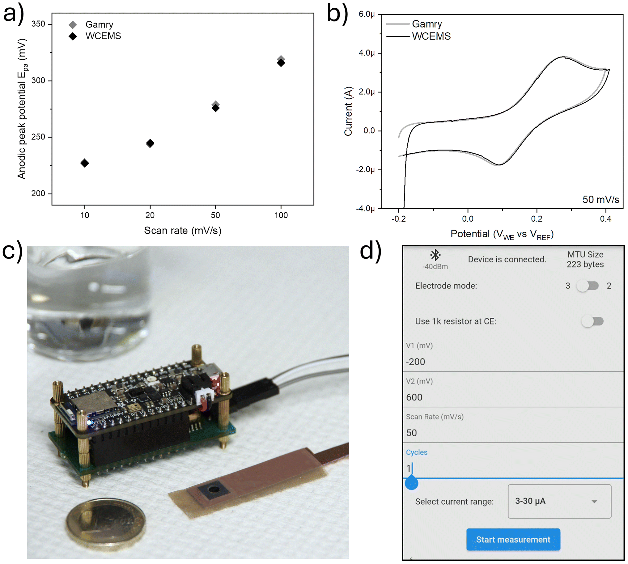 | ||
| Fig. 4 Peak potential shift with increasing scan rates at 100 μm concentration, (a) and a comparison between Gamry and WCEMS output data at the scan rate of 50 mV s−1 (b). WCEMS and a working electrode assembly with MoS2–Ni(OH)2 sample (c). 1 Euro coin as size reference. User interface running on android mobile device (d). | ||
The results show detection of dopamine in the dynamic range of 1–1000 μM. Performance is comparable to some MoS2 based composite materials, such as MoS2/PEDOT,77 metal catalysts (Table 1) apart from single-atom doped MoS2.41,43 The hydroxide groups on the material surface are expected to facilitate the redox reactions of the analyte by hydrogen bonding with dopamine as it is oxidized into dopamine-o-quinone.40 The catalytic mechanism relies on the transition of proton tunneling from diabatic to adiabatic states, resulting in a subsequent reduction in the activation energy for proton transfer.78 While a systematic shelf-life study was not performed in our work, we would like to note that the outer-sphere redox probe ferrocenemethanol measurements (Fig. S7†) were carried out on approximately 12 months old samples indicating that rapid aging of the surface under ordinary lab conditions does not seem to be of concern. Interference measurements, Fig. S8,† performed on 1, 10 and 100 mM of glucose, 0.1, 1 and 10 μM of uric acid well as 0.1, 1 and 10 mM of ascorbic acid, show no response either uric acid or glucose. In the case of ascorbic acid, a response is observed in millimolar concentrations, overlapping with dopamine peaks. However, in case of in vitro measurements that the portable design of WCEMS is well suited for, the ascorbic acid decomposes relatively fast, after which the dopamine can be effectively measured.79 All in all, the relatively slow reaction kinetics alongside large error margins in nanomolar concentrations still call for further optimization of the on-chip MoS2 films e.g. by engineering its surface chemistry with specific ligands or with co-catalyst nanomaterials that can selectively bind to analytes and facilitate improved charge transfer.80–83 Furthermore, portable measurements in realistic use cases would greatly benefit from integrated counter and reference electrodes on the sensor chip as such configuration could improve not only the signal-to-noise ratio (hence resolution and limit of detection) but also the practical use of the setup.
A comparison of back-to-back measurements performed on the same sample at dopamine concentration of 100 μM with both reference device and WCEMS is shown in Fig. 4b. Additional comparisons at different scan rates between 10 and 100 mV s−1 are collected to Fig. S9.† The background signal deviation for WCEMS defined at 500 nM concentration (Fig. S10†) is approximately σ ∼ 5.3 × 10⁻⁹ A, which sets the LOD of the device to ∼500 nM (being about five times higher than that of reference potentiostat). Therefore, in the context of the presented study, the noise level and data resolution of the WCEMS are sufficient to assess the sensitivity of the MoS2–Ni(OH)2 for dopamine. It is worth noting that due to the increased background the lowest current range (i.e., at the highest amplification) could not be used in these measurements. The jump in the beginning of the measurement data, as seen is Fig. 3 as well as Fig. S9,† is most probably caused by remaining bias in the electrochemical cell. This could be alleviated by adding a stabilization period in the software before running the voltage cycle or shorting the collector and working electrodes with an internal switch. Fig. 4c shows the WCEMS alongside a prepared working electrode and 4d depicts the user interface (UI) elements of the software. It is also important to note that the correction of the measured data was carried out on a computer (using OriginPro) according to the calibration curves, which may be also pre-processed on the smart phone in the future with a software upgrade. Furthermore, the design of the WCEMS allows for additional measurement functions such as differential and square wave voltammetries as well as chronoamperometry. The presented measurement scenario of MoS2–Ni(OH)2 in dopamine sensing did not utilize all the current ranges available, which could overestimate the noise performance at highest level of amplification. The rudimentary UI was designed to carry out the proof-of-concept measurement and has room for improvement, especially for continuous measurements and handling larger datasets.
Experimental
Materials
MoS2 thin films were produced by adopting the protocols reported previously.10,49,50 Specifically, p++ B-doped Si wafers with resistivity of <0.005 Ω cm were laser-cut halfway through from the backside into 7 × 7 mm2 square patterns with an LPKF ProtoLaser U3 (Nd:YVO4, λ = 355 nm, Pavg = 6 W, f = 40 kHz, τ = ∼20 ns, ∼20 μm focal spot diameter). The contact resistance between the substrate and TMD film was minimized by etching the native oxide layer of the Si substrate with buffered hydrofluoric acid. Immediately after etching, a thin Mo film (20 nm) was deposited by sputtering (Torr International PVD System) and the chips were subsequently sulfurized with 1 g of S powder (Sigma-Aldrich 215236, ≥95%) in a tube oven (Thermo Scientific Thermolyne with a quartz tube of 2′′ in diameter) at 800 °C under 400 sccm N2 flow for 1 hour. Each sulfurization process produced a batch of 12 sensor chips. After sulfurization, Ni with a thickness of ∼15 Å was deposited with the physical vapor deposition (PVD) system followed by annealing for 1 h at 400 °C under 400 sccm Ar flow.The structure, physical and chemical properties of similar on-chip MoS2 films have been characterized extensively in previous works,10,49,50 which is now complemented with Raman analyses of multiple sample batches to assess the stability of the sulfurization process. The cross-section lamella of the MoS2–Ni(OH)2 film was prepared with focused ion beam (FIB, FEI Helios DualBeam) and analyzed by transmission electron microscope (TEM, JEOL JEM-2200FS EFTEM/STEM) including EDX mapping. In addition, AFM (MultiMode 8, Nanoscope V, Bruker) is used to compare the surface morphology and roughness before and after the deposition of Ni and subsequent annealing. Also, XPS analysis (Thermo Fischer Scientific ESCALAB 250Xi) is carried out to understand the chemical composition of the surface after Ni decoration and annealing.
Sensor preparation and electrochemical measurements
The electrochemical sensors were prepared as follows. First, the native oxide from the backside of the chips was mechanically removed. Then, the chips were mounted on strips of copper-plated printed circuit board (PCB) using silver paste. Finally, the as-obtained structures were insulated with Teflon tape, sans a punched 3 mm diameter hole on the tape, confining the active sensor area to approximately 7 mm2. On-chip MoS2 films without deposited Ni were also prepared and measured as reference samples. These assemblies were then used as working electrodes in three-electrode configuration measurements in conjunction with a Pt wire (Sigma-Aldrich 267228, 99.9%) as counter and Ag/AgCl (in saturated KCl) as the reference electrodes (Radiometer Analytical XR300).With the exception of the 1 mM ferrocenemethanol (Thermo Scientific Chemicals, 1273-86-5, 97%) outer-sphere redox probe measurements done in 1 M KCl (Sigma-Aldrich, P3911, ≥95%), 0.01 M PBS (Sigma-Aldrich SIALP3813) was used as electrolyte in all experiments including the preparation of dopamine solutions (0.1–1000 μM, dopamine hydrochloride, Sigma-Aldrich H8502, ≥95%). CV was performed with voltage scans from −200 mV up to 400–800 mV depending on the concentration range with 3 subsequent cycles performed at a scan rate of 50 mV s−1. N2 was bubbled through the electrolyte to remove oxygen as well as to provide mixing during the measurements. A minimum of three samples were measured at each concentration for assessing statistical variation. The electrochemical results were collected using either or both Gamry Reference 600+ (Gamry Instruments, Inc.) and WCEMS devices as stated in the figure captions.
Electronics and software design of WCEMS
Adafruit Feather nRF52840 Sense (Adafruit Industries LLC) microcontroller main board was selected as the center point of the device design since it incorporates Bluetooth Low Energy (BLE) communication capabilities, reasonably small footprint and integrated Li-ion battery charger circuit in a single system. The potentiostat PCB was designed to conform with Adafruit's FeatherWing expansion card form factor and could thus be stacked with the microcontroller PCB and a Li-ion battery (400 mA h/3.7 V, Shenzhen PKCELL Battery Co., Ltd). The device dimensions are approximately 23 × 56 × 26 mm3 and weight of 28.3 g including the battery. The modular approach of the PCBs allows a clear separation between the microcontroller and potentiostat circuits, with only I/O pins, operating voltage and ground transferred between the boards. This makes it straightforward to upgrade either of the boards, as long as the form factor and pinouts are kept same. In addition, separating the radio frequency (RF) and battery charging components from the measurement circuit board can improve noise performance.The electronics design for the potentiostat circuit board (Fig. S11†) can be broken down into six sections: (1) headers for connections and power delivery between potentiostat and microcontroller PCBs. (2) 16-Bit digital-to-analog (DAC) converter with 3.0 V voltage reference (AD5663 & REF193, Analog Devices Inc.) to carry out the voltage ramps. (3) An 8-channel single-pole single-throw (SPST) switch (MAX395, Analog Devices, Inc.) controls the operation of the potentiostat, such as connecting the cell electrodes, optional 1 kΩ resistor at counter electrode to dampen oscillation and the different feedback resistors of the transimpedance amplifier. The amplifier (4) has 4 gain settings between 103 and 106 determined with precision resistors, followed by a 4th order Sallen-Key low-pass filter stage (5) with a cutoff frequency of 10 Hz. An LTspice simulation of analog signal processing stage is presented in Fig. S12.† In the end of the signal path, a 16-bit analog-to-digital (ADC) converter (6) (ADS1118, Texas Instruments Inc.) is used to quantize the signal, with optional inputs for directly sampling the digital-to-analog converter and raw transimpedance amplifier outputs as well as the virtual ground level. All operational amplifiers (i.e. used in the transimpedance amplifier, low-pass filter as well as in the feedback circuit of the electrochemical cell) are MCP6022 type (Microchip Technology Inc.). The four-layer PCB incorporates two dedicated copper layers for operating voltage and ground plane. Electronics schematic and layout are implemented with KiCad 6.0.1 EDA and made available in open data repository (Zenodo).
The microcontroller is programmed with C++ using Arduino 2.2.1 IDE (Arduino S.R.L.). The program receives initial parameters over Bluetooth low energy (BLE), executes CV measurements accordingly and sends the result data back to the control device to be displayed in the user interface. The DAC output refresh frequency is set to 200 Hz while sampling frequency of ADC is determined to be twice the cutoff frequency of the low-pass filter, i.e. 20 Hz. The implementation of CV loop is presented in ESI,† while the rest of the codebase is available in the code repository. The user interface for Android mobile device was implemented with Flutter in Visual Studio 1.85.1 IDE (Microsoft Corporation). The interface (Fig. 4d) allows for the selection of CV parameters such as voltage range, scan rate, number of cycles and desired level of amplification. The ongoing measurement can be observed in real time and the result is saved in .csv format on the device. The codebase is made available in GitHub under MIT license. Demonstration of the measurement setup and data collection is provided in the ESI† video file.
The calibration of the WCEMS is carried out by measuring CVs with a scan window between −1000 and 1000 mV with precision resistors from 1 kΩ to 1 MΩ for each amplification level. The results (Fig. S13†) are fitted in OriginPro and corrections are calculated according to the linear fit to match the desired 1000 mV output at transimpedance amplifier at maximum of the voltammetry ramp. The respective correction factors were then applied for the collected measurement data.84
Conclusions
In this study, vertically aligned MoS2 thin films modified with Ni(OH)2 were synthesized directly on Si chips and assessed as working electrodes for electrochemical sensors. AFM and XPS were carried out to investigate surface structure and chemical composition, while Raman spectroscopy verified the repeatability of the sulfurization process. The on-chip electrodes proved to be sensitive for dopamine with a dynamic current response at concentrations between 1 and 1000 μM with a theoretical limit of detection of 0.1 μM. The sensor measurements were accompanied by a custom proof-of-concept portable potentiostat design and demonstration, suitable for cyclic voltammetry measurements and wireless transmission of the data. The potentiostat performance was assessed to be comparable to the reference device in the measurements, while having the capability to perform experiments outside the laboratory. In addition, the open-source design is straightforward to modify, thus having the potential to address other measurement parameters and functions of interest. The results of this research work establish a foundation for the future development of on-chip TMD materials based electrochemical sensing and highlight the importance of incorporating co-catalyst nanomaterials to enhance electrocatalytic activity as well as to engineer chemical selectivity.Author contributions
TJ: conceptualization, software, data curation, formal analysis, validation, investigation, visualization, methodology, writing – original draft, writing – review & editing. OP: conceptualization, formal analysis, investigation, methodology, writing – review & editing. TL: conceptualization, formal analysis, validation, investigation, writing – review & editing. MM: investigation. SS: resources, supervision. KK: conceptualization, resources, formal analysis, supervision, funding acquisition, project administration, writing – review & editing.Data availability
Characterization and measurement data are available in Zenodo repository (https://doi.org/10.5281/zenodo.10808987) interlinked to a Github repository containing the WCEMS software.Conflicts of interest
There are no conflicts to declare.Acknowledgements
XPS characterization and materials synthesis was carried out with the support of the Centre for Material Analysis, University of Oulu, Finland. Tiitus Järvinen, B. Sc. (Tech.) is acknowledged for advice with the interface development in Visual Studio. The work has been partly funded by Academy of Finland (grant number 325185) and Kvantum Institute, University of Oulu (ROAR project), FARIA (UD2D project) as well as grants from Walter Ahlström, Tauno Tönning, Emil Aaltonen and Riitta and Jorma J. Takanen foundations and University of Oulu Graduate School (UniOGS).References
- A. Sebastian, R. Pendurthi, T. H. Choudhury, J. M. Redwing and S. Das, Nat. Commun., 2021, 12, 693 CrossRef PubMed.
- K. Tang, Y. Wang, C. Gong, C. Yin, M. Zhang, X. Wang and J. Xiong, Adv. Electron. Mater., 2022, 8, 2101099 CrossRef.
- J. Y. Lee, J.-H. Shin, G.-H. Lee and C.-H. Lee, Nanomaterials, 2016, 6, 193 CrossRef PubMed.
- C. Mu, J. Xiang and Z. Liu, J. Mater. Res., 2017, 32, 4115–4131 CrossRef.
- Y. Li, L. Wang, A. Song, M. Xia, Z. Li and G. Shao, Electrochim. Acta, 2018, 268, 268–275 CrossRef.
- N. Thomas, S. Mathew, K. M. Nair, K. O'Dowd, P. Forouzandeh, A. Goswami, G. McGranaghan and S. C. Pillai, Materials Today Sustainability, 2021, 13, 100073 CrossRef.
- M. S. Javed, S. Dai, M. Wang, D. Guo, L. Chen, X. Wang, C. Hu and Y. Xi, J. Power Sources, 2015, 285, 63–69 CrossRef.
- Q. Yun, L. Li, Z. Hu, Q. Lu, B. Chen and H. Zhang, Adv. Mater., 2020, 32, 1903826 CrossRef PubMed.
- Y. Huang, J. Guo, Y. Kang, Y. Ai and C. Ming Li, Nanoscale, 2015, 7, 19358–19376 RSC.
- T. Järvinen, G. S. Lorite, J. Peräntie, G. Toth, S. Saarakkala, V. K. Virtanen and K. Kordas, Nanotechnology, 2019, 30, 405501 CrossRef PubMed.
- T. H. Kim, Y. H. Kim, S. Y. Park, S. Y. Kim and H. W. Jang, Chemosensors, 2017, 5, 15 CrossRef.
- M. Pavličková, L. Lorencová, M. Hatala, M. Kováč, J. Tkáč and P. Gemeiner, Sci. Rep., 2022, 12, 11900 CrossRef.
- R. Sha and T. K. Bhattacharyya, Electrochim. Acta, 2020, 349, 136370 CrossRef CAS.
- G. Li, D. Zhang, Q. Qiao, Y. Yu, D. Peterson, A. Zafar, R. Kumar, S. Curtarolo, F. Hunte, S. Shannon, Y. Zhu, W. Yang and L. Cao, J. Am. Chem. Soc., 2016, 138, 16632–16638 CrossRef CAS.
- H. Schweiger, P. Raybaud, G. Kresse and H. Toulhoat, J. Catal., 2002, 207, 76–87 CrossRef CAS.
- A. Sinha, Dhanjai, B. Tan, Y. Huang, H. Zhao, X. Dang, J. Chen and R. Jain, Trends Anal. Chem., 2018, 102, 75–90 CrossRef CAS.
- S. M. Ahmed and H. Gerischer, Electrochim. Acta, 1979, 24, 705–711 CrossRef CAS.
- S. M. Tan, A. Ambrosi, Z. Sofer, Š. Huber, D. Sedmidubský and M. Pumera, Chem.–Eur. J., 2015, 21, 7170–7178 CrossRef CAS.
- P. Song, P. Ou, Y. Wang, H. Yuan, S. Duan, L. Chen, H. Fu, J. Song and X. Liu, Anal. Chim. Acta, 2023, 1252, 341036 CrossRef CAS.
- M. Cantarella, G. Gorrasi, A. Di Mauro, M. Scuderi, G. Nicotra, R. Fiorenza, S. Scirè, M. E. Scalisi, M. V. Brundo, V. Privitera and G. Impellizzeri, Sci. Rep., 2019, 9, 974 CrossRef PubMed.
- J. N. Coleman, M. Lotya, A. O'Neill, S. D. Bergin, P. J. King, U. Khan, K. Young, A. Gaucher, S. De, R. J. Smith, I. V. Shvets, S. K. Arora, G. Stanton, H.-Y. Kim, K. Lee, G. T. Kim, G. S. Duesberg, T. Hallam, J. J. Boland, J. J. Wang, J. F. Donegan, J. C. Grunlan, G. Moriarty, A. Shmeliov, R. J. Nicholls, J. M. Perkins, E. M. Grieveson, K. Theuwissen, D. W. McComb, P. D. Nellist and V. Nicolosi, Science, 2011, 331, 568–571 CrossRef CAS.
- L. Durai, C. Y. Kong and S. Badhulika, Mater. Sci. Eng., C, 2020, 107, 110217 CrossRef CAS PubMed.
- C. Nagaraju, C. V. V. M. Gopi, J.-W. Ahn and H.-J. Kim, New J. Chem., 2018, 42, 12357–12360 RSC.
- D. Wang, Z. Pan, Z. Wu, Z. Wang and Z. Liu, J. Power Sources, 2014, 264, 229–234 CrossRef CAS.
- H. Samassekou, A. Alkabsh, M. Wasala, M. Eaton, A. Walber, A. Walker, O. Pitkänen, K. Kordas, S. Talapatra, T. Jayasekera and D. Mazumdar, 2D Mater., 2017, 4, 021002 CrossRef.
- Y.-H. Lee, X.-Q. Zhang, W. Zhang, M.-T. Chang, C.-T. Lin, K.-D. Chang, Y.-C. Yu, J. T.-W. Wang, C.-S. Chang, L.-J. Li and T.-W. Lin, Adv. Mater., 2012, 24, 2320–2325 CrossRef CAS PubMed.
- J. Zhang, H. Yu, W. Chen, X. Tian, D. Liu, M. Cheng, G. Xie, W. Yang, R. Yang, X. Bai, D. Shi and G. Zhang, ACS Nano, 2014, 8, 6024–6030 CrossRef CAS.
- Y. Jung, J. Shen, Y. Liu, J. M. Woods, Y. Sun and J. J. Cha, Nano Lett., 2014, 14, 6842–6849 CrossRef CAS PubMed.
- D. Kong, H. Wang, J. J. Cha, M. Pasta, K. J. Koski, J. Yao and Y. Cui, Nano Lett., 2013, 13, 1341–1347 CrossRef.
- R. Sha, N. Vishnu and S. Badhulika, Sens. Actuators, B, 2019, 279, 53–60 CrossRef CAS.
- Y. J. Zhai, J. H. Li, X. Y. Chu, M. Z. Xu, F. J. Jin, X. Li, X. Fang, Z. P. Wei and X. H. Wang, J. Alloys Compd., 2016, 672, 600–608 CrossRef CAS.
- L. Fang, F. Wang, Z. Chen, Y. Qiu, T. Zhai, M. Hu, C. Zhang and K. Huang, Talanta, 2017, 167, 593–599 CrossRef CAS PubMed.
- R. Žalnėravičius, A. Gedminas, T. Ruzgas and A. Jagminas, J. Electroanal. Chem., 2019, 839, 274–282 CrossRef.
- J. Zhou, Y. Zhao, J. Bao, D. Huo, H. Fa, X. Shen and C. Hou, Electrochim. Acta, 2017, 250, 152–158 CrossRef CAS.
- G. Jeevanandham, R. Jerome, N. Murugan, M. Preethika, K. Vediappan and A. K. Sundramoorthy, RSC Adv., 2020, 10, 643–654 RSC.
- S. Li, Y. Ma, Y. Liu, G. Xin, M. Wang, Z. Zhang and Z. Liu, RSC Adv., 2019, 9, 2997–3003 RSC.
- Y. Zhao, J. Zhou, Z. Jia, D. Huo, Q. Liu, D. Zhong, Y. Hu, M. Yang, M. Bian and C. Hou, Microchim. Acta, 2019, 186, 92 CrossRef.
- D. Sarkar, W. Liu, X. Xie, A. C. Anselmo, S. Mitragotri and K. Banerjee, ACS Nano, 2014, 8, 3992–4003 CrossRef CAS.
- A. M. Parra-Alfambra, E. Casero, L. Vázquez, C. Quintana, M. del Pozo and M. D. Petit-Domínguez, Sens. Actuators, B, 2018, 274, 310–317 CrossRef CAS.
- A. M. Tomy, B. Sathyan and J. Cyriac, J. Electrochem. Soc., 2023, 170, 047506 CrossRef CAS.
- X. Sun, C. Chen, C. Xiong, C. Zhang, X. Zheng, J. Wang, X. Gao, Z.-Q. Yu and Y. Wu, Nano Res., 2023, 16, 917–924 CrossRef CAS.
- L. Ma, Q. Zhang, C. Wu, Y. Zhang and L. Zeng, Anal. Chim. Acta, 2019, 1055, 17–25 CrossRef CAS.
- Y. Lei, D. Butler, M. C. Lucking, F. Zhang, T. Xia, K. Fujisawa, T. Granzier-Nakajima, R. Cruz-Silva, M. Endo, H. Terrones, M. Terrones and A. Ebrahimi, Sci. Adv., 2020, 6, eabc4250 CrossRef CAS.
- S. Su, H. Sun, F. Xu, L. Yuwen and L. Wang, Electroanalysis, 2013, 25, 2523–2529 CrossRef CAS.
- J. Huang, Y. He, J. Jin, Y. Li, Z. Dong and R. Li, Electrochim. Acta, 2014, 136, 41–46 CrossRef CAS.
- D. Geng, X. Bo and L. Guo, Sens. Actuators, B, 2017, 244, 131–141 CrossRef CAS.
- Y. Yang, J. Zhang, Y. W. Li, Q. Shan and W. Wu, Colloids Surf., A, 2021, 625, 126865 CrossRef CAS.
- Z. Dourandish, I. Sheikhshoaie and S. Maghsoudi, Biosensors, 2023, 13, 524 CrossRef CAS PubMed.
- T. Järvinen, H.-P. Komsa and K. Kordas, AIP Adv., 2020, 10, 065114 CrossRef.
- T. Järvinen, S.-H. H. Shokouh, S. Sainio, O. Pitkänen and K. Kordas, Nanoscale Adv., 2022, 4, 3243–3249 RSC.
- N. O. Gomes, S. C. Teixeira, M. L. Calegaro, S. A. S. Machado, N. de Fátima Ferreira Soares, T. V. de Oliveira and P. A. Raymundo-Pereira, Chem. Eng. J., 2023, 472, 144775 CrossRef CAS.
- A. A. Rowe, A. J. Bonham, R. J. White, M. P. Zimmer, R. J. Yadgar, T. M. Hobza, J. W. Honea, I. Ben-Yaacov and K. W. Plaxco, PLoS One, 2011, 6, e23783 CrossRef CAS.
- K. Xu, Q. Chen, Y. Zhao, C. Ge, S. Lin and J. Liao, Sens. Actuators, B, 2020, 319, 128221 CrossRef CAS.
- M. D. M. Dryden and A. R. Wheeler, PLoS One, 2015, 10, e0140349 CrossRef PubMed.
- A. Das, S. Bose, N. Mandal, B. Pramanick and C. RoyChaudhuri, Proc. Indian Natl. Sci. Acad., 2021, 87, 84–93 Search PubMed.
- A. Ainla, M. P. S. Mousavi, M.-N. Tsaloglou, J. Redston, J. G. Bell, M. T. Fernández-Abedul and G. M. Whitesides, Anal. Chem., 2018, 90, 6240–6246 CrossRef CAS PubMed.
- K. Krorakai, S. Klangphukhiew, S. Kulchat and R. Patramanon, Appl. Sci., 2021, 11, 392 CrossRef CAS.
- S. Sarkar and M. Bhattacharya, in IECON 2020 The 46th Annual Conference of the IEEE Industrial Electronics Society, 2020, pp. 5249–5254 Search PubMed.
- A. Nemiroski, D. C. Christodouleas, J. W. Hennek, A. A. Kumar, E. J. Maxwell, M. T. Fernández-Abedul and G. M. Whitesides, Proc. Natl. Acad. Sci. U.S.A., 2014, 111, 11984–11989 CrossRef CAS PubMed.
- T. Tichter, M. Gernhard and P. C. K. Vesborg, Electrochim. Acta, 2023, 469, 143119 CrossRef CAS.
- M. Caux, A. Achit, K. Var, G. Boitel-Aullen, D. Rose, A. Aubouy, S. Argentieri, R. Campagnolo and E. Maisonhaute, HardwareX, 2022, 11, e00290 CrossRef PubMed.
- Y. Matsubara, J. Chem. Educ., 2021, 98, 3362–3370 CrossRef CAS.
- C. Grazioli, E. Lanza, M. Abate, G. Bontempelli and N. Dossi, Talanta, 2024, 275, 126185 CrossRef CAS.
- D. M. Jenkins, B. E. Lee, S. Jun, J. Reyes-De-Corcuera and E. S. McLamore, J. Electrochem. Soc., 2019, 166, B3056 CrossRef CAS.
- R. Ahmad, S. G. Surya, J. Batista Sales, H. Mkaouar, S. Y. Cavalcanti Catunda, D. Rodrigues Belfort, Y. Lei, Z. L. Wang, A. Baeumner, O. S. Wolfbeis, H. N. Alshareef and K. N. Salama, in 2019 IEEE SENSORS, 2019, pp. 1–4 Search PubMed.
- H. Li, Q. Zhang, C. C. R. Yap, B. K. Tay, T. H. T. Edwin, A. Olivier and D. Baillargeat, Adv. Funct. Mater., 2012, 22, 1385–1390 CrossRef CAS.
- Y. Yang, H. Fei, G. Ruan, C. Xiang and J. M. Tour, Adv. Mater., 2014, 26, 8163–8168 CrossRef CAS PubMed.
- J. L. Verble and T. J. Wieting, Phys. Rev. Lett., 1970, 25, 362–365 CrossRef.
- Y. Guo, W. Zhang, H. Wu, J. Han, Y. Zhang, S. Lin, C. Liu, K. Xu, J. Qiao, W. Ji, Q. Chen, S. Gao, W. Zhang, X. Zhang and Y. Chai, Sci. Adv., 2018, 4, eaau6252 CrossRef PubMed.
- H. Liu, X. Chen, L. Deng, M. Ding, J. Li and X. He, J. Mater. Chem. A, 2016, 4, 17764–17772 RSC.
- S. Yamamoto, T. Kendelewicz, J. T. Newberg, G. Ketteler, D. E. Starr, E. R. Mysak, K. J. Andersson, H. Ogasawara, H. Bluhm, M. Salmeron, G. E. Brown Jr and A. Nilsson, J. Phys. Chem. C, 2010, 114, 2256–2266 CrossRef.
- B. Zhang, J. Liu, J. Wang, Y. Ruan, X. Ji, K. Xu, C. Chen, H. Wan, L. Miao and J. Jiang, Nano Energy, 2017, 37, 74–80 CrossRef.
- H. Liu, H. Hu, J. Wang, P. Niehoff, X. He, E. Paillard, D. Eder, M. Winter and J. Li, ChemElectroChem, 2016, 3, 922–932 CrossRef.
- A. P. Grosvenor, M. C. Biesinger, R. St. C. Smart and N. S. McIntyre, Surf. Sci., 2006, 600, 1771–1779 CrossRef.
- E. S. Lambers, C. N. Dykstal, J. M. Seo, J. E. Rowe and P. H. Holloway, Oxid. Met., 1996, 45, 301–321 CrossRef.
- T. Laurila, V. Protopopova, S. Rhode, S. Sainio, T. Palomäki, M. Moram, J. M. Feliu and J. Koskinen, Diamond Relat. Mater., 2014, 49, 62–71 CrossRef.
- Y. Li, H. Lin, H. Peng, R. Qi and C. Luo, Microchim. Acta, 2016, 183, 2517–2523 CrossRef.
- R. E. Warburton, A. V. Soudackov and S. Hammes-Schiffer, Chem. Rev., 2022, 122, 10599–10650 CrossRef PubMed.
- S. Rantataro, L. Ferrer Pascual and T. Laurila, Sci. Rep., 2022, 12, 20225 CrossRef PubMed.
- R. C. de Freitas, W. T. Fonseca, D. C. Azzi, P. A. Raymundo-Pereira, O. N. Oliveira and B. C. Janegitz, Microchem. J., 2023, 191, 108823 CrossRef CAS.
- T. C. Canevari, P. A. Raymundo-Pereira, R. Landers, E. V. Benvenutti and S. A. S. Machado, Talanta, 2013, 116, 726–735 CrossRef CAS PubMed.
- S. Chumillas, T. Palomäki, M. Zhang, T. Laurila, V. Climent and J. M. Feliu, Electrochim. Acta, 2018, 292, 309–321 CrossRef CAS.
- S. Sainio, E. Leppänen, E. Mynttinen, T. Palomäki, N. Wester, J. Etula, N. Isoaho, E. Peltola, J. Koehne, M. Meyyappan, J. Koskinen and T. Laurila, Mol. Neurobiol., 2020, 57, 179–190 CrossRef CAS PubMed.
- A. W. Colburn, K. J. Levey, D. O'Hare and J. V. Macpherson, Phys. Chem. Chem. Phys., 2021, 23, 8100–8117 RSC.
Footnote |
| † Electronic supplementary information (ESI) available: WCEMS schematics, simulations, calibrations, reference measurements, cyclic voltammetry function and demonstration video of the user interface. AFM, EDX, TEM image and Raman of the thin films. See DOI: https://doi.org/10.1039/d4na00914b |
| This journal is © The Royal Society of Chemistry 2025 |