
 Open Access Article
 This Open Access Article is licensed under a
 Creative Commons Attribution 3.0 Unported Licence
Monodisperse spherical Ag+ doped Cs2KBiCl6 nanocrystals: utilizing steric hindrance engineering for inkjet printing of anti-counterfeiting patterns†
Shaoli Songa,
Youlun Zhua,
Hanmei Jianga,
Huichao He a,
Qian Yanga,
Jianbei Qiub and
Tao Han*a
a,
Qian Yanga,
Jianbei Qiub and
Tao Han*a
aCollege of Materials and New Energy, Chongqing University of Science and Technology, Chongqing, 401331, China. E-mail: danbaiht@126.com
bSchool of Materials Science and Engineering, Kunming University of Science and Technology, Kunming, Yunnan 650093, P. R. China
First published on 6th May 2025
Abstract
Anti-counterfeiting is one of the critical application fields of luminescent materials. Nanocrystal luminescent materials are more suitable for anti-counterfeiting applications because they are tiny and more conducive to patterning. The preparation of monodisperse and spherical lead-free perovskite nanocrystals by a propagable method is a hot topic in anti-counterfeiting materials. In this work, monodisperse spherical Ag+ doped Cs2KBiCl6 nanocrystals with an average diameter of 3.51 nm were prepared by using the propagable ligand-assisted reprecipitation method at room temperature, attributed to steric hindrance engineering by increasing the ligand size. Due to relaxation of the transition barrier due to doping, excited with 365 nm ultraviolet light, the nanocrystals exhibit orange emission peaking at 600 nm, which is related to the transition recombination of Bi3+ (1S0 → 3P1), and the maximum photoluminescence quantum yield is 3.80%. A printable ink is prepared by combining the nanocrystals with PDMS adhesive and its curing agent, which can be used for inkjet printing of anti-counterfeiting patterns.
1 Introduction
The patterning of luminescent materials is a vital part of its application in anti-counterfeiting.1–5 Compared with micron-sized crystal luminescent materials, nanocrystalline luminescent materials are more suitable for patterning due to their tiny size.6–10 Combining nanocrystal luminescent materials with organic solvents to prepare printable inks has been proven to be a reliable solution for their patterning.11 At present, the popular nanocrystal luminescent materials for anti-counterfeiting are lead halide perovskite nanocrystals prepared by the hot injection method. However, the hot injection method has the following disadvantages: the obtained nanocrystals are usually square and poorly dispersed, which is not conducive to inkjet printing; rigorous environmental conditions are required including high temperature (100–200 °C), no oxygen, and no water.12 In addition, the toxicity of lead limits its application in the field of anti-counterfeiting.13–17 Therefore, the monodisperse spherical lead-free perovskite nanocrystals will play an important role in the field of anti-counterfeiting.The spray method has been considered as an alternative to the thermal injection method,18–20 but it has not been widely used because of its high cost, adverse environmental impact and difficulty in controlling the size distribution of the prepared nanocrystals. In comparison with the hot injection method, the ligand-assisted reprecipitation method at room temperature can produce nanocrystals with good dispersion degrees and regular shapes. In 2016, Li21 et al. first prepared colloidal nanocrystals by ligand-assisted reprecipitation. The morphology of nanocrystals can be controlled in the process of reprecipitation by transforming organic acids and amine ligands.22 Additionally, toxic organic acids and amines can be replaced with the non-toxic K30 polyvinylpyrrolidone (PVP).23 However, the agglomeration of nanocrystals is still a problem that hinders their application.
Furthermore, the substitution of Pb2+ with a monovalent metal cation (Na+, K+, and Ag+) and a trivalent metal cation (Bi3+ and In3+) is the main strategy, which can maintain the perovskite structure without disrupting the charge balance and also replace the toxic lead element. Recently, lead-free double perovskite nanocrystals have become a hot research topic in the field of luminescent materials.24–31
In the present work, spherical Ag+ doped Cs2KBiCl6 nanocrystals were prepared by a generalized ligand-assisted reprecipitation method at room temperature using non-toxic K60 PVP as the ligand. This method is energy-efficient and environmentally friendly. Because of the steric hindrance effect ascribed to the considerable molecular weight (220![[thin space (1/6-em)]](https://www.rsc.org/images/entities/char_2009.gif) 000) of K60 PVP, the prepared nanocrystals have good dispersion. The spherical and well-dispersed nanocrystals are easier to inkjet print. The doped silver creates spatially localized electron and hole states in the crystal,32 which lowers the transition barrier of Bi3+ (1S0 → 3P1), and exhibits an orange emission centered at 600 nm under the excitation of 365 nm ultraviolet light. Due to their good dispersion, spherical shape and nanoscale size, the obtained Cs2KBiCl6 nanocrystals are suitable for inkjet printing anti-counterfeiting patterns. The dispersed spherical Ag+ doped Cs2KBiCl6 nanocrystals were blended with PDMS adhesive and its curing agent to produce a printable ink, which can be used for inkjet printing of anti-counterfeiting patterns.
000) of K60 PVP, the prepared nanocrystals have good dispersion. The spherical and well-dispersed nanocrystals are easier to inkjet print. The doped silver creates spatially localized electron and hole states in the crystal,32 which lowers the transition barrier of Bi3+ (1S0 → 3P1), and exhibits an orange emission centered at 600 nm under the excitation of 365 nm ultraviolet light. Due to their good dispersion, spherical shape and nanoscale size, the obtained Cs2KBiCl6 nanocrystals are suitable for inkjet printing anti-counterfeiting patterns. The dispersed spherical Ag+ doped Cs2KBiCl6 nanocrystals were blended with PDMS adhesive and its curing agent to produce a printable ink, which can be used for inkjet printing of anti-counterfeiting patterns.
2 Experimental
2.1 Raw materials
Cesium chloride (CsCl, 99.99%), potassium chloride (KCl, 99.99%), bismuth acetate (C6H9BiO6, 99.99%), silver acetate (C2H3O2Ag, 99.95%), N,N-dimethylformamide (C3H7NO, 99.9%), and isopropanol (C3H8O, 99.9%) were purchased from Aladdin, K60-type polyvinylpyrrolidone ((C6H9NO)n, average molecular weight 220000) was purchased from Macklin, and hydrochloric acid (HCl, 36%) was purchased from Chengdu Kelong Chemical. All chemicals were used as is.
2.2 Ag+ doping Cs2KBiCl6 synthesis of nanocrystals (using Cs2K0.95Ag0.05BiCl6 as an example)
Ag+ doped Cs2KBiCl6 nanocrystals were synthesized by a ligand-assisted reprecipitation method at room temperature. Typically, 2 mmol of CsCl, 0.95 mmol of kCl, 0.05 mmol of C2H3O2Ag, 1 mmol of C6H9BiO6, and 1 g of K60 PVP were dissolved in a solvent mixture including 100 ml of DMF, 20 ml of purified water, and 5 ml of concentrated hydrochloric acid, and then stirred at room temperature for about 1 h. After the reactants had completely dissolved, the above solution was injected into 375 ml of stirring isopropyl alcohol and stirred for about 10 min. The resulting turbid liquid was centrifuged at 8000 rpm for 5 min, the sediment was retained, and then the precipitate was re-dispersed in 5 ml of isopropanol.2.3 Preparation of ink and inkjet printing of anti-counterfeiting patterns
5 ml of Cs2K0.95Ag0.05BiCl6 nanocrystal dispersion (concentration: 0.4 mmol ml−1) was mixed with 5 ml of PDMS (Brand D, model: DC184) glue and 0.5 ml of curing agent. Then the mixture is thoroughly stirred to ensure uniform dispersion and placed in an oven and heat at 100 °C for 3 hours, which is crucial to achieve the desired viscosity and printability of the ink. Then the prepared printable ink was transferred into the printing needle tubing of a high-viscosity paste direct writing micro-electronic printer (Brand V) and loaded without any air bubbles or contamination. Then, the desired pattern was selected to be printed and the printing parameters were carefully set on the printer's control panel, which is vital for achieving accurate and precise printing. Then, the inkjet printing process was carried out, depositing the ink onto the base material (glass) according to the selected pattern and printing parameters. Then, the printed glass substrate was placed in an oven and baked at 100 °C for 15 hours.2.4 Characterization
The XRD patterns of the samples were collected on a TD-3500 X-ray diffractometer (SmartLab, Rigaku, Japan) using a Cu Kα radiation source (λ = 1.5406) with an operating voltage of 30 kV and a tube current of 20 mA. The elemental composition of the sample was measured using inductively coupled plasma mass spectrometry (Agilent 5110, USA). TEM images were taken on a transmission electron microscope (JEM-2100F, Jeol, Japan). The absorption spectra of the samples in the range of 200–600 nm were recorded using a UV-VIS-NIR spectrophotometer (UH5700, Hitachi, Japan). The photoluminescence (PL) and excitation spectra were recorded on a spectrophotometer (F-7000, Hitachi, Japan). PL decay lifetime and fluorescence quantum yield (PLQY) were determined on a fluorescence spectrometer (FLS980, Edinburgh, UK).3 Results and discussion
A model of the silver doped Cs2KBiCl6 double-perovskite structure is shown in Fig. 1a. In this structure, [KCl6]3− and [BiCl6]3− octahedra form a three-dimensional structure, with Cs atoms occupying the interstices of the octahedra, which contributes to structural stability. Silver ions are doped to substitute potassium ions. The X-ray diffraction patterns of the Cs2KBiCl6 and Ag+-doped Cs2KBiCl6 nanocrystals are presented in Fig. 1b. As the doping level of silver ions increases, the XRD diffraction peak exhibits a maximum leftward shift of 0.18°, indicating a slight expansion of the lattice spacing due to doping. This may be attributed to the fact that the lattice spacing expansion caused by vacancy defects and structural distortions induced by doping counteracts the lattice spacing contraction resulting from the substitution of potassium ions by silver ions. The following table presents the actual doping amounts of silver element in the samples, as determined by ICP analysis (Table 1). | ||
| Fig. 1 (a) Crystal structure of silver ion doped Cs2KBiCl6. (b) XRD patterns of Cs2K1−xAgxBiCl6 (x = 0, 0.005, 0.015, 0.036, 0.046) nanocrystals. (c) Photos of Cs2K1−xAgxBiCl6 (x = 0, 0.005, 0.015, 0.036, 0.046) nanocrystal dispersion liquid under natural light. (d) Photos of Cs2K1−xAgxBiCl6 (x = 0, 0.005, 0.015, 0.036, 0.046) nanocrystal dispersion liquid under ultraviolet light. | ||
| Sample no. | Silver ion mass fraction | Silver ion substance fraction |
|---|---|---|
| 1 | 0.00% | 0.0% |
| 2 | 0.07% | 0.5% |
| 3 | 0.22% | 1.5% |
| 4 | 0.53% | 3.6% |
| 5 | 0.68% | 4.6% |
The prepared Cs2KBiCl6 and Ag+-doped Cs2KBiCl6 nanocrystals appear white under natural light (Fig. 1c). The Cs2KBiCl6 nanocrystals do not exhibit any considerable luminescence under 365 nm ultraviolet (UV) excitation, whereas the Ag+-doped Cs2KBiCl6 nanocrystals show the orange emission under the same excitation conditions (Fig. 1d).
Herein, K16 PVP (molecular weight: 8000), K30 PVP (molecular weight: 58000) and K60 PVP (molecular weight: 220000) were used as ligands. The Cs2KBiCl6 nanocrystals were synthesised under the same concentration (1 g mmol−1 matrix). Further, the dispersion degree of nanocrystals was compared, as shown in Fig. 2a–c. Increasing the molecular weight of PVP improved the dispersion of nanocrystals, because PVP prevents nanoparticle aggregation through repulsion induced by its hydrophobic carbon chains that extend into solvents and interact with them, which belong to a steric hindrance effect. Therefore, an increase in the molecular weight of PVP likely intensifies this steric hindrance effect, improving the nanoparticle dispersion degree.
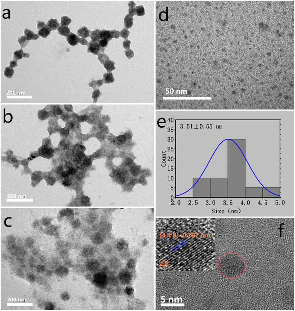 | ||
| Fig. 2 (a–c) TEM images of nanocrystals prepared using different ligands with molecular weights of 8000, 58000 and 220000, respectively. (d) Amplified TEM images of Cs2K0.954Ag0.046BiCl6 nanocrystals. (e) Size distribution of Cs2K0.954Ag0.046BiCl6 nanocrystals. (f) High-resolution TEM image of a Cs2K0.954Ag0.046BiCl6 nanocrystal. | ||
Fig. 2d shows the transmission electron microscopy (TEM) images of Cs2K0.954Ag0.046BiCl6 nanocrystals. These nanocrystals exhibit an excellent dispersion degree and a spherical morphology. Their mean diameter is 3.51 nm, with a standard deviation of 0.55 nm (Fig. 2e). The high-resolution TEM analysis of the Cs2K0.954Ag0.046BiCl6 nanocrystals reveals highly crystalline lattice fringes and a lattice spacing of 0.197 nm, which is slightly larger than the lattice spacing of the (4 4 0) crystal faces of Cs2KBiCl6 nanocrystals (0.196 nm) (Fig. 2f).
Fig. 3a presents the absorption spectra of the Cs2KBiCl6 and Ag+-doped Cs2KBiCl6 nanocrystals. The absorption peak at 335 nm observed for the Cs2KBiCl6 nanocrystals is attributed to the 6s2 → 6s1p1 transition of Bi3+ within [BiCl6]3−. The absorption intensity increases gradually with the Ag+ doping amount, accompanied by a red shift of the absorption peaking from 335 to 340 nm. In this study, the optical band gap of the Cs2KBiCl6 nanocrystals was determined using the absorption spectra and Tauc's formula, which is given below.
| (αℏν)n = A(ℏν − Eg), | (1) |
 | ||
| Fig. 3 (a) UV-Vis absorption spectra of Cs2K1−xAgxBiCl6 (x = 0, 0.005, 0.015, 0.036, 0.046) nanocrystals. (b) Tauc diagram of Cs2KBiCl6 nanocrystals. (c) PLE spectra of Cs2K1−xAgxBiCl6 (x = 0, 0.005, 0.015, 0.036, 0.046) nanocrystals. (d) PL spectra of Cs2K1−xAgxBiCl6 (x = 0, 0.005, 0.015, 0.036, 0.046) nanocrystals. (e) PLQY values of Cs2K1−xAgxBiCl6 (x = 0, 0.005, 0.015, 0.036, 0.046) nanocrystals. (f) Photoluminescence attenuation scatter plot of Cs2K1−xAgxBiCl6 (x = 0, 0.005, 0.015, 0.036, 0.046) nanocrystals. | ||
The photoluminescence excitation (PLE) spectra of Cs2KBiCl6 nanocrystals were monitored at 600 nm, exhibiting a characteristic excitation peaking at 365 nm due to the 1S0 → 3P1 transition of Bi3+. For the Ag+-doped Cs2KBiCl6 nanocrystals, this excitation peak is red-shifted to 370 nm, as shown in Fig. 3c. Under 365 nm UV excitation (Fig. 3d), the Cs2KBiCl6 and Ag+-doped Cs2KBiCl6 nanocrystals exhibit orange emission peaking at 600 nm, which arises from the self-trapped exciton emission of [BiCl6]3−, attributed to the 3P1 → 1S0 transition of Bi3+. The emission intensity gradually increases with an increase in the Ag+ doping amount, aligning with the trend that Ag+ doping substantially increases the fluorescence quantum yield of the Cs2KBiCl6 nanocrystals. The fluorescence quantum yield of undoped Cs2KBiCl6 nanocrystals is 0.04%. In contrast, for the Cs2KBiCl6 nanocrystals doped with 0.5%, 1.5%, 3.6%, and 4.6% Ag+, the fluorescence quantum yields are 1.02%, 1.27%, 3.10% and 3.80%, respectively, which represents an increase in the fluorescence quantum yield by a factor of up to 94 times with doping, as shown in Fig. 3e. The 3P1 → 1S0 transition of Bi3+ is forbidden in the Cs2KBiCl6 nanocrystals, leading to an extremely low carrier concentration upon UV excitation, which results in an extremely low fluorescence quantum yield. After silver doping, spatially localized electron and hole states are generated in the crystal, which relax the transition barrier,31 considerably augmenting the carrier concentration under UV excitation and thus substantially increasing the fluorescence quantum yield. As the Ag+ doping amount increases, the relaxation of inhibitions is more obvious, increasing the success rate of the transition. This increases the carrier concentration within the nanocrystal under UV excitation, further augmenting the fluorescence quantum yield.
The luminescence decay curves of the Cs2KBiCl6 and Ag+-doped Cs2KBiCl6 nanocrystals are shown in Fig. 3f. These decay curves were fitted with a double exponential function.
|
I(t) = A1exp(−t/τ1) + A2exp(−t/τ2),
| (2) |
| τave = (A1τ12 + A2τ22)/(A1τ1 + A2τ2), | (3) |
 | ||
| Fig. 4 (a) Diagram of the printing process. (b–j) The panda, tiger, and “50” patterns under natural light on a white background, under natural light on a black background, and under ultraviolet light on a black background. | ||
The nanocrystals synthesised in this investigation exhibit distinct colours when exposed to ultraviolet and visible light, rendering them suitable for applications requiring anti-counterfeiting capabilities. A printable ink imbued with anti-counterfeiting properties was formulated by amalgamating Cs2K0.954Ag0.046BiCl6 nanocrystals, which were prepared utilising D brand PDMS adhesive alongside its corresponding curing agent. The schematic representation of this process is depicted in Fig. 4a. Fig. 4b–4j illustrate the printed patterns as observed under varying conditions: the panda, tiger, and “50” patterns under natural light on a white background, under natural light on a black background, and under ultraviolet light on a black background.
4 Conclusion
In summary, a generalised ligand-assisted reprecipitation technique was employed at ambient temperature, wherein steric hindrance engineering was utilised to optimise the dispersion characteristics of nanocrystals through the variation of ligand types, resulting in the synthesis of spherical Ag+-doped Cs2KBiCl6 nanocrystals, which maintained an identical double perovskite structure and exhibited excellent dispersibility. The Cs2K0.954Ag0.046BiCl6 nanocrystals possessed an average diameter of 3.51 nm. Excited with 365 nm ultraviolet light, the nanocrystals exhibit orange emission peaking at 600 nm, with a fluorescence quantum yield of 3.80%. Subsequently, the nanocrystals were integrated with PDMS adhesive and its corresponding curing agent to formulate a printable ink, which is suitable for inkjet printing of anti-counterfeiting patterns.Data availability
Additional experimental data supporting this article are provided in the ESI.† Reasonable requests for additional information can be made to the corresponding author.Conflicts of interest
There are no conflicts to declare.Acknowledgements
This work is supported by the National Natural Science Foundation of China (Grant No. 12174042), Technology Innovation and Application Development Key Project of Chongqing (Grant No. CSTB2022TIAD-KPX0019), Research Project of Chongqing University of Science and Technology (Grant No. ckrc20231208), and Scientific and Technological Research Program of Chongqing Municipal Education Commission (Grant No. KJQN202101505).References
- V. P. Schnee, C. J. Bright and E. C. Nallon, et al., Contact printing of a quantum dot and polymer cross-reactive array sensor, Sens. Actuators, B, 2016, 236, 506–511 CrossRef CAS.
- B. Bangalore Rajeeva, L. Lin and E. P. Perillo, et al., High-resolution bubble printing of quantum dots, ACS Appl. Mater. Interfaces, 2017, 9(19), 16725–16733 CrossRef CAS PubMed.
- B. B. Rajeeva, M. A. Alabandi and L. Lin, et al., Patterning and fluorescence tuning of quantum dots with haptic-interfaced bubble printing, J. Mater. Chem. C, 2017, 5(23), 5693–5699 RSC.
- L. Shi, L. Meng and F. Jiang, et al., In situ inkjet printing strategy for fabricating perovskite quantum dot patterns, Adv. Funct. Mater., 2019, 29(37), 1903648 CrossRef.
- D. Li, J. Wang and M. Li, et al., Inkjet printing matrix perovskite quantum dot light-emitting devices, Adv. Mater. Technol., 2020, 5(6), 2000099 CrossRef CAS.
- J. Bae, S. Kim and J. Ahn, et al., Nanoscale 3D printing of quantum dots on paper, Adv. Eng. Mater., 2021, 23(9), 2100339 CrossRef CAS.
- J. Yang, J. Yoo and W. S. Yu, et al., Polymer-assisted high-resolution printing techniques for colloidal quantum dots, Macromol. Res., 2021, 29(6), 391–401 CrossRef CAS.
- P. Ball, Printing with a quantum dot matrix, Nat. Mater., 2023, 22(11), 1276 CrossRef CAS PubMed.
- K. Yang, X. Weng and J. Feng, et al., High-resolution quantum dot light-emitting diodes by electrohydrodynamic printing, ACS Appl. Mater. Interfaces, 2024, 16(7), 9544–9550 CrossRef CAS PubMed.
- T. Zheng, J. Luo and D. Peng, et al., Persistent photoluminescence and mechanoluminescence of a highly sensitive pressure and temperature gauge in combination with a 3D-printable optical coding platform, Adv. Sci., 2024, 2408686 CrossRef CAS PubMed.
- T. Shen, H. Zheng and R. Liao, et al., Invisible to visible: novel hydrophilic rare earth fluorescent composite inks for security applications, Nano Res., 2025, 18(5), 94907380 CrossRef.
- D. Hong, Y. Zhang and S. Pan, et al., Unveiling non-radiative center control in CsPbBr3 nanocrystals: a comprehensive comparative analysis of hot injection and ligand-assisted reprecipitation approaches, Nano Res., 2024, 17(5), 4525–4534 CrossRef CAS.
- X. Wang, T. Li and B. Xing, et al., Metal halide semiconductors beyond lead-based perovskites for promising optoelectronic applications, J. Phys. Chem. Lett., 2021, 12(43), 10532–10550 CrossRef CAS PubMed.
- Y. Ye, W. Zhang and Z. Zhao, et al., Highly luminescent cesium lead halide perovskite nanocrystals stabilized in glasses for light-emitting applications, Adv. Opt. Mater., 2019, 7(9), 1801663 CrossRef.
- X. Xu, S. Liu and Y. Kuai, et al., Laser fabrication of multi-dimensional perovskite patterns with intelligent anti-counterfeiting applications, Adv. Sci., 2024, 2309862 CrossRef CAS PubMed.
- X. Wang, Z. Bao and Y. C. Chang, et al., Perovskite quantum dots for application in high color gamut backlighting display of light-emitting diodes, ACS Energy Lett., 2020, 5(11), 3374–3396 CrossRef CAS.
- Y. Shi, S. Zhao and Y. Zhou, et al., Variable halide perovskites: diversification of anti-counterfeiting applications, Mater. Chem. Front., 2023, 7(23), 6085–6106 RSC.
- N. Chaturvedi, S. K. Swami and V. Dutta, Spray deposition of poly(3-hexylthiophene) and [6,6]-phenyl-C61-butyric acid methyl ester blend under electric field for improved interface and organic solar cell characteristics, Thin Solid Films, 2016, 598, 82–87 CrossRef CAS.
- N. Chaturvedi and V. Dutta, Effect of electric field on the spray deposited PEDOT:PSS film, Energy Procedia, 2013, 33, 228–232 CrossRef CAS.
- A. Kumar, A. Singh and D. Kumar, et al., Spray deposited carbon nanotube embedded ZnO as an electrons transport layer in inverted organic solar cells, Hybrid Advances, 2023, 4, 100088 CrossRef.
- X. Li, Y. Wu and S. Zhang, et al., CsPbX3 quantum dots for lighting and displays: room-temperature synthesis, photoluminescence superiorities, underlying origins and white light-emitting diodes, Adv. Funct. Mater., 2016, 26(15), 2435–2445 CrossRef CAS.
- S. Sun, D. Yuan and Y. Xu, et al., Ligand-mediated synthesis of shape-controlled cesium lead halide perovskite nanocrystals via reprecipitation process at room temperature, ACS Nano, 2016, 10(3), 3648–3657 CrossRef CAS PubMed.
- H. Hu, M. Chen and N. Yao, et al., Highly stable CsPbBr3 colloidal nanocrystal clusters as photocatalysts in polar solvents, ACS Appl. Mater. Interfaces, 2021, 13(3), 4017–4025 CrossRef CAS PubMed.
- F. Locardi, M. Cirignano and D. Baranov, et al., Colloidal synthesis of double perovskite Cs2AgInCl6 and Mn-doped Cs2AgInCl6 nanocrystals, J. Am. Chem. Soc., 2018, 140(40), 12989–12995 CrossRef CAS PubMed.
- L. Li, H. Shao and X. Wu, et al., Aluminum-doped lead-free double perovskite Cs2AgBiCl6 nanocrystals with ultrahigh stability towards white light emitting diodes, Mater. Res. Bull., 2022, 147, 111645 CrossRef CAS.
- S. Fang, T. Wang and S. He, et al., Post-doping induced morphology evolution boosts Mn2+ luminescence in the Cs2NaBiCl6:Mn2+ phosphor, Phys. Chem. Chem. Phys., 2022, 24(17), 9866–9874 RSC.
- H. You, M. Cai and T. Lang, et al., Tunable-color UV-excitation Sb3+/(Bi3+,Ag+)-doped Cs2NaInCl6 perovskite for high-color-rendering full-spectrum w-LEDs, ACS Appl. Opt. Mater., 2023, 1(3), 788–794 CrossRef CAS.
- P. Han, X. Zhang and C. Luo, et al., Manganese-doped, lead-free double perovskite nanocrystals for bright orange-red emission, ACS Cent. Sci., 2020, 6(4), 566–572 CrossRef CAS PubMed.
- W. Zheng, R. Sun and Y. Liu, et al., Excitation management of lead-free perovskite nanocrystals through doping, ACS Appl. Mater. Interfaces, 2021, 13(5), 6404–6410 CrossRef CAS PubMed.
- Y. Liu, Y. Jing and J. Zhao, et al., Design optimization of lead-free perovskite Cs2AgInCl6:Bi nanocrystals with 11.4% photoluminescence quantum yield, Chem. Mater., 2019, 31(9), 3333–3339 CrossRef CAS.
- C. Wang, M. Sun and H. Wang, et al., Cubic halide double perovskite nanocrystals with anisotropic free excitons and self-trapped exciton photoluminescence, J. Phys. Chem. Lett., 2023, 14(1), 164–169 CrossRef CAS PubMed.
- C. Y. Wang, P. Liang and R. J. Xie, et al., Highly efficient lead-free (Bi,Ce)-codoped Cs2Ag0.4Na0.6InCl6 double perovskites for white light-emitting diodes, Chem. Mater., 2020, 32(18), 7814–7821 CrossRef CAS.
- W. Lee, D. Choi and S. Kim, Colloidal synthesis of shape-controlled Cs2NaBiX6 (X = Cl, Br) double perovskite nanocrystals: discrete optical transition by non-bonding characters and energy transfer to Mn dopants, Chem. Mater., 2020, 32(16), 6864–6874 CrossRef CAS.
Footnote |
| † Electronic supplementary information (ESI) available. See DOI: https://doi.org/10.1039/d4na00988f |
| This journal is © The Royal Society of Chemistry 2025 |