
 Open Access Article
 This Open Access Article is licensed under a Creative Commons Attribution-Non Commercial 3.0 Unported Licence
Band structure and magnetism engineering of InSe monolayers through doping with IVA- and VA-group atoms: role of impurities
Nguyen Thi
Han
a,
J.
Guerrero-Sanchez
b and
D. M.
Hoat
 *cd
*cd
aDepartment of Basic Science, Hung Yen University of Technology and Education, Hung Yen, Vietnam
bUniversidad Nacional Autónoma de México, Centro de Nanociencias y Nanotecnología, Apartado Postal 14, Ensenada, Baja California Código Postal 22800, Mexico
cInstitute of Theoretical and Applied Research, Duy Tan University, Ha Noi 100000, Vietnam. E-mail: dominhhoat@duytan.edu.vn
dFaculty of Natural Sciences, Duy Tan University, Da Nang 550000, Vietnam
First published on 23rd January 2025
Abstract
In this work, we investigate the electronic and magnetic properties of the InSe monolayer enriched by doping with IVA-group (Si and Ge) and VA-group (P and As) atoms. Both In and Se sublattices are considered as doping sites to realize n- and p-type doping (XIn@InSe and XSe@InSe systems, X = Si, Ge, P, and As), respectively. The pristine InSe monolayer is an indirect gap semiconductor with a band gap of 1.41 eV. n-Doping processes preserve the monolayer's nonmagnetic nature. IVA-group impurities lead to monolayer metallization, while a considerable band gap reduction is induced by doping with VA-group atoms. The band gap also decreases considerably when realizing p-type doping with IVA-group atoms. In contrast, monolayer magnetization is achieved by p-type doping when replacing Se atoms with P and As atoms, leading to the formation of new 2D magnetic semiconductors. In these cases, VA-group impurities mainly produce the system's magnetism. Furthermore, our calculations also provide evidence for the emergence of magnetism in the InSe monolayer through doping with pair impurities (pX@InSe systems), where Si2/Ge2 (incorporated at the Se sublattice) and P1/As1 (incorporated at the In sublattice) dopant atoms play a key role in determining the electronic and magnetic properties of respective pair-atom-doped systems. Herein, the magnetic semiconductor nature of pSi@InSe and pGe@InSe systems is confirmed, while pAs@InSe is found to be a half-metallic system. Our results suggest the usefulness of doping with IVA- and VA-group atoms that can serve as an effective strategy to functionalize the InSe monolayer, providing insights into the role of impurities.
1. Introduction
In recent years, two-dimensional (2D) materials have attracted enormous attention because of their unique capabilities and properties. These materials form an important family that holds promise for diverse applications including electronics and optoelectronics,1,2 photonics,3,4 catalysis,5,6 gas sensing,7,8 biomedicine,9,10 energy storage,11,12 and environmental treatment,13,14 among others. Undoubtedly, the most popular 2D material is graphene, an atom-thick hexagonal structure of carbon atoms arranged in a honeycomb configuration, which was obtained experimentally for the first time by Novoselov et al.15 Remarkable properties have been found for graphene, such as strong mechanical and thermal stability, high thermal and electrical conductivity, chemical inertness, and high area surface,16,17 among others. However, as a consequence of its zero band gap, the applications of graphene are considerably limited. Therefore, band gap opening is an important step that has been achieved by edge cutting18 or surface functionalization.19 Beyond graphene and its derivatives, many experimental and theoretical investigations have been performed in order to discover new 2D materials. In this regard, a wide variety of 2D materials have been presented, such as transition metal dichalcogenides – TMDs,20,21 transition metal nitrides/carbides – also known as MXenes,22,23 IVA-group and VA-group monoelementals and compounds,24–27 III–V group compounds,28,29 III–VI group compounds,30,31 and so on.Recently, increasing research attention has been devoted to 2D semiconductor IIIA-monochalcogenides both experimentally and theoretically. By using first-principles calculations, researchers have demonstrated the semiconductor nature of this 2D family, where the layer number is a determining factor for the band gap.30,32 In their bulk counterparts, these materials crystallize in a layered structure, in which the layers are coupled to each other by weak van der Waals forces. Therefore, top–down methods can be used to thin down IIIA-monochalcogenides in order to form 2D crystals. For instance, Mudd et al.33 carried out the successful exfoliation of InSe nanosheets with thickness down to a few manometers, which exhibit strong quantum confinement. Single and few-layered InSe flakes have also been prepared by Petroni et al.34 using the liquid-phase exfoliation. Characterization studies demonstrate the potential of the as-prepared materials for catalyzing the hydrogen evolution reaction. Moreover, 2D InSe layers have also been grown using bottom–up methods. Chang et al.35 synthesized large-area InSe monolayers by chemical vapor deposition (CVD), which were further employed to fabricate n-type field-effect transistors with charge mobility up to ∼30 cm2 V−1 s−1 and an on/off ratio > rbin 104 at room temperature. Alternatively, Zhou et al.36 grew InSe monolayers with promising optoelectronic and photosensitive performance using physical vapor deposition (PVD).
Theoretically, several groups have investigated the effects of defects, doping, and atom adsorption on the InSe monolayer.37–39 However, doping with IVA-group and VA-group atoms in InSe monolayers has not been investigated well, so far. Moreover, the role of impurities is also an important issue that should be clarified to provide deep insights into the effects of doping. In this work, our main aim is to propose effective methods to engineer the band structure and magnetism of InSe monolayers through doping with IVA-group (Si and Ge) and VA-group (P and As) atoms. It is found that the electronic and magnetic properties depend strongly on the doping site that presents either n-type doping (doping at the In sublattice) or p-type doping (doping at the Se sublattice).
2. Computational details
On the basis of density functional theory (DFT)40 implemented in the Vienna ab initio Simulation Package (VASP),41,42 first-principles calculations are performed employing the Perdew–Burke–Ernzerhof formalism within the generalized gradient approximation (GGA-PBE)43 to describe the electron exchange–correlation potential. The pristine InSe monolayer is investigated using a unit cell containing 4 atoms, whose atomic structure can be constructed by cleaving the monolayer from the crystal structure of the bulk InSe compound.44 In this case, the Brillouin zone is sampled with a Monkhorst–Pack special k-point mesh of 20 × 20 × 1.45 A 4 × 4 × 1 supercell is used to study the doped InSe systems, with a k-grid size of 4 × 4 × 1. An energy cutoff of 500 eV is set in all calculations. For electronic self-consistency and ionic relaxation, the convergence criteria are set to 1 × 10⁻⁶ eV for energy and 1 × 10⁻² eV Å−1 for Hellmann–Feynman force, respectively. To prevent interactions between adjacent periodic layers (along the z-axis or perpendicular direction), a vacuum space (more than 14 Å) is introduced between them.The formation energy Ef of the doped InSe monolayers is calculated using the following equations for the cases of doping at (1) the In sublattice, (2) the Se sublattice, and (3) the In + Se pair sublattices, respectively:
| Ef = E(XIn@InSe) − E(InSe) + μIn − μX | (1) |
| Ef = E(XSe@InSe) − E(InSe) + μSe − μX | (2) |
| Ef = E(pX@InSe) − E(InSe) + μIn + μSe − 2μX | (3) |
 | (4) |
3. Results and discussion
3.1 Pristine InSe monolayer
Fig. 1a shows the atomic arrangement of the InSe monolayer in its unit cell that contains two formula units (two vertically aligned In atoms between Se atoms in the atomic order: Se–In–In–Se). As a first step, we carried out the structural relaxation to get the optimized structure, which is characterized by the following parameters: (1) lattice constant a = 4.09 Å; (2) chemical bond lengths dIn–Se = 2.69 Å and dIn–In = 2.81 Å; (3) interatomic angles <SeInSe = 99.08° and <SeInIn = 118.53°; and (4) structural buckling height Δ = ΔSe–In + ΔIn–In + ΔIn–Se = 1.28 + 2.81 + 1.28 = 5.37 Å. The results are in good agreement with previous calculations of the InSe monolayer.30,31 Moreover, they show good agreement with other calculations, for example, the lattice constant of the InSe monolayer is larger than that of the GaSe monolayer30 or the InS monolayer31 following the criterion of atomic size. The stability of the InSe monolayer is now examined based on the following criteria: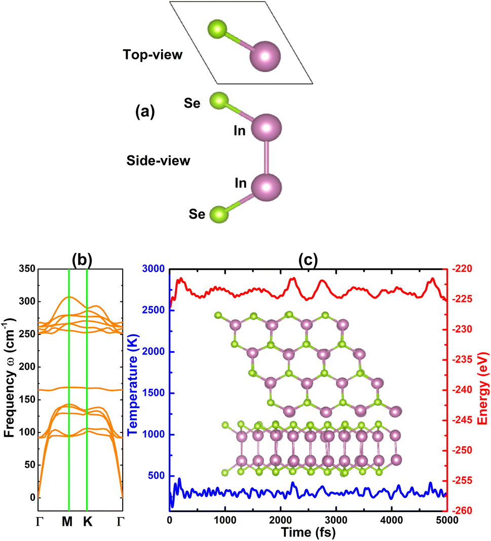 | ||
| Fig. 1 (a) Visualization of a unit cell, (b) phonon dispersion curves, and (c) AIMD simulations at 300 K (final structure + variation of temperature and energy) of the InSe monolayer. | ||
• Cohesive energy Ec of the InSe monolayer is calculated from its unit cell using the following expression:  . A negative Ec value of −3.20 eV indicates good stabilization of the compound state of these 2D materials once formed.
• The dynamic stability of the InSe monolayer is checked through phonon dispersion spectra calculated with the PHONOPY code,46 which is interfaced with density functional perturbation theory (DFPT). From the results plotted in Fig. 1b, no imaginary frequency is found in the whole spectrum, confirming that the InSe monolayer is dynamically stable.
• We then perform ab initio molecular dynamic (AIMD) simulations within the NVT ensemble using the Nose–Hoover method47,48 to verify the thermal stability of the InSe monolayer at 300 K. To prevent the constraints imposed by periodic boundary conditions, a 4 × 4 × 1 supercell is adopted. From the results given in Fig. 1c, one can see stable fluctuation of temperature and energy. Moreover, the monolayer does not undergo remarkable structural distortion after 5000 fs of simulations. These results confirm that the InSe monolayer is thermally stable at room temperature.
According to our results of cohesive energy, phonon calculations, and AIMD simulations, the InSe monolayer has pronounced stability. Furthermore, we proceed to investigate its electronic properties through the band structure and projected density of states (PDOS). Considering the well known band gap underestimation of the GGA-PBE functional, we also calculate the band structure of the pristine InSe monolayer using the hybrid functional HSE06 to get a more accurate band gap.49 From Fig. 2a, it can be concluded that the InSe monolayer is an indirect gap semiconductor as predicted by both employed functionals considering the valence band maximum along the ΓK path and the conduction band minimum at the Γ point. Our PBE- and HSE06-based calculations provide band gap values of 1.41 and 2.16 eV, respectively. PDOS spectra in Fig. 2b assert that the hybridization between In-pz and Se-pz states forms the upper part of the valence band, while the In-s state primarily forms the lower part of conduction band. The electronic hybridization may produce the covalent In–Se chemical bond. However, the difference in electronegativity between the In and Se atoms may also introduce an ionic character through charge transfer. Using Bader charge analysis, it is found that each In atom loses 0.63e of charge that move towards Se atoms.
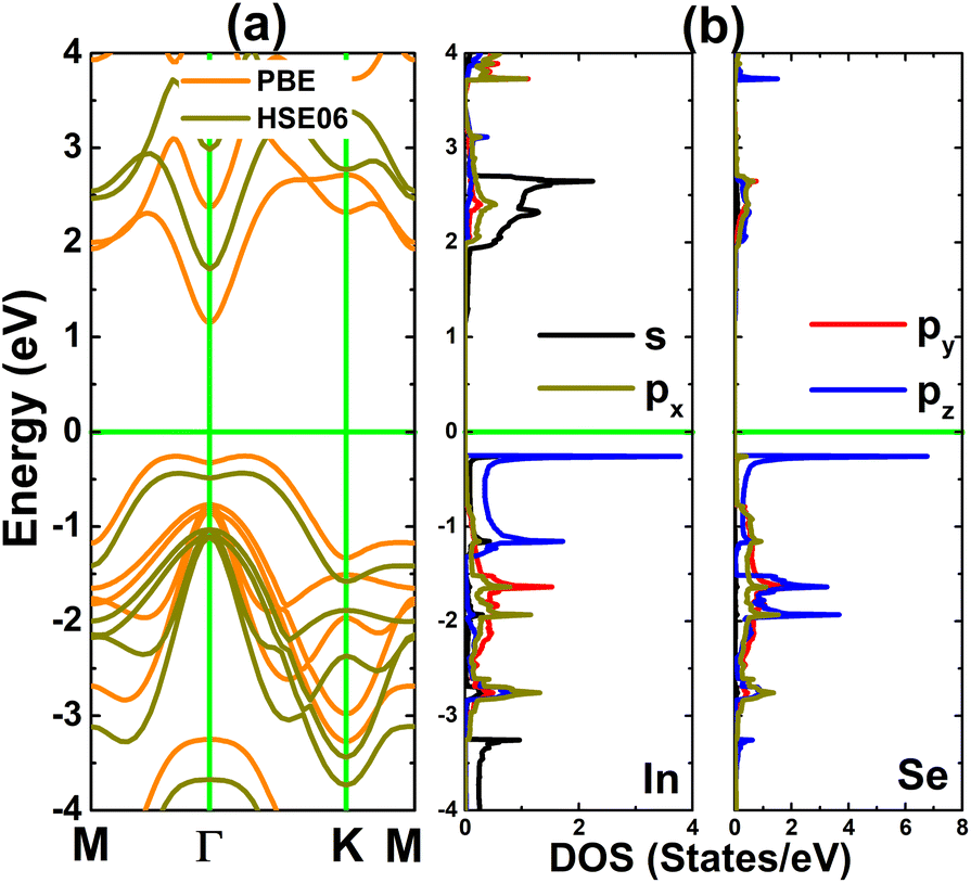 | ||
| Fig. 2 (a) Electronic band structure and (b) projected density of states (calculated with the PBE functional) of the InSe monolayer (horizontal green line: the Fermi level is set to 0 eV). | ||
3.2 Effects of doping at the In sublattice: n-type doping cases
In this part, the effects of doping with IVA- and VA-group atoms at the In sublattice on the InSe monolayer electronic and magnetic properties are investigated. In these cases, two- and one-electron n-type doping is realized, respectively, and we denote the doped systems as XIn@InSe (X = Si, Ge, P, and As). Applying eqn (1), Ef values of 1.41, 1.28, 2.28, and 1.69 eV are obtained for SiIn@InSe, GeIn@InSe, PIn@InSe, and AsIn@InSe systems, respectively. Note that Ge doping requires lower energy than other processes, demonstrating that it is easier to realize. Once formed, all XIn@InSe systems have negative Ec values between −3.21 and −3.18 eV per atom (see Table 1), which are similar to that of the pristine InSe monolayer, asserting their chemical-structural stability.| E f | E c | E g | ΔQ | M t | |
|---|---|---|---|---|---|
| SiIn@InSe | 1.41 | −3.21 | M/M | +1.13 | 0.00 |
| GeIn@InSe | 1.28 | −3.20 | M/M | +0.51 | 0.00 |
| PIn@InSe | 2.28 | −3.18 | 0.76/0.76 | +0.13 | 0.00 |
| AsIn@InSe | 1.69 | −3.18 | 0.93/0.93 | +0.31 | 0.00 |
| SiSe@InSe | 3.01 | −3.18 | 0.83/0.83 | −0.16 | 0.00 |
| GeSe@InSe | 2.46 | −3.17 | 0.83/0.83 | −0.16 | 0.00 |
| PSe@InSe | 1.70 | −3.18 | 1.25/0.43 | −0.58 | 1.00 |
| AsSe@InSe | 1.52 | −3.17 | 1.25/0.39 | −0.46 | 1.00 |
| pSi@InSe | 3.06 | −3.21 | 0.86/0.95 | +0.57/−0.04 | 1.00 |
| pGe@InSe | 2.56 | −3.19 | 0.88/0.68 | +0.28/−0.09 | 1.00 |
| pP@InSe | 2.75 | −3.18 | M/M | 0.00/−0.39 | 0.81 |
| pAs@InSe | 2.32 | −3.17 | 0.62/M | +0.15/−0.31 | 1.00 |
From our spin-polarized calculations, all four XIn@InSe systems have a zero magnetic moment, indicating that n-type doping preserves the nonmagnetic nature of the InSe monolayer. According to Bader charge analysis, Si, Ge, P, and As atoms transfer charge amounts of 1.13, 0.51, 0.13, and 0.31e to the host monolayer, respectively. The absence of magnetism in the doped InSe monolayers is also confirmed by the perfect overlap of spin-up and spin-down orbitals in the band structures displayed in Fig. 3. Importantly, new mid-gap states are induced by Si and Ge doping that extend through the Fermi level, leading to the monolayer metallization. Meanwhile, the results evidence the semiconductor nature of PIn@InSe and AsIn@InSe systems, whose band gaps are considerably smaller than that of the pristine InSe monolayer due to the appearance of mid-gap states. Specifically, these doped systems have energy gaps of 0.76 and 0.93 eV, respectively. Therefore, it can be concluded that n-type doping with P and As atoms leads to a band gap reduction on the order of 46.10% and 34.04% for the InSe monolayer, respectively. The band gap reduction may enhance the potential of the InSe monolayer for optoelectronic applications, widening the working region.
 | ||
| Fig. 3 Spin-polarized band structure of (a) SiIn@InSe, (b) GeIn@InSe, (c) PIn@InSe, and (d) AsIn@InSe monolayer (the Fermi level is set to 0 eV: green horizontal line). | ||
Fig. 4 shows the PDOS spectra of impurities and their first (Se) and second (In) nearest neighboring atoms to further study the origin of monolayer metallization and band gap reduction. In the SiIn@InSe and GeIn@InSe systems, one can see that their metallic nature originates primarily from Si(Ge)-s and In-s states since they overlap with the Fermi level, where a small contribution from the Se-px,y state is also confirmed. Meanwhile, the band gap reduction induced by P and As doping can be attributed to two main factors: (1) P(As)-s, In-pz, and Se-px,y states form mainly the mid-gap states below the Fermi level, and (2) P(As)-px,y and In-s states make a new lower part of the conduction band. Furthermore, spin-up and spin-down states of all orbitals overlap perfectly to evidence again the nonmagnetic nature of XIn@InSe systems.
 | ||
| Fig. 4 Projected density of states of impurities and their nearest neighboring In and Se atoms in (a) SiIn@InSe, (b) GeIn@InSe, (c) PIn@InSe, and (d) AsIn@InSe monolayer (the Fermi level is set to 0 eV: green vertical line). | ||
3.3 Effects of doping at the Se sublattice: p-type doping cases
Herein, we investigate the electronic and magnetic properties of XSe@InSe systems (X = Si, Ge, P, and As), which are formed by doping with X atoms at the Se sublattice to realize p-type doping processes. Applying eqn (2), formation energies of 3.01, 2.46, 1.70, and 1.52 eV are obtained for SiSe@InSe, GeSe@InSe, PSe@InSe, and AsSe@InSe systems, respectively. These results evidence that As doping is easier to achieve, requiring less energy than other processes. It is important to mention that IVA-group impurities may prefer to be doped at the In sublattice rather than the Se sublattice, considering smaller Ef values of SiIn@InSe/GeIn@InSe systems in comparison with SiSe@InSe/GeSe@InSe systems. In contrast, the Se site is the preferred doping site for VA-group impurities as confirmed by the calculated formation energies. Irrespective of the preferred doping site, all the n- and p-doped systems are investigated to clarify role of impurities. Once formed, all four XSe@InSe systems are stabilized as suggested by their negative Ec values between −3.17 and −3.18 eV per atom.Our spin-polarized calculations demonstrate the nonmagnetic nature of SiSe@InSe and GeSe@InSe systems with zero magnetic moments, confirming the preservation of the nonmagnetic nature of the InSe monolayer upon doping with Si and Ge atoms. Meanwhile, doping with VA-group impurities produces an integer total magnetic moment of 1.00 μB in the InSe monolayer. The spin density in PSe@InSe and AsSe@InSe systems is illustrated in Fig. 5. From the figure, one can see that spin surfaces are highly concentrated at P and As sites, respectively. These results evidence that magnetic moments are derived primarily from VA-group dopant atoms. Bader charge analysis is carried out to assert the charge acquisition by impurities when they are incorporated into the Se sublattice. Specifically, Si/Ge, P, and As atoms attract charge amounts of 0.16, 0.58, and 0.46e from the host monolayer, respectively.
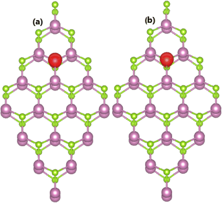 | ||
| Fig. 5 Spin density (Iso-surface value of 0.005 e Å−3) distributed in (a) PSe@InSe and (b) AsSe@InSe systems. | ||
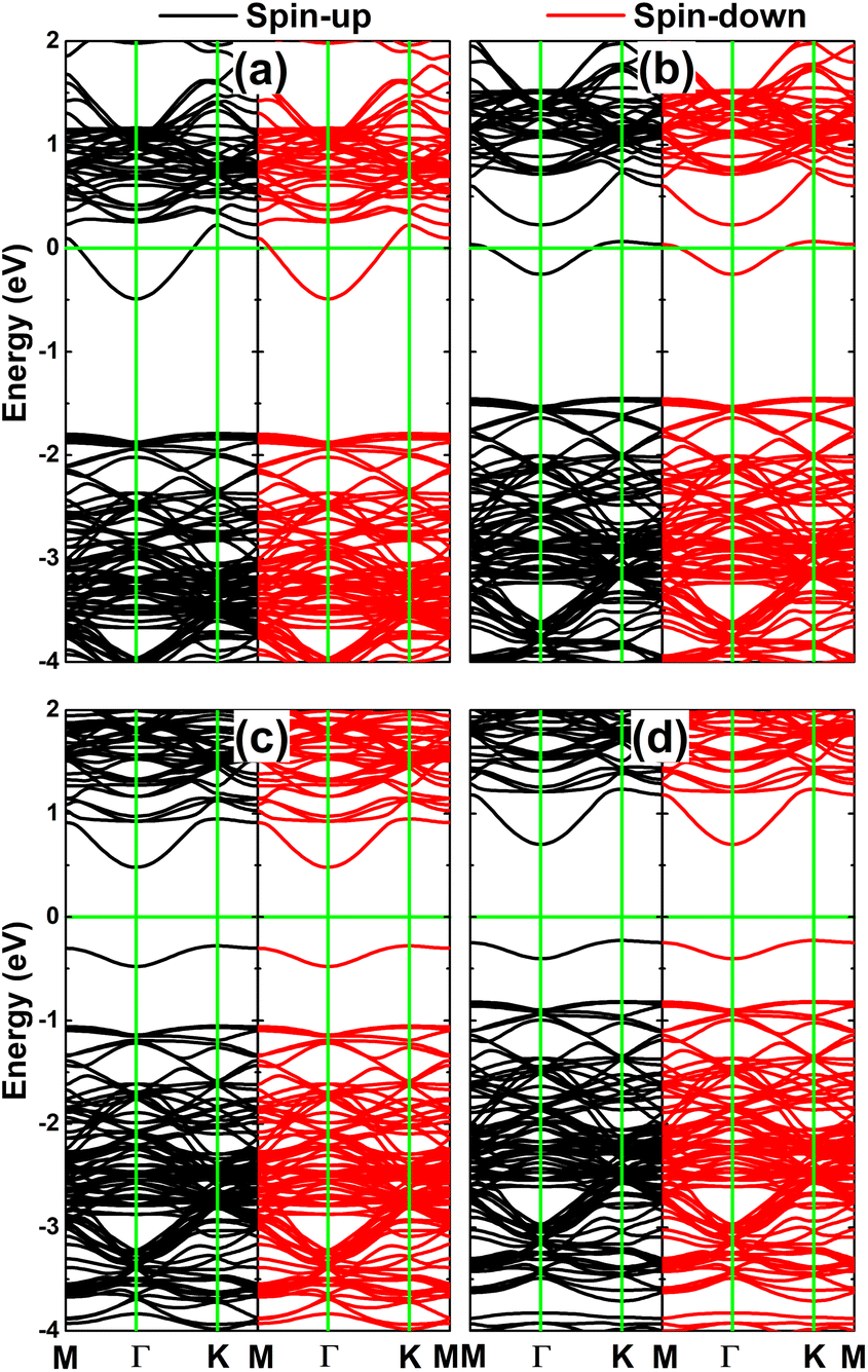
Fig. 6 shows the calculated spin-polarized band structures of XSe@InSe systems. Importantly, a perfect coincidence is observed for SiSe@InSe and GeSe@InSe systems, respectively. In these cases, doping induces a new subband in the upper part of valence band and mid-gap flat energy branches above the Fermi level to reduce the monolayer band gap. Specifically, an energy gap of 0.83 eV is obtained for both systems, which represents a reduction of 41.13% compared to the pristine InSe monolayer. New mid-gap states are also produced by doping with P and As atoms that do not go cross the Fermi level. However they appear at different energy points (one below the spin-up Fermi level and the other above the spin-down Fermi level) resulting in spin polarization in the vicinity of the Fermi level. The band structure profiles evidence the magnetic semiconductor nature of PSe@InSe and AsSe@InSe systems, which may be introduced as prospective spintronic candidates.50 Our calculations provide spin-up/spin-down energy gaps of 1.25/0.43 and 1.25/0.39 eV for PSe@InSe and AsSe@InSe systems, respectively.
 | ||
| Fig. 6 Spin-polarized band structure of (a) SiSe@InSe, (b) GeSe@InSe, (c) PSe@InSe, and (d) AsSe@InSe monolayer (the Fermi level is set to 0 eV: green horizontal line). | ||
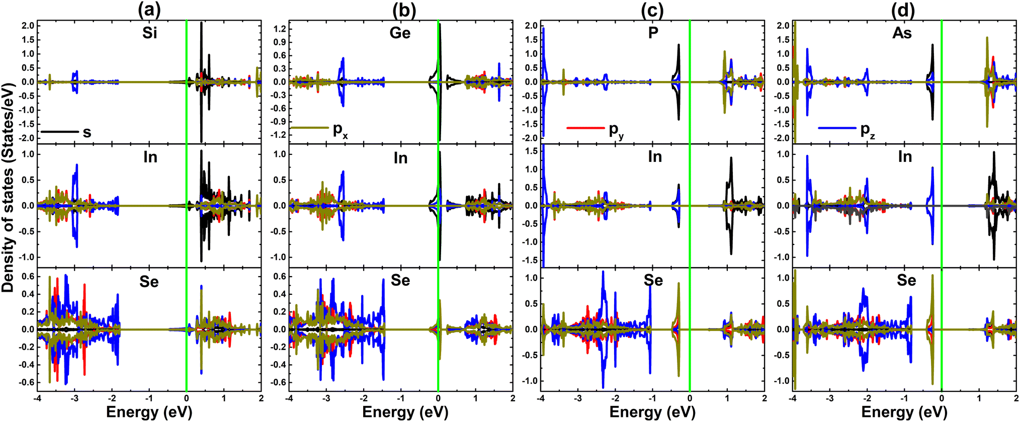
PDOS spectra of impurities and their first (In) nearest neighboring atoms are given in Fig. 7 to further study the electronic structure and physical origin of magnetism. When doping with IVA-group atoms, X-px,y states hybridize with In-px,y,z states to form a subband in the upper part of the valence band, while the flat branches above the Fermi level primarily originate from X-pz states. Meanwhile, the magnetic semiconductor nature of the PSe@InSe and AsSe@InSe systems is mainly due to the pz state of impurities since it generates mainly the flat energy states around the Fermi level, where a small contribution from In-px,y,z states is also noted. The PDOS profile also evidences the important role of P-pz and As-pz states in producing the magnetism of PSe@InSe and AsSe@InSe systems, respectively.
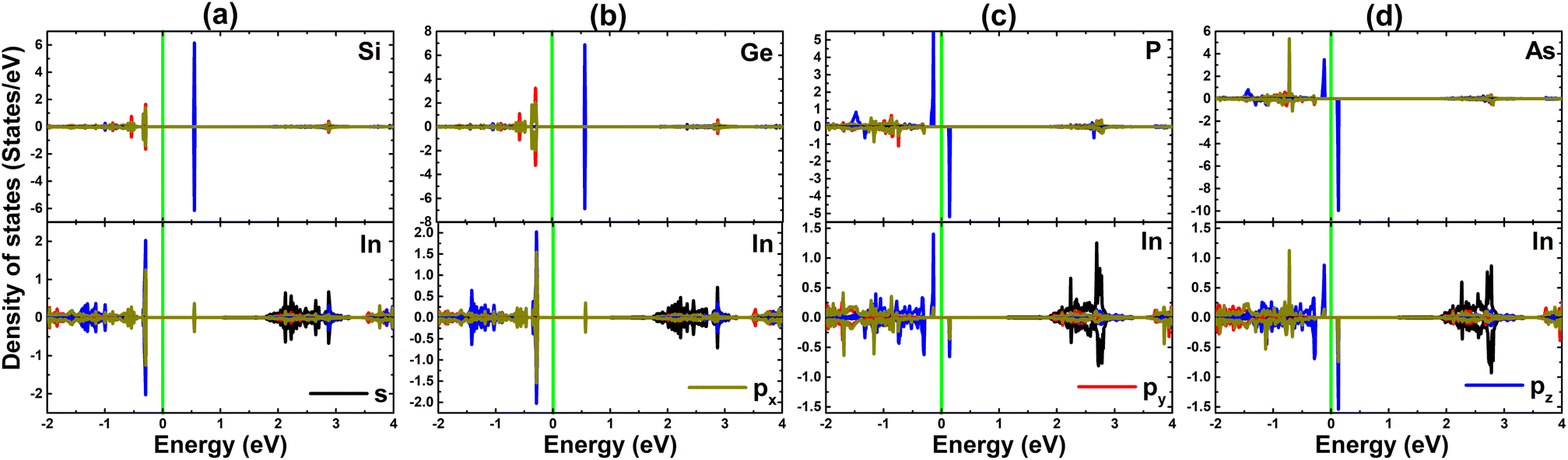 | ||
| Fig. 7 Projected density of states of impurities and their nearest neighboring In atoms in (a) SiSe@InSe, (b) GeSe@InSe, (c) PSe@InSe, and (d) AsSe@InSe monolayer (the Fermi level is set to 0 eV: green vertical line). | ||
3.4 Effects of simultaneous doping at In + Se sublattices
Now, doping with pair dopant atoms is proposed to modify the InSe monolayer electronic and magnetic properties. The doped systems are named pX@InSe (X = Si, Ge, P, and As), where X1 and X2 refer to impurity incorporated at the In sublattice and Se sublattice, respectively. Applying eqn (3), Ef values of 3.06, 2.56, 2.75, and 2.32 eV are obtained for pSi@InSe, pGe@InSe, pP@InSe, and pAs@InSe systems, respectively. The results indicate that doping with As–As pairs is energetically most favorable and easier to realize as compared with other cases. The calculated (negative-feature) cohesive energies (see Table 1) suggest good structural and chemical stability of all four pX@InSe systems once they have been formed.It is found that the InSe monolayer is magnetized by doping with pair IVA- and VA-group atoms, as confirmed by the nonzero magnetic moments. Specifically, integer total magnetic moments of 1.00 μB are obtained for pSi@InSe, pGe@InSe, and pAs@InSe systems, while a smaller value of 0.81 μB is obtained for the pP@InSe system. Fig. 8 visualizes the spin density in pX@InSe systems, where different features are observed depending on the nature of impurities. A high concentration of spin surfaces indicates that magnetic moments of pSi@InSe and pGe@InSe systems are produced primarily by Si2 and Ge2 dopant atoms. Meanwhile, P1 and As1 impurities produce mainly the magnetic moments of pP@InSe and pAs@InSe systems, respectively, with a small contribution from their first nearest neighboring Se atoms. Furthermore, Bader charge analysis indicates that X1 impurities act as charge donors, while X2 dopant atoms are confirmed to act as charge acceptors. The calculated charge quantities are listed in Table 1.
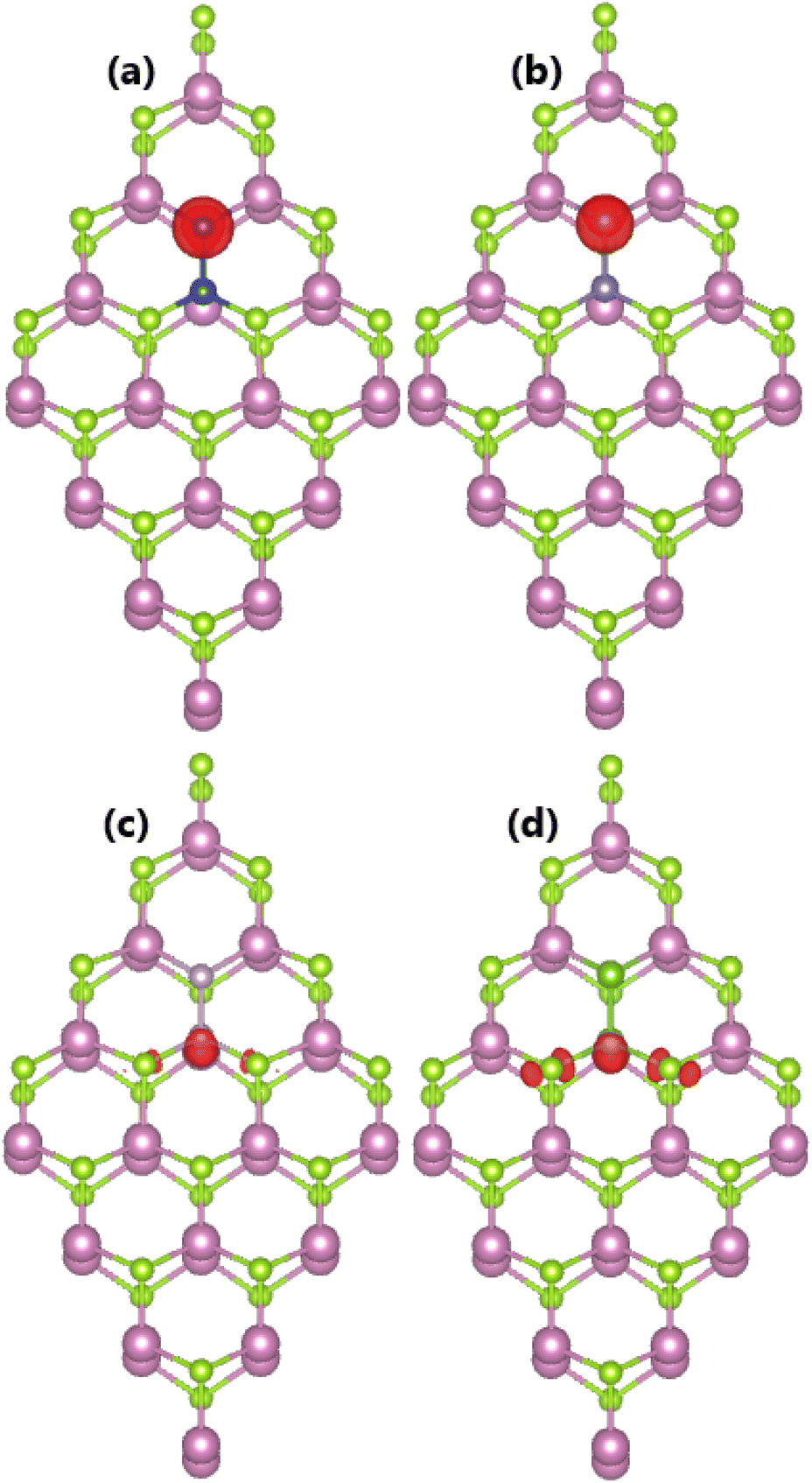 | ||
| Fig. 8 Spin density (Iso-surface value of 0.005 e Å−3) distributed in (a) pSi@InSe, (b) pGe@InSe, (c) pP@InSe, and (d) pAs@InSe systems. | ||
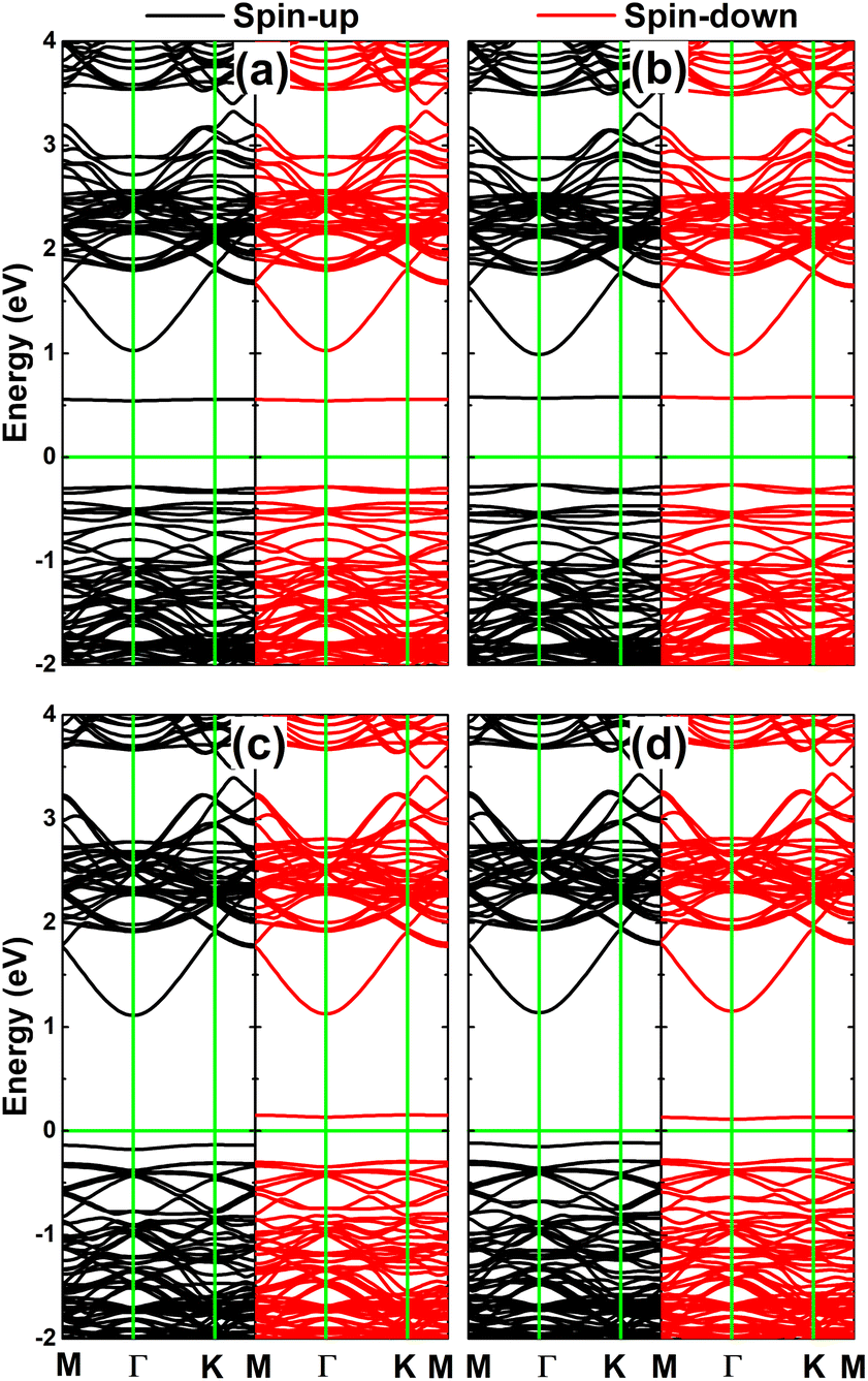
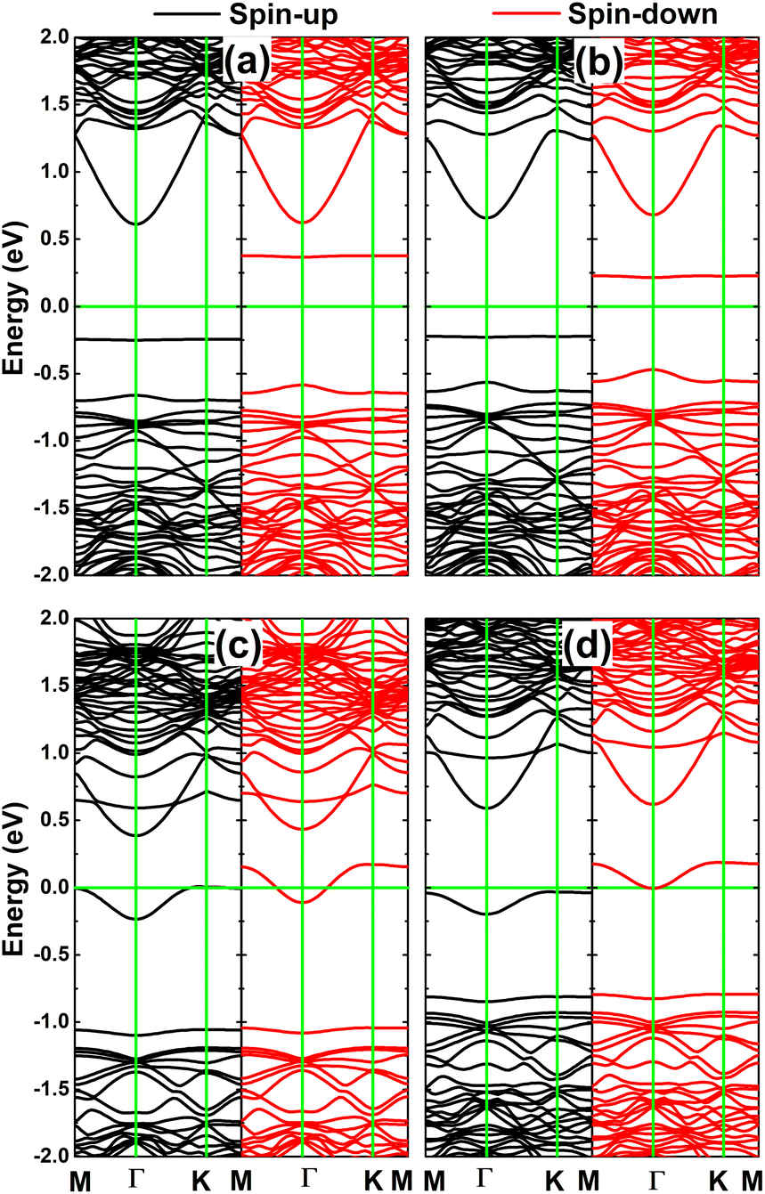
Fig. 9 shows the calculated spin-polarized band structures of the InSe monolayer engineered by doping with pair atoms. In all cases, the spin-up and spin-down channels around the Fermi level show strong splitting with the appearance of new mid-gap energy branches, further reflecting the engineered magnetism. pSi@InSe and pGe@InSe are confirmed to be magnetic semiconductor systems since no energy branch overlaps with the Fermi level. In these cases, spin-up/spin-down states have energy gaps of 0.86/0.95 and 0.88/0.68 eV, respectively. In contrast, both spin states of the pP@InSe monolayer exhibit metallic character, confirming the monolayer metallization induced by doping with pair P atoms. On the other hand, metallic character is only observed for the spin-down state of the pAs@InSe monolayer, while the semiconductor spin-up state with an energy gap of 0.62 eV is obtained. These results evidence the half-metallicity of the pAs@InSe monolayer that is another desirable feature for spintronic applications.51
 | ||
| Fig. 9 Spin-polarized band structure of (a) pSi@InSe, (b) pGe@InSe, (c) pP@InSe, and (d) pAs@InSe systems (the Fermi level is set to 0 eV: green horizontal line). | ||
To further study the contribution of IVA- and VA-group impurities, the total density of states and their atom-decomposed density of states are given in Fig. 10. Focusing on the region around the Fermi level, it is noted that Si2 and Ge2 atoms mainly contribute to the mid-gap states of pSi@InSe and pAs@InSe systems, respectively. Meanwhile, in pP@InSe and pAs@InSe systems, the mid-gap states are formed primarily by the P1 and As1 dopant atoms to regulate the electronic nature of the systems, respectively. Strong spin splitting also confirms the role of Si2, Ge2, P1, and As1 in producing magnetism in respective pair-atoms-doped systems. Therefore, it can be concluded that the band structure and magnetism are engineered mainly by the mentioned impurities.
 | ||
| Fig. 10 Total density of states and atomic density of states of impurities of (a) pSi@InSe, (b) pGe@InSe, (c) pP@InSe, and (d) pAs@InSe systems (the Fermi level is set to 0 eV: Green vertical line). | ||
4. Conclusions
Using the spin-polarized DFT calculations, we developed a complete first-principles framework to investigate the feature-rich properties of IVA and VA group atom-doped InSe monolayers, including electronic band structures, projected density of states, and spin density distributions. The pristine InSe monolayer possesses good structural, dynamical, and thermal stability, exhibiting an indirect-gap semiconductor nature. Atom substitution generates new mid-gap energy states that determine the electronic and magnetic properties of the doped InSe monolayers. No magnetism is induced by n-type doping, where one electron doping metallizes the monolayer and two electron doping decreases significantly the monolayer's band gap. In these cases, the s states of impurities primarily contribute to formation of mid-gap states. Regarding the p-type doping process, two-hole doping results in a band gap reduction without magnetism, while one hole doping leads to a magnetic semiconductor nature with a total magnetic moment of 1.00 μB. Herein, the modification can be attributed mainly to the pz state of the dopant atoms when forming mainly the band structure around the Fermi level. Interestingly, the substitution of pair IVA-group atoms makes new magnetic semiconductor materials with a total magnetic moment of 1.00 μB despite no magnetism being induced by a single impurity. The electronic and magnetic properties of the pSi@InSe and pGe@InSe systems are regulated primarily by the dopant atoms incorporated at the Se site. Meanwhile, impurities incorporated at In site determine the ground-state properties of pP@InSe and pAs@InSe systems that are confirmed to be magnetic metallic and half-metallic materials, respectively. Our study provides insights into the effects of doping sites on the electronic and magnetic properties of doped InSe monolayers, which can be used as valuable guidance to realize the functionalization of this 2D material towards multifunctional applications.Data availability
Data related to this study are available upon reasonable request.Conflicts of interest
The authors declare that they have no known competing financial interests or personal relationships that could have appeared to influence the work reported in this paper.Acknowledgements
The calculations were performed at the DGCTIC-UNAM Supercomputing Center (projects LANCAD-UNAM-DGTIC-368).References
- J. Shim, H.-Y. Park, D.-H. Kang, J.-O. Kim, S.-H. Jo, Y. Park and J.-H. Park, Electronic and optoelectronic devices based on two-dimensional materials: From fabrication to application, Adv. Electron. Mater., 2017, 3(4), 1600364 CrossRef.
- S. Kang, D. Lee, J. Kim, A. Capasso, H. S. Kang, J.-W. Park, C.-H. Lee and G.-H. Lee, 2D semiconducting materials for electronic and optoelectronic applications: potential and challenge, 2D Materials, 2020, 7(2), 022003 CrossRef CAS.
- M. Turunen, M. Brotons-Gisbert, Y. Dai, Y. Wang, E. Scerri, C. Bonato, K. D. Jöns, Z. Sun and B. D. Gerardot, Quantum photonics with layered 2D materials, Nat. Rev. Phys., 2022, 4(4), 219–236 CrossRef.
- F. Xia, H. Wang, D. Xiao, M. Dubey and A. Ramasubramaniam, Two-dimensional material nanophotonics, Nat. Photonics, 2014, 8(12), 899–907 CrossRef CAS.
- D. Deng, K. Novoselov, Q. Fu, N. Zheng, Z. Tian and X. Bao, Catalysis with two-dimensional materials and their heterostructures, Nat. Nanotechnol., 2016, 11(3), 218–230 CrossRef CAS PubMed.
- H. Li, J. Xiao, Q. Fu and X. Bao, Confined catalysis under two-dimensional materials, Proc. Natl. Acad. Sci. U. S. A., 2017, 114(23), 5930–5934 CrossRef CAS.
- X. Liu, T. Ma, N. Pinna and J. Zhang, Two-dimensional nanostructured materials for gas sensing, Adv. Funct. Mater., 2017, 27(37), 1702168 Search PubMed.
- M. Mathew, P. V. Shinde, R. Samal and C. S. Rout, A review on mechanisms and recent developments in pn heterojunctions of 2D materials for gas sensing applications, J. Mater. Sci., 2021, 56, 9575–9604 CrossRef CAS.
- D. Chimene, D. L. Alge and A. K. Gaharwar, Two-dimensional nanomaterials for biomedical applications: emerging trends and future prospects, Adv. Mater., 2015, 27(45), 7261–7284 CrossRef CAS PubMed.
- T. Hu, X. Mei, Y. Wang, X. Weng, R. Liang and M. Wei, Two-dimensional nanomaterials: fascinating materials in biomedical field, Sci. Bull., 2019, 64(22), 1707–1727 CrossRef CAS.
- Y. Xue, Q. Zhang, W. Wang, H. Cao, Q. Yang and L. Fu, Opening two-dimensional materials for energy conversion and storage: a concept, Adv. Energy Mater., 2017, 7(19), 1602684 CrossRef.
- X. Zhang, L. Hou, A. Ciesielski and P. Samorì, 2D materials beyond graphene for high-performance energy storage applications, Adv. Energy Mater., 2016, 6(23), 1600671 CrossRef.
- K. Rasool, R. P. Pandey, P. A. Rasheed, S. Buczek, Y. Gogotsi and K. A. Mahmoud, Water treatment and environmental remediation applications of two-dimensional metal carbides (MXenes), Mater. Today, 2019, 30, 80–102 CrossRef CAS.
- T.-H. Le, Y. Oh, H. Kim and H. Yoon, Exfoliation of 2D materials for energy and environmental applications, Chem.–Eur. J., 2020, 26(29), 6360–6401 CrossRef CAS.
- K. S. Novoselov, A. K. Geim, S. V. Morozov, D.-e. Jiang, Y. Zhang, S. V. Dubonos, I. V. Grigorieva and A. A. Firsov, Electric field effect in atomically thin carbon films, science, 2004, 306(5696), 666–669 CrossRef CAS.
- C. Soldano, A. Mahmood and E. Dujardin, Production, properties and potential of graphene, Carbon, 2010, 48(8), 2127–2150 CrossRef CAS.
- M. J. Allen, V. C. Tung and R. B. Kaner, Honeycomb carbon: a review of graphene, Chem. Rev., 2010, 110(1), 132–145 CrossRef CAS PubMed.
- Y.-W. Son, M. L. Cohen and S. G. Louie, Energy gaps in graphene nanoribbons, Phys. Rev. Lett., 2006, 97(21), 216803 CrossRef.
- J. E. Johns and M. C. Hersam, Atomic covalent functionalization of graphene, Acc. Chem. Res., 2013, 46(1), 77–86 CrossRef CAS.
- M. Chhowalla, Z. Liu and H. Zhang, Two-dimensional transition metal dichalcogenide (TMD) nanosheets, Chem. Soc. Rev., 2015, 44(9), 2584–2586 RSC.
- X. Duan, C. Wang, A. Pan, R. Yu and X. Duan, Two-dimensional transition metal dichalcogenides as atomically thin semiconductors: opportunities and challenges, Chem. Soc. Rev., 2015, 44(24), 8859–8876 RSC.
- Y. Wei, P. Zhang, R. A. Soomro, Q. Zhu and B. Xu, Advances in the synthesis of 2D MXenes, Adv. Mater., 2021, 33(39), 2103148 CrossRef CAS.
- D. Ayodhya, A review of recent progress in 2D MXenes: Synthesis, properties, and applications, Diamond Relat. Mater., 2023, 132, 109634 CrossRef CAS.
- K. Khan, A. K. Tareen, Q. U. Khan, M. Iqbal, H. Zhang and Z. Guo, Novel synthesis, properties and applications of emerging group VA two-dimensional monoelemental materials (2D-Xenes), Mater. Chem. Front., 2021, 5(17), 6333–6391 Search PubMed.
- H. Şahin, S. Cahangirov, M. Topsakal, E. Bekaroglu, E. Akturk, R. T. Senger and S. Ciraci, Monolayer honeycomb structures of group-iv elements and iii-v binary compounds: First-principles calculations, Phys. Rev. B:Condens. Matter Mater. Phys., 2009, 80(15), 155453 CrossRef.
- F. Ersan, D. Keçik, V. Özçelik, Y. Kadioglu, O. Ü. Aktürk, E. Durgun, E. Aktürk and S. Ciraci, Two-dimensional pnictogens: A review of recent progresses and future research directions, Applied Physics Reviews, 2019, 6(2), 021308 CrossRef.
- C. V. Ha, L. Ha, D. K. Nguyen, D. T. Anh, J. Guerrero-Sanchez and D. Hoat, et al., First-principles study of SiC and GeC monolayers with adsorbed non-metal atoms, RSC Adv., 2023, 13(22), 14879–14886 RSC.
- H. L. Zhuang, A. K. Singh and R. G. Hennig, Computational discovery of single-layer III-V materials, Phys. Rev. B:Condens. Matter Mater. Phys., 2013, 87(16), 165415 CrossRef.
- X.-F. Liu, Z.-J. Luo, X. Zhou, J.-M. Wei, Y. Wang, X. Guo, B. Lv and Z. Ding, Structural, mechanical, and electronic properties of 25 kinds of III–V binary monolayers: A computational study with first-principles calculation, Chin. Phys. B, 2019, 28(8), 086105 CrossRef CAS.
- H. Wang, G. Qin, J. Yang, Z. Qin, Y. Yao, Q. Wang and M. Hu, First-principles study of electronic, optical and thermal transport properties of group III–VI monolayer MX (M= Ga, In; X= S, Se), J. Appl. Phys., 2019, 125(24), 245104 CrossRef.
- S. Demirci, N. Avazlı, E. Durgun and S. Cahangirov, Structural and electronic properties of monolayer group III monochalcogenides, Phys. Rev. B, 2017, 95(11), 115409 CrossRef.
- J. Chen, X. Tan, P. Lin, B. Sa, J. Zhou, Y. Zhang, C. Wen and Z. Sun, Comprehensive understanding of intrinsic mobility in the monolayers of III–VI group 2D materials, Phys. Chem. Chem. Phys., 2019, 21(39), 21898–21907 RSC.
- G. W. Mudd, S. A. Svatek, T. Ren, A. Patanè, O. Makarovsky, L. Eaves, P. H. Beton, Z. D. Kovalyuk, G. V. Lashkarev and Z. R. Kudrynskyi, et al., Tuning the bandgap of exfoliated InSe nanosheets by quantum confinement, Adv. Mater., 2013, 25(40), 5714 CrossRef CAS PubMed.
- E. Petroni, E. Lago, S. Bellani, D. W. Boukhvalov, A. Politano, B. Gürbulak, S. Duman, M. Prato, S. Gentiluomo and R. Oropesa-Nuñez, et al., Liquid-phase exfoliated indium–selenide flakes and their application in hydrogen evolution reaction, Small, 2018, 14(26), 1800749 CrossRef.
- H.-C. Chang, C.-L. Tu, K.-I. Lin, J. Pu, T. Takenobu, C.-N. Hsiao and C.-H. Chen, Synthesis of large-area InSe monolayers by chemical vapor deposition, Small, 2018, 14(39), 1802351 CrossRef PubMed.
- J. Zhou, J. Shi, Q. Zeng, Y. Chen, L. Niu, F. Liu, T. Yu, K. Suenaga, X. Liu and J. Lin, et al., InSe monolayer: synthesis, structure and ultra-high second-harmonic generation, 2D Materials, 2018, 5(2), 025019 CrossRef.
- C. Zhang, X. Chen, B. Cao, H. Duan, Q. Sun and F. Ouyang, Tuning the band gap of the InSe monolayer by substitutional doping, Appl. Surf. Sci., 2022, 579, 152190 CrossRef CAS.
- W. Ju, T. Li, Q. Zhou, H. Li, X. Li and D. Ma, Adsorption of 3d transition-metal atom on InSe monolayer: a first-principles study, Comput. Mater. Sci., 2018, 150, 33–41 CrossRef CAS.
- V.-T. Pham and T.-H. Fang, Effects of temperature and intrinsic structural defects on mechanical properties and thermal conductivities of InSe monolayers, Sci. Rep., 2020, 10(1), 15082 CrossRef CAS PubMed.
- W. Kohn and L. J. Sham, Self-consistent equations including exchange and correlation effects, Phys. Rev., 1965, 140(4A), A1133 CrossRef.
- G. Kresse and J. Furthmüller, Efficiency of ab initio total energy calculations for metals and semiconductors using a plane-wave basis set, Comput. Mater. Sci., 1996, 6(1), 15–50 CrossRef CAS.
- G. Kresse and J. Furthmüller, Efficient iterative schemes for ab initio total-energy calculations using a plane-wave basis set, Phys. Rev. B:Condens. Matter Mater. Phys., 1996, 54(16), 11169 Search PubMed.
- J. P. Perdew, K. Burke and M. Ernzerhof, Generalized gradient approximation made simple, Phys. Rev. Lett., 1996, 77(18), 3865 CrossRef CAS.
- T. M. Project, Materials data on InSe by materials project, DOI:10.17188/1195613.
- H. J. Monkhorst and J. D. Pack, Special points for Brillouin-zone integrations, Phys. Rev. B:Condens. Matter Mater. Phys., 1976, 13(12), 5188 CrossRef.
- A. Togo, L. Chaput, T. Tadano and I. Tanaka, Implementation strategies in phonopy and phono3py, J. Phys.:Condens. Matter, 2023, 35(35), 353001, DOI:10.1088/1361-648X/acd831.
- S. Nosé, A unified formulation of the constant temperature molecular dynamics methods, J. Chem. Phys., 1984, 81(1), 511–519 CrossRef.
- W. G. Hoover, Canonical dynamics: Equilibrium phase-space distributions, Phys. Rev. A:At., Mol., Opt. Phys., 1985, 31(3), 1695 CrossRef.
- A. V. Krukau, O. A. Vydrov, A. F. Izmaylov and G. E. Scuseria, Influence of the exchange screening parameter on the performance of screened hybrid functionals, J. Chem. Phys., 2006, 125(22), 224106 CrossRef.
- X. Li and J. Yang, First-principles design of spintronics materials, Natl. Sci. Rev., 2016, 3(3), 365–381 CrossRef CAS.
- X. Li and J. Yang, Low-dimensional half-metallic materials: theoretical simulations and design, Wiley Interdiscip. Rev.: Comput. Mol. Sci., 2017, 7(4), e1314 Search PubMed.
| This journal is © The Royal Society of Chemistry 2025 |