
 Open Access Article
 This Open Access Article is licensed under a Creative Commons Attribution-Non Commercial 3.0 Unported Licence
Atomic layer deposition of Ru in nanoTSV with high coverage and low resistivity
Zhao Chen ab,
Feifeng Huangab,
Biao Wangab,
Qiancheng Wangab,
Hongbin Chenab,
Qiu Shaoab,
Bo Feng*ab,
Ming Jic and
Huigao Duanab
ab,
Feifeng Huangab,
Biao Wangab,
Qiancheng Wangab,
Hongbin Chenab,
Qiu Shaoab,
Bo Feng*ab,
Ming Jic and
Huigao Duanab
aCollege of Mechanical and Vehicle Engineering, Hunan University, Changsha 410082, People's Republic of China. E-mail: fengbo36@hnu.edu.cn
bGreater Bay Area Institute for Innovation, Hunan University, Guangzhou 511300, People's Republic of China
cIBD Technology Co., Ltd, Zhongshan, Guangdong Province, China
First published on 1st May 2025
Abstract
With the advancement of Moore's Law, the metal linewidth has gradually reduced and Cu interconnection has lost its advantages. This paper explores the advantage of ruthenium (Ru) as a next-generation interconnection material. An Ru film with a resistivity of 15 μΩ cm and roughness of 0.8 nm was fabricated via atomic layer deposition (ALD) using the metal–organic precursor (bis(ethylcyclopentadienyl)ruthenium [Ru(EtCp)2]) and oxygen as the reactant. Excellent step coverage and filling in nanoTSV arrays with a critical dimension (CD) of 30 nm and an aspect ratio (AR) of approximately 15 demonstrate that the reported process is highly promising for fabricating Ru as a replacement for Cu interconnects in advanced integrated circuits (ICs).
1. Introduction
Since the early 2000s, Cu has been the most commonly used interconnect material for ICs owing to its low resistivity and superior reliability.1 With the continuous development of IC technology, the dimensions of metal interconnects are progressively reducing, leading to a significant increase in Cu resistance, attributed to the electron surface scattering effect.2–5 The increase in resistance will lead to considerable interconnect delay. The high delay will significantly affect signal transmission speed and thereby reduce the overall computing speed of the IC.6,7 To solve this problem, it is of great significance to find the next generation of interconnect materials that can replace Cu.Owing to its good chemical stability, thermal stability, excellent electrical properties, low resistivity (approximately 7.1 μΩ cm), high work function (approximately 4.7 eV), and its ability for dry etching, Ru films have found many applications in the field of microelectronics, such as in gate materials as a substitute for W and in capacitor electrodes in dynamic random access memory (DRAM).8–12 More interestingly, Ru is considered one of the most promising metals that can replace Cu interconnects.4,13–16
Atomic layer deposition (ALD) is a thin film preparation technique that allows layer-by-layer growth at the atomic level with precise thickness control and high coverage. ALD can be used to grow thin films on nanostructured substrates for a variety of applications, including nanoelectronic devices.17,18 It has been reported that many researchers have explored the growth of Ru films on the planar substrates using ALD.19–25 Ru films have been grown via ALD using various precursors, including [Ru(chd)2],26 [Ru(Cp)2],27 [Ru(DMBD)(CO)3],28 and [Ru(EtCp)2].29–36 These films have shown excellent performance, such as low resistivity (15–20 μΩ cm). However, there is still a lack of reliable processes for filling Ru in high-aspect-ratio and extremely narrow trenches. The most significant limitation of this process is that there will be some voids in the trenches, and it is challenging to obtain void-free filling in high-aspect-ratio trenches.
In this paper, Ru(EtCp)2 was selected as the precursor owing to its high saturated vapor pressure, and the resultant Ru films exhibited low resistivity. We successfully developed the process through ALD using Ru(EtCp)2 and oxygen gas to fabricate Ru films with low resistivity, low roughness, and a high growth rate. Then, we developed an Ru-filled nanoTSV (through-silicon via) process to examine the damascene process of Ru. Interestingly, Ru was successfully filled into nanoTSV with high coverage and low resistivity through ALD.
2. Experimental
Ru films were deposited on SiO2 (10 nm-thick)/Si wafers using an ALD reactor (NCE200R) with an 8-inch diameter wafer scale. SiO2 films were prepared via ALD. A metal–organic precursor (bis(ethylcyclopentadienyl)ruthenium [Ru(EtCp)2]) and oxygen gas were used as the ruthenium precursor and reactant, respectively. The reaction principle is shown in Fig. 1. The deposition temperature and pressure during ALD were 260–310 °C and 1 torr, respectively. Ru(EtCp)2 is a yellow liquid precursor at room temperature with good thermal stability and a relatively high vapor pressure of 0.18 torr at 80 °C. The Ru precursor was vaporized in a bubbler at 80 °C and carried to the process chamber using argon with a flow rate of 120 sccm. The temperature of the precursor conveying system was maintained at 125 °C to prevent precursor condensation. One deposition cycle for Ru films comprised four steps: a Ru(EtCp)2 vapor pulse, a purge pulse with 120 sccm argon gas, a pulse for exposure to oxygen gas, and another purge pulse with 120 sccm argon gas. This cycle can be repeated several times to obtain the desired film thickness.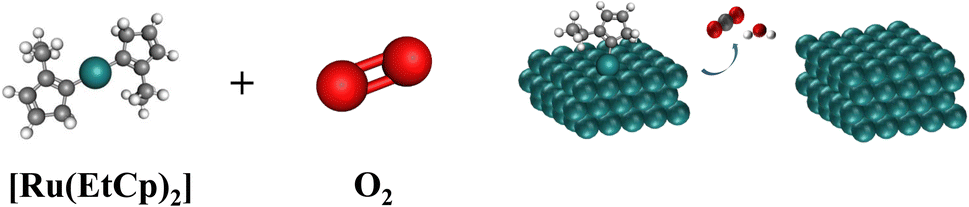 | ||
| Fig. 1 Reaction principle of atomic layer deposition. | ||
The thickness of Ru films was measured using field-emission scanning electron microscopy (FESEM) and transmission electron microscopy (TEM). Film resistivity was calculated from the film thickness and sheet resistance measured using a four-point probe. Film composition and impurity were analysed using X-ray photoelectron spectroscopy (XPS, Nexsa G2 Thermo Fisher). The film surface was observed using FESEM, and the roughness of films was measured using atomic force microscopy (AFM, SPA-300, Seiko).
3. Results and discussion
First, to evaluate the effect of the Ru(EtCp)2 pulse time, the dependence of the deposited Ru film growth per cycle (GPC) and the resistivity were investigated. The deposition temperature and pressure during ALD were 300 °C and 1 torr, respectively. The pulse time of oxygen gas was fixed at 12 s. The number of ALD deposition cycles was 750. As shown in Fig. 2a, as the Ru(EtCp)2 pulse time increased, the deposited Ru film GPC gradually increased. Interestingly, when the pulse time exceeded 3 s, the growth rate did not increase and remained at 0.6 Å per cycle. This indicates that the film deposition follows one of the inherent characteristics of ALD, a so-called self-limited reaction.32 Moreover, as the Ru(EtCp)2 pulse time increased, the resistivity of the deposited Ru film sharply decreased from 45 μΩ cm to a stable value of approximately 15 μΩ cm. This unusual phenomenon attracted our attention.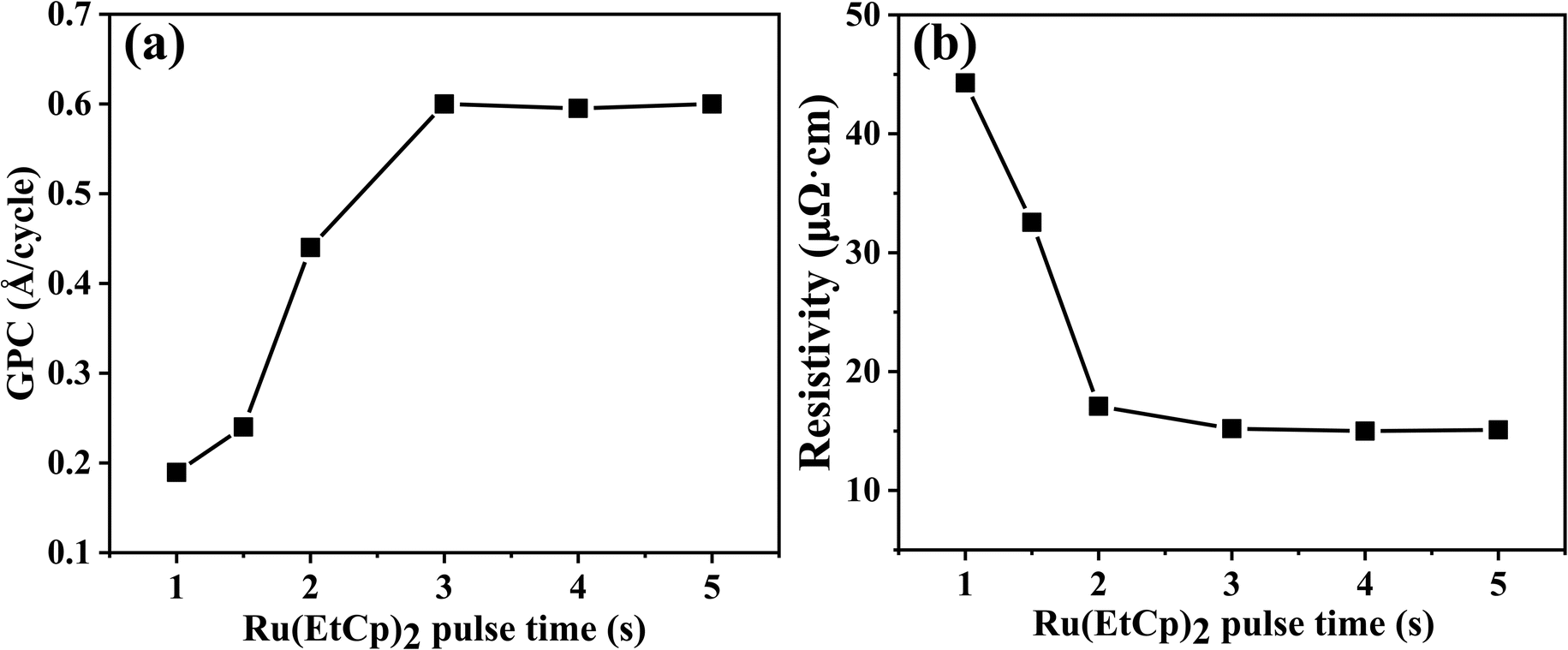 | ||
| Fig. 2 ALD Ru films deposited on SiO2/Si substrates at 300 °C as a function of Ru(EtCp)2 pulse time. The pulse time of O2 was fixed to 12 s and the number of ALD deposition cycles was 750: (a) the dependence of GPC on Ru(EtCp)2 pulse time. (b) The dependence of resistivity on Ru(EtCp)2 pulse time. | ||
To investigate this unusual phenomenon for Ru film deposition, XPS analyses were performed on Ru films deposited at 300 °C with Ru(EtCp)2 pulse times of 1 and 3 s, respectively. As can be seen in Fig. 3, when the Ru(EtCp)2 pulse time was 1 s, three distinct peaks were observed in the XPS spectra. The Ru 3d doublets can be attributed to spin–orbit splitting, resulting in distinct binding energy peaks for the Ru 3d5/2 and 3d3/2 orbitals. The peaks at 280.1 and 284.3 eV correspond to the Ru 3d5/2 and 3d3/2 states of metallic Ru, respectively, while the peak at 280.7 eV can be attributed to RuO2. When the Ru(EtCp)2 pulse time was 3 s, the XPS spectra only showed the peaks of Ru 3d5/2 and 3d3/2 without any signal corresponding to RuO2. This indicated that when the pulse time of Ru(EtCp)2 was less than 3 s, the reaction between Ru(EtCp)2 and O2 did not result in the formation of pure Ru. Instead, a side-reaction took place, leading to the formation of RuO2. This finding was consistent with a previous study that investigated the influence of Ru(EtCp)2 pulse time on the properties of ALD Ru films.32 The resistivity of RuO2 (approximately 70 μΩ cm) is considerably higher than that of metallic Ru (approximately 15 μΩ cm), suggesting that the presence of RuO2 impurities is an important factor contributing to the elevated resistivity of Ru films deposited under insufficient precursor pulse conditions. When the Ru(EtCp)2 pulse time was greater than or equal to 3 s, the resistivity stabilized at approximately 15 μΩ cm, demonstrating the successful deposition of oxygen-free metallic Ru. This indicates that for certain reaction temperature and oxygen, the amount of Ru precursor will determine whether RuO2 is produced.
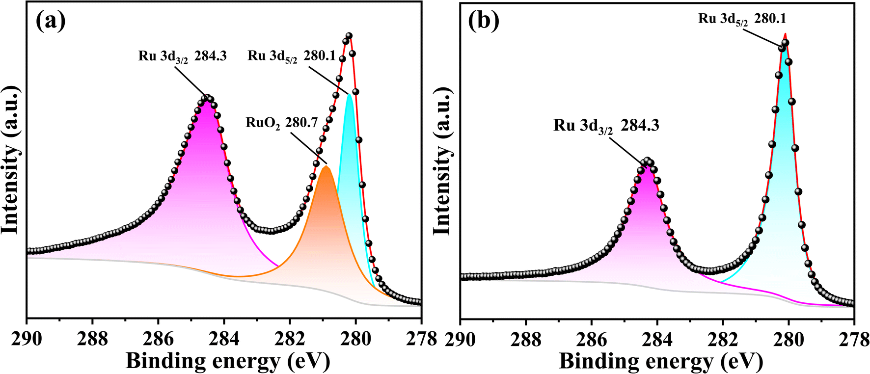 | ||
| Fig. 3 XPS of ALD Ru films deposited on SiO2/Si substrates at temperatures of 300 °C: (a) the Ru(EtCp)2 pulse time for 1 s. (b) The Ru(EtCp)2 pulse time for 3 s. | ||
Subsequently, the nanoTSV arrays were filled at 300 °C with the pulse times of Ru(EtCp)2 and O2 being set to 3 and 12 s, respectively. As can be seen in Fig. 4a, the nanoTSV arrays were not perfectly filled. There were voids in the middle of the trenches that were not densely filled, which could be seen from the elemental analysis in Fig. 4b. The grain size of Ru was relatively large. The roughness of the Ru film was analysed by AFM. The roughness was 2.83 nm, as can be seen in Fig. 4c, and the maximum Ru grain height reached 10.7 nm. We believe that the excessive roughness is the primary factor affecting the density of nanoTSV filling. Non-uniform roughness can induce localized over deposition of Ru, preferentially accumulating at protruding features near the trench entrance. This geometrical shadowing effect obstructs precursor diffusion into the deeper regions, leading to void formation within the nanoTSV. This filling result fails to meet the electrical requirements. Therefore, it is particularly important to explore the influence relationship on roughness to reduce roughness.
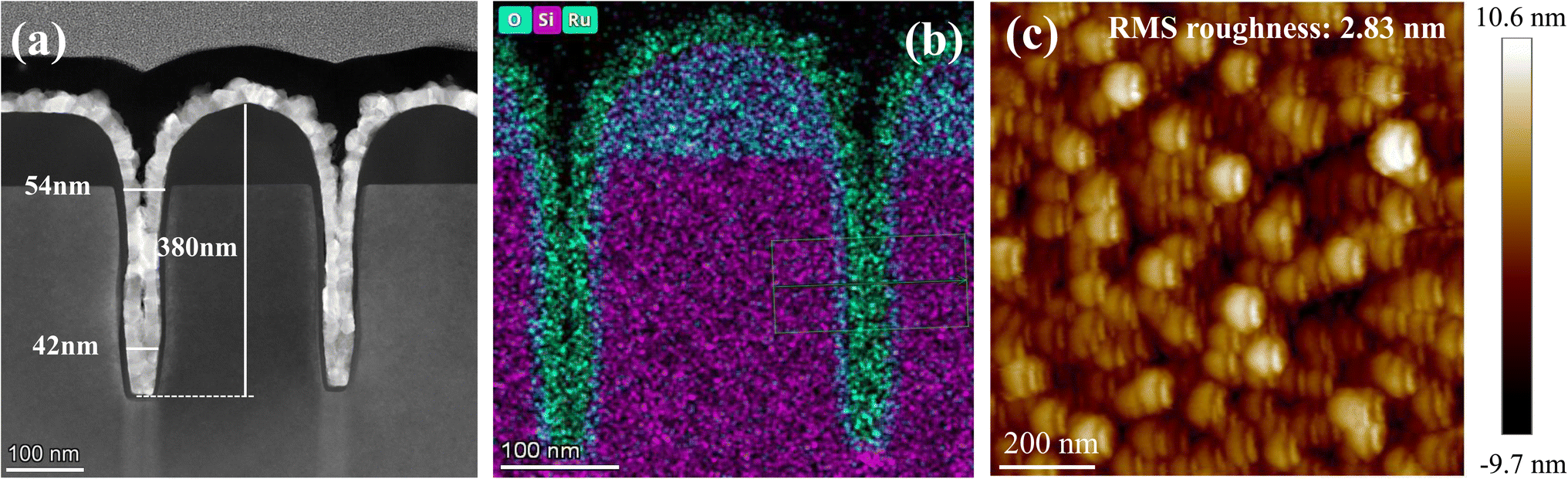 | ||
| Fig. 4 ALD Ru films for filling the nanoTSV arrays under the condition of deposition temperature of 300 °C, Ru(EtCp)2 pulse time for 3 s and the pulse time of O2 was fixed to 12 s. (a) TEM image of Ru filling for nanoTSV. (b) TEM elemental analysis. (c) AFM image (1 × 1 μm) of Ru film surface. | ||
The factors affecting the roughness were examined, and it was found that the growth temperature and Ru(EtCp)2 pulse time had an effect on roughness. Fig. 5a shows the roughness of the deposited film as a function of the Ru(EtCp)2 pulse time. The deposition temperature was fixed at 275 °C. With increase in the pulse time of Ru(EtCp)2, the roughness of Ru film first decreased, then increased and finally became stable. The minimum roughness was obtained at 2 s. Fig. 5b shows the roughness of the deposited film as a function of temperature. The deposition temperatures were varied from 260 to 310 °C, while the Ru(EtCp)2 pulse time was fixed at 2 s. With increase in temperature, the roughness of the deposited film was gradually decreasing and then increased. The minimum roughness of 0.8 nm was obtained at 275 °C. Fig. 5c shows the dependence of film thickness deposited in one cycle and the resistivity of the deposited films on the deposition temperature. The deposition temperatures were varied from 260 to 300 °C. The Ru(EtCp)2 pulse time was fixed at 2 s. With increase in temperature, the Ru films growth per cycle would increase; however, when the deposition temperature was greater than 275 °C, it would decrease. The resistivity had a minimum value of approximately 15 μΩ cm at 275 °C. This resistivity is similar to that reported in previous reports.13,36 The resistivity gradually increased with elevated temperatures, which correlated with the formation of RuO2 owing to oxidation reactions under high-temperature ALD conditions. These results are similar to those in a previous report on the effect of temperature on ALD Ru.20 It was reported that the resistivity of ALD Ru films increased at high temperatures, which was primarily attributed to the formation of RuO2.
 | ||
| Fig. 5 (a) The dependence of roughness on the Ru(EtCp)2 pulse time. (b) The dependence of roughness on the deposition temperature. (c) The dependence of GPC and resistivity of ALD Ru films on temperature. The pulse time of O2 was fixed at 12 s and the number of deposition cycles was 750. | ||
Fig. 6 shows that Ru films were deposited on SiO2 (10 nm-thick)/Si wafers at a deposition temperature and an Ru(EtCp)2 pulse time of 275 °C and 2 s, respectively. Other experimental conditions were the same as those mentioned above. Under the optimized experimental conditions, Ru grains were observed to be small, uniformly distributed, and densely packed, forming a continuous film as demonstrated by the SEM image in Fig. 6a. Fig. 6b shows the SEM side-view of the Ru film. The Ru film deposited over 750 cycles exhibited the thickness of approximately 45 nm, corresponding to a growth rate of 0.6 Å per cycle. This indicated that the self-limiting reaction had been achieved when the reaction temperature was 275 °C and the pulse time of Ru precursor was 2 s. Fig. 6c shows the AFM image of the Ru film. The measured surface roughness of the Ru film was 0.8 nm, representing the lowest value achieved in this study. This minimized roughness considerably enhanced the conformal filling capability of nanoTSV by reducing geometric shadowing effects during ALD.
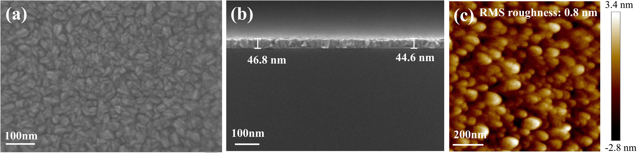 | ||
| Fig. 6 Plan-view (a) and side-view (b) scanning electron microscopy (SEM) images of Ru films deposited on 10 nm SiO2/Si substrates at 275 °C after 750 ALD cycles with an Ru(EtCp)2 pulsing time of 2 s and O2 exposure time of 12 s. (c) AFM image (1 × 1 μm) of the Ru film surface. | ||
Finally, the optimized experimental conditions were applied to fill the nanoTSV arrays, and the resultant arrays were analyzed (Fig. 7). Fig. 7a and b show the filling effect of the nanoTSV arrays. NanoTSV arrays were densely filled with 100% step coverage. The EDS analysis of the Ru film revealed no detectable oxygen signal, confirming the formation of pure Ru. This oxygen-free deposition was then corroborated by the elemental maps in Fig. 7c and f. The crystal structure of the Ru film was analysed by TEM. As can be seen in Fig. 7d, the TEM image revealed a polycrystalline structure, with lattice fringes corresponding to the hexagonal close-packed phase of metallic Ru. Previous studies have achieved either dense filling of microscale structures11 or conformal coverage in nanoscale features.13,14 However, this work achieves void-free Ru filling in ultrahigh aspect ratio nanoTSVs (30 nm width × 450 nm height), representing a critical advancement toward next-generation interconnects. The combined metrics of low resistivity and seamless filling position Ru as a promising candidate to replace conventional Cu-interconnects in advanced technology nodes.
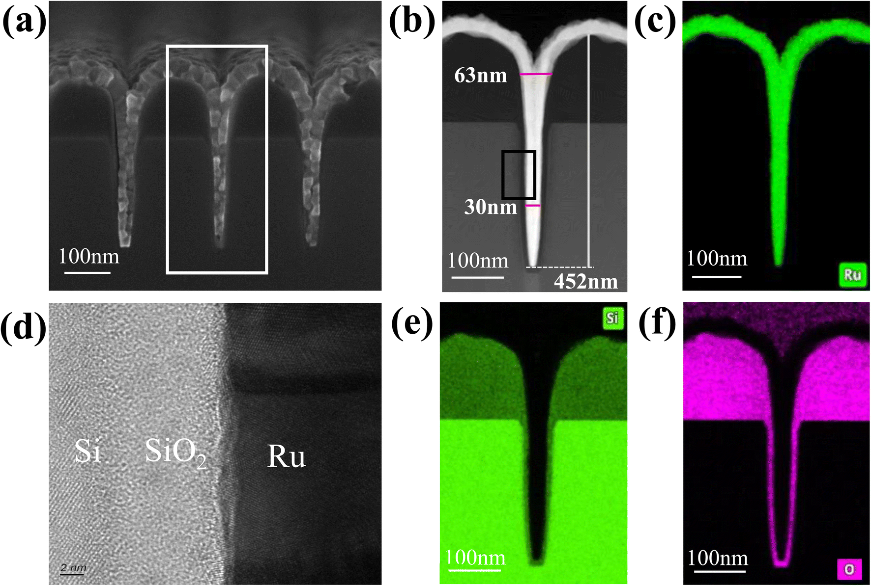 | ||
| Fig. 7 ALD Ru films for filling the nanoTSV arrays at a temperature of 275 °C, Ru(EtCp)2 pulse time of 2 s and O2 exposure time of 12 s. (a) Side-view SEM images of nanoTSV filled with Ru. (b) Side-view TEM images of nanoTSV filled with Ru. (c) Elemental analysis of Ru via TEM. (d) Lattice analysis via TEM. (e) Elemental analysis of Si via TEM. (f) Elemental analysis of O via TEM. | ||
4. Conclusions
In summary, Ru films were successfully deposited on SiO2 (10 nm-thick)/Si wafers by thermal ALD using Ru(EtCp)2 and oxygen at growth temperatures ranging from 260 °C to 310 °C, with the oxygen pulse time fixed at 12 s. The Ru film during one deposition cycle was saturated at 0.6 Å per cycle and had a resistivity of 15 μΩ cm. Elevated growth temperatures or insufficient Ru(EtCp)2 pulse times promoted RuO2 formation, resulting in increasing resistivity of the Ru film. When the growth temperature was 275 °C and the pulse time of Ru(EtCp)2 was 2 s, the Ru film had a minimum roughness of 0.8 nm, which was beneficial to the filling of nanoTSV. Finally, we achieved a dense filling and 100% step coverage for the nanoTSV arrays successfully. This indicates that the process is especially promising for the fabrication of Ru to replace Cu interconnects in advanced ICs.Data availability
The authors declare that the data supporting the findings of this study are available within the paper.Author contributions
Zhao Chen, Feifeng Huang and Biao Wang contributed equally to this work. Zhao Chen and Qiu Shao designed the experimental scheme and conducted the experiments. Biao Wang and Feifeng Huang analyzed the experimental data and optimized the experimental scheme. Qiancheng Wang performed TEM and SEM analyses on the experimental samples. Hongbin Chen performed XPS and AFM analyses on the experimental samples. Ming Ji helped supplement the XPS data and polish the manuscript. All the authors participated in the writing of the manuscript.Conflicts of interest
The authors do not have any possible conflict of interest.Acknowledgements
This work was supported by the National Natural Science Foundation of China (Grant No. 52305603), the National Key Research and Development Program of China (No. 2022YFB4602600), the Hunan Provincial Innovation Foundation for Postgraduate (No. CX20220406) and the Guangdong Basic and Applied Basic Research Foundation (2025A1515010847).References
- M. Breeden, V. Wang, R. Kanjolia, M. Moinpour, J. Woodruff, H. Simka and A. Kummel, Ru ALD With Bulk-Like Resistivity for Interconnects, in 2022 IEEE International Interconnect Technology Conference (IITC), IEEE, 2022, pp. 120–122 Search PubMed.
- J. J. Plombon, E. Andideh, V. M. Dubin and J. Maiz, Appl. Phys. Lett., 2006, 89, 113124 CrossRef.
- F. Gstrein, K. P. O’Brien, J. S. Clarke and D. Gall, Phys. Rev. B:Condens. Matter Mater. Phys., 2011, 84, 235423 CrossRef.
- D. Gall, J. Appl. Phys., 2020, 127, 050901 CrossRef CAS.
- K. Barmak, S. Ezzat, R. Gusley, A. Jog, S. Kerdsongpanya, A. Khaniya, E. Milosevic, W. Richardson, K. Sentosun, A. Zangiabadi, D. Gall, W. E. Kaden, E. R. Mucciolo, P. K. Schelling, A. C. West and K. R. Coffey, J. Vac. Sci. Technol., A, 2020, 38, 033406 CrossRef CAS.
- I. Ciofi, A. Contino, P. J. Roussel, R. Baert, V. H. Vega-Gonzalez, K. Croes, M. Badaroglu, C. J. Wilson, P. Raghavan, A. Mercha, D. Verkest, G. Groeseneken, D. Mocuta and A. Thean, IEEE Trans. Electron Devices, 2016, 63, 2496 Search PubMed.
- S. Datta, R. Pandey, A. Agrawal, S. K. Gupta and R. Arghavani, Impact of contact and local interconnect scaling on logic performance, in 2014 Symposium on VLSI Technology (VLSI-Technology): Digest of Technical Papers, IEEE, 2014, pp. 1–2 Search PubMed.
- J. M. Hwang, S.-M. Han, H. Yang, S. Yeo, S.-H. Lee, C. W. Park, G. H. Kim, B. K. Park, Y. Byun, T. Eom and T.-M. Chung, J. Mater. Chem. C, 2021, 9, 3820–3825 RSC.
- M. M. Minjauw, J. Dendooven, B. Capon, M. Schaekersb and C. Detavernier, J. Mater. Chem. C, 2015, 3, 132–137 RSC.
- R. Müller, L. Ghazaryan, P. Schenk, S. Wolleb, V. Beladiya, F. Otto, N. Kaiser, A. Tünnermann, T. Fritz and A. Szeghalmi, Coatings, 2018, 8, 413 CrossRef.
- M. Y. Wang, J. H. Wang, L. Jin, T. Yu and D. Q. Yu, Vacuum, 2024, 221, 112927 CrossRef CAS.
- T. E. Hong, S. H. Choi, S. Yeo, J. Y. Park, S. H. Kim, T. Cheon, H. Kim, M. K. Kim and H. Kim, ECS J. Solid State Sci. Technol., 2013, 2, P47–P53 CrossRef CAS.
- Y. Kotsugi, S. M. Han, Y. H. Kim, T. Cheon, D. K. Nandi, R. Ramesh, N. K. Yu, K. Son, T. Tsugawa, S. Ohtake, R. Harada, Y. B. Park, B. Shong and S. H. Kim, Chem. Mater., 2021, 33, 5639–5651 CrossRef CAS.
- E. C. Ko, J. Y. Kim, H. Rhee, K. M. Kim and J. H. Han, Mater. Sci. Semicond. Process., 2023, 156, 107258 CrossRef CAS.
- K. Croes, C. Adelmann, C. J. Wilson, H. Zahedmanesh, O. V. Pedreira, C. Wu, A. Lesniewska, H. Oprins, S. Beyne, I. Ciofi, D. Kocaay, M. Stucchi and Z. Tokei, Interconnect metals beyond copper: Reliability challenges and opportunities, in 2018 IEEE International Electron Devices Meeting (IEDM), IEEE, 2018, pp. 5–3 Search PubMed.
- Y.-H. Kim, M. Kim, Y. Kotsugi, T. Cheon, D. Mohapatra, Y. Jang, J. Bae, T. E. Hong, R. Ramesh, K. An and S. Kim, Adv. Funct. Mater., 2022, 32, 2206667 CrossRef CAS.
- D. Z. Austin, M. A. Jenkins, D. Allman, S. Hose, D. Price, C. L. Dezelah and J. F. Conley Jr, Chem. Mater., 2017, 29, 1107–1115 CrossRef CAS.
- C. T. Nguyen, J. Yoon, R. K. Khan, B. Shong and H.-B.-R. Lee, Appl. Surf. Sci., 2019, 488, 896–902 CrossRef CAS.
- D. S. Kwon, C. H. An, S. H. Kim, D. G. Kim, J. Lim, W. Jeon and C. S. Hwang, J. Mater. Chem. C, 2020, 8, 6993–7004 RSC.
- W. H. Kim, S. J. Park, D. Y. Kim and H. Kim, J. Korean Phys. Soc., 2009, 55, 32–37 CrossRef CAS.
- O. K. Kwon, S. H. Kwon, H. S. Park and S. W. Kang, Electrochem. Solid-State Lett., 2004, 7, C46–C48 CrossRef CAS.
- T. Park, D. Choi, H. Choi and H. Jeon, Phys. Status Solidi A, 2012, 209, 302–305 CrossRef CAS.
- F. Papadatos, S. Consiglio, S. Skordas, E. T. Eisenbraun and A. E. Kaloyeros, J. Mater. Res., 2007, 22, 2254–2264 CrossRef CAS.
- M. G. Kozodaev, Y. Y. Lebedinskii, A. G. Chernikova, E. V. Korostylev, A. A. Chouprik, R. R. Khakimov, A. M. Markeev and C. S. Hwang, J. Chem. Phys., 2019, 151, 204701 CrossRef CAS PubMed.
- S. J. Park, W. H. Kim, H. B. R. Lee, W. J. Maeng and H. Kim, Microelectron. Eng., 2008, 85, 39–44 CrossRef CAS.
- J. M. Hwang, S. M. Han, H. Yang, S. Yeo, S. H. Lee, C. W. Park, G. H. Kim, B. K. Park, Y. Byun, T. Eom and T. M. Chung, J. Mater. Chem. C, 2021, 9, 3820–3825 RSC.
- T. Aaltonen, P. Alén, M. Ritala and M. Leskelä, Chem. Vap. Deposition, 2003, 9, 45–49 CrossRef CAS.
- D. Z. Austin, M. A. Jenkins, D. Allman, S. Hose, D. Price, C. L. Dezelah and J. F. Conley, Chem. Mater., 2017, 29, 1107–1115 CrossRef CAS.
- S. S. Yim, D. J. Lee, K. S. Kim, S. H. Kim, T. S. Yoon and K. B. Kim, J. Appl. Phys., 2008, 103, 113509 CrossRef.
- S. S. Yim, D. J. Lee, K. S. Kim, M. S. Lee, S. H. Kim and K. B. Kim, Electrochem. Solid-State Lett., 2008, 11, K89–K92 CrossRef CAS.
- J. L. Lu and J. W. Elam, Chem. Mater., 2015, 27, 4950–4956 CrossRef CAS.
- O. K. Kwon, J. H. Kim, H. S. Park and S. W. Kang, J. Electrochem. Soc., 2004, 151, G109–G112 CrossRef CAS.
- O. K. Kwon, S. H. Kwon, H. S. Park and S. W. Kang, J. Electrochem. Soc., 2004, 151, C753–C756 CrossRef CAS.
- D. J. Lee, S. S. Yim, K. S. Kim, S. H. Kim and K. B. Kim, Electrochem. Solid-State Lett., 2008, 11, K61–K63 CrossRef CAS.
- S. H. Kwon, O. K. Kwon, J. H. Kim, S. J. Jeong, S. W. Kim and S. W. Kang, J. Electrochem. Soc., 2007, 154, H773–H777 CrossRef CAS.
- J. Y. Kim, D. S. Kil, J. H. Kim, S. H. Kwon, J. H. Ahn, J. S. Roh and S. K. Park, J. Electrochem. Soc., 2012, 159, H560–H564 CrossRef CAS.
| This journal is © The Royal Society of Chemistry 2025 |