
 Open Access Article
 This Open Access Article is licensed under a
 Creative Commons Attribution 3.0 Unported Licence
Elucidating the role of oxidation in two-dimensional silicon nanosheets†
Jeremy B.
Essner
 a,
Abhijit
Bera
a,
Maharram
Jabrayilov
a,
Abhishek
Chaudhari
a,
Benjamin T.
Diroll
c,
Julia V.
Zaikina
b and
Matthew G.
Panthani
*a
a,
Abhijit
Bera
a,
Maharram
Jabrayilov
a,
Abhishek
Chaudhari
a,
Benjamin T.
Diroll
c,
Julia V.
Zaikina
b and
Matthew G.
Panthani
*a
aDepartment of Chemical and Biological Engineering, Iowa State University, Ames, Iowa 50011, USA. E-mail: panthani@iastate.edu
bDepartment of Chemistry, Iowa State University, Ames, Iowa 50011, USA
cCenter for Nanoscale Materials, Argonne National Laboratory, 9700 S. Cass Avenue, Lemont, IL 60639, USA
First published on 16th December 2024
Abstract
We report a synthetic protocol that yields hydrogen-terminated 2D silicon nanosheets with greatly reduced siloxane (e.g., Si–O–Si, OxSi) content. These nanosheets displayed weak, broad photoluminescence centered near 610 nm with a low absolute photoluminescence quantum yield (as low as 0.2%). By intentionally oxidizing the nanosheets, the photoluminescence peak emission wavelength blueshifted to 510 nm, and the quantum yield increased by more than an order of magnitude to 8.5%. These results demonstrate that oxidation of 2D silicon nanosheets modulates the material's bandgap and suggests that previously reported photoluminescence properties for this material resulted, in part, from oxidation.
New conceptsA new synthetic route for 2D silicon nanosheets that produces hydrogen-terminated 2D Si with greatly reduced siloxane (e.g., Si–O–Si, OxSi) content is reported. The 2D silicon nanosheets prepared by this route are effectively non-luminescent with an absolute quantum yield as low as 0.2% while oxidation of the Si monolayers leads to photoluminescent quantum yields over 8%. These results reveal that the photoluminescence previously observed for hydrogen-terminated 2D Si arises from oxidation of the Si backbone, providing a pathway for bandgap engineering in these materials through controlled oxidation. |
In the last decade, the demand for computational power, communication, and data storage has skyrocketed. As transistors—the backbone of microelectronic systems—reach their physical size limits and energy consumption continues to rise, alternative methods for information transmission and storage have become critical.1,2 One promising solution is to use electromagnetic radiation, particularly in the visible to infrared spectrum, as the information carrier. By integrating photonic and optoelectronic devices within microchips, more energy-efficient information transmission could be achieved.3 However, a significant challenge remains: finding materials that not only emit light efficiently (luminesce) but also integrate seamlessly with current microelectronic infrastructure.4
Layered two-dimensional (2D) materials are a rising class of material that display intriguing (photo)physical and electronic properties upon thinning to few-layer stacks of individual monolayers,5,6 positioning these materials as prime candidates for next-generation photonic and optoelectronic applications. Indeed, since the discovery of graphene in 2004, 2D materials, such as transition-metal (di)chalcogenides, hexagonal boron nitride, phosphorene, and MXenes, have garnered growing attention in the scientific community as new active materials in photonic and optoelectronics applications, such as quantum emitters/detectors, lasers, light emitting diodes, optical modulators, photovoltaics, and photodetectors, due to their tunable bandgaps, high electrical conductivity, non-linear optics, strong in-plane bonding (i.e., mechanical strength), flexibility, and tailorable surface chemistry.6–11 While these materials show promise for next-generation photonic and optoelectronic applications, they often suffer from poor, or even non, compatibility with the current microelectronic infrastructure.
As the heart of microelectronics is silicon, materials based on group IV elements are ideal candidates for next-generation photonic and optoelectronic applications due to their complementary metal–oxide semiconductor compatibility, which allows facile integration into current microelectronic infrastructures.12–16 Unfortunately, the group IV semiconductors possess indirect bandgaps and are, thus, terribly inefficient at emitting light. However, this inefficient luminescence can be overcome by confining at least one physical dimension of the group IV semiconductors to the nanoscale making (luminescent) 2D materials based on group IV elements (i.e., Xenes, Xanes) of keen interest for next-generation photonic and optoelectronic applications, and beyond.17–25 For example, 2D germanium has been explored in diode and photodetector applications due to its predicted high electron mobility and direct, tunable bandgap.22,23,26 2D silicon (e.g., silicene, silicane, siloxene) is of particular interest as the active material in photonic and optoelectronic devices due to its tunable surface chemistry,27,28 observed photo- and electro-luminescence,24,29–31 high charge carrier mobilities,32 and non-linear optical properties.33 Additionally, 2D silicon has shown promise in numerous other technologies such as batteries,34 supercapacitors,35 neuromorphic devices,36 and biomedical applications.37 However, before 2D Group IV materials can be successfully deployed in commercial applications, particularly optoelectronic devices, improved understandings of their structure–property relationships and light–matter interactions are required.
Atomically thin, freestanding 2D silicon (111) nanosheets (e.g., silicane) represent an ideal foundation to build these understandings on due to (1) the terrestrial abundance of silicon and (2) the vast library of knowledge that already exists for bulk Si surfaces, such as (111) oriented Si.28 However, despite freestanding 2D silicon nanosheets (SiNSs) being first reported over 150 years ago,38 little progress has been made towards such understandings since.39–44 Further, the sparce work has introduced conflicting conclusions in the literature record on the structural nature of the 2D Si monolayers. Specifically, whether the individual Si monolayers are fully hydrogen terminated (i.e., silicane/layered polysilane),42–44 50% hydroxylated (i.e., Wöhler/Weiss siloxene),38,41 contain siloxanes (i.e., Kautsky siloxene),39,40 or chlorine termination.43 This variability in reported structure stems, in part, from the inconsistencies in preparation methods, with materials often being insufficiently characterized when experimental parameters are changed. For instance, these materials are typically prepared from the layered Zintl phase, calcium disilicide (CaSi2), through topotactic deintercalation of Ca2+ by (concentrated) aqueous HCl,39–44 however, the employed CaSi2 purity, atmospheric composition, deintercalation temperature, and product purification vary widely with minimal conclusions drawn in relation to these differing experimental parameters.
Recently, our group provided insight into this long-standing debate by demonstrating that impurities in CaSi2 have impacted interpretation of SiNS structural characterizations and that the 2D Si monolayers consist of a buckled Si backbone terminated with randomly distributed hydrogen, chlorine, and hydroxyl groups in an approximate ratio of 70![[thin space (1/6-em)]](https://www.rsc.org/images/entities/char_2009.gif) :20:10, respectively.29,45 We note that this assessed surface termination is for SiNSs prepared under inert atmosphere at temperatures below −30 °C. The literature suggests that SiNSs prepared in air or at higher temperatures possess a different ratio of these groups;43,46 however, exact ratios and correlations to these experimental parameters have yet to be reported. We also demonstrated that, while infrared spectroscopy indicates the presence of siloxanes (Si–O–Si) via an intense stretch at approximately 1050 cm−1, the intensity of this mode arises from a relatively large induced dipole moment, not a high concentration of siloxane groups within the material.29 While the quantity of oxidation within the SiNSs in the form of siloxane is minute, its exact origin (e.g., oxygen, water) and subsequent impact on observed material properties remains unaddressed. Indeed, the presence of oxidation within the material has only further complicated structure–property understandings, such as the origin of the material's room-temperature, cyan (500 nm) photoluminescence (PL) and PL quantum yields (ΦPL) of nearly 10%.29,43,47 Historically, the origin of this PL has been attributed to chemical quantum confinement of silicon by oxygen; however, this conclusion has been intensely debated.48–51
:20:10, respectively.29,45 We note that this assessed surface termination is for SiNSs prepared under inert atmosphere at temperatures below −30 °C. The literature suggests that SiNSs prepared in air or at higher temperatures possess a different ratio of these groups;43,46 however, exact ratios and correlations to these experimental parameters have yet to be reported. We also demonstrated that, while infrared spectroscopy indicates the presence of siloxanes (Si–O–Si) via an intense stretch at approximately 1050 cm−1, the intensity of this mode arises from a relatively large induced dipole moment, not a high concentration of siloxane groups within the material.29 While the quantity of oxidation within the SiNSs in the form of siloxane is minute, its exact origin (e.g., oxygen, water) and subsequent impact on observed material properties remains unaddressed. Indeed, the presence of oxidation within the material has only further complicated structure–property understandings, such as the origin of the material's room-temperature, cyan (500 nm) photoluminescence (PL) and PL quantum yields (ΦPL) of nearly 10%.29,43,47 Historically, the origin of this PL has been attributed to chemical quantum confinement of silicon by oxygen; however, this conclusion has been intensely debated.48–51
We previously simulated band structures of fully hydrogen-terminated 2D Si (e.g., Si32H32) and various oxidized forms of this parent structure using DFT.30 Additionally, our collaborators simulated band structures of 2D Si with different ratios of hydrogen and chlorine termination.45 These studies showed that fully hydrogen-terminated SiNSs possess a quasi-direct band structure with direct and indirect bandgap energies (Eg's) of approximately 2.26–2.1 eV and 2.16–2.05 eV, respectively,29,30,45 suggesting this material should display weak PL between approximately 550 and 600 nm. Additional simulations of oxidized SiNS structures revealed a shift to a direct bandgap material with an Eg of 2.14 eV (579 nm) upon the formation of only one siloxane group (Si–O–Si) per every 32 Si atoms.30 Further formation of siloxane groups about a central Si atom (i.e., O2SiH, O3SiH) led to slightly lower Eg (<2.11 eV; 588–600 nm), while increased oxidation in other configurations led to inconsistent trends in Eg. However, in all instances, increasing oxidation resulted in direct bandgaps. These previously reported simulations suggest that oxidation of SiNSs will produce a concomitant red shift and increase in PL, relative to fully hydrogen terminated SiNSs, providing a viable route for band structure engineering of these materials via controlled oxidation.
Herein, we provide evidence that dissolved oxygen present in the aqueous HCl is the primary source of the oxidation that is observed in freshly prepared, hydrogen-terminated SiNSs (H-SiNSs), thus providing a synthetic route for SiNSs free of siloxane groups (Scheme 1). We must clarify that the H-SiNS composition is nominally SiH0.7Cl0.2(OH)0.1 and we only refer to the material as H-SiNSs for simplicity. We found that these H-SiNSs exhibit weak PL (ΦPL < 0.6%) centered near 610 nm, with this feature attributed to the recently elucidated surface composition for H-SiNSs (SiH0.7Cl0.2(OH)0.1), a conclusion that is reinforced by previously reported band structure simulations.45 Furthermore, we also found that oxidation is responsible for the cyan (500 nm) photoluminescence (ΦPL = 8–10%) often observed. This conclusion is supported by correlated increases in oxygen content in the material (assessed by FTIR and EDX spectroscopies) and ΦPL (schematically shown in Scheme 1).
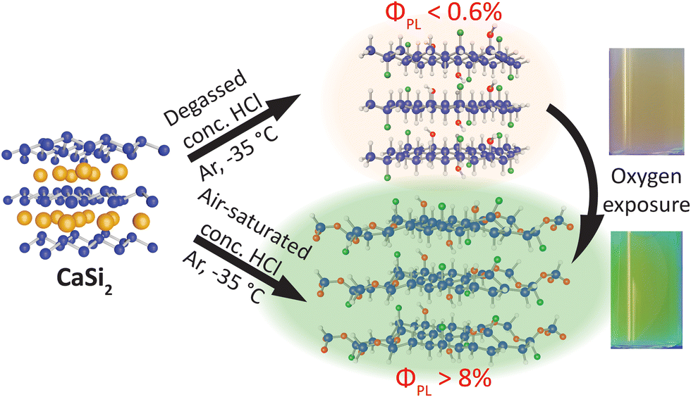 | ||
| Scheme 1 Deintercalation of the Zintl phase precursor, CaSi2, using degassed HCl yields a weakly red emitting material with a peak PL centered at 610 nm and a photoluminescent quantum yield (ΦPL) as low as 0.2% (highest of 0.6%). Upon oxygen exposure, either in the form of dried air or dissolved gas in the HCl, the photoluminescence effectively “turns on” leading to at least a 14-fold increase in ΦPL to over 8% and a 100 nm blueshift in peak PL to approximately 516 nm. | ||
Results and discussion
Synthesis of silicon nanosheets
We prepared the calcium disilicide (CaSi2) precursor and deintercalated silicon nanosheets (SiNSs) following our previously reported protocols.30,52 Comprehensive descriptions of the experimental details are provided in the methods section of the ESI.† Briefly, we synthesized the CaSi2 precursor via a hydride approach and prepared the SiNSs by deintercalating the CaSi2 with concentrated HCl at −35 °C under inert atmosphere (e.g., Ar).52 We confirmed the phase purity of the CaSi2 precursor with pXRD (Fig. S1, ESI†). We generated the H-SiNSs by rigorously degassing the HCl prior to the addition of CaSi2; the degassing protocol consisted of bubbling Ar through the HCl for at least 24 h, followed by four freeze–pump–thaw cycles. Additionally, we employed air-free filtration glassware to isolate the SiNSs from the HCl before transferring the glassware assembly to a glovebox filled with nitrogen for further purification. The reproducibility of this approach was confirmed with pXRD, FTIR, and PL measurements (Fig. S2 and S3, ESI†). Lastly, to oxidize the SiNSs, we injected incremental volumes of dried air (see ESI†) into degassed, anhydrous acetonitrile (ACN) dispersions of SiNSs under inert atmosphere and kept the dispersions under magnetic stirring for 48 h. All samples are denoted by the oxygen (O2):Si mole ratio (reported in parts per hundred, pph), where the reported values represent the amount of molecular oxygen intentionally exposed to the SiNSs (0.0, 0.2, 0.5, 1.1, 2.2, 4.4, and 8.4 pph); we use the “pph” nomenclature instead of atom percent to avoid confusion with ΦPL values. Note, the 0.2 pph sample is the sample prepared in air-saturated HCl; see the ESI† for details on how we arrived at this value. We characterized the samples with powder X-ray diffraction (pXRD), Fourier-transform infrared (FTIR) spectroscopy, scanning electron microscopy (SEM), energy-dispersive X-ray (EDS) spectroscopy, and optical spectroscopies, with confirmation of SiNS oxidation achieved with FTIR and EDS. We note that all solvents employed in this work were anhydrous and were degassed prior to use, unless otherwise noted, to minimize unintentional oxidative effects.
Structural characterizations
We assessed the impact of oxygen exposure on the SiNSs’ long-range structure with pXRD and SEM. Exposing the SiNSs to increasing quantities of dried air (0.2–8.4 pph O2:Si) led to the emergence of bimodal diffraction associated with the interlayer nanosheet spacing (2θ ≈ 13.5°; (001) peak), which eventually separated into two distinct peaks centered at 2θ ≈ 10° and 2θ ≈ 14°, corresponding to d spacings of approximately 8.3 and 6.3 Å, respectively (Fig. 1(A) and inset). The full diffraction patterns are provided in the ESI† (Fig. S4). Note, we normalized the diffraction patterns to the (001) peak and deconvoluted these patterns between 2θ = 5–20° to obtain the d-spacing values (Fig. S5, ESI†). The diffraction peak centered at 6.3 Å for all samples is consistent with previously reported DFT simulations that predicated an interlayer spacing of 6.2 Å for SiH0.7Cl0.2(OH)0.1.45 Additionally, our previous DFT simulations of thermodynamically relaxed, fully hydrogen-terminated 2D Si with different configurations of Si–O–Si bond formation revealed that oxidation of the SiNS backbone induced structural strain that further buckled the Si network;30 this buckling impacted atomic configurations (e.g., bond angles) over five Si sites away for just one in 32 Si atoms oxidized to OxSiH (see supporting information of ref. 30). Given this, we tentatively attribute the emergence of the diffraction peak centered near 2θ ≈ 10° upon increasing oxygen exposure to buckling of the Si backbone from Si–O–Si bond formation (i.e., oxidation), which increases the interlayer spacing to approximately 8.3 Å. Based on this tentative conclusion, the broadness of the peak centered at 8.3 Å also suggests a random distribution of OxSiH groups within the Si backbone, where x = 0–3. Therefore, the bimodal distribution observed for the interlayer spacing indicates that the large sheet stacks consist of non-oxidized SiNSs, nominally of the composition SiH0.7Cl0.2(OH)0.1, and SiNSs with a broad range of larger interlayer spacings arising from varying degrees of oxidation of the SiNSs. Even though we mildly exfoliated the SiNSs via bath sonication prior to intentional oxidation and kept the dispersions under magnetic stirring during the oxidation period, the poor dispersibility of these samples hinders complete exfoliation, thus restricting the accessibility of O2 to the inner most monolayers and resulting in a heterogenous mixture of variably oxidized and non-oxidized 2D Si materials. Lastly, the results show that pXRD can be used as a qualitative gauge for oxidation of SiNSs. That is, observed peak asymmetry, in the form of a shoulder, on the higher d spacing side of the peak at 6.3 Å is indicative of early-stage oxidation of the outer monolayers or monolayer edges/corners.
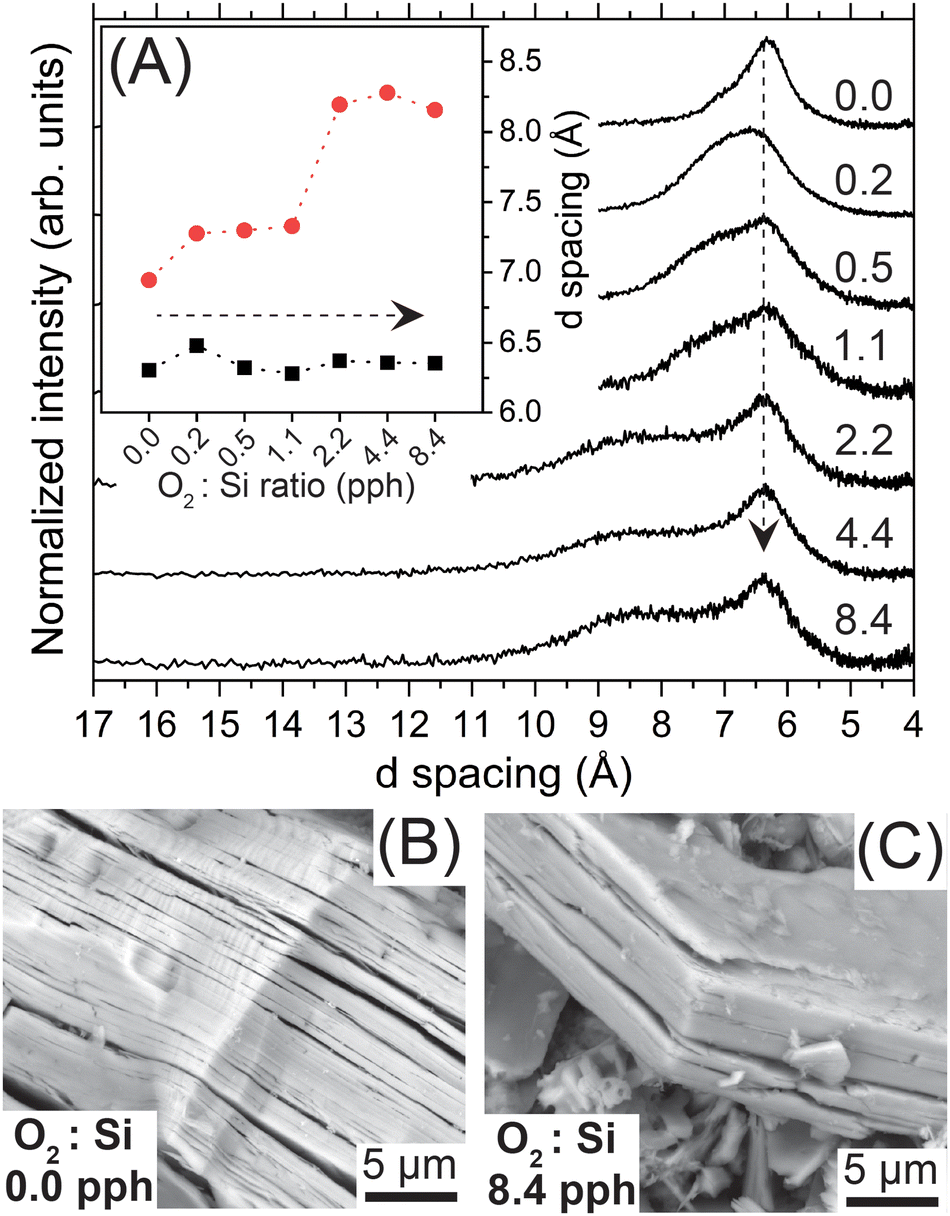 | ||
| Fig. 1 (A) pXRD of the SiNSs exposed to increasing quantities of oxygen. The d spacing extracted from deconvolution of the pXRD patterns is provided in the inset. The dashed arrows indicate increasing oxygen exposure. Representative SEM images of (B) SiNSs generated in degassed HCl (0.0 pph O2:Si ratio) and (C) SiNSs exposed to the highest quantity of oxygen in this study (8.4 pph O2:Si ratio). | ||
To assess whether the hypothesized backbone buckling translated to macroscopic changes in the (stacks of) nanosheets, we imaged the SiNS samples with SEM. Representative SEM images of the 0.0 pph O2:Si sample and the SiNS sample exposed to the highest quantity of oxygen (8.4 pph O2:Si) are provided in panels (B) and (C) of Fig. 1, respectively. The macroscopic features of the SiNS samples generated in degassed HCl (0.0 pph O2:Si; Fig. 1(B) and Fig. S6(A), ESI†) are consistent with those observed for samples previously prepared in our lab (i.e., air-saturated HCl (approx. 0.2 pph O2:Si)).29,30,45 Conversely, an apparent decrease in nanosheet (stack) size is observed for the sample exposed to the highest quantity of oxygen (Fig. 1(C) and Fig. S6(C), ESI†). A control study, in which the SiNSs prepared in air-saturated HCl (0.2 pph O2:Si) were bath sonicated in ACN, revealed that the exfoliation of the SiNS stacks during the bath sonication step (Fig. S6(B) and S6(C), ESI†) caused the observed size reduction. The observed size decreases in the sheet stack thickness and nanosheets’ lateral dimensions are attributed to improved exfoliation of the sheet stacks between individual monolayers and along grain boundaries that were present in the polycrystalline precursor, respectively. While we currently attribute the origin of the size decrease to the above, we cannot rule out mild sonication providing sufficient energy to cleave the weak Si–Si bonds (∼53 kcal mole−1) of the nanosheet. Regardless, the O2 exposure explored in this study did not markedly alter the macroscopic structure of the SiNSs (stacks).
We initially confirmed that exposure of the SiNSs to oxygen led to oxidation of the material with SEM-EDS analyses. While the oxygen content cannot be rigorously quantified with EDS due to oxygen in the carbon mounting tab and its ubiquitous presence (in minute quantities), regardless of employing stringent air-free conditions, increasing exposure to molecular oxygen clearly led to increasing oxygen content in the SiNSs (Table S1 and Fig. S7(A), ESI†). Representative SEM images and EDS data that Fig. S7 (ESI†) originates from are provided in Fig. S8 and S9 (ESI†). We also corrected the elemental composition for both (i) oxygen contributions from the carbon mounting tab using the C:O ratio determined from analysis of a bare mounting tab (Fig. S7(B), ESI†) and (ii) residual calcium chloride (CaCl2) in the sample (Fig. S7(C), ESI†), as this byproduct is frequently observed in samples due to incomplete removal during the washing step.29,45 The as-collected and corrected values are all tabulated in Table S1 (ESI†). We recognize that such corrections are based on many assumptions, however, the trends observed for the atomic percent (at%) of Si, O, and Cl remain essentially identical throughout these analyses. Therefore, the observed increase and decrease in O and Cl, respectively, are not artifacts of the sample or measurement. We also calculated the Cl:Si atomic ratio to further assess if the observation in decreased Cl is attributable to a real change in chlorine termination and is not a product of the increasing oxygen content (Fig. S7(D), ESI†; we scaled the ratio by a factor of six for improved clarity. For the 0.0 pph O2:Si sample, the Cl:Si atomic ratio is consistent with previously reported ratios of 1–2 terminating Cl atoms per every 6 Si atoms;45 however, a correction for residual CaCl2 had not been performed in our previous work. Thus, the corrected Cl:Si atomic ratios that we determined for the 0.2 pph O2:Si sample produced here and our previous sample45 are lower than the value we previously reported (approximately 0.8 Cl per 6 Si vs. 1.0 Cl per 6 Si). We note that previous characterizations with solid-state NMR yielded a ratio of 1.2 Cl per 6 Si;45 in these measurements, residual CaCl2 does not contribute to this ratio. We attribute the discrepancy between EDS and NMR to the brief air exposure (<15 min) that occurred when the previously reported samples were characterized with SEM. Conversely, in this work, we placed the samples in a specially designed sample holder capable of maintaining a controlled environment from a glovebox to within the SEM. Given this difference in sample treatment, the above analysis indicates that Cl termination is rapidly lost upon air (O2) exposure, consistent with a previous report on the stability of Cl on Si(111).53 Conversely, chlorinated Si(111) surfaces have been reported to be quite air stable,54,55 however, partial chlorination and Si–Cl bonds on step edges are more reactive.55 Therefore, we attribute the observed reactivity of Si–Cl in the SiNSs to the low Cl content and Si–Cl groups present along the edges. The instability of the Si–Cl bonds in the SiNSs is further confirmed by the drop in the Cl:Si atomic ratio to 0.5 Cl per 6 Si upon increasing the O2:Si ratio to 0.5 pph. Further increasing the O2:Si ratio to 2.2 and then 8.4 pph did not lead to any additional changes in the Cl:Si atomic ratio. We attribute this trend to the outer most nanosheets within a stack losing their Cl termination while those terminations deep within a stack remain intact due to inaccessibility by O2; such a conclusion is consistent with the conclusions drawn by pXRD. Overall, these results indicate that chlorine termination is lost during oxidative processes by molecular oxygen. Therefore, we anticipate that the 0.0 pph O2:Si sample will have an even higher Cl:Si atomic ratio than the previously assessed 1.2 Cl per 6 Si since these samples contained higher levels of oxidation compared to the 0.0 pph O2:Si sample (as assessed by FTIR); solid-state NMR characterizations are currently underway to confirm this hypothesis.
We further characterized the SiNSs with FTIR spectroscopy to confirm oxidation of the SiNSs and better understand the local chemical environment. FTIR spectra highlighting key differences between 0.0 pph O2:Si (degassed HCl) and 0.2 pph O2:Si (air-saturated HCl) are provided in Fig. 2(A), while spectra highlighting specific OxSi(–H) vibrational modes for increasing oxygen exposure are provided in Fig. 2(B). Note, spectra of the full wavenumber range collected are provided in Fig. S10(A) (ESI†). In general, the FTIR spectral profiles are consistent with previous samples generated in our lab, where the SiNS surface consists of –H, –OH, and –Cl functionalities.29,30,52 Specifically, Si–H stretching for Si bonded to three other Si atoms near 2100 cm−1, Si–H stretching for Si bonded to at least one oxygen atom on the red-edge shoulder of the 2100 cm−1 peak, Si–H stretching for Si bonded to three oxygen atoms at approximately 2200 cm−1, Si–O–Si asymmetric stretching between 950–1200 cm−1, Si–H bending, including SiH3/SiH2, at approximately 900 cm−1, 670 cm−1, 630 cm−1, and 512 cm−1, OxSiH bending between 810–910 cm−1, Si–O symmetric stretching (including Si–O within Si–OH) at 800 cm−1, O–H stretching from Si–OH at approximately 3600 cm−1, and a Si–Cl vibration at 570 cm−1. Our previous DFT simulations support these assignments.29 The key differences between the 0.0 pph O2:Si (degassed HCl) and 0.2 pph O2:Si (air-saturated HCl) samples, as well our previously published results,29,30 are the intensity and spectral shape of the Si–O–Si asymmetric stretch, as well as the observance of vibrations ascribed to SiH3 and SiH2 stretching (2250–2350 cm−1) and bending (875–950 cm−1) modes; these differences indicate that SiH3 features, and to a lesser extent SiH2, quickly oxidize upon oxygen exposure. The reproducibility of these features for different 0.0 pph O2:Si samples is highlighted in panels (B) and (C) of Fig. S3 (ESI†). Further increasing the oxygen exposure resulted in the following changes to Si–O vibrations: (i) the asymmetric stretch of Si–O–Si (approximately 1050 cm−1) markedly increased, (ii) two peaks between 810–910 cm−1 from OxSiH bending grew in, and (iii) a weak vibration near 2250 cm−1 from Si–H stretching of O3SiH emerged (Fig. 2(B), 3(A), 3(B) and Fig. S10(A), ESI†). Additionally, spectral shifts in peaks arising from Si–H stretching and bending are observed (Fig. S10(B), ESI†), changes that are consistent with increasing oxidation and decreasing Cl termination.56,57 Note, the vibrations centered near 3400 and 1650 cm−1 arise from adsorbed water, not –OH surface termination, features often misassigned in the literature. Additionally, any observed CHx stretching is attributed to residual organic solvent on the ATR crystal after cleaning, as CHx stretching is not always observed. In the case of the 0.0 pph O2:Si sample, however, the observed CHx stretching arises from the mineral oil that we immersed the sample in to minimize potential oxidation during data collection (<30 s air exposure prior to collection; <5 min total air exposure). As all other samples were exposed to air during data collection, we conducted a time-dependent FTIR study of the 0.0 pph O2:Si sample not immersed in oil (Fig. S11(A), ESI†). This study revealed that rapid, albeit minor, oxidation of the SiNSs occurred within 30 s of air exposure; however, we did not observe further oxidation via FTIR after an additional 15 min of air exposure. Even after 48 h of wet air exposure in a capped vial, the sample remained less oxidized than the sample generated in air-saturated HCl (0.2 pph O2:Si sample). Further, the minor spectral shifts observed in Si–H stretching and bending modes are consistent with slight oxidation (Fig. S11(B), ESI†). Thus, the results show that the brief air exposure that occurred during data collection is unlikely to result in a measurable level of oxidation in samples already partially oxidized. Additionally, the results indicate that once the SiNSs are partially oxidized they are relatively stable in powder form. Lastly, the intensity of the Si–Cl vibration weakened slightly with increasing oxygen exposure, suggesting a loss of chlorine termination (Fig. S10(A), ESI†), which is consistent with our conclusions from the EDS analyses.
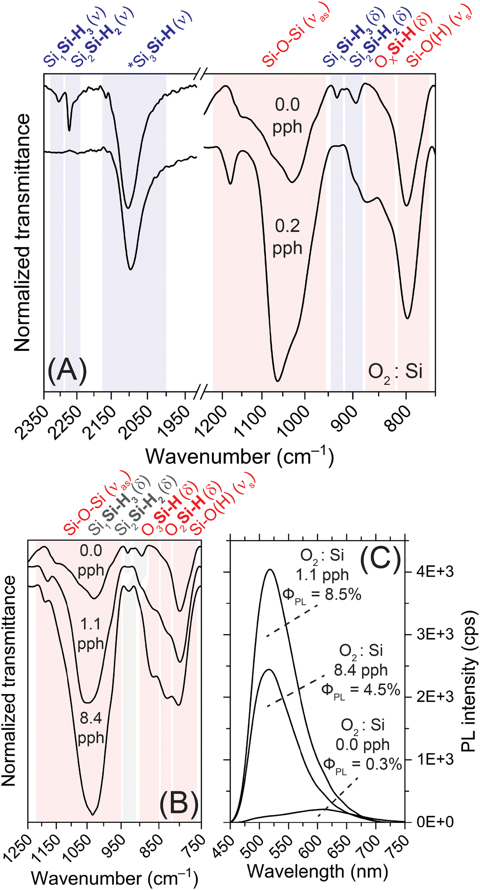 | ||
| Fig. 2 (A) FTIR spectra of SiNSs prepared in degassed HCl (0.0 pph O2:Si) or air-saturated HCl (0.2 pph O2:Si). (B) FTIR spectra of select SiNS samples showing changes observed to oxygen-related vibrations upon increasing oxygen exposure. (C) Corresponding PL spectra for the samples shown in panel (B), revealing a marked increase in PL (ΦPL of 0.3% to ΦPL of 8.5%) upon slight oxygen exposure, and, thus oxidation of the Si backbone. *Note, all FTIR spectra were normalized to the Si3Si–H stretch near 2100 cm−1. | ||
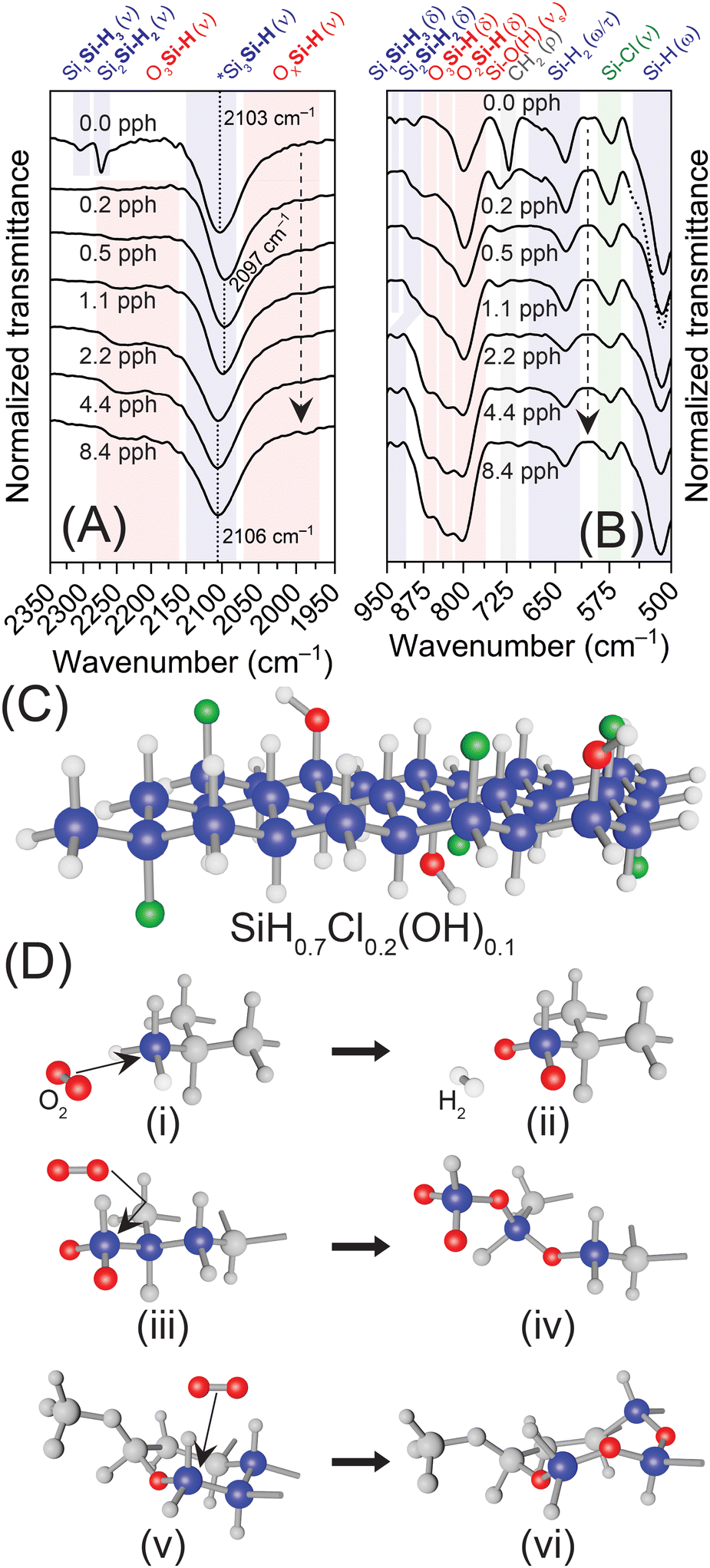 | ||
| Fig. 3 (A) and (B) FTIR spectra of SiNS samples exposed to increasing quantities of dried air; panel (A) highlights the changes to Si3–xSi–H1+x vibrations while panel (B) focuses on changes in Si–Hx bends and the Si–Cl vibration. The dashed arrows indicate increasing oxygen exposure. *Note, all FTIR spectra were normalized to the Si3Si–H stretch near 2100 cm−1. Also, the portion of the spectrum for the 0.2 pph O2:Si sample plotted as a dashed line in panel (B) is done so solely for clarity. (C) Structural schematic of SiNSs with nominally 70% hydrogen (white), 20% chlorine (green), and 10% hydroxyl (red & white) surface terminations (SiH0.7Cl0.2(OH)0.1). (D) Schematic of the proposed oxidation mechanism showing: (i) the initiating oxidative event via reaction of O2 with an SiH3 group forming (ii) O2SiH, (iii) oxidative attack of the formed O2Si group in (ii) leading to (iv) oxygen insertion into the Si backbone, and (v) and (vi) propagation of Si–O–Si and O2Si through the backbone with repeated oxygen exposure. Note: non-participating atoms in each step are grayed out for clarity. | ||
Optical and optoelectronic properties (PL, ΦPL)
We then characterized the SiNSs with steady-state photoluminescence spectroscopy, absolute ΦPL measurements, and time-resolved photoluminescence to elucidate the impact of the aforementioned chemical and structural changes on material properties. Most notably, the sample prepared in degassed HCl (0.0 pph O2:Si) displays completely different PL characteristics (spectral profile, peak position, ΦPL) than previously reported PL features for SiNSs (Fig. 2(C) and Fig. S12, ESI†).29,30,47 Specifically, this sample presents weak, broad PL centered near 610 nm with an absolute ΦPL as low as 0.2% (Fig. 2(C)), a full-width at half maximum (FWHM) of 160 nm, and a base width of 350 nm. The breadth of this peak indicates that this material possesses a broad distribution of states. The reproducibility of the PL is highlighted in Fig. S3(D) (ESI†). While minor differences in intensity are observed (ΦPL of 0.3–0.6%), a correlation between the extent of oxidation and ΦPL was not apparent at these low levels of oxidation. Thus, we attribute the differences in PL intensity to a combination of varying levels of (i) oxidation (undetectable by FTIR) and (ii) sample suspended in the excitation source; although standardized preparation protocols were employed, the poor dispersibility of these samples and their intense scattering nature lead to variability in solvent-based measurements. Conversely to the degassed HCl samples, when the SiNSs were prepared in air-saturated HCl (0.2 pph O2:Si), the PL intensity increased substantially (ΦPL ≈ 4–5%) and the peak maximum blueshifted to 520 nm (Fig. S12(A), ESI†). Additionally, exposure to this minute quantity of oxygen markedly decreased peak broadness (FWHM of 80 nm; 250 nm base width), indicating a reduction in distribution of states; similar spectral features were observed for other oxidized samples (Fig. S12(A), ESI†). Further increasing the quantity of oxygen exposure led to even higher PL intensity up to 1.1 pph O2:Si (ΦPL = 8.5%; Fig. 2(C)), after which the PL intensity decreased and blueshifted further. Specifically, for the highest O2:Si ratio tested (8.4 pph O2:Si), the PL peak maximum shifted to 516 nm and the absolute ΦPL decreased to 4.5% (Fig. 2(C)); this decrease is attributed to increasing SiO2 character.
To better understand these observations in the context of previous results, we compared the FTIR and steady-state PL spectra of the SiNSs prepared in degassed (0.0 pph O2:Si) and air-saturated (0.2 pph O2:Si) HCl to samples previously generated in our lab (Fig. S12(B) and S12(C), ESI†);29,30 the peak PL and FWHM values were extracted from all PL spectra and are provided in Fig. S12(D) (ESI†). These data show that the extent of oxidation varies greatly between these samples and the PL from previous samples is blueshifted relative to all samples explored in this work. While no clear trends emerged between the different samples, we do note the spectral shape of all the samples prepared in air-saturated HCl (0.2 pph O2:Si) is highly consistent. Despite this, the lack of correlations between the extent of apparent oxidation and peak PL for samples explored herein and previous samples suggests that there is another factor impacting PL that must be considered. One key difference between the samples in this work and our previous works is that the samples in the latter were washed with and dispersed in methanol (MeOH) for CaCl2 removal and characterization, respectively.29,30,45 Given that Si–halide groups can react with alcohols (R-OH) to produce Si-OR,58,59 we hypothesize that these differences are related to the formation of methoxy groups on the nanosheet surface.
We also characterized the SiNSs with room temperature time-correlated single photon counting and spectrally and time-resolved photoluminescence (Fig. S13, Tables S2, S3, ESI†). For all samples, the PL consists of a multicomponent decay with approximately 93% of the PL intensity decaying in under 30 ns, suggesting that the PL could arise from a direct bandgap transition. This rapid decay coupled with minimal contributions from the longer-lived component makes comparison of changes in direct vs. indirect character challenging. However, the general trends observed between the two measurements for increasing oxygen exposure are fairly consistent; the decay rate for the long-lived component first slows for slight oxygen exposure (1.1 pph O2:Si) but again increases upon further oxygen exposure (8.4 pph O2:Si). These trends suggest that increasing oxidation introduces more direct bandgap behavior, which is consistent with previous band structure simulations that demonstrated increasing oxidation (Si3SiH to O1Si2SiH to O3SiH; the bolded Si atoms are the central atom) shifted the band structure to direct.30 We conducted the time-correlated single photon counting measurements in both ACN and MeOH and the decays were fit to a tri-exponential function, for direct comparison to literature;29 the lifetimes and contributions for each component are provided in Table S2 (ESI†). For samples dispersed in ACN, clear trends emerge with increasing oxygen exposure: (i) the contributions from the fastest component (τ1) increase and (ii) the contributions for the two slower components (τ2 and τ3) both decrease. These trends coupled with the marked increase in ΦPL for the oxidized SiNSs relative to the 0.0 pph O2:Si sample suggests an increase in direct bandgap behavior. We note that, despite the observed increase in ΦPL, the ΦPL values are relatively low indicating the excited state depopulation is still dominated by non-radiative processes. Interestingly, the lifetimes for the sample prepared in degassed HCl (0.0 pph O2 : Si) are markedly shorter than all samples exposed to oxygen, which we tentatively attribute to the weaker PL from this sample at the wavelength monitored (510 nm; see Fig. 2(C)). Contrary to the ACN dispersions, a marked reduction in the lifetime of the third component occurred for MeOH-dispersed samples with increasing oxygen exposure, which suggests an increase in direct bandgap character, although the relatively consistent contributions do not support this. We note that the lifetime values and contributions for MeOH dispersions are consistent with those reported in literature;29 however, these values were for a sample with higher oxidization, based on the relative Si–O–Si vibration in FTIR (Fig. S12(B), ESI†). Further, this sample displayed a ΦPL of 9%, indicating that the photophysics are being influenced by yet another factor other than oxidation, such as the formation of methoxy (CH3O–) termination.
To better understand how the various components contribute to the spectral profile, we integrated the spectrally and time-resolved PL counts for select samples (0.0, 1.1, and 8.4 pph O2:Si) as a function of time range (Fig. S14, ESI†). For all samples, the decays are dominated by fast (<5 ns) but spectrally broad PL from 400 to nearly 800 nm, suggesting a broad distribution of direct states. For the 0.0 pph O2:Si sample (Fig. S14(A) and S14(B), ESI†), the PL peaks of the short-lived contributions are centered near 570 nm while the peaks of the weaker, longer-lived contributions (0.2–20 μs) are centered near 610 nm. For the 1.1 pph O2:Si sample (Fig. S14(C) and S14(D), ESI†), the PL peak of the short- and long-lived contributions are centered near 550 nm, while for the 8.4 pph O2:Si sample, the PL peak blueshifts further to approx. 520 nm (Fig. S14(E) and S14(F), ESI†). Additionally, the long-lived contributions for the 8.4 pph O2:Si sample essentially disappear, consistent with oxidation increasing direct bandgap character. These trends are also consistent with conclusions drawn from pXRD. That is, the outermost monolayers within a nanosheet stack and all edges/corners are oxidized first, leaving non-oxidized monolayers near the center of the stacks, which leads to, at minimum, a bimodal distribution of chemically distinct, photoluminescent materials; the parent SiH0.7Cl0.2(OH)0.1 and oxidized versions. Based on this, we tentatively attribute the long-lived PL observed on the far red-edge for the 0.0 pph O2:Si sample to radiative trap states (i.e., dangling bonds) that are passivated upon exposure to oxygen, as these features are not observed in samples exposed to dried air. These conclusions are further supported by the inset panel of Fig. S12(A) (ESI†), where the normalized steady-state PL for the 0.0, 0.2 1.1, and 8.4 pph O2:Si show (i) overlapping contributions centered near 510 nm which are attributed to oxidized nanosheets, (ii) overlapping contributions centered near 610 nm which are attributed to non-oxidized nanosheets, and (iii) an extended red-edge tail that is only present in the 0.0 pph O2:Si sample.
Although we fit the PL decays to triexponentials assuming a simple model of a direct radiative channel, a radiative trap state, and a non-radiative trap state, the true electronic structure model is much more complicated. As the above results show, the 2D Si consists of two chemically distinct populations; one very close to SiH0.7Cl0.2(OH)0.1 and another of variable oxidation, OxSiH0.7–yCl0.2–z(OH)0.1. Therefore, we tentatively attribute the fast and slow decay on the blue edge to bimolecular recombination and Shockley–Read–Hall (SRH) recombination, respectively, arising from oxidized nanosheets (OxSiH0.7–yCl0.2–z(OH)0.1), and the fast and the slow decay on the red edge to bimolecular recombination and SRH or surface recombination, respectively, in the non-oxidized nanosheets, SiH0.7Cl0.2(OH)0.1 As our previous report showed that nanosheets possess Si dangling bonds and these silyl radicals behave as midgap states,30 the decrease in the long-lived component on the red edge upon oxygen exposure and subsequent nanosheet oxidation indicates that oxygen has passivated these surface trap states. Therefore, oxidation results in two changes to the electronic structure: (i) the band structure switches from quasi-direct to direct, either due to chemical quantum confinement48–51 or conformational changes,60–62 and (ii) passivation of surface trap midgap states, both of which reduce the quantity of excited state relaxation through non-radiative channels. That said, as we only conducted room temperature measurements, concrete conclusions cannot be drawn about how the decay kinetics and previously simulated band structures correlate.
To reach a better understanding of these trends and contributions, we compared the experimentally observed PL peak wavelengths to simulated Eg's from our previous works (Fig. S15, ESI†).29,30,45 As we previously concluded that the surface termination of SiNSs prepared under conditions comparable to those reported herein is best represented by SiH0.7Cl0.2(OH)0.1 and previous DFT simulations suggest a direct bandgap with Eg of 1.68 eV (738 nm),45 the experimental observation of peak PL near 2.03 eV (610 nm) suggests an approximate 0.35 eV discrepancy between the simulated and experimental values. Indeed it is known that DFT underestimates Eg's.63,64 Operating under the assumption that this discrepancy remains constant for all samples, we adjusted our previously reported Eg's by 0.35 eV for the direct and indirect gaps of fully hydrogen-terminated SiNSs,29,30,45 as well as the direct gaps of the various oxidized structures.30 This adjustment revealed (i) that the experimentally observed PL peak for the oxidized samples (2.40 eV; 517 nm) lines up well with the predicted Eg for the previously studied structure with the highest oxidation, Si30H29(OH)1O3 (2.41 eV; 514 nm), suggesting that oxidation of the silicon backbone is occurring about Si–OH groups, and (ii) that oxidation of fully hydrogen-terminated SiNSs would slightly redshift the PL to approximately 515 nm (lowering of Eg), which is consistent with our previous band structure simulations.30
Proposed oxidative mechanisms
The oxidative source (i.e., O2vs. H2O) and associated mechanisms for the oxidation of hydrogen-terminated Si surfaces, such as Si(100) and Si(111), have been rigorously investigated,65–68 with literature suggesting that oxidation by molecular oxygen is initiated and propagated by radical reactions,66 that result in oxygen insertion between Si–Si bonds forming back-bonded siloxanes.66–68 Although bulk Si(111) surfaces often provide a robust model for comparison to SiNSs—indeed, the Si backbone of the monolayers possesses the same structure—such comparisons have their limitations, especially in relation to surface chemistry (reactions). That is, Si(111) surfaces are effectively of infinite thickness and contain very few SiH1+x groups, whereas SiNSs are monolayers with surface terminations on both sides and a plethora of SiH1+x groups along the periphery of the monolayers. Indeed, Chabal and coworkers demonstrated that the kinetics of oxidation were faster for a dihydride defect on a Si(111) surface over a defect-free, monohydride Si(111) surface.67 Therefore, we propose an oxidative mechanism based on increasing reactivity of SiHx towards oxygen; that is, SiH3 > SiH2 > SiH. In such a mechanism, the oxygen attacks the SiH3/SiH2 groups on the corners/edges of the SiNSs, liberating hydrogen and forming surface Si–O groups on the sheet periphery (not “bridged” surface siloxanes), followed by an inward propagation of oxidation towards the monolayer center (Fig. 3). Such a mechanism is supported by experimental results provided herein and our previous computational works.29,30,45 Note, the structures provided in Fig. 3 and Fig. S16 (ESI†) are not thermodynamically relaxed structures; the structures are simply schematic representations of the proposed surface termination and oxidative mechanisms. In the sample generated in degassed HCl (0.0 pph O2:Si), three peaks are observed for Si–H vibrations (Fig. 2(A), 3(A) and Fig. S3(B), ESI†) which are assigned to Si–H stretching of SiSi–H3, (2305 cm−1), Si2Si–H2 (2272 cm−1), and Si3Si–H (2100 cm−1). As oxygen exposure increased (i.e., air-saturated HCl (0.2 pph O2:Si)), the vibrations assigned to Si3–xSiH1+x disappear and the Si3Si–H vibration red-shifts due to increasing OxSiH vibrations (Fig. 3(A)). With further oxygen exposure, the peak then blue shifts due to the formation of O3SiH sites. The loss of SiH3 and SiH2 groups via hydrogen liberation and subsequent increase in OxSi sites is further supported by (i) the loss of the SiSi–H3 deformation mode at 932 cm−1, (ii) the decrease in SiH2 wagging/twisting between 500–750 cm−1, and (iii) the increase in Si–O–Si asymmetric stretching at 1050 cm−1 and OxSiH bending between 810–910 cm−1 (Fig. 3(B)). The symmetric stretching of Si–O observed around 800 cm−1 is attributed to both the Si–O present in Si–OH and Si–O formed on the sheet edges/corners upon initial stages of oxidation; the latter is evidenced by the slight increase in the intensity of this vibration with increasing oxygen exposure. Although this increase could be ascribed to insertion of oxygen in between Si–H to form Si–OH, the lack of an increasing stretch for Si–OH at approximately 3600 cm−1 with increasing oxidation indicates this does not occur. Furthermore, it is well established in the literature that oxygen atoms do not insert between Si and H to form Si–OH groups on hydrogen-terminated Si surfaces.66–68 Thus, the experimental evidence indicates that oxidation initiates along the sheet periphery through the reaction of molecular oxygen with SiH3 groups (Fig. 3(C) and 3(D)-i, ii); a similar reaction occurs with SiH2 edge groups once all SiH3 corner groups are oxidized (Fig. S16(A), ESI†). Oxidation then propagates inward through the formation of Si–O–Si “chains” via oxygen insertion into the Si network (i.e., “backbonding”), forming O2Si in the process (Fig. 3(D)-iii, vi). Given enough oxygen, O1Si and O2Si then oxidize to O3Si.
These conclusions are further supported by our previous DFT simulations.29,30,45 Our previous work predicted that bridging oxygens on the surface led to a shift in and broadening of the mode near 500 cm−1 due to emergence of additional vibrations between 500 and 600 cm−1, as well as between 700 and 800 cm−1, depending on which Si atoms are bridged (1–2 bridge vs. 1–3 bridge).30 Neither of these scenarios were observed experimentally in this work. Conversely, in our previous DFT simulations, oxygen inserted between Si bonds led to the emergence of multiple modes between 800–1100 cm−1, where the specific vibrations and relative intensities depend on (i) the quantity of oxygen inserted (1 to 3), (ii) the position inserted (about the same or neighboring Si atoms), and (iii) the geometric symmetry around the Si atoms (i.e., 3 inserted oxygen).30 Given the appearance and subsequent increase of modes at 830, 865, and 1030 cm−1 in the experimental data with no new modes appearing below 800 cm−1, our previous DFT simulations support oxidation of SiNSs arising from oxygen insertion and not surface bridging, a conclusion further supported by oxygen insertion being energetically favorable over the formation of surface siloxanes.30 Additionally, our previous DFT simulations predicted that it is enthalpically favorable to oxidize a Si atom bonded to at least one oxygen atom over an non-oxidized Si atom, supporting an oxidative propagation of Si–O–Si “chains” followed by subsequent oxidation to higher oxides (i.e., OxSi).
While the current evidence supports a mechanism based on SiHx reactivity, as the results also demonstrate a loss in chlorine termination (Fig. S7(D) and S10(A), ESI†), the reaction of oxygen with Si–Cl as an initiating event cannot be ruled out (Fig. S16(B), ESI†). Additionally, as our previous DFT simulations predicted that oxidation of OxSi is energetically favorable,30 the oxidation of Si atoms with hydroxyl termination as the initiating event also cannot be ruled out at this time (Fig. S16(C), ESI†). Indeed the aforementioned consistency in Eg (2.40 eV vs. 2.41 eV) between the intentionally oxidized samples and previously simulated oxidized nanosheets, Si30H29(OH)1O3,30 (2.40 eV vs. 2.41 eV; 514 nm), suggests that the Si–OH groups in the material are a key source for oxygen ingress into the backbone, with oxidation concentrating about Si–OH groups in the form of O3SiOH. Lastly, silyl radicals on the sheet edges/corners as the initiating event and propagating mechanism could also occur.66 Such a mechanism is supported by the loss of long-lived red PL observed in the PL measurements for oxidized samples. Further work is in progress to decouple these potential pathways and mechanistically understand the origin and propagation of oxidation through H-SiNSs.
Conclusions
We present a synthetic approach that yields hydrogen-terminated SiNSs with a structure that is closer to silicane than any previously reported (i.e., decreased siloxane content). These effectively non-oxidized SiNSs exhibit weak, broad PL centered near 610 nm with an absolute ΦPL as low as 0.2%, which is a marked deviation from the previously reported photoluminescence (500 nm; ΦPL = 9%). As our current synthetic protocols employ rigorously air-free preparations, the results clearly indicate that the minor oxidation (assessed by the appearance of Si–O(–Si) (a)symmetric stretching in FTIR) often observed for this material (i.e., silicane, siloxene, layered polysilane) mainly arises from dissolved oxygen in the aqueous HCl that is used during deintercalation of the CaSi2 precursor. Additionally, oxidation of the SiNS backbone is, in part, responsible for the commonly reported cyan (500 nm) PL. Indeed, the PL properties reported here for various levels of oxidized SiNSs explain the inconsistencies reported in the literature for SiNS PL; even in our own lab, we have observed the peak PL of freshly deintercalated SiNSs vary by as much as 30–40 nm (approximately 490 to 530 nm), which we attribute to varying degrees of oxidation that occurs when preparing samples.Furthermore, we show that exposure of the SiNSs to oxygen, leading to oxidation of the material, does not result in changes to the macroscopic structure but does impact the SiNS surface chemistry and backbone such that noteworthy changes in photoluminescence arise. Specifically, exposure to oxygen results in the loss of H-and Cl- terminal groups, the formation of OxSi networks, and passivation of dangling bonds. These chemical changes result in: (i) an increase the direct bandgap character of and (ii) a reduction in midgap states in 2D Si, evidenced by an increase in ΦPL and a shift in peak PL accompanied by a decrease in long-lived red emission. The trends observed in the PL are consistent with anticipated trends based on previous band structure simulations.30 Historically, this PL has been attributed to chemically quantum confined silicon via the formation of an extensive Si–O–Si networks;48–51 however, our experimental results here, combined with our previous band structure simulations, suggest that the buckling of the Si structure upon oxidation30 leads to a pseudo-conformation change from armchair- to boat-like that may increase the direct bandgap character.60–62 Lastly, our results reveal that oxidation provides an avenue for tuning bandgap in 2D Si, positioning this material ever closer to commercial application as the active layer in next-generation photonic and optoelectronic devices. However, as oxidation of the Si backbone does not fully account for previously observed PL properties, other strategies can be used to tune the bandgap (e.g., methoxy termination). Further work is underway to elucidate the exact structural composition of the non-oxidized SiNSs and decouple the PL contributions from oxidized and non-oxidized SiNSs (e.g., direct/indirect, methoxy termination).
Author contributions
Jeremy B. Essner: conceptualization, methodology, investigation, validation, data curation, formal analysis, visualisation, and writing – initial draft, review, and editing; Abhijit Bera: investigation, data curation, and writing – review and editing; Maharram Jabrayilov: investigation, data curation, and writing – review and editing; Abhishek Chaudhari: investigation, data curation, and writing – review and editing; Benjamin T. Diroll: resources, supervision, and writing – review and editing; Julia V. Zaikina: resources, supervision, and writing – review and editing; Matthew G. Panthani: funding, resources, conceptualization, project administration, supervision, visualization, and writing – initial draft, review, and editing.Data availability
Data for this article are available at Mendeley Data at https://data.mendeley.com/datasets/f3jcwz7tdj/1 (DOI: 10.17632/f3jcwz7tdj.1).Conflicts of interest
There are no conflicts to declare.Acknowledgements
The authors acknowledge the National Science Foundation (U.S.) Faculty Early CAREER Development Program (DMR-1847370) and DMR-2350483, which supported material synthesis and characterization. The authors would also like to acknowledge funding from the Air Force Office of Scientific Research under Award FA9550-20-10018, which supported the collection and analysis of ultrafast spectroscopy data. J. V. Z. acknowledges financial support from the National Science Foundation (U.S.) Division of Materials Research (DMR-1944551) CAREER Award. Work performed at the Center for Nanoscale Materials, a U.S. Department of Energy Office of Science User Facility, was supported by the U.S. DOE, Office of Basic Energy Sciences, under contract no. DE-AC02-06CH11357. Any opinions, findings, conclusions, or recommendations expressed in this material are those of the authors and do not necessarily reflect the views of the National Science Foundation.Notes and references
- M. Lundstrom, Science, 2003, 299, 210–211 CrossRef CAS PubMed.
- H.-S. P. Wong and S. Salahuddin, Nat. Nanotechnol., 2015, 10, 191–194 CrossRef CAS PubMed.
- M. Hochberg and T. Baehr-Jones, Nat. Photonics, 2010, 4, 492–494 CrossRef CAS.
- G. T. Reed, G. Mashanovich, F. Y. Gardes and D. J. Thomson, Nat. Photonics, 2010, 4, 518–526 CrossRef CAS.
- S. Z. Butler, S. M. Hollen, L. Cao, Y. Cui, J. A. Gupta, H. R. Gutiérrez, T. F. Heinz, S. Sae Hong, J. Huang, A. F. Ismach, E. Johnston-Halperin, M. Kuno, V. V. Plashnitsa, R. D. Robinson, R. S. Ruoff, S. Salahuddin, J. Shan, L. Shi, M. G. Spencer, M. Terrones, W. Windl and J. E. Goldberger, ACS Nano, 2013, 7, 2898–2926 CrossRef CAS PubMed.
- G. R. Bhimanapati, Z. Lin, V. Meunier, Y. Jung, J. Cha, S. Das, D. Xiao, Y. Son, M. S. Strano, V. R. Cooper, L. Liang, S. G. Louie, E. Ringe, W. Zhou, S. S. Kim, R. R. Naik, B. G. Sumpter, H. Terrones, F. Xia, Y. Wang, J. Zhu, D. Akinwande, N. Alem, J. A. Schuller, R. E. Schaak, M. Terrones and J. A. Robinson, ACS Nano, 2015, 9, 11509–11539 CrossRef CAS PubMed.
- Y. Meng, H. Zhong, Z. Xu, T. He, J. S. Kim, S. Han, S. Kim, S. Park, Y. Shen, M. Gong, Q. Xiao and S.-H. Bae, Nanoscale Horiz., 2023, 8, 1345–1365 RSC.
- P. Vishnoi, K. Pramoda and C. N. R. Rao, ChemNanoMat, 2019, 5, 1062–1091 CrossRef CAS.
- J. An, X. Zhao, Y. Zhang, M. Liu, J. Yuan, X. Sun, Z. Zhang, B. Wang, S. Li and D. Li, Adv. Funct. Mater., 2022, 32, 2110119 CrossRef CAS.
- Z. Cheng, R. Cao, K. Wei, Y. Yao, X. Liu, J. Kang, J. Dong, Z. Shi, H. Zhang and X. Zhang, Adv. Sci., 2021, 8, 2003834 CrossRef CAS.
- M. Ghosh Dastidar, I. Thekkooden, P. K. Nayak and V. Praveen Bhallamudi, Nanoscale, 2022, 14, 5289–5313 RSC.
- S. Al-Kabi, S. A. Ghetmiri, J. Margetis, T. Pham, Y. Zhou, W. Dou, B. Collier, R. Quinde, W. Du, A. Mosleh, J. Liu, G. Sun, R. A. Soref, J. Tolle, B. Li, M. Mortazavi, H. A. Naseem and S.-Q. Yu, Appl. Phys. Lett., 2016, 109, 171105 CrossRef.
- R. Soref, IEEE J. Sel. Top. Quantum Electron., 2006, 12, 1678–1687 CAS.
- R. Soref, Nat. Photonics, 2010, 4, 495–497 CrossRef CAS.
- D. Thomson, A. Zilkie, J. E. Bowers, T. Komljenovic, G. T. Reed, L. Vivien, D. Marris-Morini, E. Cassan, L. Virot, J.-M. Fédéli, J.-M. Hartmann, J. H. Schmid, D.-X. Xu, F. Boeuf, P. O’Brien, G. Z. Mashanovich and M. Nedeljkovic, J. Opt., 2016, 18, 73003 CrossRef.
- S. Shekhar, W. Bogaerts, L. Chrostowski, J. E. Bowers, M. Hochberg, R. Soref and B. J. Shastri, Nat. Commun., 2024, 15, 751 CrossRef CAS PubMed.
- M. Galbiati, N. Motta, M. De Crescenzi and L. Camilli, Appl. Phys. Rev., 2019, 6, 41310 Search PubMed.
- G. Shan, H. Tan, R. Ma, H. Zhao and W. Huang, Nanoscale, 2023, 15, 2982–2996 RSC.
- L. C. Lew Yan Voon, E. Sandberg, R. S. Aga and A. A. Farajian, Appl. Phys. Lett., 2010, 97, 163114 CrossRef.
- R. Soref, D. Buca and S.-Q. Yu, Opt. Photonics News, 2016, 27, 32–39 CrossRef.
- O. Olorunsola, A. Said, S. Ojo, H. Stanchu, G. Abernathy, S. Amoah, S. Saha, E. Wangila, J. Grant, S. Acharya, L. Miller, K. Rosler, Y. T. Jheng, G. E. Chang, B. Li, G. Salamo, S. Q. Yu and W. Du, J. Phys. D. Appl. Phys., 2022, 55, 443001 CrossRef CAS.
- D. Sciacca, M. Berthe, B. J. Ryan, N. Peric, D. Deresmes, L. Biadala, C. Boyaval, A. Addad, O. Lancry, R. Makarem, S. Legendre, D. Hocrelle, M. G. Panthani, G. Prévot, E. Lhuillier, P. Diener and B. Grandidier, Nanomaterials, 2022, 12, 1128 CrossRef CAS PubMed.
- C. Livache, B. J. Ryan, U. Ramesh, V. Steinmetz, C. Gréboval, A. Chu, T. Brule, S. Ithurria, G. Prévot, T. Barisien, A. Ouerghi, M. G. Panthani and E. Lhuillier, Appl. Phys. Lett., 2019, 115, 52106 CrossRef.
- B. J. Ryan, B. T. Diroll, Y. Guo, C. J. Dolgos, Q. H. Wang, L. T. Roling and M. G. Panthani, ECS Trans., 2021, 102, 3 CrossRef CAS.
- M. S. Ferris, A. P. Chesney, B. J. Ryan, U. Ramesh, M. G. Panthani and K. J. Cash, Sens. Actuators, B, 2021, 331, 129350 CrossRef CAS.
- S. Ng and M. Pumera, Adv. Mater., 2023, 35, 2207196 CrossRef CAS.
- S. Jiang, M. Q. Arguilla, N. D. Cultrara and J. E. Goldberger, Acc. Chem. Res., 2015, 48, 144–151 CrossRef CAS.
- W. L. B. Huey and J. E. Goldberger, Chem. Soc. Rev., 2018, 47, 6201–6223 RSC.
- B. J. Ryan, M. P. Hanrahan, Y. Wang, U. Ramesh, C. K. A. Nyamekye, R. D. Nelson, Z. Liu, C. Huang, B. Whitehead, J. Wang, L. T. Roling, E. A. Smith, A. J. Rossini and M. G. Panthani, Chem. Mater., 2020, 32, 795–804 CrossRef CAS.
- B. J. Ryan, L. T. Roling and M. G. Panthani, ACS Nano, 2021, 15, 14557–14569 CrossRef CAS.
- S. W. Kim, J. Lee, J. H. Sung, D. Seo, I. Kim, M.-H. Jo, B. W. Kwon, W. K. Choi and H.-J. Choi, ACS Nano, 2014, 8, 6556–6562 CrossRef CAS.
- N. D. Drummond, V. Zólyomi and V. I. Fal’ko, Phys. Rev. B: Condens. Matter Mater. Phys., 2012, 85, 75423 CrossRef.
- A. Stathis, M. Stavrou, I. Papadakis, J. Mock, M. J. Kloberg, M. Becherer, A. Lyuleeva-Husemann and S. Couris, J. Phys. Chem. C, 2021, 125, 18510–18516 CrossRef CAS.
- H. Imagawa and H. Itahara, Dalton Trans., 2017, 46, 3655–3660 RSC.
- R. Gao, J. Tang, X. Yu, S. Lin, K. Zhang and L.-C. Qin, Adv. Funct. Mater., 2020, 30, 2002200 CrossRef CAS.
- C. Wang, X. Xu, X. Pi, M. D. Butala, W. Huang, L. Yin, W. Peng, M. Ali, S. C. Bodepudi, X. Qiao, Y. Xu, W. Sun and D. Yang, Nat. Commun., 2022, 13, 5216 CrossRef CAS.
- Y. You, C. Yang, X. Zhang, H. Lin and J. Shi, Mater. Today Nano, 2021, 16, 100132 CrossRef CAS.
- F. Wöhler, Justus Liebigs Ann. Chem., 1863, 127, 257–274 CrossRef.
- H. Kautsky, Z. Anorg. Allg. Chem., 1921, 117, 209–242 CrossRef.
- H. Kautsky and G. Herzberg, Z. Anorg. Chem., 1924, 139, 135–160 CrossRef CAS.
- A. Weiss, G. Beil and H. Meyer, Z. Naturforsch., B, 1980, 35, 25–30 CrossRef.
- J. R. Dahn, B. M. Way, E. Fuller and J. S. Tse, Phys. Rev. B: Condens. Matter Mater. Phys., 1993, 48, 17872–17877 CrossRef CAS PubMed.
- S. Yamanaka, H. Matsu-ura and M. Ishikawa, Mater. Res. Bull., 1996, 31, 307–316 CrossRef CAS.
- K. Nishimura, Y. Nagao, S. Yamanaka and H. Matsu-ura, Jpn. J. Appl. Phys., 1996, 35, L293 CrossRef CAS.
- R. W. Dorn, B. J. Ryan, S. N. S. Lamahewage, M. V. Dodson, J. B. Essner, R. Biswas, M. G. Panthani and A. J. Rossini, Chem. Mater., 2023, 35, 539–548 CrossRef CAS.
- X. Deng, X. Zheng, T. Yuan, W. Sui, Y. Xie, O. Voznyy, Y. Wang and Z. Yang, Chem. Mater., 2021, 33, 9357–9365 CrossRef CAS.
- D. Karar, N. Ratan Bandyopadhyay, A. Kumar Pramanick, D. Acharyya, G. Conibeer, N. Banerjee, O. E. Kusmartseva and M. Ray, J. Phys. Chem. C, 2018, 122, 18912–18921 CrossRef CAS.
- M. S. Brandt, H. D. Fuchs, M. Stutzmann, J. Weber and M. Cardona, Solid State Commun., 1992, 81, 307–312 CrossRef CAS.
- P. Deák, M. Rosenbauer, M. Stutzmann, J. Weber and M. S. Brandt, Phys. Rev. Lett., 1992, 69, 2531–2534 CrossRef.
- H. D. Fuchs, M. Stutzmann, M. S. Brandt, M. Rosenbauer, J. Weber and M. Cardona, Phys. Scr., 1992, 1992, 309 CrossRef.
- M. Stutzmann, M. S. Brandt, M. Rosenbauer, J. Weber and H. D. Fuchs, Phys. Rev. B: Condens. Matter Mater. Phys., 1993, 47, 4806–4809 CrossRef CAS PubMed.
- B. J. Ryan, G. Bhaskar, J. B. Essner, A. Bera, R. W. Dorn, Y. Guo, Q. Hua Wang, A. J. Rossini, J. V. Zaikina, L. T. Roling and M. G. Panthani, ACS Appl. Nano Mater., 2023, 6, 10054–10063 CrossRef CAS.
- S. Rivillon, F. Amy, Y. J. Chabal and M. M. Frank, Appl. Phys. Lett., 2004, 85, 2583–2585 CrossRef CAS.
- B. J. Eves and G. P. Lopinski, Surf. Sci., 2005, 579, 89–96 CrossRef.
- F. A. Soria, E. M. Patrito and P. Paredes-Olivera, J. Phys. Chem. C, 2013, 117, 18021–18030 CrossRef CAS.
- M. F. Juarez, E. M. Patrito and P. Paredes-Olivera, J. Phys. Chem. C, 2008, 113, 681–690 CrossRef.
- G. Allen Ferguson, S. Rivillon, Y. Chabal and K. Raghavachari, J. Phys. Chem. C, 2009, 113, 21713–21720 CrossRef.
- R. Wakabayashi, Y. Sugiura, T. Shibue and K. Kuroda, Angew. Chem., Int. Ed., 2011, 50, 10708–10711 CrossRef CAS.
- N. Jingu, K. Sumida, T. Hayakawa, T. Ono and K. Saitow, Chem. Mater., 2024, 36, 5077–5091 CrossRef CAS.
- P. Zhang, X. D. Li, C. H. Hu, S. Q. Wu and Z. Z. Zhu, Phys. Lett. A, 2012, 376, 1230–1233 CrossRef CAS.
- M. Houssa, E. Scalise, K. Sankaran, G. Pourtois, V. V. Afanas’ev and A. Stesmans, Appl. Phys. Lett., 2011, 98, 223107 CrossRef.
- Y. Ding and Y. Wang, J. Phys. Chem. C, 2018, 122, 23208–23216 CrossRef CAS.
- P. Miró, M. Audiffred and T. Heine, Chem. Soc. Rev., 2014, 43, 6537–6554 RSC.
- Á. Morales-García, R. Valero and F. Illas, J. Phys. Chem. C, 2017, 121, 18862–18866 CrossRef.
- Y. J. Chabal and L. C. Feldman, Electrochem. Soc. Interface, 2005, 14, 31 CrossRef CAS.
- F. A. Soria, E. M. Patrito and P. Paredes-Olivera, J. Phys. Chem. C, 2012, 116, 24607–24615 CrossRef CAS.
- X. Zhang, Y. J. Chabal, S. B. Christman, E. E. Chaban and E. Garfunkel, J. Vac. Sci. Technol., A, 2001, 19, 1725–1729 CrossRef CAS.
- B. Gokce, E. J. Adles, D. E. Aspnes and K. Gundogdu, Proc. Natl. Acad. Sci. U. S. A., 2010, 107, 17503–17508 CrossRef CAS.
Footnote |
| † Electronic supplementary information (ESI) available: Experimental details, pXRD, SEM images, EDS analyses, FTIR, PL, TRPL. See DOI: https://doi.org/10.1039/d4nh00387j |
| This journal is © The Royal Society of Chemistry 2025 |