
Engineering energy bands in 0D–2D hybrid photodetectors: Cu-doped InP quantum dots on a type-III SnSe2/MoTe2 heterojunction†
Jiabin Li‡
a,
Dongxue Wang‡a,
Xiya Chena,
Yao Zhoua,
Huanteng Luoa,
Tu Zhaoa,
Sheng Hua,
Zhaoqiang Zheng b,
Wei Gao*a and
Xiao Liu*a
b,
Wei Gao*a and
Xiao Liu*a
aGuangdong Provincial Key Laboratory of Chip and Integration Technology, School of Electronic Science and Engineering (School of Microelectronics), Faculty of Engineering, South China Normal University, Foshan 528200, P. R. China. E-mail: gaowei317040@m.scnu.edu.cn; liuxiao@m.scnu.edu.cn
bCollege of Materials and Energy, Guangdong University of Technology, Guangzhou 510006, P. R. China
First published on 14th February 2025
Abstract
Two-dimensional (2D) self-driven photodetectors have emerged as a compelling area of research, offering advantages such as miniaturization, weak light detection, high photosensitivity, and low noise levels. However, current type-III 2D heterojunction photodetectors often suffer from low self-driven responsivity and medium Ilight/Idark ratios. In this work, a novel device architecture that addresses these challenges is constructed by incorporating Cu-doped InP/ZnSeS/ZnS core–shell quantum dots (QDs) onto a type-III SnSe2/MoTe2 2D heterojunction. The strategically engineered energy band structure of the Cu-doped QDs facilitates carrier transport with SnSe2/MoTe2 to form back-to-back type-II and type-III band alignments. As a result, under 532 nm illumination, the hybrid device exhibits remarkable visible light self-driven performance metrics with the help of the photogating effect: an ultra-low dark current of 23 fA, with responsivity and external quantum efficiency enhanced to 459 mA W−1 and 109%, respectively, surpassing theoretical values by fourfold compared to those of pure SnSe2/MoTe2, a low noise equivalent power (NEP) of 0.87 × 10⁻² pW Hz−1/2, a realistic specific detectivity of 1.45 × 10¹¹ Jones, a large Ilight/Idark ratio of 106 and a swift response time of 1.16 ms/1.14 ms with stable operation. These results demonstrate that energy band engineering of Cu-doped QDs can significantly enhance the performance of 2D type-III heterojunctions in the visible range, laying a foundation for future gate-tunable optoelectronic devices.
New conceptsThis study introduces a novel concept of integrating Cu-doped InP/ZnSeS/ZnS quantum dots (QDs) with type-III SnSe2/MoTe2 van der Waals heterostructures to enhance the performance of 2D photodetectors in the visible region. This concept is distinguished from existing research by its strategic energy band engineering and the use of Cu doping to optimize the photovoltaic performance of QDs. This work brings additional insights to nanoscience and nanotechnology by demonstrating that doping can significantly improve the visible light response and overall performance of 2D type-III heterojunction photodetectors. It shows that by engineering the energy band structure and optimizing the valence and spatial arrangement of doped metal cations, the charge transfer efficiency can be enhanced, leading to improved photovoltaic performance. This approach not only addresses the challenges related to carrier transport and stability in QDs but also opens new avenues for tailored QD synthesis, offering a path to develop environmentally friendly, high-performance optoelectronic devices. |
Introduction
Photodetectors play a pivotal role in modern technology, with applications in high-speed optical fiber communication, image sensors, artificial visual perception systems, multicolored imaging systems and autonomous vehicles.1–3 Two-dimensional (2D) materials without surface dangling bonds, stacked via van der Waals forces, offer robust light–matter interactions without the constraints of lattice matching. Thus, the design of van der Waals heterostructures (vdWHs) has emerged as a hot topic and 2D vdWH photodetectors hold immense promise for next-generation optoelectronics.4 In general, semiconductor heterojunctions exhibit three primary energy band configurations: straddling gap (type-I),5,6 staggered gap (type-II)7–9 and broken gap (type-III).10–14 Type-III band alignment spatially separates electrons and holes within the individual components at zero bias. The large band offset enables low dark currents through the direct tunneling effect. Under the built-in electric field, photogenerated carriers readily return to their respective electrodes without overcoming the potential barriers across each electron depletion or accumulation region, thereby reducing the probability of electron–hole recombination and shortening the response time.15,16 However, the self-driven responsivity (R) of most type-III photodetectors is likely poor without an effective generation and separation process throughout the entire depletion region across the interface instead of the depletion region in type-II band alignment. Recent years have witnessed the emergence of 2D type-II photodetectors based on WSe2/GaSe,17 p-GaSe/n-InSe,18 p-BP/n-ReS219 and GaSe/WS220 vdWHs, as well as type-III photodetectors based on black phosphorus BP/ReS2,21 GeSe/SnS2,22 WSe2/SnS223 and MoTe2/SnSe224–27 vdWHs. In the case of SnSe2/MoTe2, previous studies have primarily focused on its excellent performance in the infrared light range, particularly at 808 nm, while its performance in the visible range has not been thoroughly investigated. Most of these type-III photodetectors still face challenges in achieving comprehensive photovoltaic performance, especially in simultaneously attaining high R and fast response speed in the visible region. Fortunately, energy band engineering presents a promising solution by incorporating additional band arrangements to construct double heterojunctions, which can enhance photocurrent generation and separation processes, thereby improving key performance parameters. Regarding all-2D double heterojunctions,28–32 Ma et al. designed a SnSe2/Bi2Se3/MoTe2 double heterostructure with back-to-back type-III band alignment. Compared to MoTe2/SnSe2, the R increased from 13 to 492.8 mA W−1 and the EQE increased from 2% to 76% at a gate voltage of 60 V under 808 nm illumination.29 However, studies on 0D/2D double heterojunctions are very limited, highlighting the need for developing a universal and facile strategy to enhance the photovoltaic performance of SnSe2/MoTe2 in the visible region.Hopefully, colloidal quantum dots (QDs) have emerged as versatile building blocks for innovative photodetectors, owing to their high absorption coefficients in the visible range, tunable bandgaps, and solution processability.33,34 Based on this, numerous studies have investigated 0D/2D hybrid photodetectors by leveraging the light absorption and charge separation efficiency of QDs.33–35 As for 0D/2D hybrid photodetectors with individual 2D channels, the enhanced R can be ascribed to the photoconductive and photogating effects observed in devices such as FAPbBr3 QDs/graphene,36 CsPbI3−xBrx QDs/MoS2,37 CdSe@Zn1−xCdxS QDs/InSe,38 and so on. However, these configurations also exhibit significant drawbacks, including high dark current, poor response times and low Ilight/Idark ratio. While developing a 0D/2D hybrid photodetector featuring a 2D heterojunction channel, Zeng et al. recently designed a PbS QDs/MoS2/WSe2 vdWH photodiode with a back-to-back type-II band alignment. This design resulted in a slight enhancement of the self-driven responsivity, increasing from 426 mA W−1 to 760 mA W−1 when compared to MoS2/WSe2 under 756 nm illumination.39 Wang et al. designed PbS QD/MoS2/BP dual-band infrared photodetectors that operate at room temperature. The spin-coating of PbS QDs enables a bias-selectable photoresponse in both photodiode and phototransistor modes. In the photodiode mode, it exhibits a high D* value of 5 × 10⁹ Jones at a λ value of 2.2 μm.40 Above all, it is evident that the carrier transport in the 2D heterojunction can be effectively regulated through energy band engineering by introducing a QD layer with high absorption in a specific wavelength range. Nevertheless, while the optimal response range and optoelectronic performance of type-II photodetectors can be improved by incorporating QDs, there remains significant potential to improve the visible photoresponse behavior of 2D type-III heterojunction photodetectors through QD modification via band engineering to trade off the relationship between R and the response speed.
Given the environmental concerns surrounding heavy metals (Cd, Pb, and Hg) in electronics, InP QDs have emerged as an eco-friendly alternative with tunable absorption spectra in the visible region.41,42 To address surface defects and non-radiative recombination in conventional InP QDs, core–shell structures have been developed. ZnS shell materials effectively confine carriers to InP cores, but the 7.7% lattice mismatch between InP and ZnS can induce interfacial strain.43,44 Therefore, intermediate shell layers with moderate lattice constants, such as ZnSe,45 ZnSeS,46 and GaP,47 are introduced to mitigate interfacial defects and enhance photoresponse performance. Despite these advancements, InP/ZnSeS/ZnS quantum dots still encounter challenges related to carrier transport and stability. Elemental doping provides a pathway to further improve the performance of QDs.48 By optimizing the valence and spatial arrangement of the doped metal cations, the charge transfer efficiency can be enhanced, leading to improved photovoltaic performance.49,50 The impact of different metal cation dopants on the properties of QDs opens new avenues for tailored QD synthesis.51–53
In this study, we present a 0D/2D hybrid photodetector comprising type-III SnSe2/MoTe2 vdWHs coupled with Cu-doped InP/ZnSeS/ZnS QDs, namely InP QDs, which serve as the photosensitive layer. In depth, Cu doping modifies the energy band structure of the InP QDs, introducing Cu correlation states that accelerate the transfer of photogenerated carriers and optimize photovoltaic performance.50,54 After spin-coating the InP QDs onto the SnSe2/MoTe2 heterojunction, we observe a significant increase in the absorption coefficient of the hybrid structure across the wavelength range of 330 nm to 770 nm. The positive photocurrent is concentrated in the overlapping region near the edge of the SnSe2/MoTe2 interface at zero bias under 520 nm illumination, as indicated by the scanning photocurrent mapping (SPCM). By leveraging back-to-back type-II and type-III band alignments, the photogenerated holes on the SnSe2 side can be effectively boosted and collected to the electrode by the accumulation of holes at the QDs. Compared to SnSe2/MoTe2, the R significantly increases from 112 mA W−1 to 459 mA W−1, and the Ilight/Idark ratio enhances from 103 to 106 in the hybrid photodetector. The device also achieves a high EQE of 109% (>100%), a high D* value of 1.45 × 10¹¹ Jones and a rapid response time of 1.16/1.14 ms. This work provides a novel and facile approach for developing environmentally friendly, high photovoltaic performance InP QDs/2D hybrid photodetectors based on the type-III 2D heterojunction in the visible region.
Results and discussion
The synthetic pathway illustrated in Fig. 1(a) depicts the fabrication of InP QDs through a thermal injection method, with modifications based on previously reported procedures.45,54 Fig. 1(b) demonstrates that the synthesized InP QDs exhibit a nearly monodisperse size distribution, with an average diameter of 2.6 ± 0.33 nm. The inset and Fig. S1 (ESI†) show the corresponding high-resolution transmission electron microscopy (HRTEM) images, and the averaged interplanar spacing of the six lattices is approximately 0.34 nm, corresponding to the (111) plane of the zinc blende structure of InP QDs.55 Elemental mapping via energy dispersive X-ray spectroscopy (EDS), as presented in Fig. S2 (ESI†), confirms the well-dispersed and relatively uniform particle size of the InP QDs. The uniform distribution of copper elements suggests successful doping within the quantum dots. Subsequently, we investigated the optical properties of the InP QDs using steady-state absorption and photoluminescence (PL) spectra (Fig. 1(c)). Compared with the PL spectra before Cu doping (Fig. S3, ESI†), Fig. 1(c) reveals a redshift of 49 nm from the original peak at 515 nm, along with the emergence of an additional PL peak at 633 nm in the Cu-doped QDs. This indicates the formation of a distinct energy level near the valence band maximum (Ev) due to Cu doping.49,56 The inset displays the Tauc plot of the sample, from which the optical bandgap (Eg) of the Cu-doped InP QDs was determined to be 2.77 eV. Another inset image shows the physical appearance of the InP QDs under natural light and a 365 nm UV lamp. Fig. 1(d) presents the valence band X-ray photoelectron spectroscopy (VB-XPS) spectrum of the InP QDs. The Ev was calculated to be −5.86 eV and the Fermi level (Ef) was determined to be −4.56 eV.57 Consequently, the conduction band minimum (Ec) is determined to be −3.09 eV (The calculation method is detailed in Note S1, ESI†). The Cu-doped InP QDs exhibit two emission peaks due to Cu doping, with the 633 nm peak appearing after Cu doping. According to the previous reports,58,59 the doped Cu energy levels (ECu) are relatively close to the valence band, and the energy difference between the ECu and the Ec is estimated to be 1.96 eV by 1240/λ, indicating that ECu is located at −5.05 eV (the calculation method is detailed in Note S1, ESI†). Finally, the band structure diagram of InP QDs (shown in the inset of Fig. 1(d)) can be utilized for further analysis of the charge transport mechanisms and band alignment bending. The optical properties and band structures of InP (No-doped) QDs are shown in Fig. S4 (ESI†). These results suggest that the doping of Cu can effectively tune the band structure and the doping type to design an appropriate band alignment with type-III heterostructure, enhancing the optoelectrical performance of photodetectors.57–59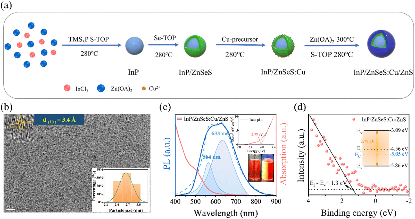 | ||
| Fig. 1 (a) Synthesis of InP/ZnSeS:Cu/ZnS QDs. (b) TEM image of InP/ZnSeS:Cu/ZnS QDs with the size-distribution histogram (bottom-right) and the lattice interplanar spacing (top-left). (c) Absorption (pink lines) and photoluminescence (blue lines) spectra of InP/ZnSeS:Cu/ZnS QDs. The inset shows the converted Kubelka–Munk functions in relation to their photon energy and a physical diagram under a 365 nm UV lamp and natural light. (d) The band structure of InP/ZnSeS:Cu/ZnS QD alignments estimated based on the UV-Vis absorption spectra and VB-XPS data. The inset shows the energy band diagram. | ||
Firstly, a series of SnSe2/MoTe2 heterojunction devices are fabricated using mechanical tape stripping and the PDMS dry transfer method, with the final devices achieved through the spin-coating of InP QDs. The device structure diagram of the InP/SnSe2/MoTe2 heterojunction is presented in Fig. 2(a). A 10 nm Cr/50 nm Au metal was selected for connection to the exfoliated MoTe2 and SnSe2, where the bottom MoTe2 serves as the drain terminal and the top SnSe2 functions as the source terminal. Notably, the InP QDs act as a top photosensitive layer. A detailed description of the fabrication process can be found in the experimental section. Fig. 2(b) shows the corresponding optical microscopy image, revealing that the overlapped area of SnSe2/MoTe2 device I was calculated to be 67 μm2. In comparison to the optical microscopy image of SnSe2/MoTe2 device I illustrated in Fig. S5 (ESI†), InP QDs have been successfully spin-coated onto the prepared heterostructure photodetector. To further investigate the vibrational modes of individual components and the layer coupling effect in the InP QDs/SnSe2/MoTe2 heterostructure, Raman spectroscopy was conducted, as shown in Fig. 2(c). Firstly, two characteristic peaks were observed at 171 cm−1 and 231 cm−1 for the individual multilayered 2H-MoTe2, while 1T-SnSe2 exhibited a characteristic peak located at 183 cm−1. In the case of the SnSe2/MoTe2 heterostructure, all Raman peaks were obtained without any shift. Nevertheless, the Raman quenching of MoTe2 is attributed to the strong coupling effect at the SnSe2/MoTe2 interface. Notably, for InP/SnSe2/MoTe2, the A1g peak of MoTe2 displayed a significant redshift of 12 cm−1, while the E12g peak showed a prominent blueshift of 26 cm−1. The Raman spectra of InP/MoTe2 also exhibited redshifts and blueshifts in Fig. S6 (ESI†). It indicates that the spin coating of InP QDs induces both electron and hole doping, with hole doping being more pronounced.60,61 Fig. S7 (ESI†) shows the absorption spectra of SnSe2/MoTe2 and InP/SnSe2/MoTe2 within the wavelength range of 250–1000 nm. It is evident that the absorption coefficient of the InP/SnSe2/MoTe2 heterojunction surpasses that of SnSe2/MoTe2, particularly in the range of 330–770 nm. The optimal absorption coefficient is observed in the range of 400–500 nm. Atomic force microscopy (AFM) was employed to measure the thicknesses of MoTe2 and SnSe2 in device I. The corresponding AFM image presented the height profiles of MoTe2 and SnSe2 along the green and blue lines (Fig. S8, ESI†), indicating a smooth and clean surface of the heterojunction, free of bubbles. Fig. 2(d) presents that the thicknesses of the bottom MoTe2 and top SnSe2 are measured to be approximately 20 nm and 30 nm, respectively. The surface potential difference (SPD) at the SnSe2/MoTe2 interface is determined through Kelvin probe force microscopy (KPFM) measurements. As depicted in Fig. 2(e), the average SPDs of the individual SnSe2 and MoTe2 surfaces can be measured and calculated (the calculation method is detailed in Note S2, ESI†). The ΔEf values are calculated to be 25 meV and the built-in electric field points from MoTe2 to SnSe2. According to the previous reports,24 the theoretical Ec and Ev values for the multilayered MoTe2 and SnSe2 are 3.9 eV/4.92 eV and 5.3 eV/6.37 eV, respectively. Simultaneously, the theoretical Eg values of multilayered MoTe2 and SnSe2 are 1.02 eV and 1.07 eV, respectively. To confirm the polar conduction characteristics of individual MoTe2 and SnSe2 at similar thicknesses, the corresponding transfer curves are presented in Fig. S9 (ESI†). The results indicate that multilayered SnSe2 exhibits poor gate-modulation ability due to heavy n-type doping, which reflects the degenerate nature of multilayered SnSe2.62 The Ef of SnSe2 can be estimated to be situated beyond Ec. In contrast, the exfoliated MoTe2 demonstrates a p-type conducting behavior, with a hole Ion/Ioff ratio of 1.5 × 10³. Moreover, the p-type threshold voltage is determined to be −33 V by linear extrapolation.63 Fig. 2(f) illustrates the band alignment of the InP/n-SnSe2/p-MoTe2 heterostructure before contact. As for the InP QDs/top SnSe2 interface, the conduction band offset (ΔEc) and the valence band offset (ΔEv) between InP QDs and SnSe2 were calculated to be 2.21 eV and 0.51 eV, respectively. A type-II band alignment is established across the InP QDs/SnSe2 interface. The Ef value of InP QDs is higher than that of SnSe2, leading to the formation of a built-in electric field (Vbi-1) directed from InP QDs to SnSe2. For the traditional type-III SnSe2/MoTe2 interface, the tunneling window between the Ev of MoTe2 and the Ec of SnSe2 was measured to be 0.38 eV. It is known that the EF of MoTe2 is higher than that of SnSe2, suggesting that another built-in electric field (Vbi-2) can be generated at the SnSe2/MoTe2 interface. Consequently, the back-to-back type-II and type-III band alignment of our designed double heterostructure has been verified. After contact, as shown in Fig. S10 (ESI†), to reach the thermal equilibrium, the electrons at the Ef of InP QDs diffuse to that of SnSe2, resulting in the formation of positive charge centers at the band edge of the InP QDs. Consequently, the band edge of the InP QDs bends significantly upwards. In contrast, the band edge of the degenerated SnSe2 exhibits a slight downward bend. The depletion region of electrons is primarily located on the InP QD side, which has lower conductivity. Simultaneously, minority electrons from MoTe2 can diffuse into SnSe2, facilitating a more pronounced upward band bending towards the SnSe2 edge. While the band edge of SnSe2 slightly bends downwards. As a result, electrons diffuse from MoTe2 to SnSe2, leading to electron accumulation at the SnSe2 interface. We forecast that the additional type-II band alignment of InP QDs/SnSe2 will boost the number of photogenerated holes in the type-III SnSe2/MoTe2 heterostructure, thereby enhancing the photovoltaic performance.
 | ||
| Fig. 2 (a) Device structure diagram of InP/SnSe2/MoTe2. (b) Optical microscopy image of InP/SnSe2/MoTe2 device I. (c) Raman spectra of MoTe2, SnSe2, SnSe2/MoTe2, and InP/SnSe2/MoTe2 heterojunctions. (d) Height profiles of MoTe2 and SnSe2. (e) KPFM image and surface potential difference profile of the heterojunction along the pink lines. (f) Energy band diagram of the InP/SnSe2/MoTe2 heterostructure prior to contact. | ||
To highlight the effect of lnP QDs on the improved photovoltaic performance of the SnSe2/MoTe2 heterostructure photodetector, we compare and analyze the photoresponse behavior of the SnSe2/MoTe2 heterostructure before and after the spin coating of InP QDs for device I under 532 nm illumination. Fig. 3(a) presents the Ids–Vds curves of the InP/SnSe2/MoTe2 both under dark conditions and at various incident light power densities (P). The double heterostructure shows backward rectifying behavior, with a low backward rectification ratio of 7. Notably, the illuminated Ids increases at both positive and negative Vds as the P increases, demonstrating the photoconductive effect. In particular, several distinct values of positive short-circuit current (Isc) and negative open-circuit voltage (Voc) are observed, attributed to the photovoltaic effect. The corresponding band alignment at Vds = 0.3 V and 0 V will be discussed later. Fig. 3(b) displays the corresponding time-resolved photoresponse curves at varying light power densities. The fabricated photodetector demonstrates fast and reproducible photo-switching on–off characteristics. The light current (Ilight) increases monotonously with the increase in P and exhibits a stable on-state. The dark current (Idark) is suppressed within the range of 23 fA to 78 fA, which can be attributed to the effective double carriers’ depletion regions in the InP QDs/SnSe2/MoTe2 heterojunction.64 The dark current mentioned here refers to the current that persists after the pulsed laser is turned off at a specific light power density, which can be extracted to investigate the recombination rate and reproducibility of the photodiode at zero bias. It is noteworthy that all of our fabricated devices exhibit a slightly fluctuating dark current that is less than one order of magnitude, independent of the light illumination. In contrast, the Idark value of the SnSe2/MoTe2 heterojunction is approximately 2 pA, as shown in Fig. S11 (ESI†). Furthermore, the extracted negative Voc and positive Isc as a function of P are illustrated in Fig. 3(c). Both Voc and Isc increase to their maximum values of 0.16 V and 56.66 nA at P = 181.44 mW cm−2. Generally, the linear relationship between Isc and P can be described by Isc ∝ Pα. After linear fitting, the exponent factor (α) was determined to be 1.79 (α > 1), while the α value of 1.75 for the SnSe2/MoTe2 photodetector was lower but still greater than 1, as shown in Fig. S12 (ESI†). These super-linear behaviors have not been reported or discussed in previous studies of SnSe2/MoTe2 photodetectors. First, our selected type-III heterostructure effectively inhibits the probability of nonradiative recombination along the interlayer direction, allowing photogenerated electrons and holes to return to the electrodes without the need for interfacial transport. Second, at higher incident power levels, the recombination centers located in the mid-gap of the intralayer of SnSe2 and MoTe2 can be easily occupied, leading to the closure of the recombination channel for the narrow band gaps of MoTe2 and SnSe2. Thus, the reduced recombination rate at elevated intensities facilitates greater optoelectrical efficiency and contributes to the super-linear behavior observed in power dependence.65 The Pel generated by the photodetector at various P values is illustrated in Fig. 3(d). The maximum Pel reaches 1.09 nW and 1.82 nW for device I. Furthermore, considering that photoelectric conversion efficiency (PCE) and fill factor (FF) are critical quality factors for photovoltaic devices, as shown in Fig. S13 (ESI†) (the calculation method is detailed in Note S3, ESI†), the corresponding maximum PCE and FF values for device I are 0.14%/0.9% and 0.41%/1.5%, respectively. This indicates that our designed hybrid vdWH demonstrates enhanced photoelectric efficiency due to the hole injection from the InP QD layer. To figure out the photocurrent distribution to analyze the charge transport process via band alignment, the SPCM of the InP/SnSe2/MoTe2 photodetector (device III) was recorded under 520 nm illumination at Vds = 0 V, as shown in Fig. 3(e). The results indicate that the photocurrent is primarily concentrated in the overlapping SnSe2/MoTe2 region, with the maximum photocurrent observed at the right edge of the heterojunction, near the drain electrode. Therefore, the photogenerated carriers are predominantly separated within the wider electron depletion region adjacent to the MoTe2 side. A detailed discussion of the charge transport process will follow. Furthermore, Fig. 3(f) and (g) illustrate the R and EQE of device I as a function of P (the calculation method is outlined in Note S4). As a result, R increases monotonically with an increase in P because of the super-linear optoelectronic behavior. The maximum R for the SnSe2/MoTe2 device reaches only 112 mA W−1, while the R for device I is as high as 459 mA W−1, exceeding the theoretical value of approximately 428 mA W−1. According to the equation 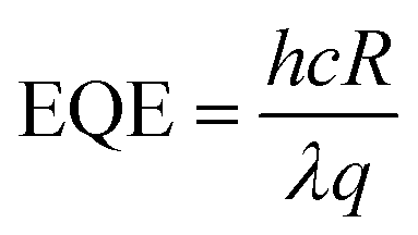 , assuming EQE = 1 for a traditional photovoltaic diode, the final R is calculated by dividing the corresponding wavelength by 1240. We can determine that the theoretical R value is 428 mA W−1 under 532 nm laser irradiation. However, the maximum R is calculated to be 459 mA W−1 at a light power density of 181.44 mW cm−2, while other R values are below the theoretical value. Therefore, the corresponding EQE under this condition is slightly higher than 1. This anomalous phenomenon is probably ascribed to the photogating effect at the InP QDs/SnSe2 interface at a high light power density, which will be discussed in the context of band alignment later. Similarly, the maximum EQE value of device I is also 109% (>100%). With sufficient incident photon energy (∼2.33 eV), all individual Cu-doping InP QD layer, SnSe2 and MoTe2 at the appropriate thickness can absorb a substantial number of photons and be directly excited from the ECu to the Ec of InP QDs, rather than through the intrinsic excitation process along the bandgap of InP QDs. As for the InP QDs/SnSe2 interface, at Ebi-1 and higher light power density, a large number of photogenerated electrons within the SnSe2 can drift and accumulate at the edge interface without overcoming the large potential barrier of the conduction band minimum, leading to the electron photogating effect across the interface. Consequently, an increasing number of photogenerated holes can be injected into the SnSe2 layer and collected by the source electrode (Fig. S14, ESI†), resulting in an EQE slightly greater than 100%. Similarly, we also observe other two-dimensional photodiodes that exhibit a maximum EQE at zero bias slightly exceeding 100%. For instance, the γ-InSe/graphene photodetector achieves an EQEmax of 161% in the ultraviolet spectrum,66 and the β-InSe/Au (NPs) self-powered photodetector has an EQEmax of 125%,67 due to carrier multiplication in semiconductors, where the absorption of a single high-energy photon generates two or more electron–hole pairs. In the near infrared spectrum, the EQEmax of the PbS QDs/MoS2/WSe2 photodiodes exceeds 100% at low light power.39 In contrast, the EQE value for the SnSe2/MoTe2 device is only 26%. In Fig. S15 (ESI†), we compared the photoelectric performance of the InP (No-doped) QDs, and found that these QDs do not enhance the performance of SnSe2/MoTe2 heterojunction photodetectors under a 532 nm laser. The reason for this is that the band gap of the InP (No-doped) QDs (∼3.38 eV) is greater than the photon energy of 532 nm light (∼2.33 eV). Comparable improvements were observed under 405 nm and 635 nm illumination, as shown in Fig. S16 and S17 (ESI†). The Ilight/Idark ratio, extracted from Fig. 3(b) and Fig. S11b (ESI†) as a function of P, is illustrated in Fig. 3(h). At the lowest P, the Ilight/Idark ratios for device I are 1.52 and 109.46, respectively. At the highest P, these ratios can be enhanced to 6.21 × 10³ and 2.06 × 10⁶. This suggests that the photosensitivity of device I is excellent independent of P because of the suppression of Idark and the enhancement of photocurrent. To analyze the tunneling process across the heterostructure in the forward current region, the Ids–Vds data in the range of 0–0.3 V can be fitted (the calculation method is detailed in Note S5, ESI†). Fig. 3(i) shows that all ln(Ids/Vds2)–ln(1/Vds) curves at various light power densities exhibit a strong linear relationship, indicating that direct tunneling (DT) transport is the predominant mechanism under positive bias conditions.23 For the SnSe2/MoTe2 heterostructure, the incorporation of InP QDs does not alter the DT process across the heterojunction at forward bias. Meanwhile, band-to-band tunneling (BTBT) can be observed in both SnSe2/MoTe2 and InP/SnSe2/MoTe2 heterostructures after fitting the Ids–Vds curve at reverse bias using the equation provided in Note S5 (ESI†), leading to the backward rectification behavior, as shown in Fig. S18 (ESI†). Finally, the corresponding band alignments under illumination at Vds > 0 V and Vds < 0 V for SnSe2/MoTe2 and InP/SnSe2/MoTe2 heterostructures are discussed in Note S5 and Fig. S19 (ESI†). It is noteworthy that the photocurrent is significantly enhanced at forward bias compared to the BTBT region because of the photo-assisted DT process.
 | ||
| Fig. 3 Photovoltaic properties of device I under 532 nm laser irradiation (a) Ids–Vds curves at different light power densities. (b) The time-resolved photoresponse at various light power densities. (c) Variation of Isc and Voc with the light power density. (d) The electrical power as a function of Vds at various illumination intensities. (e) SPCM image of the device III heterojunction at P = 2 μW with a spot diameter of 1 μm under 520 nm laser irradiation. (f) R, (g) EQE, and (h) Ilight/Idark ratio as a function of light power density. (i) DT plots of ln (Ids/Vds2) and ln (1/Vds) obtained from (a). The solid line represents the DT fitting curve of the experimental data. | ||
As shown in Fig. 4(a), the band alignment of the InP/SnSe2/MoTe2 photodetector under illumination at zero bias is investigated to explain the excellent photovoltaic performance at 532 nm. For comparison, the band alignment of SnSe2/MoTe2 at thermal equilibrium under illumination is depicted in Fig. S20 (ESI†). With sufficient incident photon energy (∼2.33 eV), the individual InP QD layer can absorb a substantial number of photons and can be directly excited from the ECu to the Ec of InP QDs (the difference between ECu and Ec is 1.96 eV), rather than through the intrinsic excitation process along the bandgap of InP QDs.57 Simultaneously, the individual SnSe2 and MoTe2 layers can also absorb photons and be excited to Ec in the intralayer direction. Under the bias condition Ebi-1, the photogenerated electrons drift and accumulate at the interface near the lnP QDs, leading to the photogating effect across the interface. Meanwhile, the photogenerated holes at the ECu of InP QDs can be driven to the Ev of SnSe2 via the interlayer direction, suggesting that hole injection or a p-type doping effect is achieved. Thus, the source terminal can collect an increasing number of holes from the SnSe2 layer with the incorporation of InP QDs. Under the bias condition Ebi-2, the photogenerated electrons drift and accumulate at the interface near MoTe2, while the photogenerated electrons return to the drain. The photogenerated holes can drift and accumulate in the SnSe2 layer. These carriers can be effectively collected at the source side due to a good ohmic contact at the SnSe2/Cr interface, leading to the appearance of negative Isc and positive Voc. Consequently, the switching speed of the interconnected device is quantified through oscilloscope analysis. To further investigate the response speed of the InP/SnSe2/MoTe2 heterojunction, we measured the rise and decay times of the device, as illustrated in Fig. 4(b). The rise and decay times of the device were found to be 1.16 ms and 1.14 ms, respectively, under 532 nm laser illumination. This represents a nearly nine-fold improvement over the response speeds of 10.02 ms and 9.01 ms observed for the SnSe2/MoTe2 heterojunction prior to spin-coating for device I (Fig. S21, ESI†). This enhancement can be attributed to the InP QD layer, which injects a large number of photogenerated holes into the SnSe2 without causing non-radiative recombination in the intralayer direction, thereby accelerating the response speed of the hybrid heterojunction. Furthermore, Fig. 4(c) shows 300 consecutive photoresponse cycles of the hybrid heterojunction device, demonstrating its reproducibility and stability. To confirm the optimal photoresponse wavelength of the device I after coating, we measured the time-dependent photoresponse curves at the wavelengths of 405 nm, 532 nm and 635 nm under strong P, as illustrated in Fig. 4(d). Although the maximum Isc increased from 1.02 nA (Fig. S16f, ESI†) and 1.24 nA (Fig. S17f, ESI†) to 5.7 nA (Fig. S16c, ESI†) and 4.43 nA (Fig. S17c, ESI†) before and after spin-coating InP QDs at 179.31 mW cm−2 and 185.71 mW cm−2 under 405 nm and 635 nm laser illumination, respectively. However, the optimal wavelength after spin-coating under the strongest P is at around 532 nm and the corresponding Ilight is as large as 53 nA. Fig. 4(e) and (f) show the trends of R and EQE as a function of P at 405 nm, 532 nm and 635 nm. In particular, the maximum R and EQE values are 44 mA W−1 and 14% at P = 3.21 mW cm−2 under the 405 nm laser, and 259 mA W−1 and 50.7% at P = 3.31 mW cm−2 under the 635 nm laser. The light power densities of the 405 nm, 532 nm and 635 nm lasers used to measure the photoresponse of the device are sufficiently strong, on the order of 102, the effect on the variation of photocurrent is nearly negligible. Thus, it can be concluded that the 532 nm wavelength is the optimal choice for this vdWHs device. Different from the tendency under 532 nm, the R decreases as the P increases under both the 405 nm and 635 nm laser. By comparing the SnSe2/MoTe2 and InP/SnSe2/MoTe2 heterojunctions under 405 nm and 635 nm, the Isc and Voc, which were extracted from Fig. S16 and S17 (ESI†), are plotted as a function of P. After linear fitting, the α values were determined to be 0.96 and 0.82 (α < 1) under 405 nm laser, indicating that the InP QDs reduce the photogenerated carriers’ recombination and interface trapping centers.68 Meanwhile, the α values under the 635 nm laser were found to be 0.51 and 0.4 (α < 1), suggesting that the InP QDs decrease the trapping of photogenerated carriers by shallow energy level defects.69
 | ||
| Fig. 4 (a) Band diagram and the current transport mechanism of the InP/SnSe2/MoTe2 heterojunction under 532 nm laser illumination. (b) Time-resolved photocurrent of the device I. (c) Photoresponse with 300 continuous laser on/off cycles of the device I under 532 nm illumination. (d) Photoresponse switching curves of device I, at light power densities of 179 mW cm−2 for 405 nm, 181 mW cm−2 for 532 nm, and 185 mW cm−2 for 635 nm. (e) R and (f) EQE of the device I as a function of the light power density under the 405 nm, 532 nm and 635 nm illumination. | ||
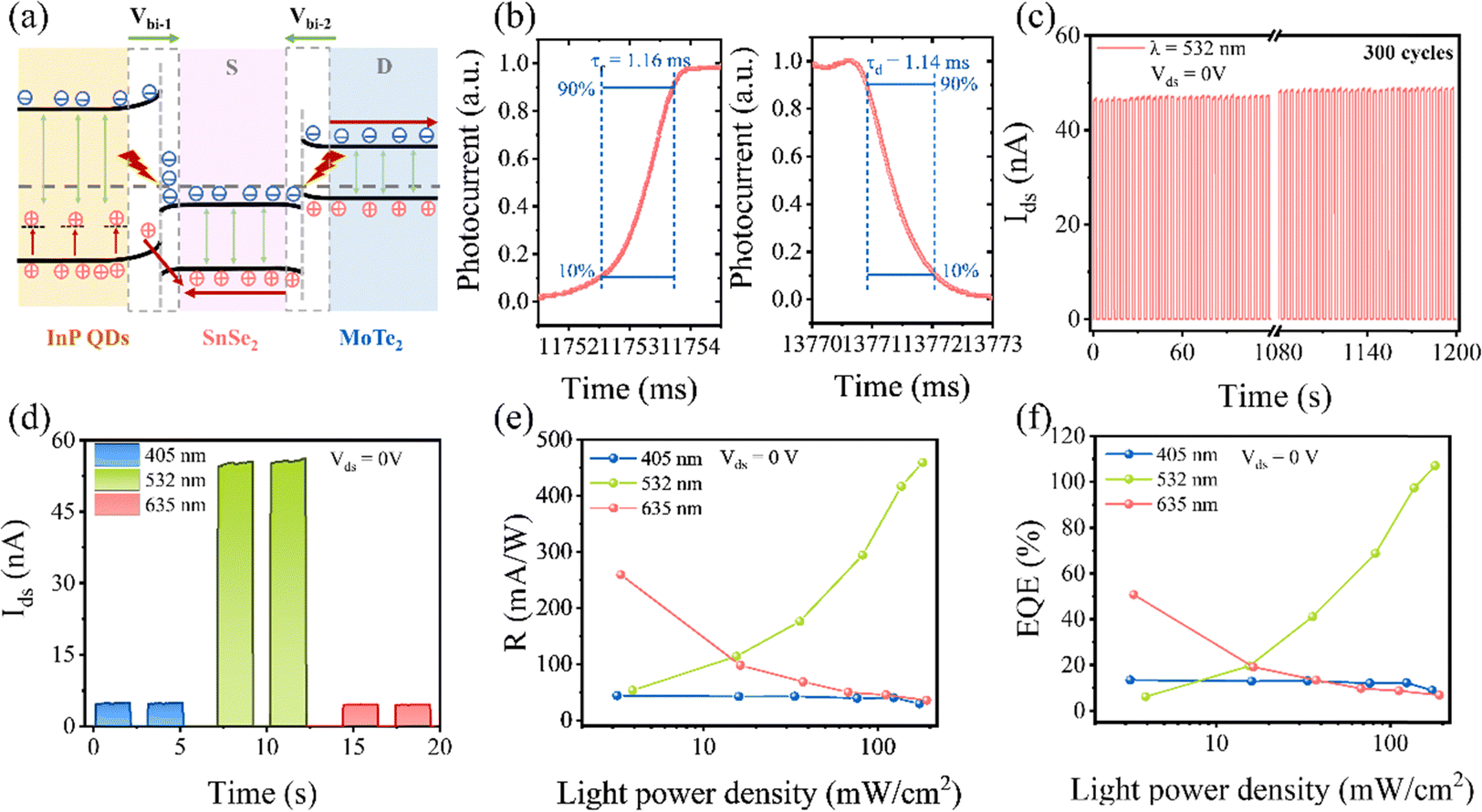
Under identical conditions to the optical measurements, the noise spectral density (Sn) was obtained as a function of frequency through Fourier transform analysis of the dark current, as shown in Fig. 5(a). At Vds = 0 V, a 1/f noise component was observed, which is attributed to interface traps or defects. When the frequency exceeds 0.18 Hz and 3 Hz, respectively, the InP/SnSe2/MoTe2 and SnSe2/MoTe2 devices exhibit low white noise levels of 4.02 and 76.7 fA Hz−1/2, respectively. Beyond the above frequencies, both the Sn are frequency-independent and approach the shot noise background. Thus, the incorporation of InP QDs can suppress the Sn and low down the translated frequency point. Moreover, NEP is expressed as the noise current (in) divided by the R. As a result, the NEP of the InP/SnSe2/MoTe2 and SnSe2/MoTe2 devices reach 0.87 × 10⁻² pW Hz−1/2 and 0.69 pW Hz−1/2, respectively (In Note S4, ESI†). It indicates that the NEP value of InP/SnSe2/MoTe2 is two orders of magnitude lower than that before spin-coating. As illustrated in Fig. 5(b), there is a significant discrepancy between the D* values calculated using different equations. The unrealistic D* value is calculated to be 9.2 × 10¹² Jones, which does not account for thermal and shot noise, and is approximately two orders of magnitude higher than the noise-derived result. In contrast, the actual D* value is calculated to be 1.45 × 10¹¹ Jones (Note S4, ESI†). Meanwhile, the unrealistic and actual D* values for SnSe2/MoTe2 are as moderate as 1.1 × 10¹⁰ Jones and 1.1 × 10⁹ Jones, respectively (Fig. S22, ESI†). In general, thickness engineering can significantly influence the photoresponse performance of 2D photodetectors. The maximum R, EQE, and D* and the enhanced factor after spin-coating can vary with different thicknesses of the top SnSe2 and bottom MoTe2. Fig. 5(c)–(e) depict the comparison of R, EQE, and D* for three devices. The variations in these parameters are primarily attributed to the various thicknesses (In Fig. S23 and S25, ESI†). The optoelectronic performance of device II and III is shown in Fig. S24–S26 (ESI†). After calculating, device III exhibits the best performance in terms of R and EQE, while device I achieves the highest D* value. A comparison of the Idark values for the three devices can be seen in Fig. S27 (ESI†). Overall, device I demonstrates comprehensive performance, and the enhancement factor before and after spin-coating InP QDs is the highest. Notably, the key advantage of device I lies in its R and EQE in the visible region, which surpasses that of other self-driven heterojunction photodetectors, as highlighted in Fig. 5(f). These include 2D heterojunction structures,21,22,70–73 Schottky barrier structures,74,75 and nanocrystal/2D materials.76 This demonstrates the superior photovoltaic performance of our hybrid heterostructure with moderated thickness, high quality Cu-doped InP QDs and the engineered band alignment.
 | ||
| Fig. 5 (a) Noise spectral density of the device I at zero bias. (b) The unrealistic D* and the actual D* of the device I as a function of the incident light power density. Comparison of R, EQE, D* of three devices (c)–(e). The thicknesses of SnSe2/MoTe2 devices I, II and III are 30/20 nm, 40/20 nm and 53/33 nm, respectively. (f) Benchmarking of R and EQE of various self-driven devices under the visible region. | ||
Conclusions
In this study, an InP/SnSe2/MoTe2 heterojunction photodetector was successfully fabricated, with the incorporation of InP QDs significantly enhancing its photovoltaic performance. By introducing hole-trapping Cu dopants, improved separation and transfer of photogenerated carriers were achieved in the InP QDs. The type-III SnSe2/MoTe2 heterojunction offers a platform for BTBT and DT devices due to its broken-gap band offset and sharp band edges. Energy band engineering was employed to form type-II and type-III InP/SnSe2/MoTe2 heterojunctions. At a wavelength of 532 nm, the device exhibited an R value of 459 mA W−1, and an EQE exceeding 100%, with a peak value reaching 109%. Furthermore, through optimization of the device structure, the dark current was significantly reduced to near-noise levels, resulting in a NEP as low as 8.7 × 10⁻³ pW Hz−1/2, a specific detectivity of 1.45 × 10¹¹ Jones, a large Ilight/Idark ratio of 106 and a swift response time of 1.16 ms/1.14 ms with stable operation. Compared to conventional heterojunction photodetectors, the self-powered device developed in this study demonstrated superior photoresponse and high stability, indicating its potential for visible light detection applications. In summary, the introduction of InP QDs provides a feasible approach for enhancing the photovoltaic response of the SnSe2/MoTe2 heterojunction, laying a foundation for the future development of high-performance self-driven photodetectors.Experimental section
Synthesis of InP/ZnSeS:Cu/ZnS QDs
InP QDs were synthesized following the procedures reported by Won et al. and Chen et al.45,54 InCl3 (0.16 mmol), Zn-oleate (1 mL), THF (1 mL), and ODE (8 mL) were combined in a three-necked flask. The solution was degassed at room temperature for 30 min before being heated to 280 °C under an Ar atmosphere. The phosphorus precursor was injected at 280 °C under an Ar atmosphere. Thirty seconds later, 0.4 mL of selenium precursor was injected dropwise at a rate of 0.333 mL h−1 using an injection pump. Subsequently, the copper precursor (4.8 μmol) was injected at 280 °C and maintained for 0.5 h. At the end of this period, Zn-oleate (2 mL) was injected when the temperature reached 300 °C. Finally, the sulfur precursor (0.5 mL) was injected dropwise at a rate of 1 mL h−1 using the injection pump. The reaction mixture was then cooled to room temperature, and the crude product was purified with acetone and re-dispersed in octane.Characterization of InP/ZnSeS:Cu/ZnS QDs
Transmission electron microscopy (TEM) and high-resolution TEM (HRTEM) images were acquired with a JEM-2100HR microscope at 200 kV. The energy dispersive X-ray spectroscopy (EDS) elemental mapping was tested using SEM-EDS (Phenom Pharos G2). The UV-vis absorption spectra and photoluminescence (PL) spectrum were carried out using a fiber optic spectrometer (QEPRO). VB-XPS spectra were obtained using an AXIS SUPRA. The spectral response of heterojunctions from 250 to 1500 nm was studied by a variable-wavelength photocurrent instrument (MStarter ABS DUV-NIR Microscopic Absorption Spectroscopy System, Nanjing Metatest Optoelectronics Co., Ltd).Fabrication of SnSe2/MoTe2 and InP/SnSe2/MoTe2 heterojunction devices
MoTe2 and SnSe2 bulk crystals are bought from Taizhou SUNANO New Energy Co., Ltd. They were exfoliated using mechanical exfoliation methods with 3M Scotch tape. SnSe2 was exfoliated onto a PDMS film (17 mil, Gel pak, bought from Shanghai Onway Technology Co., Ltd). While MoTe2 was placed on a SiO2/Si substrate. The SnSe2/MoTe2 heterojunction was fabricated using a simple three-axis manipulator platform equipped with a micromanipulator (Shanghai Onway Technology Co., Ltd). Electrodes (Cr/Au, 10/50 nm) were fabricated using a positive photoresist (AR-P 5350 of ALLRESIST GmbH Company bought from Taizhou SUNANO New Energy Co., Ltd), an Ultraviolet maskless lithography machine (TuoTuo Technology (Suzhou) Co., Ltd), developing solution (AR 300-26, supplied by ALLRESIST GmbH Company bought from Taizhou SUNANO New Energy Co., Ltd) and electron beam evaporation. The device can be obtained by immersing into the acetone and deionized water several times. The InP/SnSe2/MoTe2 structure was subsequently prepared on the SnSe2/MoTe2 heterojunction. The spin-coating speed was set to 2000 rpm for 30 seconds, during which 40 μL of a 15 mg mL−1 QD solution was deposited onto the substrate, a process that was repeated twice. The speed was then increased to 3000 rpm, and 50 μL of an EDT solution (2 vol% in acetonitrile) was added. Finally, 70 μL of acetonitrile was used for washing. The device was then placed on a heating stage at 80 °C for 5 minutes.Characterization and measurement
The morphology and dimensions of the devices were characterized using an optical microscope (ECLIPSE LV150N, Nikon). The thickness was measured with a high-resolution atomic force microscope (Cypher ES). KPFM measurement was performed using a scanning probe microscope (Bruker Dimension FastScan). The Raman spectra and PL spectrum were obtained using a confocal microscope with a laser wavelength of 532 nm (Nost Technology Co., Ltd). Corresponding ARPRS was measured with the help of an x–y piezo scan stage. The spectral response of heterojunctions from 250 to 1000 nm was studied using a variable-wavelength photocurrent instrument (MStarter ABS DUV-NIR Microscopic Absorption Spectroscopy System, Nanjing Metatest Optoelectronics Co., Ltd). All optoelectronic properties of the devices were tested using a three-probe stage with a Keithley 2636B sourcemeter. The photoresponse performance of the devices was evaluated using a fiber-coupled laser system with wavelengths of 405 nm and 635 nm. In particular, the 532 nm laser modulus (15 × 55 mm, P ≤ 50 mW) is supported by a voltage regulator. The light power density was calibrated using a power meter (PM400, Thorlabs). The high-resolution response curve was tested by using a digital oscilloscope (Siglent SDS5104X) in conjunction with the sourcemeter. SPCM was conducted using a photocurrent imaging instrument (MStarter 200 High Precision Photocurrent Scanning Test Microscope) (supplied by Nanjing Metatest Optoelectronic Co., Ltd). The noise spectrum density was measured using a low frequency noise test system (LFN-1000, Wuxi Xinjian Semiconductor-Tech Co., Ltd).Data availability
Data will be made available on request.Conflicts of interest
The authors declare no conflicts of interest.Acknowledgements
We acknowledge the financial support from the National Natural Science Foundation of China (no. 22102058, 62004071, and 62175040), the Basic and Applied Basic Research Foundation of Guangdong Province (no. 2024A1515012019 and 2024A1515012688), and the Science and Technology Program of Guangzhou (202103030001).References
- E. R. Fossum and D. B. Hondongwa, IEEE J. Electron Devices Soc., 2014, 2, 33–43 CAS.
- H. Jin, C. Park, H. H. Byun, S. H. Park and S. Y. Choi, ACS Photonics, 2023, 10, 3027–3034 CrossRef CAS.
- Y. Niu, X. Zhou, W. Gao, M. Fu, Y. Duan, J. Yao, B. Wang, M. Yang, Z. Zheng and J. Li, ACS Nano, 2023, 17, 13760–13768 CrossRef CAS PubMed.
- F. H. L. Koppens, T. Mueller, P. Avouris, A. C. Ferrari, M. S. Vitiello and M. Polini, Nat. Nanotechnol., 2014, 9, 780–793 CrossRef CAS PubMed.
- W. J. Chen, R. R. Liang, S. Q. Zhang, Y. Liu, W. J. Cheng, C. H. Sun and J. Xu, Nano Res., 2020, 13, 127–132 CrossRef CAS.
- M. Z. Bellus, M. Li, S. D. Lane, F. Ceballos, Q. N. Cui, X. C. Zeng and H. Zhao, Nanoscale Horiz., 2017, 2, 31–36 RSC.
- R. Cheng, D. H. Li, H. L. Zhou, C. Wang, A. X. Yin, S. Jiang, Y. Liu, Y. Chen, Y. Huang and X. F. Duan, Nano Lett., 2014, 14, 5590–5597 CrossRef CAS PubMed.
- M. M. Furchi, A. Pospischil, F. Libisch, J. Burgdörfer and T. Mueller, Nano Lett., 2014, 14, 4785–4791 CrossRef CAS PubMed.
- Y. Q. Liu, C. H. Lu, M. W. Luo, T. T. Han, Y. Q. Ge, W. Dong, X. Y. Xue, Y. X. Zhou and X. L. Xu, Nanoscale Horiz., 2022, 7, 1217–1227 RSC.
- J. Lee, N. T. Duong, S. Bang, C. Park, D. A. Nguyen, H. Jeon, J. Jang, H. M. Oh and M. S. Jeong, Nano Lett., 2020, 20, 2370–2377 CrossRef CAS PubMed.
- L. Tao, B. Yao, Q. Yue, Z. Y. Dan, P. T. Wen, M. M. Yang, Z. Q. Zheng, D. X. Luo, W. J. Fan, X. Z. Wang and W. Gao, Nanoscale, 2021, 13, 15403–15414 RSC.
- R. S. Yan, S. Fathipour, Y. M. Han, B. Song, S. D. Xiao, M. D. Li, N. Ma, V. Protasenko, D. A. Muller, D. Jena and H. G. Xing, Nano Lett., 2015, 15, 5791–5798 CrossRef CAS PubMed.
- S. Chen, J. Ma, N. Bu, T. Zheng, J. Chen, J. Huang, X. Luo, Z. Zheng, N. Huo, J. Li and W. Gao, ACS Appl. Mater. Interfaces, 2024, 16, 33740–33751 CrossRef CAS PubMed.
- X. Luo, Y. S. Liu, T. Zheng, L. Huang, Z. Q. Zheng, J. M. Huang, Z. B. Lan, L. Zhao, J. Y. Ma, N. J. Huo, Y. Yan, Y. Berencén, W. Gao and J. B. Li, ACS Appl. Mater. Interfaces, 2024, 16, 42491–42501 CrossRef CAS PubMed.
- J. Na, Y. Kim, J. H. Smet, M. Burghard and K. Kern, ACS Appl. Mater. Interfaces, 2019, 11, 20973–20978 CrossRef CAS PubMed.
- C. Y. Tan, S. Q. Yin, J. W. Chen, Y. Lu, W. S. Wei, H. F. Du, K. L. Liu, F. K. Wang, T. Y. Zhai and L. Li, ACS Nano, 2021, 15, 8328–8337 CrossRef CAS PubMed.
- X. Wei, F. Yan, Q. Lv, C. Shen and K. Wang, Nanoscale, 2017, 9, 8388–8392 RSC.
- F. Yan, L. Zhao, A. Patane, P. Hu, X. Wei, W. Luo, D. Zhang, Q. Lv, Q. Feng, C. Shen, K. Chang, L. Eaves and K. Wang, Nanotechnology, 2017, 28, 27LT01 CrossRef PubMed.
- Z. Wenkai, W. Xia, Y. Faguang, L. V. Quanshan, H. Ce and W. Kaiyou, J. Semicond., 2019, 40, 092001 CrossRef.
- Q. Lv, F. Yan, X. Wei and K. Wang, Adv. Opt. Mater., 2018, 6, 1700490 CrossRef.
- P. K. Srivastava, Y. Hassan, Y. Gebredingle, J. Jung, B. Kang, W. J. Yoo, B. Singh and C. Lee, ACS Appl. Mater. Interfaces, 2019, 11, 8266–8275 CrossRef CAS PubMed.
- L. W. Wu, W. Gao, Y. M. Sun, M. M. Yang, Z. Q. Zheng, W. J. Fan, K. X. Shu, Z. Y. Dan, N. Zhang, N. J. Huo and J. B. Li, Adv. Mater. Interfaces, 2022, 9, 2102099 CrossRef CAS.
- X. Zhou, X. Z. Hu, S. S. Zhou, H. Y. Song, Q. Zhang, L. J. Pi, L. Li, H. Q. Li, J. T. Lü and T. Y. Zhai, Adv. Mater., 2018, 30, 1703286 CrossRef PubMed.
- X. N. Cong, Y. Zheng, F. Huang, Q. You, J. Tang, F. Fang, K. Jiang, C. Han and Y. M. Shi, Nano Res., 2022, 15, 8442–8450 CrossRef CAS.
- K. Iordanidou and J. Wiktor, Phys. Rev. Mater., 2022, 6, 084001 CrossRef CAS.
- H. Yan, Q. Zhao, Y. Chen, S. Wu, G. Li, X. Da, H. Jiao, X. Tai, Y. Xiao, S. Yan, M. Tang, T. Lin, H. Shen, X. Meng, X. Wang, J. Chu and J. Wang, IEEE Trans. Electron Devices, 2023, 70, 5966–5971 CAS.
- F. Zhang, H. Shi, Y. Yu, S. Liu, D. Liu, X. Zhou, L. Yuan, J. Shi, Q. Xia, Z. Wei, J. He and M. Zhong, Adv. Opt. Mater., 2024, 12, 2303088 CrossRef CAS.
- Z. Li, T. Zheng, M. Yang, Y. Sun, D. Luo, W. Gao, Z. Zheng and J. Li, Adv. Opt. Mater., 2024, 12, 2400023 CrossRef CAS.
- J. Ma, S. Chen, L. Zhao, J. Chen, Z. Lan, M. Yang, Y. Sun, Z. Zheng, W. Gao and J. Li, Adv. Opt. Mater., 2024, 12, 2302563 CrossRef CAS.
- M. H. Jiang, T. Zheng, J. L. Zhang, Z. M. Li, Q. R. Deng, Y. Pan, W. Gao, Y. J. Yang, J. B. Li and N. J. Huo, Adv. Opt. Mater., 2024, 12, 2303217 CrossRef CAS.
- X. N. Han, P. T. Wen, L. Zhang, W. Gao, H. Y. Chen, F. Gao, S. H. Zhang, N. J. Huo, B. S. Zou and J. B. Li, ACS Appl. Mater. Interfaces, 2021, 13, 61544–61554 CrossRef CAS PubMed.
- Y. M. Sun, J. X. Xiong, X. M. Wu, W. Gao, N. J. Huo and J. B. Li, Nano Res., 2022, 15, 5384–5391 CrossRef CAS.
- M. J. Grotevent, C. U. Hail, S. Yakunin, D. Bachmann, G. Kara, D. N. Dirin, M. Calame, D. Poulikakos, M. V. Kovalenko and I. Shorubalko, ACS Appl. Mater. Interfaces, 2021, 13, 848–856 CrossRef CAS PubMed.
- J. Luo, G. S. Selopal, X. Tong and Z. Wang, Electron, 2024, 2, e30 CrossRef CAS.
- D. Kufer and G. Konstantatos, ACS Photonics, 2016, 3, 2197–2210 CrossRef CAS.
- R. Pan, H. Y. Li, J. Wang, X. Jin, Q. H. Li, Z. M. Wu, J. Gou, Y. D. Jiang and Y. L. Song, Part. Part. Syst. Charact., 2018, 35, 1700304 CrossRef.
- H. L. Wu, H. N. Si, Z. H. Zhang, Z. Kang, P. W. Wu, L. X. Zhou, S. C. Zhang, Z. Zhang, Q. L. Liao and Y. Zhang, Adv. Sci., 2018, 5, 1801219 CrossRef PubMed.
- Z. Y. Dan, C. L. Wang, W. Gao, K. X. Shu, L. W. Wu, W. Z. Wang, Q. X. Zhao, X. J. Liu, X. Liu, N. J. Huo and J. B. Li, APL Mater., 2021, 9, 081117 CrossRef CAS.
- P. Y. Zeng, W. H. Wang, D. S. Han, J. D. Zhang, Z. H. Yu, J. Y. He, P. Zheng, H. Zheng, L. Zheng, W. T. Su, D. X. Huo, Z. H. Ni, Y. Zhang and Z. T. Wu, ACS Nano, 2022, 16, 9329–9338 CrossRef CAS PubMed.
- S. F. Wang, A. Ashokan, S. Balendhran, W. Yan, B. C. Johnson, A. Peruzzo, K. B. Crozier, P. Mulvaney and J. Bullock, ACS Nano, 2023, 17, 11771–11782 CrossRef CAS PubMed.
- B. Chen, D. Y. Li and F. Wang, Small, 2020, 16, 2002454 CrossRef CAS PubMed.
- Y. Wang, J. Howley, E. N. Faria, C. Huang, S. Carter-Searjeant, S. Fairclough, A. Kirkland, J. J. Davis, F. Naz, M. T. Sajjad, J. M. Goicoechea and M. Green, Nanoscale Horiz., 2023, 8, 1411–1416 RSC.
- P. Ramasamy, B. Kim, M. S. Lee and J. S. Lee, Nanoscale, 2016, 8, 17159–17168 RSC.
- T. Kim, S. W. Kim, M. Kang and S. W. Kim, J. Phys. Chem. Lett., 2012, 3, 214–218 CrossRef CAS.
- Y. H. Won, O. Cho, T. Kim, D. Y. Chung, T. Kim, H. Chung, H. Jang, J. Lee, D. Kim and E. Jang, Nature, 2019, 575, 634–638 CrossRef CAS PubMed.
- H. Zhao, H. Hu, J. Zheng, Y. Qie, K. Yu, Y. Zhu, Z. Luo, L. Lin, K. Yang, T. Guo and F. Li, ACS Appl. Nano Mater., 2023, 6, 3797–3802 CrossRef CAS.
- J. P. Park, J. J. Lee and S. W. Kim, Sci. Rep., 2016, 6, 30094 CrossRef CAS PubMed.
- P. Wu and X. P. Yan, Chem. Soc. Rev., 2013, 42, 5489–5521 RSC.
- J. Hasanzadeh and S. F. Shayesteh, Eur. Phys. J.: Appl. Phys., 2010, 51, 30601–30605 CrossRef.
- H. Zhao, X. Li, M. Cai, C. Liu, Y. You, R. Wang, A. I. Channa, F. Lin, D. Huo, G. Xu, X. Tong and Z. M. Wang, Adv. Energy Mater., 2021, 11, 2101230 CrossRef CAS.
- D. Mocatta, G. Cohen, J. Schattner, O. Millo, E. Rabani and U. Banin, Science, 2011, 332, 77–81 CrossRef CAS PubMed.
- S. Jana, B. B. Srivastava, S. Jana, R. Bose and N. Pradhan, J. Phys. Chem. Lett., 2012, 3, 2535–2540 CrossRef CAS PubMed.
- J. Luo, X. Tong, S. Yue, K. Wu, X. Li, H. Zhao, B. Wang, Z. Li, X. Liu and Z. M. Wang, ACS Nano, 2024 Search PubMed.
- X. Chen, Y. Guo, J. Li, H. Yang, Z. Chen, D. Luo and X. Liu, Chem. Eng. J., 2024, 496, 153947 CrossRef CAS.
- M. P. A. Muthalif, Y. S. Lee, C. D. Sunesh, H. J. Kim and Y. Choe, Appl. Surf. Sci., 2017, 396, 582–589 CrossRef CAS.
- Z. Zhang, J. B. Yi, J. Ding, L. M. Wong, H. L. Seng, S. J. Wang, J. G. Tao, G. P. Li, G. Z. Xing, T. C. Sum, C. H. A. Huan and T. Wu, J. Phys. Chem. C, 2008, 112, 9579–9585 CrossRef CAS.
- J. Bang, S. Das, E. J. Yu, K. Kim, H. Lim, S. Kim and J. W. Hong, Nano Lett., 2020, 20, 6263–6271 CrossRef CAS PubMed.
- B. B. Srivastava, S. Jana and N. Pradhan, J. Am. Chem. Soc., 2011, 133, 1007–1015 CrossRef CAS PubMed.
- R. G. Xie and X. G. Peng, J. Am. Chem. Soc., 2009, 131, 10645–10651 CrossRef CAS PubMed.
- L. Hu, Z. L. Zhang, R. J. Patterson, Y. C. Hu, W. J. Chen, C. Chen, D. B. Li, C. Hu, C. Ge, Z. H. Chen, L. Yuan, C. Yan, N. Song, Z. L. Teh, G. J. Conibeer, J. Tang and S. J. Huang, Nano Energy, 2018, 46, 212–219 CrossRef CAS.
- J. D. Lin, C. Han, F. Wang, R. Wang, D. Xiang, S. Q. Qin, X. A. Zhang, L. Wang, H. Zhang, A. T. S. Wee and W. Chen, ACS Nano, 2014, 8, 5323–5329 CrossRef CAS PubMed.
- T. Roy, M. Tosun, M. Hettick, G. H. Ahn, C. M. Hu and A. Javey, Appl. Phys. Lett., 2016, 108, 083111 CrossRef.
- M. W. Iqbal, E. Elahi, A. Amin, S. Aftab, I. Aslam, G. Hussain and M. A. Shehzad, Superlattices Microstruct., 2020, 147, 106698 CrossRef CAS.
- H. Yu, Y. Wang, H. Zeng, Z. Cao, Q. Zhang, L. Gao, M. Hong, X. Wei, Y. Zheng, Z. Zhang, X. Zhang and Y. Zhang, ACS Nano, 2024, 18, 17100–17110 CrossRef CAS PubMed.
- X. Meng, Y. Du, W. Wu, N. B. Joseph, X. Deng, J. Wang, J. Ma, Z. Shi, B. Liu, Y. Ma, F. Yue, N. Zhong, P.-H. Xiang, C. Zhang, C.-G. Duan, A. Narayan, Z. Sun, J. Chu and X. Yuan, Adv. Sci., 2023, 10, 2300413 CrossRef CAS PubMed.
- Y. Z. Li, J. Y. Pan, C. X. Yan, J. X. Li, W. Xin, Y. T. Zhang, W. Z. Liu, X. F. Liu, H. Y. Xu and Y. C. Liu, Nano Lett., 2024, 24, 7252–7260 CrossRef CAS PubMed.
- M. J. Dai, H. Y. Chen, R. Feng, W. Feng, Y. X. Hu, H. H. Yang, G. B. Liu, X. S. Chen, J. Zhang, C. Y. Xu and P. A. Hu, ACS Nano, 2018, 12, 8739–8747 CrossRef CAS PubMed.
- N. Guo, W. D. Hu, L. Liao, S. Yip, J. C. Ho, J. S. Miao, Z. Zhang, J. Zou, T. Jiang, S. W. Wu, X. S. Chen and W. Lu, Adv. Mater., 2014, 26, 8203–8209 CrossRef CAS PubMed.
- W. Gao, S. Zhang, F. Zhang, P. T. Wen, L. Zhang, Y. M. Sun, H. Y. Chen, Z. Q. Zheng, M. M. Yang, D. X. Luo, N. J. Huo and J. B. Li, Adv. Electron. Mater., 2021, 7, 2000964 CrossRef CAS.
- D. Li, B. Wang, M. Chen, J. Zhou and Z. Zhang, Small, 2017, 13, 1603726 CrossRef PubMed.
- Y. Xie, E. X. Wu, J. Zhang, X. D. Hu, D. H. Zhang and J. Liu, ACS Appl. Mater. Interfaces, 2019, 11, 14215–14221 CrossRef CAS PubMed.
- A. Y. Gao, E. F. Liu, M. S. Long, W. Zhou, Y. Y. Wang, T. L. Xia, W. D. Hu, B. G. Wang and F. Miao, Appl. Phys. Lett., 2016, 108, 223501 CrossRef.
- X. Liu, G. Z. Sun, P. Chen, J. C. Liu, Z. W. Zhang, J. Li, H. F. Ma, B. Zhao, R. X. Wu, W. Q. Dang, X. D. Yang, C. Dai, X. W. Tang, Z. J. Chen, L. L. Miao, X. Q. Liu, B. Li, Y. Liu and X. D. Duan, Nano Res., 2019, 12, 339–344 CrossRef CAS.
- J. L. Du, Q. L. Liao, B. S. Liu, X. K. Zhang, H. H. Yu, Y. Ou, J. K. Xiao, Z. Kang, H. N. Si, Z. Zhang and Y. Zhang, Adv. Funct. Mater., 2021, 31, 2007559 CrossRef CAS.
- J. Huang, K. Shu, N. Bu, Y. Yan, T. Zheng, M. Yang, Z. Zheng, N. Huo, J. Li and W. Gao, Sci. China Mater., 2023, 66, 4575–4586 CrossRef.
- K. C. Gao, S. L. Ran, Q. Han, Q. Yang, H. Jiang, J. T. Fu, C. Q. Leng, S. L. Feng, D. H. Zhou, Z. C. Li, X. Li, D. P. Huang, L. Y. Yu and J. Shen, Opt. Mater., 2022, 124, 112013 CrossRef CAS.
Footnotes |
| † Electronic supplementary information (ESI) available. See DOI: https://doi.org/10.1039/d4nh00663a |
| ‡ These authors contributed equally to this work. |
| This journal is © The Royal Society of Chemistry 2025 |