
Phase-change wax integrated with a rapid carbon nanotube array for spatial light modulation†
Liwen
Lai
ab,
Peng
Liu
 *b,
Chunhai
Zhang
b,
Duanliang
Zhou
b,
Qunqing
Li
*b and
Shoushan
Fan
b
*b,
Chunhai
Zhang
b,
Duanliang
Zhou
b,
Qunqing
Li
*b and
Shoushan
Fan
b
aTsinghua Shenzhen International Graduate School, Tsinghua University, Shenzhen 518055, China
bDepartment of Physics, Tsinghua-Foxconn Nanotechnology Research Center, Tsinghua University, Beijing 100084, China. E-mail: pengliu@tsinghua.edu.cn
First published on 5th May 2025
Abstract
By integrating super-aligned carbon nanotube (SACNT) films with paraffin wax, an addressable optical valve composite array was created through screen printing and laser cutting. The temperature of the SACNT film can be controlled, which rapidly induces phase changes in the paraffin wax, leading to a swift change in optical transparency. The transmission spot exhibited significant differences, with a contrast degree reaching up to 0.65. At a paraffin wax surface density of 1.17 × 10⁻⁴ g mm−2, the rise and fall times of the transmitted optical signal across the 350–1100 nm spectrum were 155 ± 2 ms and 135 ± 11 ms, respectively, enabling rapid spatial light modulation. A prototype was fabricated, capable of dynamically displaying letters, with the crosstalk effect of the current being significantly mitigated in spatial light modulation. This rapid spatial light modulation prototype can be customized to any shape and size, and it can either be freestanding or mounted on any substrate. This innovation offers a new approach to spatial light modulation.
New conceptsA new approach to effective spatial light modulation with swift change is demonstrated by integrating a super-aligned carbon nanotube film array with paraffin wax. An addressable prototype is fabricated through screen printing and laser cutting, capable of dynamically displaying letters, with the crosstalk effect of the current being significantly mitigated in spatial light modulation. The preparation and implementation of the entire array eliminate the need for precise moving parts and complex fabrication processes, which are typically essential for spatial light modulation research involving digital micro-mirror devices, liquid crystals and meta-surfaces. This rapid addressable prototype can be customized to any shape and size, and either be freestanding or mounted on any substrate. This study serves as a prime example of actively controlling macroscopic optical phenomena through nanofilms, bypassing high cost associated with the MEMS process of preparing self-supporting films and facilitating the creation of large-area thin film arrays. Compared to research utilizing a single-layer SACNT film as a heater, fabricating the SACNT film into a heater array enables more efficient and addressable control, with the potential for more sophisticated electronic control designs. Additionally, whether used as a thermal resistance array or in conjunction with phase change materials, this study offers new possibilities for thermal radiation control applications. |
1. Introduction
A super-aligned carbon nanotube (SACNT) film is a novel type of material. Owing to the strong van der Waals interactions, it can be directly drawn from vertically aligned carbon nanotube (CNT) arrays grown on silicon wafers by a low-pressure chemical vapor deposition method.1,2 This process results in films with parallel-aligned and uniformly distributed CNT bundles throughout. Boasting the exceptional properties of mass production, and an ultrathin, conductive, transparent, flexible, stretchable and uniform structure with high emissivity,3–5 the freestanding SACNT film has opened up broad research fields. In previous work, a polarized infrared thermal detector,5 transparent and stretchable conductors,3 a femtonewton torsional balance6 and a broadband omnidirectional perfect absorber7 were successfully fabricated. The SACNT film can be simply patterned using laser cutting, employed as masks in micromachining processes to create microstructures with superior performance,8,9 or transformed into a porous array.10Recently, the SACNT film has been successfully utilized as an infrared light source in non-dispersive infrared greenhouse-gas monitoring11 and as a transparency-switchable actuator.12 These applications capitalize on the ultra-small heat capacity per unit area (HCPUA),13 rapid thermal response14 (with ramp-up and cool-down times in the sub-millisecond range), and ease of fabrication and cutting. The HCPUA of a 700 nm thick copper foil is 2.0 J m−2 K−1, whereas the HCPUA of the SACNT film is a mere 7.7 × 10⁻³ J m−2 K−1.13 Like porous carbon, the porous and network structure of the SWCNT (single wall carbon nanotube) film, with an average thickness of only tens of nano-meters, results in low density, excellent thermal conductivity, and stability. Compared to metals, SACNT films are more effective at dissipating heat. Consequently, when constructing functional phase change structures with materials like paraffin wax, SACNT films offer significant thermal response advantages. The abundant benefits of SACNT films, including efficient large-area production, low density, rapid modulation, and the capacity to be cut into various shapes, suggest promising research prospects in the field of phase change functional materials. It is anticipated that SACNT films will claim a share of the market alongside metals and porous carbon.
SACNT films have been successfully applied in fast-controlled incandescence displays,14–16 rapid thermal actuators and optical control,12,17 as well as in fast adaptive thermal camouflage.18 These outstanding properties have sparked research interest in light management15–17,19 and thermal management,20–23 particularly when the SACNT film is combined with thermochromic and phase-change materials.24,25 However, there is still a scarcity in leveraging the transmitted light to exploit the transparency of SACNT films. A typical application of active optical control for transmitted light is spatial light modulation,26–32 which traditionally relies on photonic crystals,33,34 liquid crystals,35–37 surface plasma,38 meta-surfaces39–42 and phase-change materials,43,44 among others. By compositing the SACNT film with phase-change or thermochromic materials, significant changes in optical properties can be induced, especially in spatial light modulation. If this composite structure can be fabricated into an array, it would not only represent a novel research approach, but also capitalize on the benefits of array addressable control.
In this study, an addressable heater array using a SACNT-film, fabricated through screen printing and laser-cutting for phase transition and rapid spatial light modulation, is reported. The SACNT-film array is overlaid with paraffin wax, allowing the transmittance of the entire array to be modulated. Under circuit control, the paraffin wax melts as the SACNT film heats up, causing transmittance to increase significantly, changing from low in the solid state to high in the melted state, thereby achieving rapid and effective spatial light modulation. With the aid of phase change, efficient and swift spatial light modulation of the SACNT film is successfully realized. The preparation and implementation of the array eliminate the need for precise moving parts45 and complex fabrication processes,45–49 which are typically essential for spatial light modulation research involving digital micro-mirror devices, liquid crystals and meta-surfaces.
Furthermore, polarization is a critical factor for liquid crystals and meta-surfaces, which constrains their development. This research introduces new application fields for SACNT films and could have a significant impact on rapid phase-change modulation and spatial light modulation. It is expected to stimulate advancements in active optical control application, including smart windows,50–53 dynamic colour displays,54 optical switches,55 and intelligent computing.56 This study serves as a prime example of actively controlling macroscopic optical phenomena through nanofilms, bypassing the high cost associated with the MEMS process of preparing self-supporting films and facilitating the creation of large-area thin film arrays. Compared to the research utilizing a single-layer SACNT film as a heater, fabricating the SACNT film into a heater array enables more efficient and addressable control, with the potential for more sophisticated electronic control designs. Additionally, whether used as a thermal resistance array or in conjunction with phase change materials, this study offers new possibilities for thermal radiation control applications.
2. Results and discussion
2.1. Fabrication of the SACNT microheater array and the SACNT–paraffin wax composite structure
Due to its high transmittance of 92%, the sodium calcium glass sheet with a thickness of 0.33 mm was selected and used as the substrate for screen printing and composite array fabrication within the wavelength range of 350–1100 nm. The transmittance spectrum of the sodium calcium glass substrate is depicted in Fig. S1 of the ESI.† The process for preparing the SACNT film array through screen printing and laser-cutting is detailed in Fig. S2 of the ESI.† Below is a brief description of the fabrication steps.The fabrication process began with the sequential screen printing of a transverse silver electrode, an insulating dielectric layer, and a longitudinal silver electrode to form a 16 × 16 grid pattern. This established the foundation for the SACNT film microheater array. Next, the CNT electrode layer was printed, which connects the longitudinal and transverse silver electrodes and supports the SACNT films. This layer is crucial for establishing electrical continuity between the two silver electrode layers. The printed CNT electrode was then sintered at 570 °C for 30 minutes in a muffle furnace to ensure proper adhesion and conductivity. To enhance the reliability of the SACNT film on the CNT electrode, an additional CNT electrode layer was printed on top. Following this, a single-layer SACNT film was laid on the 16 × 16 grid, adhering to the slurry already present. The entire glass sheet, now patterned with the SACNT film, was heated on a hot plate at 150 °C for 5 minutes to ensure the film's adherence. The SACNT film was then precisely cut using a laser to remove excess material, resulting in a 16 × 16 SACNT film array. An optical photograph of this 16 × 16 SACNT film array is provided in Fig. S3 (ESI†). Finally, the SACNT film array was placed on a hot plate set at 100 °C, and melted paraffin wax was poured over it. Once the sample naturally cooled to room temperature, a complete SACNT–paraffin wax composite structure array was obtained. Fig. S4 (ESI†) shows an optical photograph of the final SACNT–paraffin wax composite structure array, with a surface density of paraffin wax at 2.23 × 10⁻⁴ g mm−2.
2.2. Sample characterization
An optical image of the prepared single-layer SACNT film array is shown in Fig. 1a. Fig. 1b shows a scanning electron microscopy (SEM) image of the same single-layer SACNT film. Following the fabrication of the SACNT film array, molten paraffin wax was carefully poured onto the SACNT film array, which was placed on a hot plate preheated to 100 °C. Once the entire sample had naturally cooled, a fully formed SACNT–paraffin wax composite structure array was achieved. Details of the specific fabrication process are provided in the ESI.† | ||
| Fig. 1 Optical image of the SACNT film heater array and SEM images of the single-layer SACNT film. (a) Optical image of the SACNT film array with a scale bar representing 3 mm. (b) SEM image of the single-layer SACNT film with a scale bar representing 500 μm. The inset displays a higher magnification SEM image with a scale bar of 20 μm. | ||
2.3. Comparative performance of the SACNT–paraffin wax composite structure in solid and melted paraffin wax states
By modulating the heating of a single grid point within an array, the changes in the apparent state of the paraffin wax at that grid point before and after melting were observed and recorded using a microscope. The appearance of the paraffin wax during solidification and melting is shown in Fig. 2a and b, respectively. In the solid state, only a blurry outline of the SACNT film was visible. However, upon melting, the CNT bundles became clearly discernible. Subsequently, a piece of white paper printed with an English letter was placed beneath the substrate to observe the appearance of the letter before and after the paraffin wax melted. The presence of solid paraffin wax rendered the English letter almost invisible, as illustrated in Fig. 2a. In the melted state of the paraffin wax, the English letter became visible, and the carbon powder from the printed letter was also discernible (Fig. 2c). This observation suggests a significant change in optical transmittance at the heated grid point of the composite array before and after the wax melted. Unlike the low transmittance observed in the solid state due to polycrystalline scattering, the melted paraffin wax exhibited high transmittance. Additionally, Fig. S6 and S7 (ESI†) show the melting and solidification processes of the paraffin wax, which are divided into 12 different stages, respectively. It is revealed that the SACNT film having a lower heat capacity than paraffin wax, experienced a faster temperature drop after the power was turned on and off. Consequently, the paraffin wax in proximity to the SACNT film responds more rapidly to temperature changes than the paraffin wax on the surface of the sample. | ||
| Fig. 2 Appearance of a printed English letter ‘O’ on the back of the substrate during solidification and melting of the paraffin wax, and the transmittance spectra of the SACNT–paraffin wax composite structure. (a) Paraffin wax in the solid state. (b) Paraffin wax in the melted state. (c) Appearance of the English letter “O” when the paraffin wax was in the melted state. (d) Transmittance spectra of six SACNT–paraffin wax composite samples with different paraffin wax densities from 1.17 × 10⁻⁴ to 6.89 × 10⁻⁴ g mm−2. (e) Transmittance spectra of the sample with a paraffin wax surface density of 2.81 × 10⁻⁴ g mm−2 during five cycles of power on and power off modulated heating. (f) Differences in the optical transmittance spectra of the sample with a paraffin wax surface density of 2.81 × 10⁻⁴ g mm−2 during five cycles of power on and power off modulated heating. | ||
2.4. Transmittance spectra of the SACNT–paraffin wax composite structure
The transmittance properties of the composite structure were examined using a microscopic spectrophotometer. Our initial investigation focused on the correlation between transmittance and the surface density of paraffin wax within the composite (Fig. 2d). Six distinct SACNT–paraffin wax composite structures, each with a varying surface density of paraffin wax ranging from 1.17 × 10⁻⁴ g mm−2 to 6.89 × 10⁻⁴ g mm−2, were tested. The findings revealed that within the wavelength range of 400–900 nm, the transmittance of the SACNT–paraffin wax composite structure decreased as the surface density of paraffin wax increased. For spatial light modulation, the optical transmittance difference between solid and melted states of paraffin wax is more important. This trend is crucial for applications involving spatial light modulation, where the difference in optical transmittance between the solid and melted states of paraffin wax is particularly significant. The ability to modulate light transmission by altering the state of the paraffin wax offers potential applications for active optical control devices. The transmittance spectra of the SACNT–paraffin wax composite structure, measured at a surface density of paraffin wax at 2.81 × 10⁻⁴ g mm−2 over five cycles of modulated heating, are depicted in Fig. 2e. In this figure, the power on and off resulted for the same cycle are represented in the same colours. Subsequently, the variations in optical transmittance spectra across the five cycles are plotted in Fig. 2f. For a paraffin wax with a surface density of 2.81 × 10⁻⁴ g mm−2, the minimum transmittance difference exceeded 48%. Moreover, the average transmittance difference within the wavelength region of 400–900 nm reached as high as 57.57%.2.5. Effective modulation of an individual light spot
By illuminating the entire array with a white light-emitting diode and positioning a white screen beneath the substrate, the alterations in the light spot on the screen, specifically beneath the target modulated grid point on the composite array, were monitored during power cycles. Fig. S7 (ESI†) shows the optical image of a periodic electric heating sample, with a paraffin wax density of 1.17 × 10⁻⁴ g mm−2, along with the labelling of rows and columns within the array. Upon activation of the power, a distinct bright spot emerged on the screen, as depicted in Fig. 3a. Following initial experimental explorations (as shown in Fig. S8 of the ESI†), the melting time constitutes approximately 55% of the cycle. Given that prolonged repeated heating can readily result in the thinning of the paraffin wax layer covering the SACNT film (as illustrated in Fig. S9 of the ESI†), a pulse with peak voltage of 6 V, a frequency of 1 Hz, and a duty cycle of 45.1% was subsequently employed to modulate the heating of the target grid point. The variation of the light spot on the white screen over time is presented in Fig. 3b. From the 1st to the 20th second, even as the cumulative modulation heating time increased from 1 to 20 seconds, no light spots appeared on the back of the other grids, indicating that no significant crosstalk phenomenon occurred. At the 18th and 20th seconds, the light spot slightly intensified with the duration of heating. This was attributed to repeated heating and melting of paraffin wax; under the influence of liquid tension, the paraffin wax in the central area (grid) of the SACNT film became thinner. In the area without the SACNT film (adjacent to the grid), the paraffin wax here gradually melts due to the heat conduction, leading to an increase in both the transmittance area and the size of the light spot. The stability of the light spot can be further enhanced through methods such as improved heat dissipation and the use of shaped light masks. For instance, constructing a closed circular or rectangular hollow closed insulation layer on the CNT electrode to prevent the flowing of paraffin wax after melting, which may lead to a gradual decrease in paraffin wax at the heating point in this area. This can prevent the thickness of paraffin from thinning and causing changes in transmittance, thereby improving the stability, repeatability, and durability of spatial light modulation performance at this point. Ultimately, this helps to improve the performance of the entire array. These phenomena are also illustrated and summarized in Fig. S9 (ESI†). | ||
| Fig. 3 Comparison of the optical photographs of the light spot in the melted and solid states of the paraffin wax, and the modulated transmitted light intensity. (a) Changes of the light spot on white paper when the power was off and on. (b) Variation of the light spot at modulated heating times of 1, 4, 8, 13, 18 and 20 s. (c) Detected transmitted light signal through a single grid point of the SACNT–paraffin wax composite structure when the composite array was modulated by a pulse. (d) Definition of the rise and fall time. | ||
2.6. Stable response of the transmitted light
The transmission light intensity of the SACNT–paraffin wax composite structure array during modulated heating was measured using a Si photodetector, as plotted in Fig. 3c. The effective area of the Si photodetector was 1 mm2, and it was sensitive to wavelengths ranging from 350–1100 nm. The transmission signal remained stable for up to 10 seconds, being synchronous with the heating voltage, which suggests that the phase change during modulation occurred very rapidly. The contrast degree of the modulated transmitted light intensity is defined as the formula (signal_max − signal_min)/(signal_max + signal_min), and the final measured value reached up to 0.65. This high contrast ratio indicates that effective spatial light modulation was achieved. Furthermore, the modulation display results for both a single light spot and a column of light spots can be viewed in the ESI† (Videos S1 and S2).The rise and fall time of the transmitted light intensity signal were subsequently measured, with their definitions illustrated in Fig. 3d. Here, the increase in the transmitted light signal that coincides with the melting of the paraffin wax is termed as the rise process, while the decrease in the transmitted light signal that accompanied solidification of the paraffin wax is termed as the fall process. For this study, the results of five cycles were averaged. The measured rise and fall time were 155 ± 2 ms and 135 ± 11 ms. These measurements demonstrate that the SACNT–paraffin wax composite structure is capable of light modulation on the order of 100 ms. There is an expectation that the response time can be further shortened in the future by employing thinner substrates and optimizing the materials used.
2.7. Infrared thermal imaging results of electrical crosstalk
An infrared thermal imager was applied to monitor the results of periodic heating of a single grid point. It revealed that the temperature at the heating grid center, caused by electric modulation heating, increased continuously over time. However, it was also observed that the high-temperature region in the thermal image formed two distinct intersecting lines radiating from the heating grid center. This observation directly demonstrates the presence of electrical crosstalk in the passive addressing circuitry. In other words, as the heating time extends, the grid points that share the same row and column as the target grid point are gradually heated as well, indicating that the electrical signal is not confined to the intended grid point but is spreading to adjacent ones, which is an undesirable effect known as crosstalk. Fig. 4 shows the infrared thermal images captured from the 2nd to 30th seconds during the pulse modulation heating of the grid point (5,5) with a pulse duty cycle of 45.1% and a peak voltage of 6 V.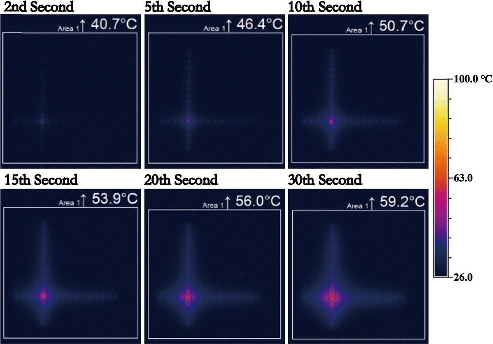 | ||
| Fig. 4 The modulation heating crosstalk phenomenon of the SACNT–paraffin wax composite structure array becomes increasingly more severe with the accumulation of heating cycles in the infrared thermal images at different times. | ||
As the modulation heating time accumulates, the highest temperature at the grid points near the target grid point gradually increases with the number of heating cycles within a single period. With the extension of the heating time, the temperature of the surrounding grids also increases progressively. Consequently, the temperature of the paraffin wax on the grid points in the vicinity of the target one is also heated by the SACNT film, reaching the melting point and causing the paraffin wax in these areas to melt. Due to the short cooling time, the grid points with significant electrical interference on the sample did not have sufficient time to dissipate heat and cool down to room temperature. As intermittent heating continued, heat accumulated over time, leading to a gradual increase in temperature at these points. This observation also helps to explain the phenomenon depicted in Fig. S9 (ESI†), where the paraffin wax on the target grid and its surrounding grids became thinner with the accumulation of heating time. The continuous heating and cooling cycles, along with the heat accumulation due to insufficient cooling, lead to a gradual thinning of the paraffin wax layer, which is a critical factor in the operation and longevity of the SACNT–paraffin wax composite structure.
Due to the fact that the circuit network is prepared using screen printing technology, there are common electrical interference and thermal interference in this process, and there are many ways which could be achieved in the future research of our research group to mitigate these two issues. The most commonly used methods are (1) optimizing the circuit layout, such as increasing the line spacing; (2) using electrode materials with higher conductivity; (3) using thinner transparent insulation or high thermal conductivity substrate materials to enhance the heat dissipation performance of the entire array; (4) a more complex manufacturing process can be used to make diodes on the circuits that block current from other directions; (5) multiple thin layer printing can be used instead of a single thick layer to reduce unevenness, ensure screen alignment accuracy, avoid wire edge burrs, and reduce parasitic capacitance or inductance.
2.8. A spatial light modulation prototype made of the SACNT–paraffin wax composite array
A convenient passive addressing method was employed to actuate the SACNT–paraffin wax array. The spatial light modulation was examined using the following experiment configuration: the array was uniformly illuminated, and after passing through the frosted glass light guide plate, the resulting image was captured with a digital camera. The English letters ‘THU’ were selected to demonstrate the spatial light modulation effect. The display effect of these three letters is depicted in Fig. 5a, where the letters ‘THU’ were clearly discernible. Comparison of the spatial light modulation effect, which is due to the modulated melting of the paraffin wax, is shown in Fig. 5a, with the infrared thermal image presented in Fig. 5b. It is evident that while the crosstalk phenomenon was pronounced in the infrared thermal image, it is considerably mitigated during spatial light modulation. | ||
| Fig. 5 The spatial light modulation effect and infrared thermal image. (a) Spatial light modulation effect of the three letters THU. (b) The corresponding infrared thermal images. | ||
3. Conclusions and outlook
A spatial light modulator fabricated with a SACNT–paraffin wax addressable array that operates using a phase change mechanism is reported. Leveraging the rapid electrical modulation capability, the temperature of the SACNT film can be rapidly altered, which in turn modulates the transmittance of the SACNT–paraffin wax composite structure. Upon powering, the paraffin wax melts as the SACNT film heats at the corresponding grid point of the array. This transition causes the low transmittance of the solid-state paraffin wax to shift to a high transmittance in its melted state, enabling rapid and effective spatial light modulation. The SACNT–paraffin wax system excels with a broad transmission range and no restrictions on the polarization of the light source, offering advantages over the liquid crystal-based devices. This research not only offers new possibilities for thermal radiation control applications, but also expands the application field for the SACNT film. Furthermore, it introduces a novel approach for phase-transition and spatial light modulation.Author contributions
Conceptualization: Liwen Lai and Peng Liu; methodology: Liwen Lai, Peng Liu, Chunhai Zhang and Duanliang Zhou; investigation: Liwen Lai, Peng Liu and Qunqing Li; writing – original draft: Liwen Lai; writing – review & editing: Peng Liu; funding acquisition: Qunqing Li, Peng Liu; resources: Qunqing Li, Peng Liu and Shoushan Fan; supervision: Qunqing Li, Peng Liu and Shoushan Fan.Data availability
The data that support the findings of this study are included in the main text and the ESI.† More data are available from the corresponding author upon reasonable request. Requests for further information, resources, and reagents should be directed to and will be fulfilled by the lead contact, Peng Liu.Conflicts of interest
The authors declare no conflicts of interest.Acknowledgements
The authors thank Dr Lina Zhang, Dr Lin Zhu and Zi Yuan for their help with sample preparation and characterization. This work was financially supported by the National Key Research and Development Program of China (2024YFA1210601 and 2018YFA0208400) and the National Natural Science Foundation of China (NSFC) (No. 51788104, 51727805 and 51532008).References
- X. Zhang, K. Jiang, C. Feng, P. Liu, L. Zhang, J. Kong, T. Zhang, Q. Li and S. Fan, Adv. Mater., 2006, 18(12), 1505–1510 CrossRef CAS.
- K. Jiang, J. Wang, Q. Li, L. Liu, C. Liu and S. Fan, Adv. Mater., 2011, 23(9), 1154–1161 CrossRef CAS PubMed.
- K. Liu, Y. Sun, P. Liu, X. Lin, S. Fan and K. Jiang, Adv. Funct. Mater., 2011, 21(14), 2721–2728 CrossRef CAS.
- C. Feng, K. Liu, J. S. Wu, L. Liu, J. S. Cheng, Y. Zhang, Y. Sun, Q. Li, S. Fan and K. Jiang, Adv. Funct. Mater., 2010, 20(6), 885–891 CrossRef CAS.
- L. Xiao, Y. Zhang, Y. Wang, K. Liu, Z. Wang, T. Li, Z. Jiang, J. Shi, L. Liu, Q. Li, Y. Zhao, Z. Feng, S. Fan and K. Jiang, Nanotechnology, 2011, 22, 025502 CrossRef PubMed.
- L. Cong, Z. Yuan, Z. Bai, X. Wang, W. Zhao, X. Gao, X. Hu, P. Liu, W. Guo, Q. Li, S. Fan and K. Jiang, Sci. Adv., 2021, 7(12), eabd2358 CrossRef CAS PubMed.
- Y. Jin, T. Zhang, Z. Huang, J. Zhao, Y. Zhao, Z. Wang, L. Lai, J. Wang, K. Jiang, S. Fan and Q. Li, Carbon, 2020, 161, 510–516 CrossRef CAS.
- Z. Wang, L. Lai, T. Zhang, S. Wu, J. Zhao, Y. Zhao, Y. Jin, J. Wang, S. Fan and Q. Li, ACS Appl. Energy Mater., 2021, 4(10), 10542–10552 CrossRef CAS.
- Z. Wang, L. Lai, Y. Wang, T. Zhang, Z. Huang, Y. Jin, J. Wang, K. Jiang, S. Fan and Q. Li, Int. J. Hydrogen Energy, 2020, 45(56), 31963–31975 CrossRef CAS.
- Y. Jin, Q. Li, M. Chen, G. Li, Y. Zhao, X. Xiao, J. Wang, K. Jiang and S. Fan, Nanoscale, 2015, 7(39), 16508–16515 RSC.
- L. Lai, P. Liu, D. Zhou, Q. Li, S. Fan and W. Lu, Adv. Funct. Mater., 2022, 33(4), 2208891 CrossRef.
- W. Zhang, M. Weng, P. Zhou, L. Chen, Z. Huang, L. Zhang, C. Liu and S. Fan, Carbon, 2017, 116, 625–632 CrossRef CAS.
- L. Xiao, Z. Chen, C. Feng, L. Liu, Z.-Q. Bai, Y. Wang, L. Qian, Y. Zhang, Q. Li, K. Jiang and S. Fan, Nano Lett., 2012, 8(12), 4539–4545 CrossRef PubMed.
- P. Liu, L. Liu, Y. Wei, K. Liu, Z. Chen, K. Jiang, Q. Li and S. Fan, Adv. Mater., 2009, 21(35), 3563–3566 CrossRef CAS.
- Y. Wei, P. Liu, K. Jiang and S. Fan, Nano Lett., 2012, 12(5), 2548–2553 CrossRef CAS PubMed.
- P. Liu, D. Zhou, Y. Wei, K. Jiang, J. Wang, L. Zhang, Q. Li and S. Fan, ACS Nano, 2015, 9(4), 3753–3759 CrossRef CAS PubMed.
- W. Ning, Z. Wang, P. Liu, D. Zhou, S. Yang, J. Wang, Q. Li, S. Fan and K. Jiang, Carbon, 2018, 139, 1136–1143 CrossRef CAS.
- L. Xiao, H. Ma, J. Liu, W. Zhao, Y. Jia, Q. Zhao, K. Liu, Y. Wu, Y. Wei, S. Fan and K. Jiang, Nano Lett., 2015, 15(12), 8365–8370 CrossRef CAS PubMed.
- W. Yu, C. Liu and S. Fan, Nano Res., 2021, 14(8), 2471–2490 CrossRef.
- A. Farzanehnia, M. Khatibi, M. Sardarabadi and M. Passandideh-Fard, Energy Convers. Manage., 2019, 179, 314–325 CrossRef CAS.
- D. Xu, C. Gao, Y. Liu, C. Ge, Y. Wei, Z. Peng, K. Liu, Y. Hong, W. Xu and J. Fang, Device, 2024, 2(8), 100366 CrossRef.
- C. Xiao, B. Liao and E. W. Hawkes, Device, 2024, 2(1), 100186 CrossRef.
- Y. Li and X. Chen, Device, 2024, 2(2), 100282 CrossRef.
- P. Liu, L. Liu, K. Jiang and S. Fan, Small, 2011, 7(6), 732–736 CrossRef CAS PubMed.
- P. Zhou, W. Zhang, L. Chen, J. Lin, Z. Luo, C. Liu and K. Jiang, Nano Res., 2021, 14(7), 2456–2462 CrossRef CAS.
- G. Kim, S. Kim, H. Kim, J. Lee, T. Badloe and J. Rho, Nanoscale, 2022, 14(12), 4380–4410 RSC.
- A. Weiss, C. Frydendahl, J. Bar-David, R. Zektzer, E. Edrei, J. Engelberg, N. Mazurski, B. Desiatov and U. Levy, ACS Photonics, 2022, 9(2), 605–612 CrossRef CAS.
- J. Park, B. G. Jeong, S. I. Kim, D. Lee, J. Kim, C. Shin, C. B. Lee, T. Otsuka, J. Kyoung, S. Kim, K.-Y. Yang, Y.-Y. Park, J. Lee, I. Hwang, J. Jang, S. H. Song, M. L. Brongersma, K. Ha, S.-W. Hwang, H. Choo and B. L. Choi, Nat. Nanotechnol., 2020, 16(1), 69–76 CrossRef PubMed.
- A. H. Dorrah and F. Capasso, Science, 2022, 376(6591), eabi6860 CrossRef CAS PubMed.
- S. Pirotta, N.-L. Tran, A. Jollivet, G. Biasiol, P. Crozat, J.-M. Manceau, A. Bousseksou and R. Colombelli, Nat. Commun., 2021, 12(1), 799 CrossRef CAS PubMed.
- H. M. L. Robert, K. Holanová, Ł. Bujak, M. Vala, V. Henrichs, Z. Lánský and M. Piliarik, Nat. Commun., 2021, 12(1), 2921 CrossRef CAS PubMed.
- G.-B. Wu, J. Y. Dai, Q. Cheng, T. J. Cui and C. H. Chan, Nat. Electron., 2022, 5(11), 808–819 CrossRef.
- C. L. Panuski, I. Christen, M. Minkov, C. J. Brabec, S. Trajtenberg-Mills, A. D. Griffiths, J. J. McKendry, G. L. Leake, D. J. Coleman and C. Tran, Nat. Photonics, 2022, 16(12), 834–842 CrossRef CAS.
- V. Gurses, Nat. Photonics, 2022, 16(12), 818–820 CrossRef CAS.
- J. Wu, Z. Shen, S. Ge, B. Chen, Z. Shen, T. Wang, C. Zhang, W. Hu, K. Fan, W. Padilla, Y. Lu, B. Jin, J. Chen and P. Wu, Appl. Phys. Lett., 2020, 116(13), 131104 CrossRef CAS.
- A. S. Ostrovsky, C. Rickenstorff-Parrao and V. Arrizón, Opt. Lett., 2013, 38(4), 534–536 CrossRef PubMed.
- B. Liu and H.-M. Cheng, Nat. Nanotechnol., 2022, 17(10), 1050–1051 CrossRef PubMed.
- M. Klein, R. Binder, M. R. Koehler, D. G. Mandrus, T. Taniguchi, K. Watanabe and J. R. Schaibley, Nat. Commun., 2022, 13(1), 6216 CrossRef CAS PubMed.
- C. Cen, Y. Zhang, X. Chen, H. Yang, Z. Yi, W. Yao, Y. Tang, Y. Yi, J. Wang and P. Wu, Phys. E, 2020, 117, 113840 CrossRef CAS.
- S.-Q. Li, X. Xu, R. Maruthiyodan Veetil, V. Valuckas, R. Paniagua-Domínguez and A. I. Kuznetsov, Science, 2019, 364(40), 1087–1090 CrossRef CAS PubMed.
- H. Zheng, Q. Liu, Y. Zhou, I. I. Kravchenko, Y. Huo and J. Valentine, Sci. Adv., 2022, 8(30), eabo6410 CrossRef PubMed.
- H. Kwon, T. Zheng and A. Faraon, Nat. Commun., 2022, 13(1), 5811 CrossRef CAS PubMed.
- A. Leitis, A. Heßler, S. Wahl, M. Wuttig, T. Taubner, A. Tittl and H. Altug, Adv. Funct. Mater., 2020, 30(19), 1910259 CrossRef CAS.
- Y. Zhang, J. B. Chou, J. Li, H. Li, Q. Du, A. Yadav, S. Zhou, M. Y. Shalaginov, Z. Fang, H. Zhong, C. Roberts, P. Robinson, B. Bohlin, C. Ríos, H. Lin, M. Kang, T. Gu, J. Warner, V. Liberman, K. Richardson and J. Hu, Nat. Commun., 2019, 10(1), 4279 CrossRef PubMed.
- A. B. Ayoub and D. Psaltis, Sci. Rep., 2021, 11(1), 18837 CrossRef CAS PubMed.
- P. Zhang, B. Fang, T. Zhao, L. Ke, X. Ma, C. Li, Z. Hong and X. Jing, Results Phys., 2023, 46, 106328 CrossRef.
- H. Ahmed, H. Kim, Y. Zhang, Y. Intaravanne, J. Jang, J. Rho, S. Chen and X. Chen, Nanophotonics, 2022, 11(5), 941–956 CrossRef CAS PubMed.
- Z. Ba and X. Wang A Transmission Metasurface for Generating High-efficiency Broadband Millimeter Wave OAM Beams, 2019 13th European Conference on Antennas and Propagation (EuCAP), 2019.
- M. Pivnenko, K. Li and D. Chu, Opt. Express, 2021, 29(16), 24614–24628 CrossRef CAS PubMed.
- J. Qian, B. Li, S. Tian, B. Liu and X. Zhao, Appl. Surf. Sci., 2022, 605, 154680 CrossRef CAS.
- J. Outón, A. Casas-Acuña, M. Domínguez, E. Blanco, J. J. Delgado and M. Ramírez-del-Solar, Appl. Surf. Sci., 2023, 608, 155180 CrossRef.
- J. Liu, R. Yang, J. Zhang, Q. Tao, A. Li, Z. Liu, Y. Su and Y. Liu, Solar Energy Mater. Solar Cells, 2023, 249, 112048 CrossRef CAS.
- L. Wang, J. Wang, Y. Wang and X. Zhang, React. Funct. Poly., 2022, 181, 105408 CrossRef CAS.
- P. Li, Z. Sun, R. Wang, Y. Gong, Y. Zhou, Y. Wang, X. Liu, X. Zhou, J. Ouyang, M. Chen, C. Hou, M. Chen and G. Tao, Front. Optoelectron., 2022, 15, 40 CrossRef PubMed.
- Y. Guo, L. Zhu, S. Chen, S. Zhou, Q. Pan, J. Zhao and Y. Shuai, Appl. Phys. Lett., 2022, 121(20), 201102 CrossRef CAS.
- P. Schofield, A. Bradicich, R. M. Gurrola, Y. Zhang, T. D. Brown, M. Pharr, P. J. Shamberger and S. Banerjee, Adv. Mater., 2022, 35(37), 2205294 CrossRef PubMed.
Footnote |
| † Electronic supplementary information (ESI) available. See DOI: https://doi.org/10.1039/d5nh00007f |
| This journal is © The Royal Society of Chemistry 2025 |