
Granular memristors with tunable stochasticity†
Uddipan
Ghosh
 ,
Ankur
Bhaumik
,
Navyashree
Vasudeva
and
Anshu
Pandey
*
,
Ankur
Bhaumik
,
Navyashree
Vasudeva
and
Anshu
Pandey
*
Solid State and Structural Chemistry Unit, Indian Institute of Science, Bangalore, Karnataka-560012, India. E-mail: anshup@iisc.ac.in
First published on 2nd December 2024
Abstract
Most realizations of memristive devices exhibit characteristic noise sometimes described as random telegraph noise. These fluctuations in current, ubiquitous in nature, carry significant implications for device performance, reliability, and the broader landscape of memristor technology applications. Here, we study inherent random fluctuations observed in silver based granular memristive devices operating under steady bias conditions. Random telegraph noise observed in our system is characterized in terms of distributions of ON and OFF times of the current flow at a particular bias. We find that these fluctuations adhere to power law statistics with  , where τOFF/ON denotes the time during which the output value remains below or above a specified threshold. We follow the fluctuations for up to four decades. Significantly, unlike previous studies, we find the emergence of a new regime of behavior where the power law exponent varies as a function of applied bias. We find that our results are best described by the Marcus–Tang expression for diffusion along intersecting parabolae with bias as the driving force. The predictions of this picture of dynamics also provide a satisfactory explanation for the quiescence of the OFF/ON state of our devices.
Introduction
The memristor, initially proposed by Dr Leon Chua in 1971,1 became a physical reality through the pioneering work of HP research laboratories in 2008,2 representing a critical connection between magnetic flux and charge. The conductance level at a specified voltage stands out as a pivotal parameter dictating the inherent stability of these devices. However, fluctuations in device resistance pose a substantial challenge to their efficiency in deterministic memory devices.3,4 Investigating the nature of these random fluctuations inherent to memristors is essential for understanding their mechanistic intricacies and offers avenues for effective modulation, ultimately impacting device performance. Such stochasticity is more prominent in those memristive devices where the switching happens through the migration of metal ions inside an insulator matrix.5Models to describe memristive behavior can be categorized into four broad types:dynamical, microstructural, thermodynamic and stochastic.6–12 Wei Lu et al. showed that the two-level random telegraph noise (RTN) from the high resistance state (HRS) of a Resistive Random Access Memory (RRAM) device made of Pd/TaO2/Pd results from variable range hopping between oxygen vacancy centres.13 Botond et al. have shown that the current-to-noise ratio universally depends on the total resistance of the device. They have also shown that upon changing the conduction mode from diffusion to ballistic, the dependence of noise upon the resistance of the device changes significantly.14
Despite the interest of the scientific community in this attribute of memristors, pressing questions regarding this noise remain. For example, it remains unclear if diffusive processes in memristive devices are universal across device platforms or else specific to certain device architectures and regimes. Furthermore, the long range temporal correlation in the conductance value at a fixed voltage15,16 that is typically observed is yet to be properly understood. Similarly, the reasons for differences between characteristic fluctuations in the low resistance state (LRS) and HRS remain unclear.
Here, we describe intriguing current-flow behavior in a granular Ag-based memristor with AgBr as the dielectric. Similar to previous studies of silver based memristors, we observe that the current in the system exhibits random fluctuations over time, with detailed analysis revealing stepwise changes. These steps are attributed to the formation and breaking of conducting weak links within the granular material, driven by the interconversion of Ag and Ag+ in the medium. It is found that the information entropy associated with the current flow lies in the range of 0.2–0.8 over all measurements, consistent with correlations between the seemingly stochastic fluctuations. The OFF and ON state time distribution probabilities of the LRS follow power law

Results and discussion
Although memristors can have several underlying architectures, most solid state memristor devices rely upon field induced changes in the conductivity of an insulator layer. This is typically accomplished either through electrochemical control of the redox state or else through the field induced diffusion of a conductive component into the insulator, or alternately both.20,23,21,22 The insulator thus simultaneously affects the LRS/HRS resistance as well as the switching bias of the devices. Several recently investigated devices rely on the diffusion of silver ions through a host insulator layer. Silver based devices have gained in prominence due to the large diffusion constants of silver ions as well as the redox activity of silver that enables reversible device switching within a convenient working range. Most silver-based devices investigated to date rely on a monolithic architecture where a single homogeneous insulator layer is placed between electrical contacts. In our work, we look to extend this architecture by introducing a scaffold of conductive nanoparticles into the insulating AgBr matrix, leading to a granular memristive architecture. We thus employ granular AgBr grown onto Au nanoparticles (NPs) ranging from 20 to 30 nm in size as our working material. This material was synthesized by initially starting from the gold scaffold, that is, gold NPs. Silver bromide is subsequently grown over these NPs through precipitation. Initially, the gold scaffold is synthesized by reducing gold chloride salt with sodium borohydride, using cetyl-trimethylammonium bromide (CTAB) as a ligand, resulting in gold nanoparticles of approximately 1–2 nm size. These nanoparticles are further enlarged to 20–30 nm by placing them in a growth medium containing CTAB, ascorbic acid, and HAuCl4.24 Following this, Au NPs in CTAB solution are treated with silver nitrate in the presence of light and the reaction is left undisturbed for 24 hours. This step facilitates the gradual deposition of an AgBr layer on the surface of the gold nanospheres. Bromide ions are derived from the CTAB present in the medium. This transformation creates a conductive scaffold embedded within an electrochemically active layer, thereby establishing the matrix integral to the memristive device's functionality.For characterization, a thin film of the synthesized material was deposited onto a glass substrate, and its crystallographic properties were analyzed using X-ray diffraction (XRD). Fig. 1a shows the XRD pattern of the sample along with standard diffraction patterns of Ag metal and AgBr in its face-centred cubic (fcc) form. The analysis revealed distinct diffraction maxima corresponding to the crystallographic planes of silver and gold. Specifically, the observed peaks are seen to agree well with the (111), (200), (220), and (311) planes of these metals. The presence of these peaks indicates the successful incorporation of both silver and gold in the sample. A particularly noteworthy feature in the XRD pattern was the intense peak corresponding to the (200) plane of silver bromide. The observation of this peak is significant as it validates the coexistence of Ag and AgBr within the insulator layer.
 | ||
| Fig. 1 (a) XRD of the insulator layer; (b) SEM of the insulator layer; and (c–e) XPS spectra of Ag, Au and Br, respectively. | ||
Scanning electron microscopy reveals particles approximately 250 nm in size, as seen in Fig. 1b, confirming the granular morphology of the synthesized material (additional microscopy data can be found in ESI Fig. S1 and S2†). X-ray photoelectron spectroscopy (XPS) was employed to confirm the coexistence of Ag, Ag+, Au and Br−. The presence of 3d5/2 of metallic Ag and Ag+ at 366.87 eV and 367.57 eV, respectively, along with Br 3d5/2 and 3d3/2 at 67.28 eV and 68.33 eV, and Au 4f7/2 and 4f5/2 at 83.12 eV and 86.90 eV, respectively, confirms the presence of these elements in the synthesized sample (Fig. 1c–e).25,26
Electrical properties were measured by casting the material between two patterned Au electrodes 200 μm apart. The gap was kept at 200 μm to prevent shorting during long measurements. Devices with larger gaps were inconvenient as they are more resistive in nature. The film was subsequently heated to 60 °C to facilitate drying. The thickness of the dropcast layer was found to be 2 μm in cross-sectional SEM. The 2 μm thickness ensures continuity of the film. The top view of the device is presented in the inset of Fig. 2a. A cross-sectional view is also shown in Fig. 2b. The patterned electrode was fabricated on the glass substrate by evaporating 15 nm chromium at the bottom and depositing 150 nm of gold on top (the SEM of the device is shown in Fig. S3a of the ESI†). Electrical measurements were conducted by applying different voltages to the sample, and the resulting current values were recorded. All the measurements were done in a two-probe geometry (a schematic of the measurement setup is shown in ESI Fig. S4†).
 | ||
| Fig. 2 (a) Cross-sectional SEM of the device (inset: schematic top view of the device); (b) cross-sectional schematic of the device; and (c) current–voltage characteristics of the device. | ||
The current–voltage characteristics yield a typical pinched hysteresis loop of a memristive device27,28 (Fig. 2c). The device sets and resets at (2.8 V, −3.95 V) and (0.5 V, −0.6 V) for both positive and negative bias, respectively. A large switching ratio ROFF/RON of 1.2 × 10⁵ is observed in this particular example (variation of ROFF and RON over cycles, devices and batches is shown in ESI Fig. S10†). The underlying chemical mechanisms governing silver based memristive devices have been reported previously.29 Upon applying a bias across electrodes, Ag metal oxidizes and the resulting silver ions diffuse towards the metal contact at a lower potential. Here, these are reduced to form a bridge between the metal contacts (UV-vis and Raman spectra showing diminished silver halide feature in the LRS are presented in ESI Fig. S9†). In our system, adjacent Au NPs provide additional metallic contacts for this process besides the electrodes themselves. These metallic links connect at the set voltage, forming a continuous ohmic connection between the two contacts. The material achieves heightened conductivity at this juncture, representing the onset of its LRS. Conversely, upon application of the reset voltage, applied in the reverse direction to the set voltage, Ag diffuses in the back direction. This transformation leads to a loss of conductivity, returning the material to its HRS (a schematic of the device in the LRS and HRS is presented in ESI Fig. S3b†).
Our main interest in this work is to study the physical aspects of mechanisms occurring in these systems. For this purpose, we turn to studying the properties of the device in the LRS and HRS. To study the device's properties in its LRS, current variation with time was recorded for 16![[thin space (1/6-em)]](https://www.rsc.org/images/entities/char_2009.gif) 000 seconds at a fixed 1 V bias (Fig. 3a). We observed random fluctuations of current over time on three different time scales. Fig. 3b shows an expanded view of the data recorded in the shaded region of Fig. 3a. Likewise, Fig. 3c shows an expanded view of the data shown in Fig. 3b. As evident from these panels, the current fluctuations occur over all timescales considered here, consistent with other recent reports on memristors.13,14 In contrast to the fluctuations observed in the LRS, we observe that the device HRS is stable (Fig. 3d). More interestingly, we find that in certain events, the current observed in the LRS falls to values associated with the HRS before reverting back to its usual range. In contrast, the HRS does not appear to visit the LRS over the measured time intervals. To check the randomness of these fluctuations, the information content of the dataset was estimated using Shannon's information entropy,
000 seconds at a fixed 1 V bias (Fig. 3a). We observed random fluctuations of current over time on three different time scales. Fig. 3b shows an expanded view of the data recorded in the shaded region of Fig. 3a. Likewise, Fig. 3c shows an expanded view of the data shown in Fig. 3b. As evident from these panels, the current fluctuations occur over all timescales considered here, consistent with other recent reports on memristors.13,14 In contrast to the fluctuations observed in the LRS, we observe that the device HRS is stable (Fig. 3d). More interestingly, we find that in certain events, the current observed in the LRS falls to values associated with the HRS before reverting back to its usual range. In contrast, the HRS does not appear to visit the LRS over the measured time intervals. To check the randomness of these fluctuations, the information content of the dataset was estimated using Shannon's information entropy,
 000 points. Then, a bin-wise Fourier transform was employed to extract the fluctuation frequency. Amplitudes of the observed frequencies were then employed to obtain information entropy. The information entropy content of the signal shown is shown in Fig. 3e. We found an average value of 0.51 ± 0.1. Sub-unity information entropy associated with this signal implies that the fluctuations are correlated, thus justifying our later treatment. The Fourier transform of the observed signal fits well to an exponent of 1.5 (Fig. 3f) that differs significantly from the instrument noise that shows an exponent of 0.98 (Fig. S5 in the ESI†).
 | ||
| Fig. 3 (a–c) Variation of current over three different time ranges during the LRS taken at fixed 1 V bias; (d) fluctuation of current over time at the HRS at 1 V bias; (e) information entropy derived from a; and (f) Fourier transform of a. | ||
To understand fluctuation correlations in the time domain, the measured signal was digitized into ON and OFF and binned based on observational probabilities associated with ON and OFF times. This is similar to previous reports.30,31 To implement this binning, a threshold was defined based on the mean of all the current values recorded (the choice of threshold is discussed in ESI Fig. S6†). Currents exceeding the threshold are ascribed to an “ON” state and those below the threshold to an “OFF” state (Fig. 4a). The duration τON is defined as the duration for which the device current stays above the threshold before switching to its OFF state. Similarly, τOFF is the duration for which the device current stays below the threshold current before switching to its ON state. Switching of the system between its ON and OFF current values while in its LRS leads to a distribution of ON/OFF times P(τON/OFF). Here, P(τON/OFF) corresponds to the probability of occurrence of a lifetime τON/OFF. As shown in Fig. 4b and c, at 1 V bias, P(τON/OFF) fits well to a power law P(τON/OFF) = 10kτON/OFF−α. The distribution of ON and OFF times follows a power law for four decades on the x axis and five decades on the y axis. This is similar to earlier studies on stochastic memristive systems that were shown to follow power law behavior for 2–3 decades for the x and y axes, respectively.30,31 We found α(OFF) = 1.27 and α(ON) = 1.14. While these data were recorded at 1 V bias, we found that α(ON/OFF) increases with applied bias. This is shown in Fig. 4d–f. Fig. 4d and e in particular show that at a 9 V bias, α(OFF) = 1.52 and α(ON) = 1.64. Fig. 4f shows the systematic evolution of α(ON/OFF) as a function of applied bias (current vs. time data and power law plots of other biases are plotted in ESI Fig. S7 and S8, respectively†). We note that bias dependence of α has not been observed previously in silver based memristors and appears unique to our system.
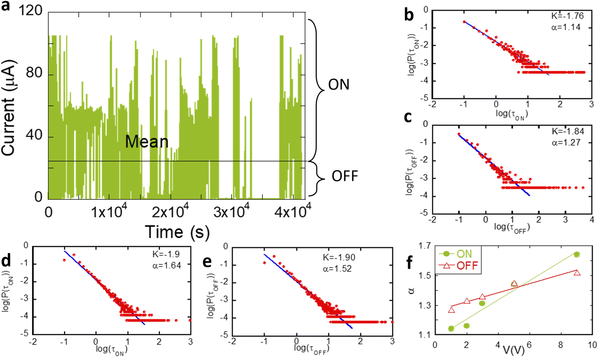 | ||
| Fig. 4 (a) Variation of current at 1 V at the LRS; (b and c) power law analysis of ON and OFF times, respectively, at 1 V; (d and e) power law analysis of ON and OFF times at 9 V, respectively; and (f) variation of α with bias voltage. | ||
To better understand this, we examined the applicability of driven diffusion models of system free energy. The Marcus–Tang theory of system diffusion along parabolic free energy surfaces is especially significant and has been applied with great success to problems of quantum dot blinking.19 Given the qualitative similarity of our observations to quantum dot blinking and the granular character of our system, we turned to examine the applicability of this model to our observations.
Marcus–Tang theory associates parabolic free energy surfaces with two states of interest. In the context of quantum dots, these parabolae represent emissive and non-emissive excited states of the system. The system transitions between emissive and non-emissive states by diffusing from one free energy surface into another at the point of intersection of the two parabolae. This leads to an expression for system migration between ON and OFF states.

The power law exponent arising from this process is typically close to 1.5 that is remarkably similar to the observed α(OFF) = 1.52 and α(ON) = 1.64 at 9 V bias. Diffusion along parabolic coordinates thus presents an accurate picture of memristor behavior at elevated bias. In our case, since the two states are associated with a high and low resistance, these likely arise from the preponderance of Ag+ (OFF/high resistance) and Ag (ON/low resistance) in the current carrying path. This interpretation is consistent with previous interpretations of Ag based memristor devices where the presence of Ag along the current carrying path is found to lead to a lower device resistance. Thus the Ag+ and Ag rich states of the device can be associated with the two parabolic free energy surfaces U1 and U2 (Fig. 5a). The crossover between these two surfaces is shown in Fig. 5a where the y axis indicates the free energy G and the x axis indicates the reaction coordinate Q. Here, Q1 and Q2 are minima of Ag+ and Ag free energy surfaces, respectively, crossing at Qc. The activation barrier for state crossing is ΔG‡ and the free energy difference between the two states is ΔG°. Diffusion of the system along the Ag+ free energy surface to the Ag surface will be reflected as an ON event and the reverse as an OFF event. The parabolae are given by the following equations:
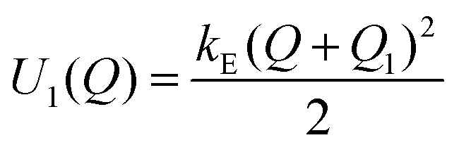 | (1) |
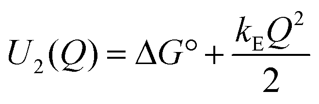 | (2) |

 | ||
| Fig. 5 (a) Free energy diagram of the system; and (b and c) free energy diagram at the HRS and LRS, respectively. | ||
The energy of Qc serves as a bottleneck to the state switching process. The rate of change of population at the Ag+ and Ag surface due to the diffusion of electrons from Ag+ to Ag and vice versa can be represented taking Q2 as the origin via a non-adiabatic electron transfer equation. Marcus and Tang solved this to obtain
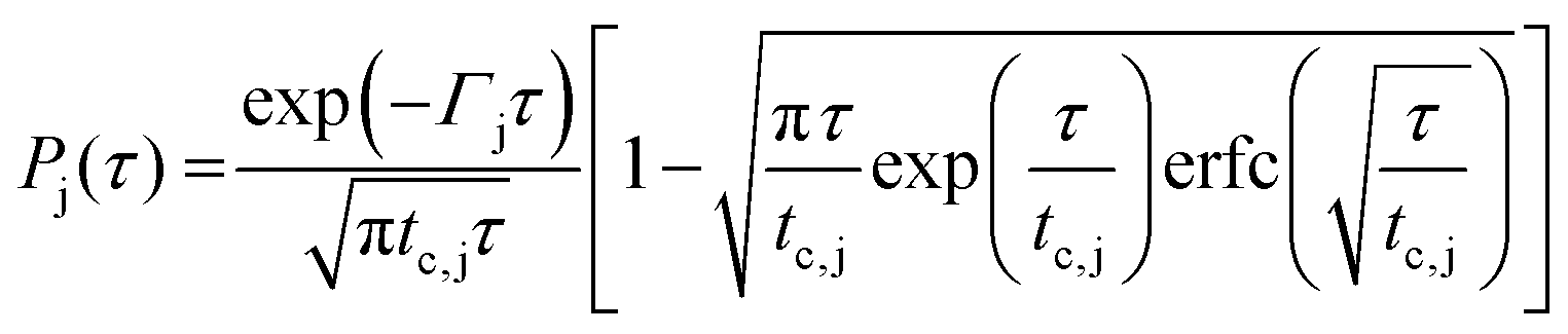
 and
and  . This equation can be further reduced to the form of a fitting equation by considering the time regime, τOFF/ON ≫ tc,j.
The MT model also suggests a physical picture of the mechanism by which bias driven system diffusion occurs. Based on the above model, the application of a bias drives a current through the system. This causes the conversion of Ag+ into Ag and vice versa in the system due to the accumulation and removal of electrons within the system. Thus, at higher bias, increased current flow through the system causes more diffusion along the system coordinates, leading the MT mechanism to become more prominent. This is manifested as better agreement of the observed α with the MT estimate of the exponent. We have listed the MT fitting parameters for the 9 V data in Table 1.
| State | k | α |
|---|---|---|
| OFF | −1.9 | 1.64 |
| ON | −1.9 | 1.52 |
It is worth noting that in the case of quantum dots, the driver for the diffusion process is not clear as changing parameters like temperature and light intensity does not change the power law exponent. But in our case, change of the exponent with changing bias is significant and thus establishes bias or current flowing through the device to be the sole driver of the diffusion process. When the device is biased at lower voltages, other factors like charge trapping–detrapping and quantum transport predominately cause fluctuations in the current level. However, at higher voltages, MT processes take over.
A more significant outcome of applicability of the MT model is that it naturally predicts the occurrence of ON/OFF noise in the LRS of the system along with the absence of noise in the HRS. To see this, we first consider the MT picture for the system HRS and LRS. These are shown in Fig. 5b and c. As shown here, the HRS corresponds to a situation where the more resistive (Ag+ rich) phase is thermodynamically stable and therefore more abundant in the system. Likewise, the application of an appropriate bias causes a chemical transformation whereby the less resistive (Ag rich) phase becomes more abundant. From Fig. 5b and c, it is evident that the crossing point from the low free energy phase to the higher free energy phase is associated with a high activation energy (ΔG‡). In contrast, the activation energy associated with crossing from the higher free energy phase to the lower free energy phase is lower (ΔG‡ − ΔG°). The difference in activation energies has important consequences for the stability of the HRS and LRS of the system. The HRS configuration is shown in Fig. 5b. Here, the Ag+ paraboloid represents the lowest free energy configuration. Furthermore, since the current flow in the system in this configuration is restricted, the system tends to remain confined to the ground state paraboloid. This leads the system HRS to exhibit remarkable stability. The situation is reversed in the case where the LRS is more stable. Here, there is increased current flow through the system that provides a sufficient driving force for crossing over from the Ag paraboloid (ON state) to the less conductive Ag+ paraboloid (OFF state). In the OFF state, even though the current flow is decreased, the system is nonetheless able to diffuse back to the Ag paraboloid since the backwards diffusion is associated with a significantly lower activation energy (Fig. 5b). Thus, the Marcus–Tang model correctly predicts the stability of the HRS, along with the tendency of the LRS to switch between ON and OFF configurations.
Conclusions
In conclusion, our study delves into the dynamic behavior of a silver-based memristor under constant voltage bias, revealing intriguing insights into its fluctuation characteristics. The observed random fluctuations, analyzed through statistical methods, demonstrate stepwise changes in current values attributed to the formation and breaking of conducting weak links within the granular material. These fluctuations, showcasing a power-law behavior, are reminiscent of quantum dot blinking studies and are explained using the MT theory of diffusion-controlled electron transfer. The proposed model, incorporating free energy parabolas associated with Ag-rich and Ag+ rich states, successfully describes the power-law statistics observed in ‘ON’ and ‘OFF’ events. Experimental data, fitting well to the proposed equations, show that the observed exponent values align with theoretical predictions. Notably, increasing bias voltage correlates with higher exponent values, emphasizing the influence of external parameters on the observed power-law behavior. This tunability enables potential applications such as encryption, and neuromorphic and probabilistic computing.32–40 This comprehensive investigation not only advances our understanding of memristor operation mechanisms but also underscores the potential applicability of established theories from related fields to memristor behavior.Author contributions
UG and AP conceived the idea. UG did material synthesis, device fabrication, characterization and analysis. AB wrote codes to acquire and analyze data. NV synthesized and characterized Au NS. UG and AP wrote the manuscript with inputs from other authors.Data availability
The data that support the findings of this study are available from the corresponding author upon reasonable request.Conflicts of interest
The authors share no conflict of interest.Acknowledgements
AP acknowledges Indian Institute of Science and DST SERB IRHPA [IPA/2020/000033] for the support. UG acknowledges IISc for funding. UG and AP acknowledge Prof. Sushobhan Avasthi and Prof. Pavan Nukala for useful discussions. UG acknowledges the Horiba- IISc Technical Centre for Raman measurements.References
- L. Chua, IEEE Trans. Circuit Theory, 1971, 18, 507–519 Search PubMed.
- D. B. Strukov, G. S. Snider, D. R. Stewart and R. S. Williams, Nature, 2008, 453, 80–83 CrossRef CAS PubMed.
- J. J. Yang, D. B. Strukov and D. R. Stewart, Nat. Nanotechnol., 2013, 8, 13–24 CrossRef CAS PubMed.
- K. Humood, S. Saylan, B. Mohammad and M. Abi Jaoude, J. Electron. Mater., 2021, 50, 4397–4406 CrossRef CAS.
- S. H. Jo, K.-H. Kim and W. Lu, Nano Lett., 2009, 9, 496–500 CrossRef CAS PubMed.
- D. Ielmini, IEEE Trans. Electron Devices, 2011, 58, 4309–4317 CAS.
- S. Kim, S. J. Kim, K. M. Kim, S. R. Lee, M. Chang, E. Cho, Y.B. Kim, C. J. Kim, U. In Chung and I. K. Yoo, Sci. Rep., 2013, 3, 1680 CrossRef PubMed.
- V. G. Karpov, D. Niraula, I. V. Karpov and R. Kotlyar, Phys. Rev. Appl., 2017, 8, 24028 CrossRef.
- N. V. Agudov, A. V. Safonov, A. V. Krichigin, A. A. Kharcheva, A. A. Dubkov, D. Valenti, D. V. Guseinov, A. I. Belov, A. N. Mikhaylov, A. Carollo and B. Spagnolo, J. Stat. Mech.: Theory Exp., 2020, 2020, 024003 CrossRef.
- N. V. Agudov, A. A. Dubkov, A. V. Safonov, A. V. Krichigin, A. A. Kharcheva, D. V. Guseinov, M. N. Koryazhkina, A. S. Novikov, V. A. Shishmakova, I. N. Antonov, A. Carollo and B. Spagnolo, Chaos, Solitons Fractals, 2021, 150, 111131 CrossRef.
- E. Linn, A. Siemon, R. Waser and S. Menzel, IEEE Trans. Circuits Syst. I Regul. Pap., 2014, 61, 2402–2410 Search PubMed.
- S. Kim, S. Choi and W. Lu, ACS Nano, 2014, 8, 2369–2376 CrossRef CAS PubMed.
- S. Choi, Y. Yang and W. Lu, Nanoscale, 2014, 6, 400–404 RSC.
- B. Sánta, Z. Balogh, A. Gubicza, L. Pósa, D. Krisztián, G. Mihály, M. Csontos and A. Halbritter, Nanoscale, 2019, 11, 4719–4725 RSC.
- S. Shirai, S. K. Acharya, S. K. Bose, J. B. Mallinson, E. Galli, M. D. Pike, M. D. Arnold and S. A. Brown, Netw. Neurosci., 2020, 4, 432–447 CrossRef PubMed.
- N. Carstens, B. Adejube, T. Strunskus, F. Faupel, S. Brown and A. Vahl, Nanoscale Adv., 2022, 4, 3149–3160 RSC.
- M. Kuno, D. P. Fromm, H. F. Hamann, A. Gallagher and D. J. Nesbitt, J. Chem. Phys., 2001, 115, 1028–1040 CrossRef CAS.
- A. L. Efros and D. J. Nesbitt, Nat. Nanotechnol., 2016, 11, 661–671 CrossRef CAS PubMed.
- J. Tang and R. A. Marcus, J. Chem. Phys., 2005, 123, 054704 CrossRef PubMed.
- I. Valov and M. N. Kozicki, J. Phys. D: Appl. Phys., 2013, 46, 074005 CrossRef CAS.
- Q. Liu, J. Sun, H. Lv, S. Long, K. Yin, N. Wan, Y. Li, L. Sun and M. Liu, Adv. Mater., 2012, 24, 1844–1849 CrossRef CAS PubMed.
- Q. Liu, J. Sun, H. Lv, S. Long, K. Yin, N. Wan, Y. Li, L. Sun and M. Liu, Adv. Mater., 2012, 24, 1844–1849 CrossRef CAS PubMed.
- K. Sun, J. Chen and X. Yan, Adv. Funct. Mater., 2021, 31(8), 2006773 CrossRef CAS.
- N. R. Jana, L. Gearheart and C. J. Murphy, Adv. Mater., 2001, 13, 1389–1393 CrossRef CAS.
- T. Li, Y. Liu, R. Jia, M. Yaseen, L. Shi and L. Huang, New J. Chem., 2021, 45, 22327–22334 RSC.
- V. Kammara, P. Venkataswamy, G. Ravi, K. Ramaswamy, M. Sunku and M. Vithal, Inorg. Chem. Commun., 2022, 141, 109504 CrossRef CAS.
- L. Chua, Semicond. Sci. Technol., 2014, 29, 104001 CrossRef.
- L. Hu, G. T. Lin, X. Luo, R. H. Wei, X. B. Zhu, W. H. Song, J. M. Dai and Y. P. Sun, J. Appl. Phys., 2016, 120(21), 215303 CrossRef.
- Y. Yang, P. Gao, S. Gaba, T. Chang, X. Pan and W. Lu, Nat. Commun., 2012, 3, 732 CrossRef PubMed.
- Z. Ma, W. Chen, X. Cao, S. Diao, Z. Liu, J. Ge and S. Pan, Nano Lett., 2023, 23, 5902–5910 CrossRef CAS PubMed.
- A. Rao, S. Sanjay, V. Dey, M. Ahmadi, P. Yadav, A. Venugopalrao, N. Bhat, B. Kooi, S. Raghavan and P. Nukala, Mater. Horiz., 2023, 10, 5235–5245 RSC.
- K. S. Woo, J. Han, S. Yi, L. Thomas, H. Park, S. Kumar and C. S. Hwang, Nat. Commun., 2024, 15, 3245 CrossRef CAS PubMed.
- A. Mizrahi, R. Laurent, J. Grollier and D. Querlioz, in Memristive Devices for Brain-Inspired Computing, Elsevier, 2020, pp. 275–309 Search PubMed.
- S. Gaba, P. Sheridan, J. Zhou, S. Choi and W. Lu, Nanoscale, 2013, 5, 5872 RSC.
- R. Ren, Y. Cao, C. Wang, Y. Guan, S. Liu, L. Wang, Z. Du, C. Feng, Z. A. Bekele, X. Lan, N. Zhang, G. Yang, L. Wang, B. Li, Y. Hu, Y. Liu, S. Parkin, K. Wang and G. Yu, Nano Lett., 2024, 24, 10072–10080 CrossRef CAS PubMed.
- X. Lan, Y. Cao, X. Liu, K. Xu, C. Liu, H. Zheng and K. Wang, Adv. Intell. Syst., 2021, 3(6), 2000182 CrossRef.
- W. A. Borders, A. Z. Pervaiz, S. Fukami, K. Y. Camsari, H. Ohno and S. Datta, Nature, 2019, 573, 390–393 CrossRef CAS PubMed.
- S. Dutta, A. Khanna, A. S. Assoa, H. Paik, D. G. Schlom, Z. Toroczkai, A. Raychowdhury and S. Datta, Nat. Electron., 2021, 4, 502–512 CrossRef.
- T. Dalgaty, N. Castellani, C. Turck, K.-E. Harabi, D. Querlioz and E. Vianello, Nat. Electron., 2021, 4, 151–161 CrossRef.
- F. Cai, S. Kumar, T. Van Vaerenbergh, X. Sheng, R. Liu, C. Li, Z. Liu, M. Foltin, S. Yu, Q. Xia, J. J. Yang, R. Beausoleil, W. D. Lu and J. P. Strachan, Nat. Electron., 2020, 3, 409–418 CrossRef.
Footnote |
| † Electronic supplementary information (ESI) available. See DOI: https://doi.org/10.1039/d4nr02899f |
| This journal is © The Royal Society of Chemistry 2025 |