
Nano-spherical tip-based smoothing with minimal damage for 2D van der Waals heterostructures†
Xiaolei
Ding
 ab,
Boshi
Qiao
a,
Paul C.
Uzoma
a,
Muhammad Abid
Anwar
b,
Yuxuan
Chen
a,
Lansheng
Zhang
a,
Yang
Xu
*abd and
Huan
Hu
*acd
ab,
Boshi
Qiao
a,
Paul C.
Uzoma
a,
Muhammad Abid
Anwar
b,
Yuxuan
Chen
a,
Lansheng
Zhang
a,
Yang
Xu
*abd and
Huan
Hu
*acd
aZJUI Institute, International Campus, Zhejiang University, Haining, 314400 China. E-mail: huanhu@intl.zju.edu.cn; yangxu-isee@zju.edu.cn
bCollege of Integrated Circuits, Zhejiang University, Hangzhou, 310027 China
cState Key Laboratory of Fluid Power & Mechatronic Systems, Zhejiang University, Hangzhou, 310027 China
dCollege of Information Science & Electronic Engineering, Zhejiang University, Hangzhou, 310027 China
First published on 12th December 2024
Abstract
Two-dimensional materials and their heterostructures have significant potential for future developments in materials science and optoelectronics due to their unique properties. However, their fabrication and transfer process often introduce impurities and contaminants that degrade their intrinsic qualities. To address this issue, current atomic force microscopy (AFM) probe contact mode methods provide a solution by allowing in situ cleaning and real-time observation of the nanoscale cleaning process. Nevertheless, existing pyramidal probes may scratch surfaces and damage heterostructures during force application. Therefore, we proposed a method based on the nano-spherical probe contact mode to clean residual and polymer contamination for minimum damage cleaning of MoS2/hBN substrates. Comparative experiments with pyramidal probes in 2DM morphology and photoluminescence (PL) have shown that nano-spherical probes are exceptionally effective in cleaning bubbles of various sizes, compared to uncleaned MoS2, where PL full width at half maximum (FWHM) averages 0.115 eV, nano-spherical probes reduce it by 30% to 0.08 eV. Pyramidal probes, however, only clean smaller bubbles and leave residuals in larger ones, resulting in less optimal PL mapping data with values in both the 0.09 eV and 0.0115 eV regions. We also collected the standard deviation of the FWHM data points for the uncleaned region and the regions cleaned by the pyramidal and nano-spherical probes, which were 0.02773, 0.01895, and 0.00531, respectively. Notably, the standard deviation of the FWHM in the nano-spherical probe-cleaned region is only 28% of that in the pyramidal probe-cleaned region. Then, increasing the applied force leads to damage in the crystal structure, resulting in potential inconsistencies across different areas, as evidenced by KPFM and SEM observations. In contrast, nano-spherical probes demonstrate a uniform potential in KPFM and consistently maintain a smooth surface morphology in SEM throughout the process. This approach highlights the potential of nano-spherical probes to advance minimum-damage cleaning techniques in 2D material research and applications.
 Huan Hu | Dr Huan Hu is a tenured associate professor at ZJU-UIUC Institute of Zhejiang University. He got his bachelor's and master's degree from Tsinghua University, a Ph.D. from the University of Illinois at Urbana-Champaign (UIUC), completed postdoctoral training at IBM Watson Research Center. He is mainly interested in advanced nano-measurement & fabrication, sensors, and microfluidic devices. He has published 85 peer-reviewed papers in prestigious journals including 6 cover papers. He has 19 granted U.S. patents, 4 Chinese patents and contributed to 4 English books. In 2020, he invented a nano-spherical atomic force microscope probe that provides stable and accurate interface measurement. |
1. Introduction
Two-dimensional (2D) materials are highly regarded in materials science and device engineering, providing unique opportunities for electronic and photonic device development.1–8 Notable 2D materials such as graphene,1,9,10 transition metal dichalcogenides (TMDs),11–13 and hexagonal boron nitride (hBN)14,15 have gained significant interest in next-generation technologies.16,17 By stacking different 2D materials via van der Waals interactions,2 researchers can fabricate heterostructures with atomic-level precision in material compositions and interfaces. This innovative approach marks the advent of a new era in materials engineering and opens up new possibilities for developing electronic, optical, and mechanical properties at the interfaces.18–20 However, the fabrication and transfer process of 2D material heterostructures often involves substrate-assisted polymer or solution carrier techniques, which tend to introduce interlayer impurities and bubbles.21–23 Current methods to reduce these issues include thermal annealing,24,25 chemical thermal bathing,26,27 and plasma treatment,28,29 each of these techniques, while effective, presents its own set of limits. Annealing may further spread bubbles and impurities, thereby increasing contamination,30–32 chemical treatments can introduce additional impurities, and plasma treatment induces degradation at the interface of heterostructures.33,34 Consequently, an application of an AFM probe in contact mode has emerged as an alternative for in situ processing, real-time observation, and precise nanoscale cleaning of interlayer bubbles and contaminants.30,35 Nevertheless, the sharp tip of an AFM probe may cause mechanical damage to thin 2D materials during the scanning process.36–38This paper presents an innovative method that uses a nano-spherical probe for gently cleaning interlayer bubbles and contaminants in contact mode, the nano-spherical probe provides a more uniform and gentle distribution of pressure.39,40 The advantage of this method lies in the nano-spherical probe's smooth and uniform surface,41 which not only optimizes interlayer coupling but also minimizes the negative impact on the surface properties of the materials, thus achieving a non-damage cleaning process. The advantage of this method improves the 2D material heterostructures interface and opens up new possibilities for their applications.
2. Result
2.1. Surface cleaning on MoS2/hBN substrate using nano-spherical probe
In this work, we applied the nano-spherical AFM probe in contact mode to clean interlayer bubbles and contaminants from 2D material heterostructures, as depicted in Fig. 1a and b. We prepared the MoS2/hBN substrates through mechanical exfoliation, then employed the nano-spherical probe with a 200 nN contact force to clean bilayer MoS2. Subsequently, Fig. 1c and d showcases the AFM images that illustrate the surface of the MoS2/hBN substrate before and after the cleaning. Remarkably, this technique achieved an exceedingly pristine surface on the MoS2/hBN substrate, evidenced by the negligible contamination observed. | ||
| Fig. 1 (a and b) A diagram illustrating the principle of nano-spherical probe cleaning: after mechanical exfoliation, interlayer bubbles contaminants are trapped within the MoS2/hBN substrate, as shown in (a). Applying appropriate force allows the tip to push bubbles and contaminants out of the scanned area, achieving a clean and undamaged surface, as shown in (b). (c) AFM topography of mechanically exfoliated MoS2/hBN substrate. (d) AFM topography of the MoS2/hBN substrate after applying 200 nN with the nano-spherical probe. | ||
To simulate the pressure distribution during contact between the 2D materials and the pyramidal and nano-spherical probes, we have used the Hertz model to simulate the pressure distribution when the pyramidal and nano-spherical probes are in contact with the 2D materials. The Hertz model provides a simplified yet accurate framework to model the contact mechanics in our study, where elastic deformation dominates and adhesion forces are minimal.1,42 This allows us to focus on calculating pressure distribution and contact areas effectively using well-established elastic contact theory. Specifically, we have approximated the pyramidal probe as a 10 nm diameter sphere Hertz model and the nano-spherical probe as a 500 nm diameter sphere model. The contact area and maximum contact pressure of the nano-spherical probe (D = 500 nm) and pyramidal probe (D = 10 nm) are respectively. The contact radius of nano-spherical probe a(D=500 nm) = 9.24 nm, the maximum contact pressure Pmax(D=500 nm) = 1.12 GPa. The contact radius of the pyramidal probe a(D=10 nm) = 2.51 nm, the maximum contact pressure Pmax(D=10 nm) = 15.17 GPa. In addition, we conducted COMSOL simulations where both the nano-spherical and pyramidal probes were modeled as silicon hemispheres with diameters of 500 nm and 10 nm, respectively, interacting with a 280 nm silica sample. These simulation results are illustrated in Fig. S2(b) and (c).† The COMSOL results corroborate our calculations, showing that as the probe diameter decreases, the applied force is concentrated over a smaller area, significantly increasing the maximum contact pressure, and potentially causing greater damage to delicate surfaces. This is consistent with the calculated. The detailed calculation process can be found in the ESI.†
Additionally, Fig. 2a–d illustrates the topography change of the MoS2 layer under varied load conditions, while the topographical line scans in Fig. 2e–h reveal significant changes in height, confirming the effectiveness of the probe cleaning. Raman spectroscopy data confirming the bilayer structure of MoS2 are provided in Fig. S7a.†43,44
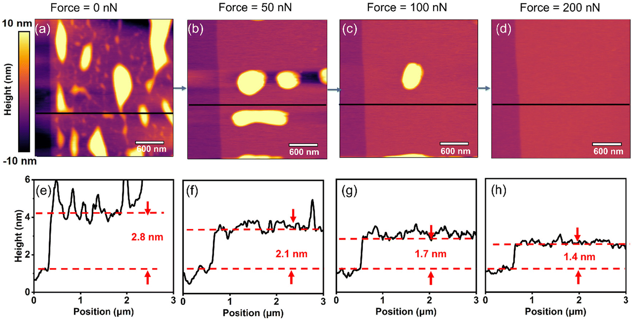 | ||
| Fig. 2 AFM topography images (a–d) and AFM topography line scans (e–h) for nano-spherical probe cleaning of MoS2/hBN with applied force ranging from 0 to 200 nN. As the applied force increases, interlayer bubbles gradually decrease and disappear at 200 nN. The topography line scans correspond to the black lines in (a–e) and show a change in height from 2.8 nm before cleaning to 1.4 nm after cleaning. Consistent with the thickness of bilayer MoS2 in the literature.43,44 | ||
Initial scanning images (Fig. 2a and e) show a bilayer MoS2 with a loosely adhered structure, approximately 2.8 nm height, due to hydrocarbon bubbles and impurities from PDMS dry transfer. Applying a 50 nN load (Fig. 2b) to the bilayer MoS2 reduces its height to 2.1 nm and improves the MoS2/hBN interface adherence. Increasing the force to 100 nN (Fig. 2c) further reduced interlayer bubbles and impurities in the bilayer, although some residual bubbles existed. Ultimately, a 200 nN load (Fig. 2d) achieved complete flattening, diminishing the bilayer height to 1.4 nm. The topographical line scans depicted in Fig. 2a–d are represented in Fig. 2e–h, illustrating significant changes in height. The step height of 1.4 nm in Fig. 2h suggests the successful cleaning of bubbles and contaminants between the MoS2 and the hBN substrate, consistent with the reported thickness for bilayer MoS2.43,44
2.2. Comparison of surface cleaning on MoS2/hBN substrate using nano-spherical and pyramidal probes
Our results highlight the nano-spherical probe is superior to the pyramidal probe in topography and PL. A comparative experiment was done using the nano-spherical and pyramidal probes on the bilayer MoS2/hBN substrate. We focused on two specific areas of a bilayer MoS2/hBN substrate, characterized by the presence of variously sized bubbles. These bubbles were categorized according to their diameters: areas with big bubbles defined as those exceeding 600 nm in diameter, medium bubbles defined from 300 to 599 nm, and small bubbles ranging from 100 to 299 nm. The Hmax/R values (the line is the average value) were obtained from Fig. S7,† consistent with MoS2/hBN substrate in the literature.45,46 The effectiveness of nano-spherical and pyramidal AFM probes in contact mode was evaluated by applying a consistent 100 nN force multiple times. This methodology was used to determine the probes’ effectiveness in cleaning the surface by reducing the presence of bubbles and contaminants.The distribution and quantity of bubbles before and after cleaning with the nano-spherical probe are observable in Fig. 3e, with corresponding AFM scans displayed in Fig. 3a–d. Similarly, bubble distribution and quantity following pyramidal probe cleaning are shown in Fig. 3j, with AFM scans in Fig. 3f–i. The results indicate that the nano-spherical probe effectively cleaned big, medium, and small bubbles during three cleanings, leaving behind only a negligible residual small bubble approximately 100 nm in diameter. In contrast, while the pyramidal probe was efficient in cleaning small bubbles, it was markedly less effective at cleaning big and medium bubbles.
 | ||
| Fig. 3 (a–d) Changes in AFM topography after multiple cleanings at 100 nN using the nano-spherical probe. (e) Changes in the proportions of big, medium, and small bubbles across cleaning scans with the nano-spherical probe. (f–i) Changes in AFM topography after multiple cleanings at 100 nN using the pyramidal probe. (j) Changes in the proportions of big, medium, and small bubbles across cleaning scans with the pyramidal probe. | ||
To further investigate this phenomenon, we selected four distinct regions on the MoS2/hBN material: regions with big bubbles, medium bubbles, small bubbles, and edge regions, for cleaning using both nano-spherical and pyramidal probes. AFM images before and after cleaning are available in ESI (Fig. S3 and S4),† respectively.
The results reveal that the nano-spherical probe effectively cleaned all regions. In contrast, the pyramidal probe is only effective in the small bubble region, partially effective and damaging in the medium bubble region, and completely ineffective and damaging in the big bubble region, causing material damage and warping at the edge region. Fig. S5† presents the scanning electron microscope (SEM) images of the MoS2 regions cleaned with the nano-spherical and the pyramidal probes. The SEM images show that big bubble and edge regions cleaned with the nano-spherical probe are completely cleared, leaving a smooth and uniform surface. In contrast, regions cleaned with the pyramidal probe exhibit material damage, breakage, and incomplete surfaces. This further confirms that the nano-spherical probe excels in non-damaging cleaning of big bubble and edge regions, whereas the pyramidal probe causes material damage during scanning, affecting the intrinsic properties of the material.
The full-width at half-maximum (FWHM) of photoluminescence (PL) is an important factor of material quality, reflecting the radiative lifetime and interactions between excitons and phonons. Higher defect densities in materials impact exciton motion and recombination, broadening the PL linewidth. Additionally, surface roughness and impurities on the substrate lead to uneven distribution of exciton energy levels, further widening the PL linewidth.47–49 To accurately characterize these effects, we compared the PL FWHM before and after cleaning in regions cleaned by the nano-spherical probe, uncleaned regions, and regions cleaned by the pyramidal probe. This comparison demonstrates how different cleaning affect the optical properties of the MoS2/hBN substrate.
To ensure comparability, we selected nano-spherical probe-cleaned, uncleaned, and pyramidal probe-cleaned regions on the MoS2/hBN substrate. Both nano-spherical and pyramidal probes were applied with the same contact force of 200 nN, followed by PL testing.
As shown in Fig. 4a, the region cleaned by the nano-spherical probe (outlined in white) reveals a remarkably smooth surface, free of interlayer bubbles and contaminants, indicating effective impurity removal. Fig. 4c presents the single PL data for the nano-spherical probe-cleaned and uncleaned regions, where the nano-spherical probe region's FWHM is reduced by 30%. The mapping PL FWHM about a 30 μm2 area of both the nano-spherical probe-cleaned and uncleaned regions (Fig. 4b) demonstrates that the cleaned region has a consistent PL FWHM (Fig. 4b, left), averaging 0.085 eV with high uniformity. Fig. 4d provides the detailed FWHM distribution, showing that the probe-cleaned region is concentrated around 0.085 eV, while the uncleaned region is concentrated around 0.115 eV and 0.12 eV.
 | ||
| Fig. 4 (a) AFM topography of the nano-spherical probe-cleaned and uncleaned regions on the MoS2/hBN substrate. (b) PL FWHM mapping of the nano-spherical probe-cleaned region and the uncleaned region in (a). (c) Individual PL spectra of the nano-spherical probe-cleaned and uncleaned regions from (a). (d) The statistical distribution graph of PL FWHM from (b). This shows that the nano-spherical probe can reduce the PL FWHM of the MoS2/hBN substrate, effectively decreasing material contamination. (e) AFM topography of pyramidal probe-cleaned and uncleaned regions on the MoS2/hBN substrate. (f) PL FWHM mapping of the pyramidal probe-cleaned region and the uncleaned region in (e). (g) Individual PL spectra of the pyramidal probe-cleaned and uncleaned regions from (e). (h) The statistical distribution graph of PL FWHM from (f). Although the pyramidal probe also reduces the PL FWHM of the MoS2/hBN substrate, its cleaning performance is inferior to that of the nano-spherical probe due to residual bubbles. | ||
The PL data for the pyramidal probe-cleaned and uncleaned regions are shown in Fig. 4e. Despite the consistent 200 nN contact force, the pyramidal probe-cleaned region still has residual big bubbles, consistent with earlier observations that the pyramidal probe cannot effectively handle big-size bubbles. The pyramidal probe's PL FWHM mapping (Fig. 4f, left) also reveals the impact of residual bubbles on FWHM, without contamination concentrating FWHM around 0.09 eV while residual bubbles cause the FWHM around 0.12 eV. Fig. 4g shows the single PL data for the uncleaned and pyramidal probe-cleaned regions, where the probe-cleaned region's FWHM is reduced by approximately 22% compared to the uncleaned region. The detailed FWHM distribution is shown in Fig. 4h, with the pyramidal probe-cleaned region concentrated centered around 0.09 eV, while residual bubbles also result in values near 0.12 eV. The uncleaned region primarily centers around 0.115 eV and 0.12 eV.
The PL in two-dimensional materials is highly sensitive to strain, doping, and disorder. The peak width is associated with internal disorder, while the peak position is sensitive to doping and strain.43,48,50 Firstly, the PL peak width of the cleaned region is significantly smaller, indicating that the nano-spherical probe reduces the disorder within the MoS2/hBN substrate. Secondly, the number of PL peaks between the nano-spherical probe-cleaned and uncleaned regions remains consistent, showing that the cleaning process does not introduce additional doping.
Thirdly, the PL peak positions in regions cleaned by nano-spherical and pyramidal probes show a blue shift compared to uncleaned regions. This shift occurs because removing bubbles and impurities between MoS2/hBN layers affects the material strain, leading to blue shifting. This observation is consistent with previous literature that suggests bubbles cause the flattening of MoS2 and WS2 materials, resulting in a red shift in PL,51 there is also a slight red shift consistent with the Raman peak reported in the literature,52 it is shown in Fig. S8.† This approach provides a viable solution for future cleaning strategies aimed at preserving the intrinsic properties of materials without causing damage. It also offers the potential to change the position of PL peaks by controlling the strain induced by bubbles.53
To clean the residual bubbles left by the pyramidal probe during the first cleaning (Fig. 4e), a greater force of 300 nN was applied using the pyramidal probe. The area scanned in contact mode after this second cleaning is shown in Fig. 5d. And the exfoliated MoS2/hBN substrate without any cleaning is shown in Fig. 5a. We then tested PL FWHM mapping at 264 points for the nano-spherical probe-cleaned, uncleaned, and pyramidal probe-cleaned regions, as illustrated in Fig. 5e. The statistical distribution of the PL FWHM is displayed in Fig. 5c. Then, we apply Kernel Density Estimation (KDE)54 to the collected PL FWHM to study the data distribution characteristics of these three regions, as shown in Fig. S8b.† KDE is a non-parametric way to estimate the probability density function of a random variable, which helps us visualize how the FWHM values are distributed across the different regions. This approach provides a more detailed insight compared to using traditional histograms, as it smooths the data and reveals the underlying distribution more clearly. Consequently, we obtain the standard deviation in the uncleaned region, as well as in the clean regions of the pyramidal probe and the nano-spherical probe, which are 0.02773, 0.01895, and 0.00531, respectively. The lower standard deviation in the nano-spherical probe-cleaned region indicates a more uniform and consistent PL FWHM distribution, reflecting the probe's effectiveness in minimizing contaminants and improving surface uniformity. In contrast, the higher standard deviation in the uncleaned and pyramidal probe-cleaned regions suggests a less effective cleaning process, leading to greater variability in the PL response, likely due to residual bubbles or surface defects.
 | ||
| Fig. 5 (a) AFM topography of mechanically exfoliated MoS2/hBN substrate without any cleaning. (d) The nano-spherical probe-cleaned region, uncleaned region, and the area cleaned a second time with the pyramidal probe are aimed at cleaning the residual bubbles left after the first cleaning shown in Fig. 4(e). (b) Individual PL spectra of the nano-spherical probe-cleaned, uncleaned, and pyramidal probe-cleaned regions in (d). (e) PL FWHM mapping of the nano-spherical probe-cleaned region, the uncleaned region, and the pyramidal probe-cleaned regions in (d). (c) The statistical distribution graph of PL FWHM from (e). | ||
Fig. 5b illustrates the PL peaks for these three regions. The results reveal that the FWHM of the nano-spherical probe-cleaned region is 70% lower than that of the untreated region. After the second cleaning, the pyramidal probe could not get normal MoS2 PL peaks in some areas, as shown in Fig. 5e right. The increased force scratched the MoS2 surface, potentially damaging its crystal structure and affecting the electronic band structure, leading to a loss of PL. ESI Fig. S6† includes KPFM and SEM images that confirm this observation. The high-resolution SEM imaging of surface potential and morphology revealed scratches and damage, showing that increasing the applied force of the pyramidal probe damaged the MoS2 crystal structure in the process of cleaning bubbles. However, the nano-spherical probe could clean bubbles without increasing the force, avoiding surface damage and reducing the PL FWHM. ESI Fig. S6b (left)† shows that the nano-spherical probe-cleaned region contains fewer contaminants than the untreated region.
2.3. Nano-spherical probe cleaning of interlayer bubbles on MoS2/MoSe2/hBN and WS2/MoS2/hBN sample
After confirming the effectiveness of the nano-spherical probe cleaning for enhancing morphology and photoluminescence of individual type of bilayer TMDs on hBN substrates, we extended our study to cleaning between different TMD layers. We specifically examined MoS2/MoSe2/hBN and WS2/MoS2/hBN samples. Raman spectra verifying the consistency of these samples are shown in ESI Fig. S5.†Fig. 6a–d presents AFM topography images of the MoS2/MoSe2/hBN sample after multiple scans with a 200 nN force applied by a nano-spherical probe, demonstrating a decrease in the number and distribution of big, medium, and small bubbles throughout the scans. | ||
| Fig. 6 (a–d) The AFM topography changes in MoS2/MoSe2/hBN after multiple 200 nN cleanings using the nano-spherical probe. (e) The change of MoS2/MoSe2/hBN in the proportion of big, medium, and small bubbles across cleaning scans. (f–i) The AFM topography changes in WS2/MoS2/hBN after multiple 200 nN cleanings using the nano-spherical probe. (j) The change of WS2/MoS2/hBN in the proportion of big, medium, and small bubbles across cleaning scans. | ||
Similarly, Fig. 6f–i shows AFM scans for the WS2/MoS2/hBN sample under the same conditions, with Fig. 6j summarizing the bubble reduction over three scans.
These results illustrate the nano-spherical probe's effectiveness in cleaning interlayer bubbles, thus improving cleanliness and uniformity across different types of TMD/hBN heterostructures.
3. Discussion
The experimental data provide a comprehensive comparison of the performance between nano-spherical and pyramidal probes in cleaning 2D material interfaces. The nano-spherical probe exhibited superior performance, effectively removing bubbles and contaminants without damaging the material surface, which resulted in a 30% reduction in the PL FWHM of the MoS2/hBN substrate, from 0.115 eV (uncleaned) to 0.08 eV. In contrast, the pyramidal probe struggled with larger bubbles, leaving residues and causing surface damage, as confirmed by KPFM and SEM observations. The pyramidal probe's increased applied force further led to crystal structure damage and inconsistencies in TMD surface morphology.These results highlight the distinct advantages of the nano-spherical probe, which features a smooth surface and uniform contact area.39 The nano-spherical probe, owing to its spherical geometry, as shown in Fig. S1,† establishes a larger contact area with the sample surface. The contact area of nano-spherical probe a(D=500 nm) = 9.24 nm, contact area of the pyramidal probe a(D=10 nm) = 2.51 nm. This results in a more uniform distribution of contact pressure during scanning. The uniform pressure distribution of the spherical probe enhances its ability to effectively compress and displace bubbles and microscopic contaminants without causing damage.
Despite these advantages, the nano-spherical probe also presents several challenges. The production process for the nano-spherical probes is more intricate and costly compared to traditional pyramidal probes.41 Additionally, the AFM probe cleaning method generally has a slower processing speed and lower throughput compared to bulk cleaning methods such as thermal annealing or chemical treatments. This limitation makes it challenging to scale up the use of nano-spherical probes for large-scale applications. To maximize the benefits of nano-spherical probes, further research is needed to explore their integration with other advanced cleaning techniques. This could help enhance overall cleaning efficiency and processing speed, making them more viable for broader applications.
4. Conclusion
The superior performance of the nano-spherical probe over the pyramidal probe in cleaning the interfaces of 2D materials is highlighted. Due to its smooth surface and uniform contact area, the nano-spherical probe avoids scratching or causing physical damage to the material surface during cleaning. Analysis of the PL FWHM indicates that samples cleaned with the nano-spherical probe exhibit lower defect densities and improved material quality. Conversely, pyramidal probes often fail to effectively clean larger bubbles and can damage materials, leading to inconsistent PL characteristics. While AFM probe processing speed and throughput cannot match traditional methods like thermal annealing, AFM probes offer unique benefits in nanoscale real-time observation, in situ processing, and localized cleaning. The nano-spherical probe allows for precise localized cleaning, enabling researchers to clean specific contaminated areas without affecting the structure. This is particularly important for sensitive 2D materials used in research and applications. Additionally, the real-time observation capability of AFM allows operators to monitor the cleaning process visually. Future research should focus on optimizing the fabricating process of the nano-spherical probes to reduce costs and improve scalability. Furthermore, exploring the integration of nano-spherical probes with other advanced cleaning techniques could enhance their overall efficiency and applicability.5. Experiment section
5.1. Mechanical transfer
TMD/hBN samples were fabricated using the following methods:First, a MoS2 crystal was placed on Nitto SPV-224R blue tape and folded back and forth 4–5 times to obtain large MoS2 flakes. Similarly, hBN flakes were obtained by peeling with the blue tape 4–5 times. The hBN flakes were then directly transferred onto a silicon dioxide (SiO2) silicon wafer to create an hBN/SiO2/Si structure. Next, PDMS was cut into small pieces and placed at the center of a glass slide. The PDMS piece was then used to pick up the MoS2 flakes from the blue tape, resulting in thinner MoS2 flakes. Under a microscope, bilayer MoS2 was identified and set aside for transfer. Using a transfer platform, the identified bilayer MoS2 was transferred onto the target hBN/SiO2/Si structure to form the MoS2/hBN/SiO2/Si heterostructure.
5.2. Preparation of nano-spherical probes
Commercially available pyramidal probes were first positioned at a 90-degree angle on an FIB (Focused Ion Beam) stage. Gallium ions were used to etch a 1 μm platform. Then, the probe was placed at a 0-degree angle on the stage, and helium ions were injected to cause the silicon surface to form a small spherical protrusion with a diameter of approximately 600–800 nm.5.3. AFM cleaning and testing
All AFM cleaning and testing experiments were conducted using the MFP-3D from Oxford Instruments. The AFM probes used in the experiments were model AC240TSA-R3.2. After identifying the regions rich in contaminants, we used an AFM in contact mode to remove the polymer contaminants. We selected appropriate areas and applied a contact force of 100 nN to 200 nN. This force range was chosen to effectively remove contaminants while avoiding any damage to the underlying material. The scanning frequency was set to 1 Hz, and the scanning speed was 20 μm s−1, allowing sufficient contact time between the probe and the contaminants for effective removal. The scanning angle was set to 0 degrees, with the probe scanning from top to bottom across the chosen region. If contaminants were not completely removed during the initial pass, multiple scans were conducted to ensure thorough cleaning, more details can be seen in this conference paper.55
3. After the cleaning process, we used AC mode again to re-scan the cleaned area and verify the effectiveness of the cleaning. This step ensured that the polymer contaminants were successfully removed and that the material surface was left in good condition.
5.4. PL and Raman measurements
PL and Raman measurements were conducted using a RENISHAW inVia confocal Raman microscope. A 532 nm laser with either a 50× or 100× objective lens was used for the measurements. The spot size was between 2 to 5 μm. All measurements were performed under laboratory conditions at room temperature.Data availability
All data supporting the findings of this study, including raw experimental results and processed datasets, are provided in the ESI† of the manuscript. These data are fully available for review and reproducibility purposes.Conflicts of interest
There are no conflicts to declare.Acknowledgements
Sincere gratitude is extended to Prof. Huan Hu and Prof. Yang Xu for their invaluable guidance and insightful discussions throughout this research. Appreciation is also given to Paul C. Uzoma and Muhammad Abid Anwar for their language polishing and valuable suggestions. Additionally, thanks to Baoshi Qiao for assistance with essential training on the photoluminescence instrument and Yuxuan Chen for his contribution to mask drawing. Special thanks to Prof. Wee-Liat Ong for providing access to the Raman spectroscopy instrument. Acknowledgment is given to the Micro/Nano Fabrication Center, International Campus, Zhejiang University, with gratitude to the staff for their technical assistance.References
- K. S. Novoselov, et al., Electric field effect in atomically thin carbon films, Science, 2004, 306(5696), 666–669 CrossRef CAS PubMed.
- A. K. Geim and I. V. Grigorieva, van der Waals heterostructures, Nature, 2013, 499(7459), 419–425 CrossRef CAS.
- W. Dong, et al., Toward clean 2d materials and devices: Recent progress in transfer and cleaning methods, Adv. Mater., 2024, 36(22), 2303014 CrossRef CAS.
- A. Thakur and B. Anasori, Accelerating 2D materials discovery, Science, 2024, 383(6688), 1182–1183 CrossRef CAS PubMed.
- R. Li, et al., Layer-coupled corner states in two-dimensional topological multiferroics, Mater. Horiz., 2024, 11(9), 2242–2247 RSC.
- Z. Huang, et al., 2D multifunctional devices: from material preparation to device fabrication and neuromorphic applications, Int. J. Extreme Manuf., 2024, 6(3), 032003 CrossRef.
- Y. Ma, et al., Low-dimensional van der Waals materials for linear-polarization-sensitive photodetection: materials, polarizing strategies and applications, Mater. Futures, 2024, 3(1), 012301 CrossRef CAS.
- A. Ahmed, et al., Recent advances in 2D transition metal dichalcogenide-based photodetectors: a review, Nanoscale, 2024, 16, 2097–2120 RSC.
- A. K. Geim and K. S. Novoselov, The rise of graphene, Nat. Mater., 2007, 6(3), 183–191 CrossRef CAS.
- Y. Yang, et al., From materials to devices: Graphene toward practical applications, Small Methods, 2022, 6(10), 2200671 CrossRef CAS.
- M. Chhowalla, et al., The chemistry of two-dimensional layered transition metal dichalcogenide nanosheets, Nat. Chem., 2013, 5(4), 263–275 CrossRef.
- H. Li, et al., Preparation and applications of mechanically exfoliated single-layer and multilayer MoS2 and WSe2 nanosheets, Acc. Chem. Res., 2014, 47(4), 1067–1075 CrossRef CAS.
- Z. Song, Z. Wang and R. Yu, Strategies for Advanced Supercapacitors Based on 2D Transition Metal Dichalcogenides: From Material Design to Device Setup, Small Methods, 2024, 8(1), 2300808 CrossRef CAS.
- G. Cassabois, P. Valvin and B. Gil, Hexagonal boron nitride is an indirect bandgap semiconductor, Nat. Photonics, 2016, 10(4), 262–266 CrossRef CAS.
- Y. Kubota, et al., Deep ultraviolet light-emitting hexagonal boron nitride synthesized at atmospheric pressure, Science, 2007, 317(5840), 932–934 CrossRef CAS PubMed.
- C. Liu, et al., Two-dimensional materials for next-generation computing technologies, Nat. Nanotechnol., 2020, 15(7), 545–557 CrossRef CAS.
- D. Akinwande, et al., Graphene and two-dimensional materials for silicon technology, Nature, 2019, 573(7775), 507–518 CrossRef CAS PubMed.
- Y. Liu, et al., Van der Waals heterostructures and devices, Nat. Rev. Mater., 2016, 1(9), 1–17 Search PubMed.
- J. Wu, et al., Graphene oxide for photonics, electronics and optoelectronics, Nat. Rev. Chem., 2023, 7(3), 162–183 CrossRef PubMed.
- K. Jiang, et al., Mechanical cleavage of non-van der Waals structures towards two-dimensional crystals, Nat. Synth., 2023, 2(1), 58–66 CrossRef CAS.
- S. J. Haigh, et al., Cross-sectional imaging of individual layers and buried interfaces of graphene-based heterostructures and superlattices, Nat. Mater., 2012, 11(9), 764–767 CrossRef CAS.
- D. Rhodes, et al., Disorder in van der Waals heterostructures of 2D materials, Nat. Mater., 2019, 18(6), 541–549 CrossRef CAS.
- F. K. Perkins, et al., Chemical vapor sensing with monolayer MoS2, Nano Lett., 2013, 13(2), 668–673 CrossRef CAS PubMed.
- Y.-C. Lin, et al., Graphene annealing: how clean can it be?, Nano Lett., 2012, 12(1), 414–419 CrossRef CAS PubMed.
- Z. Cheng, et al., Toward intrinsic graphene surfaces: a systematic study on thermal annealing and wet-chemical treatment of SiO2-supported graphene devices, Nano Lett., 2011, 11(2), 767–771 CrossRef CAS.
- P.-C. Chen, et al., Effective N-methyl-2-pyrrolidone wet cleaning for fabricating high-performance monolayer MoS 2 transistors, Nano Res., 2019, 12, 303–308 CrossRef CAS.
- H. Sunwoo and W. Choi, Tunable, stable, and reversible n-type doping of MoS2 via thermal treatment in N-methyl-2-pyrrolidone, Nanotechnology, 2022, 33(50), 50LT01 CrossRef CAS.
- Y.-D. Lim, et al., Si-compatible cleaning process for graphene using low-density inductively coupled plasma, ACS Nano, 2012, 6(5), 4410–4417 CrossRef CAS.
- P. V. Pham, Cleaning of graphene surfaces by low-pressure air plasma, R. Soc. Open Sci., 2018, 5(5), 172395 CrossRef PubMed.
- M. R. Rosenberger, et al., Nano-“squeegee” for the creation of clean 2D material interfaces, ACS Appl. Mater. Interfaces, 2018, 10(12), 10379–10387 CrossRef CAS.
- Y. Song, et al., Graphene transfer: Paving the road for applications of chemical vapor deposition graphene, Small, 2021, 17(48), 2007600 CrossRef CAS.
- L. P. Ma, W. Ren and H. M. Cheng, Transfer methods of graphene from metal substrates: A review, Small Methods, 2019, 3(7), 1900049 CrossRef.
- Q. Li, et al., Recent advances in oxidation and degradation mechanisms of ultrathin 2D materials under ambient conditions and their passivation strategies, J. Mater. Chem. A, 2019, 7(9), 4291–4312 RSC.
- D. Marinov, et al., Reactive plasma cleaning and restoration of transition metal dichalcogenide monolayers, npj 2D Mater. Appl., 2021, 5(1), 17 CrossRef CAS.
- S. K. Palai, et al., Approaching the Intrinsic Properties of Moiré Structures Using Atomic Force Microscopy Ironing, Nano Lett., 2023, 23(11), 4749–4755 CrossRef CAS PubMed.
- S. Chen, et al., Tip-based cleaning and smoothing improves performance in monolayer MoS2 devices, ACS Omega, 2021, 6(5), 4013–4021 CrossRef CAS.
- C.-M. Liu, et al., Photoluminescence patterns via single-layer exfoliation in Gr/MoS2 heterostructure using contact-mode atomic force microscopy, Appl. Surf. Sci., 2024, 644, 158778 CrossRef CAS.
- Y. Kim, et al., Reliable postprocessing improvement of van der Waals heterostructures, ACS Nano, 2019, 13(12), 14182–14190 CrossRef CAS PubMed.
- P. C. Uzoma, et al., A wear-resistant silicon nano-spherical AFM probe for robust nanotribological studies, Phys. Chem. Chem. Phys., 2022, 24(38), 23849–23857 RSC.
- J. Swadener, E. George and G. Pharr, The correlation of the indentation size effect measured with indenters of various shapes, J. Mech. Phys. Solids, 2002, 50(4), 681–694 CrossRef.
- H. Hu, et al., A sub-micron spherical atomic force microscopic tip for surface measurements, Langmuir, 2020, 36(27), 7861–7867 CrossRef CAS PubMed.
- H. Hertz, The contact of elastic solids, J. Reine Angew. Math., 1881, 92, 156–171 Search PubMed.
- H. J. Conley, et al., Bandgap engineering of strained monolayer and bilayer MoS2, Nano Lett., 2013, 13(8), 3626–3630 CrossRef CAS.
- C. Lee, et al., Anomalous lattice vibrations of single-and few-layer MoS2, ACS Nano, 2010, 4(5), 2695–2700 CrossRef CAS PubMed.
- E. Khestanova, et al., Universal shape and pressure inside bubbles appearing in van der Waals heterostructures, Nat. Commun., 2016, 7(1), 12587 CrossRef CAS.
- M. Gastaldo, et al., Tunable strain and bandgap in subcritical-sized MoS2 nanobubbles, npj 2D Mater. Appl., 2023, 7(1), 71 CrossRef CAS.
- P. Dey, et al., Optical coherence in atomic-monolayer transition-metal dichalcogenides limited by electron-phonon interactions, Phys. Rev. Lett., 2016, 116(12), 127402 CrossRef CAS PubMed.
- M. Selig, et al., Excitonic linewidth and coherence lifetime in monolayer transition metal dichalcogenides, Nat. Commun., 2016, 7(1), 13279 CrossRef CAS PubMed.
- G. Moody, et al., Intrinsic homogeneous linewidth and broadening mechanisms of excitons in monolayer transition metal dichalcogenides, Nat. Commun., 2015, 6(1), 8315 CrossRef CAS PubMed.
- S. Mouri, Y. Miyauchi and K. Matsuda, Tunable photoluminescence of monolayer MoS2 via chemical doping, Nano Lett., 2013, 13(12), 5944–5948 CrossRef CAS.
- A. V. Tyurnina, et al., Strained bubbles in van der Waals heterostructures as local emitters of photoluminescence with adjustable wavelength, ACS Photonics, 2019, 6(2), 516–524 CrossRef CAS.
- K.-Y. Lee, et al., Raman imaging of strained bubbles and their effects on charge doping in monolayer WS2 encapsulated with hexagonal boron nitride, Appl. Surf. Sci., 2022, 604, 154489 CrossRef CAS.
- E. Blundo, et al., Strain-tuning of the electronic, optical, and vibrational properties of two-dimensional crystals, Appl. Phys. Rev., 2021, 8(2), 021318 CAS.
- Y.-C. Chen, A tutorial on kernel density estimation and recent advances, Biostat. Epidemiol., 2017, 1(1), 161–187 CrossRef.
- X. Ding , et al., Damage-Free Cleaning of 2D van der Waals Heterostructures with Nano-Spherical AFM Probes, in 2023 IEEE 23rd International Conference on Nanotechnology (NANO), IEEE, 2023.
Footnote |
| † Electronic supplementary information (ESI) available. See DOI: https://doi.org/10.1039/d4nr03583f |
| This journal is © The Royal Society of Chemistry 2025 |