
Stacking dependent piezoelectric response of bilayer and heterobilayer group-IV monochalcogenides under applied external strain†
Kevin
Tran
 and
Michelle J. S.
Spencer
*
and
Michelle J. S.
Spencer
*
School of Science, RMIT University, GPO Box 2476, Melbourne, Victoria 3001, Australia. E-mail: michelle.spencer@rmit.edu.au
First published on 3rd February 2025
Abstract
Layered two-dimensional (2D) materials are promising materials for piezoelectric and optoelectronic devices due to the introduction of new and interesting properties not seen in the single layers alone. In particular, the group-IV monochalcogenides (MX, M = Ge/Sn and X = S/Se) are highly piezoelectric layered materials which have outstanding optical adsorption properties in the isolated monolayer form. It is possible that combinations of MX monolayers, in a bilayer or heterobilayer system, could exhibit properties that are different to their monolayer counterparts. Using density functional theory calculations, the stacking-dependent piezoelectric response of group-IV monochalcogenide bilayers and heterobilayers with and without applied strain was determined. Of the four materials, SnSe yields the largest e22 value in both the monolayer (0.86 C m−2) and bilayer (1.36 C m−2) form. Of the different heterobilayers examined, GeSe/SnSe has the largest e22 value (1.58 C m−2). With the application of strain, the piezoelectric response can be significantly enhanced, allowing bilayer SnSe to achieve a maximum response of 6.13 C m−2, which is a ∼450% increase compared to its unstrained form, and is 450–730% higher than reported for other layered materials, such as ZnO and MoSTe. Indirect-to-direct band gap transitions can also be achieved using differing stacking arrangements, with the GeSe/SnSe heterobilayer being determined to have a type II band gap, demonstrating there are potential applications for the heterobilayers in optoelectronic devices. Overall, the group-IV monochalcogenide bilayers have the potential to achieve extraordinary piezoelectric responses under applied strain, making them ideal for nano-based piezoelectric and optoelectronic devices.
1. Introduction
Two-dimensional (2D) materials, particularly 2D monolayers, have attracted significant interest in materials science due to the outstanding properties that their bulk counterparts do not have. For example, graphene functionalized with O, Li and F atoms can exhibit piezoelectric responses higher than graphite, while other materials, such as MoS2, can change from being an indirect band gap semiconductor in its bulk form to a direct band gap semiconductor when reduced to a monolayer.1–4The group-IV monochalcogenides, GeS, GeSe, SnS and SnSe (MX, M = Ge or Sn, X = S or Se) have extraordinary structural and electronic properties. They have been synthesized using facile solution-based approaches,5 physical vapor deposition6 and molecular beam epitaxy.7 With a puckered layered orthorhombic structure that is similar to black phosphorus, MX monolayers can achieve tensile strains up to 45% along the armchair direction, making them ideal flexible materials.8 This flexibility, in addition to their non-centrosymmetric structure, allows MX monolayers to exhibit piezoelectric properties that are larger than other well-known piezoelectric materials, such as ZnO9 and MoS2.10 With the introduction of strain, monolayer SnSe can achieve significant enhancements to its piezoelectricity, increasing its response by 3.33 times using a compressive strain of 3.5%.11 However, it is not known whether the other MX monolayers can achieve the same enhancement in their piezoelectric response.
Combining monolayers into heterostructures can also further enhance their properties.12 For example, MX monolayers have indirect band gaps similar to their bulk form making them difficult to be used in some applications, such as solar cells.13–15 In the bilayer form, all four materials undergo indirect to direct band gap transitions as a result of the interlayer interactions of the different stacking arrangements.16 The alignment of the two stacked layers relative to each other can also affect their polarisation properties. When stacked directly on top of one another, bilayer SnSe has ferroelectric (FE) polarisation, however, sliding one layer with respect to the other along the armchair direction induces a reversible ferroelectric-to-antiferroelectric (AFE) transition.17 Similarly, the GeSe/SnS heterobilayer loses it polarisation when arranged in an AFE state, however, while in its FE state it has a dipole moment.18 This suggests that by combining group-IV monochalcogenide monolayers in various stacking patterns, polarisation can be induced, and may lead to higher piezoelectric responses than can be achieved in the monolayers alone. Furthermore, the formation of heterobilayers often results in some degree of lattice mismatch between the two layers, which can induce changes to the electronic and other properties of the material. For example, the lattice mismatch between ZnO and CeO2 layers can improve the overall piezoelectric performance.19
The piezoelectric and optoelectronic properties of all the MX bilayers and heterobilayers, however, is not known. It is also not known how applied strain may affect their piezoelectric responses.
In this work, density functional theory (DFT) calculations were performed to determine the electronic and piezoelectric properties of MX bilayers and heterobilayers, with and without applied strain. The results provide insights into how the properties of bilayer MX heterostructures can be modified for piezoelectric and optical device applications.
2. Computational details
The calculations in this work were performed using DFT as implemented in the Vienna ab initio Simulation Package (VASP).20,21 The exchange correlation functional in the Perdew–Burke–Ernzerhof (PBE) form was adopted and the ion-electron interaction was described by the projector augmented wave (PAW) method.22,23 The plane-wave energy cut-off was set to 600 eV. All atoms in the system were allowed to relax until the total energy was converged to 1 × 10⁻⁶ eV and the Hellman-Feynman force on each relaxed atom was less than 0.01 eV Å−1. The Grimme DFT-D3 approach was applied to account for the van der Waals forces.24 The calculated lattice parameters of monolayer GeS, GeSe, SnS and SnSe were a = 3.66 Å, 3.87 Å, 4.02 Å, 4.21 Å and b = 4.45 Å, 4.38 Å, 4.44 Å, 4.52 Å, respectively, which are within 5% of previous experimental and theoretical values.25 The lattice parameters used for the heterobilayers were determined by calculating the average a- and b- parameters of the two layers, as shown in Table S1.† The monolayers and bilayers were modelled using periodic boundary conditions with a vacuum spacer of 20 Å applied along the c-direction to avoid interlayer interactions.A Γ-centred k-point mesh with dimensions of 9 × 9 × 1 and 9 × 9 × 2 was adopted for the monolayer and bilayer systems, respectively. It is known that the PBE functional underestimates the band gap, therefore, the hybrid Heyd–Scuseria–Ernzerhof (HSE) functional was used to ensure accurate band structures were calculated.26
The piezoelectric properties of the monolayer and bilayer systems were calculated using the density functional perturbation theory (DFPT) method implemented in VASP.27–29 The piezoelectric constants, eijk, were evaluated from the two terms, Pi and εjk which represent the polarization vector and stress tensors, respectively:30
The subscript i = 1, 2 and 3, represents the direction of polarization along the x-, y- and z- directions, respectively.
In Voigt-notation, the εjk term can be written as εj, resulting in the piezoelectric stress constant to be evaluated as:30

With a constant electric field, the eij term can also be related to the piezoelectric strain constant, dij, if the elastic constants, Cjk, are known:
| eik = dijCjk |
For the monolayer group-IV monochalcogenides, which belong to the Pmn21 space group, we have calculated the piezoelectric constants, e11, e22, e21 and the elastic constants, C11, C22 and C12.9
e
22 and e21 can be evaluated as:
| e22 = d22C22 + d12C12 |
| e21 = d22C12 + d12C12 |
In this work, we only consider the relaxed-ion piezoelectric stress constants, eij, which include both the ionic and electronic contributions obtained by the DFPT calculations.
The primary piezoelectric constant calculated is e22 which was previously shown to have the highest response for the group-IV monochalcogenides due to their high flexibility along the armchair direction.9 However, we also calculate the e11 and e21 constants. As the k-point density per reciprocal atom (KPPRA) used for the DFT convergence parameters is not sufficient to calculate accurate piezoelectric constants, a KPPRA of 3000 was used, corresponding to a k-point mesh of 14 × 14 × 2.31
3. Results and discussion
3.1 Group-IV monochalcogenide monolayers
The calculated e22 values for the 4 monolayers are 0.36, 0.54, 0.66 and 0.86 C m−2 for GeS, GeSe, SnS and SnSe respectively, showing the same order (along the armchair direction) reported in previous studies.9,10 The e22 values under biaxial (ε12) and uniaxial (ε22) strains of ±6% are shown in Fig. 1.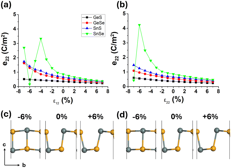 | ||
| Fig. 1 Piezoelectric constant, e22, of monolayer GeS, GeSe, SnS and SnSe under applied (a) biaxial and (b) uniaxial strain along the armchair direction. The structures of monolayer SnSe are shown at the strain values indicated for (c) biaxial and (d) uniaxial strain. The grey and orange spheres represent the Sn and Se atoms, respectively. | ||
For biaxial strain (Fig. 1a), the e22 value for all 4 monolayers decrease for tensile strain values up to 6%. In contrast, for compressive strain, the e22 increases. Monolayer SnSe achieves the highest value, with a maximum e22 of 3.33 C m−2 with 4% strain; at higher compressive strains, the e22 decreases significantly as the monolayer undergoes a phase change from Pnm21 to P4/nmm. The e22 for the other monolayers increases for compressive strains up to 6%, however, the values are much smaller than can be achieved for SnSe. Monolayer GeS, GeSe and SnS do not undergo phase transformations as the M and X atoms along the armchair direction are not aligned along the y-direction, hence, the structure is still non-centrosymmetric, as shown in Fig. S1† This is not the case with monolayer SnSe, which underwent a phase change, with the Sn and Se atoms being aligned above each other along the armchair direction, hence, creating a centrosymmetric structure with weak piezoelectric responses.
Interestingly, after the phase change occurs for monolayer SnSe, the structure becomes buckled again with additional compressive strain. At −7% strain, the relative vertical position of the M and X atoms becomes misaligned creating non-centrosymmetry again, which allows for piezoelectric properties as shown in Fig. S2a.† As the strain is increased to −8%, the M and X atoms become more aligned vertically again, resulting in the subsequent decrease in the e22 value.
For uniaxial strain along the armchair direction (Fig. 1b), there is a similar trend in the e22 values as was calculated for biaxial strain. Again, SnSe achieves the highest piezoelectric response of 4.30 C m−2 with a 5% compressive strain. Beyond 6%, the phase change (from Pnm21 to P4/nmm) results in the e22 decreasing below that of the unstrained system, which is in agreement with previous results.11 Unlike with biaxial compression, for compressive strains greater than 6%, the e22 values remain small as the monolayer does not become buckled and maintains its centrosymmetry as shown in Fig. S2b.†
For uniaxial strain along the zig-zag direction (ε11) (Fig. S3†), the e22 value for all 4 monolayers does not increase significantly with compressive or tensile strain. The highest increase occurs for SnSe, which achieves a piezoelectric response of 1.16 C m−2. Hence, straining the monolayers along the zigzag direction does not result in an enhancement of the piezoelectric response.
For uniaxial strain along the c-direction, the position of the upper layer M and X atoms was increased or decreased at discrete values along the z-axis to represent different degrees of expansion and contraction, respectively. A geometry optimisation calculation was then performed at each strain value, keeping the M atoms fixed while allowing all other atoms to relax in the x-, y- and z-directions. This process ensures the monolayer retains its expansive or contractive strain along the c-direction, while allowing for the system to also relax at each value. The e22 responses were calculated to have enhancements similar in magnitude to those when the material was strained along the zig-zag direction (Fig. S4†). Of the 4 monolayers, SnS achieves the largest increase in e22 (1.03 C m−2 with compressive strain). Therefore, compressing the M–X bonds along the c-direction is not as effective in enhancing the piezoelectric response of the monolayers as the y-direction (armchair), which increases the non-centrosymmetry.
The increase in e22 with compressive (but not tensile) strain, for all 4 monolayers can be attributed to the fact that compressive strain makes the bilayers become more buckled, increasing the non-centrosymmetry, until a phase change occurs that results in the structure becoming centrosymmetric.
For e21, there are small enhancements in the piezoelectric response with biaxial strain, with monolayer SnSe achieving a value of 0.53 C m−2 for a strain value of −4%, before significantly decreasing with larger compressive strain values (Fig. S5†). The sharp drop in the piezoelectric response corresponds with the phase change noted when discussing the e22 values. For uniaxial strain, the enhancement is even greater, with SnSe achieving an e21 of 1.17 C m−2 before undergoing a phase change beyond −6% strain. However, the overall magnitude of the e21 values is smaller than the e22 values, meaning that it would be more efficient to enhance the e22 response when applying strain to the materials.
3.2 Group-IV monochalcogenide bilayers
There are 4 different possible stacking orders that are considered for the MX bilayers, being the AA-, AB-, AC- and AD- stacking arrangements (as shown in Fig. 2). AA-stacking refers to the top layer being aligned directly above the bottom layer, in the exact same alignment. In the AB-stacking arrangement, the top layer is shifted half a lattice constant along the y-direction compared to the AA alignment. Shifting the top layer by half a lattice constant along the x-direction (compared to the AA-alignment) gives the AC-stacking arrangement. Shifting the top layer by half a lattice constant along the y-direction (compared to the AC position) yields the AD-stacking configuration. | ||
| Fig. 2 Top and side views of the different stacking arrangements for the group-IV monochalcogenide bilayers. The grey and yellow atoms represent the M (Ge/Sn) and X (S/Se) atoms, respectively. | ||
Of the four stacking arrangements, the AC-stacking geometry was determined to be the most energetically stable, in agreement with previous studies (Table S2†).17,18 The e22 values for each of the bilayers were the smallest for this arrangement (Fig. 3) and largest for the AD-stacking arrangement (except for bilayer SnS, where e22 was largest in the AB-stacking arrangement). Overall, bilayer SnSe had the largest e22 value (1.36 C m−2), similar to its monolayer counterpart, however, the value is larger than the monolayer by 37%. Therefore, creating bilayers of the group IV monochalcogenides, can create enhanced piezoelectric responses.
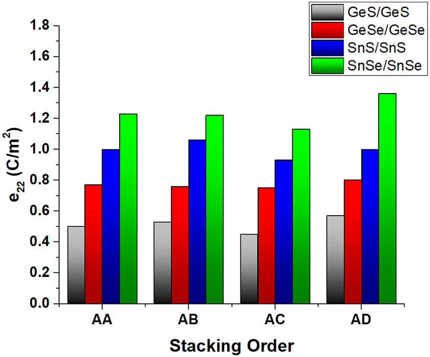 | ||
| Fig. 3 Calculated e22 values of the group-IV monochalcogenide bilayers in the 4 stacking arrangements indicated. | ||
The calculated e22 values for each stacking arrangement can be correlated with the elastic constant (C22) (Fig. 4). In general, a higher e22 value corresponds to a smaller C22 value,32–34 meaning that the structures with a lower C22 have weaker M–X covalent bonds allowing it to be more flexible and hence can allow for a higher piezoelectric response. We also find there is some correlation between e22 (and e21) and C12 (see Fig. S6 and S7†). For example, for GeSe in the AB- and AC- stacking arrangements, the C12 values are higher than for the other bilayers, suggesting stronger M–X covalent bonds, while for SnS in the AB-stacking arrangement, C12 is low which may contribute to weakening of the M–X bonds in that specific stacking configuration. For GeSe and SnSe, in particular, the C12 value tends to increase as e21 decreases.
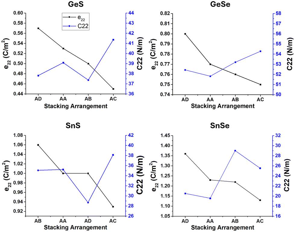 | ||
| Fig. 4 Calculated e22 and C22 values of the group-IV monochalcogenide bilayers in different stacking arrangements. | ||
Given the SnSe bilayer was calculated to have the largest piezoelectric constant, strain was applied to this system to determine if the e22 value could be further enhanced. The relative energies of the bilayer with strain are small, with the largest change being an increase of 0.35 eV (Fig. S8†). Fig. 5 shows the e22 values after applied biaxial (ε12) and uniaxial strain along the armchair direction (ε22) for the 4 stacking arrangements.
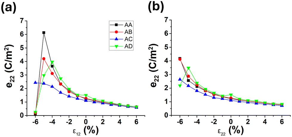 | ||
| Fig. 5 Calculated e22 values of bilayer SnSe in different stacking arrangements under (a) biaxial strain and (b) uniaxial strain along the armchair direction. | ||
For biaxial strain (Fig. 5a), the AA-stacking arrangement achieved a maximum e22 value of 6.13 C m−2 with a compressive strain of 5%, before the bilayer underwent a phase change (see Fig. S9a†) which drastically decreases the e22 value. For both the AB- and AD- stacking arrangements, the maximum e22 value achieved was 4.20 and 3.97 C m−2, respectively, before they underwent a phase change (Fig. S9b and d†). For the AC-stacking geometry the increase in the piezoelectric response is smaller, achieving a value of 2.43 C m−2, however, compared to the other stacking arrangements, there is no phase change (see Fig. S9c†).
For uniaxial strain (Fig. 5b), both the AA- and AB- stacking arrangments achieve maximum e22 values of 4.17 and 4.11 C m−2, respectively, which are similar to the monolayer value (4.30 C m−2). In the AD-stacking geometry, a maximum value of 3.48 C m−2 is achieved with 5% compression before it undergoes a phase change. Again, the AC-stacking geometry has the weakest piezoelectric response with compressive strain, achieving a maximum value of 2.63 C m−2, and again not undergoing any phase change with 6% compressive strain (Fig. S10†).
Overall, application of biaxial strain is more effective in enhancing the piezoelectric response. The largest enhancement that was achieved with any strain value investigated was ∼30% greater than that of the monolayer under the same strain value. When compared to unstrained SnSe, the enhancement is up to 450%, which is significant. Similarily, this is a 450%–730% increase compared to other common piezoelectric materials such as ZnO and MoSTe heterobilayers.35–38
For e21 upon biaxial strain, the piezoelectric response reaches a maximum of 2.83 C m−2 with −4% strain in the AA-stacking arrangement, before undergoing a phase change as shown in Fig. S11.† For uniaxial strain, the maximum e21 achieved is 1.00 and 0.95 C m−2, for the AA- and AB- stacking arrangements, respectively.
3.3 Group-IV monochalcogenide heterobilayers
The calculated e22 values of the heterobilayers, consisting of two different group-IV monochalcogenides, are shown in Fig. 6. Again, there are 4 different stacking arrangements possible and the e22 for each is presented. Similar to the bilayer systems, the AC-stacking geometry is the most energetically stable (see Table S2†), followed by AB- > AA- > AD- stacking geometry. | ||
| Fig. 6 Calculated e22 of group-IV monochalcogenide heterobilayers in different stacking orders. | ||
The heterobilayers that consist of SnSe combined with one of the other 3 monolayers (GeS, GeSe or SnS) were determined to have the largest piezoelectric response in all stacking alignments. The largest e22 value achieved was for GeS/SnSe in the AB-stacking arrangement, which has a standout value of 1.58 C m−2, which is ∼14% larger than the (unstrained) bilayer SnSe system.
For these systems, there is already some degree of strain applied to the system due to the lattice mismatch. We chose to calculate the effect of (further) strain on the GeS/SnSe and GeSe/SnS heterobilayers, as they have the largest (7.8%) and smallest (1%) lattice mismatch values, respectively (see Table S3†).
For both biaxial and uniaxial tensile strain, the e22 of GeS/SnSe decreases in all stacking arrangements (Fig. 7). The specific stacking alignments are also maintained (see Fig. S12†), and no sliding occurs with expansion.
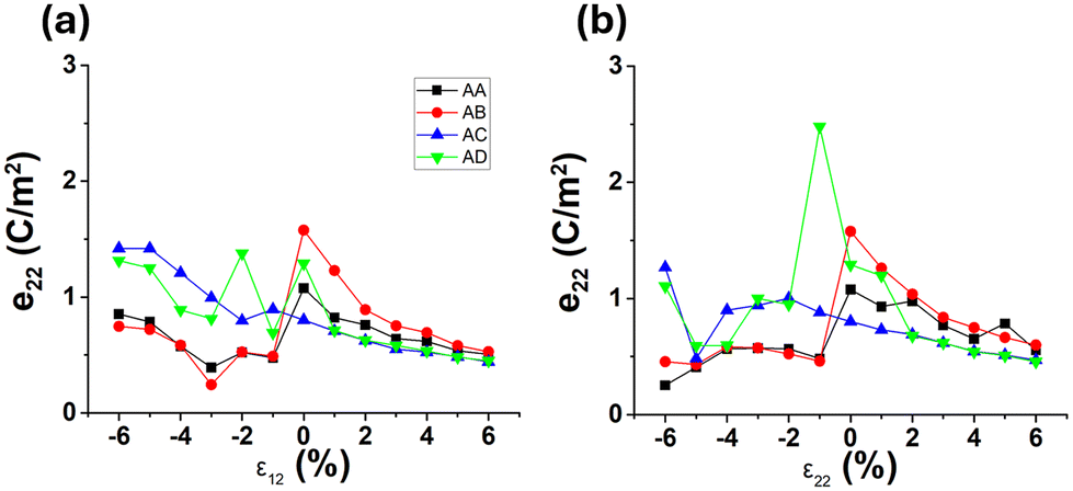 | ||
| Fig. 7 Calculated e22, of the GeS/SnSe heterobilayer in different stacking arrangements under (a) biaxial strain and (b) uniaxial strain along the armchair direction. | ||
For biaxial compressive strain (Fig. 7a), the e22 value decreases for the AA and AB stacking arrangements and increases for the AC and AD stacking alignments. The decrease is due to the SnSe layer realigning into a more stable stacking arrangement, as well as undergoing a phase change, as a result of the strain. For example, the e22 values for AA/AB (red and black lines) are almost identical for a 1% strain, which indicates that the AA-stacking has relaxed into the AB-stacking, as shown in Fig. S12a and b.† For the AD-stacking geometry (green line), the e22 value is almost equal to the AC-stacking geometry (blue line) for a 1% strain, indicating the layers slide past each other, from an AD- to an AC- stacking alignment (see Fig. S12c and d†). As the compressive strain is increased to 2%, the layers move back to an AD-stacked alignment before sliding back into the AC-stacking with higher strain values. With further increases in the compressive strain, the e22 value for the AD-stacking alignment remains similar to that for the AC-stacking alignment. The AC-stacked heterobilayer maintains its configuration with compressive strain, achieving a value of 1.42 C m−2 (at 6%) which is a 44% increase compared to its non-strained value.
For uniaxial compression (Fig. 7b), similar trends are seen for the AA-stacked bilayer, which relaxes into an AB-stacking configuration with compressive strain, leading to equal e22 values. For the AD-stacking alignment, there is a sharp increase in the e22 value with a 1% compressive strain, achieving an e22 of 2.47 C m−2. For larger strains, the bilayers relax into the AC-stacked arrangement, resulting in similar e22 values.
For the GeSe/SnS heterobilayer, all stacking arrangements relax into a more stable alignment under both biaxial and uniaxial tensile strain (Fig. 8). The AA- and AD- stacking arrangements relax into an AB- and AC- stacking alignment (Fig. S13†), respectively, with no enhancement of the e22 value, similar to the monolayer and bilayer systems.
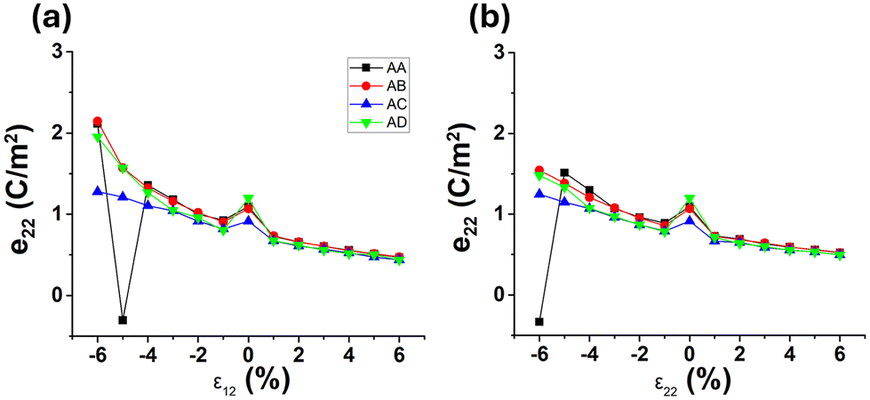 | ||
| Fig. 8 Calculated e22 of the GeSe/SnS heterobilayer in different stacking arrangements under (a) biaxial strain and (b) uniaxial strain along the armchair direction. | ||
For biaxial compression (Fig. 8a), some of the stacking geometries relax to the same alignment with the AA- and AB- stacking alignments achieving maximum e22 values of 2.12 C m−2 and 2.15 C m−2, respectively, with a 6% compressive strain. These values are ∼50% larger than their corresponding non-strained value.
The large decrease in the e22 value in the AA-stacking alignment with a 5% compressive strain is a result of the heterobilayer switching into an anti-ferroelectric (AFE) state. This state occurs when the two layers are antiparallel to each other, as shown in Fig. S15,† where the M–X bonds along the armchair direction in each layer are opposite to each other. Previous studies17,18 have shown that MX bilayers in an AFE state have essentially no polarity, therefore, given that piezoelectricity is dependent on a dipole, it is not expected there is a piezoelectric response, in agreement with our calculations. To validate this, e22 for the GeSe/SnS heterobilayer was calculated along a sliding pathway, from an FE state (AC-stacked) to an AFE state (AB-/AD-stacked). As the top SnS layer slides into an ABAFE-/ADAFE-stacked position, the horizontal Sn–S covalent bonds break, and reconnect with another neighbouring Sn/S atom (Fig. S15†). This results in the piezoelectric response decreasing significantly to a near zero value.
3.4 Electronic properties of the group-IV monochalcogenide monolayers, bilayers and heterobilayers
In this section we investigate the electronic properties of the bilayers as a function of composition and applied strain. In Table 1 are the calculated HSE06 band gaps of the monolayers, bilayers and heterobilayers in the different stacking arrangements investigated.| Band gap (eV) | Alignment | ||||
|---|---|---|---|---|---|
| AA | AB | AC | AD | ||
| a Direct band gap. | |||||
| GeS | 2.41 | — | — | — | — |
| GeSe | 1.70a | — | — | — | — |
| SnS | 2.24 | — | — | — | — |
| SnSe | 1.58 | — | — | — | — |
| GeS/GeS | 2.07a | 1.76 | 2.15a | 1.72 | — |
| GeSe/GeSe | 1.49 | 1.58 | 1.69a | 1.38 | — |
| SnS/SnS | 1.92 | 1.47 | 2.05a | 1.63 | — |
| SnSe/SnSe | 1.28 | 1.34 | 1.48a | 1.11 | — |
| GeS/GeSe | 1.25 | 1.32 | 1.50 | 1.15 | I |
| GeS/SnS | 1.58 | 1.53 | 1.77 | 1.52 | I |
| GeS/SnSe | 0.46 | 0.72 | 0.97 | 0.34 | I |
| GeSe/SnS | 1.51a | 1.70 | 1.68a | 1.49 | II |
| GeSe/SnSe | 0.68 | 1.07a | 1.10a | 1.48 | I/II |
| SnS/SnSe | 1.51 | 1.13 | 1.50 | 0.82 | I |
For all four monolayers, the band gap is indirect (Fig. S16†), with the calculated values being in agreement with previous studies.25 GeSe also has a direct band gap which is only a few meV larger than the indirect gap.
For the bilayer systems, the order of the band gap is generally the same as it is for the monolayers in all 4 stacking alignments, however, the magnitude varies with the stacking arrangement (Table 1 and Fig. S17†).
In the AA-stacking geometry, the band gaps narrow by approximately 0.3 eV compared to the monolayer, while remaining indirect. It should be noted there is a direct gap for bilayer GeS which is 0.01 eV larger than the indirect one.
In the AB-stacking arrangement, the band gap narrows by 0.65 eV, 0.12, 0.77 and 0.24 eV, for the GeS, GeSe, SnS, and SnSe bilayers, respectively, while remaining indirect.
In the AC-stacking arrangement, the band gap narrows, but by smaller amounts of 0.26, 0.01, 0.19 and 0.10 eV for bilayer GeS, GeSe, SnS, and SnSe, respectively. Interestingly, all bilayers undergo an indirect–direct band gap transition. GeSe does maintain an indirect band gap that is only 0.01 eV larger than the direct one.
In the AD-stacking geometry, the band gap narrows by 0.69, 0.32, 0.61 and 0.47 eV for bilayer GeS, GeSe, SnS, and SnSe, respectively, while remaining indirect.
Hence, the creation of bilayers in different stacking alignments can be used as an approach to tune the electronic properties of the monolayers.
For the heterobilayers (Fig. 9 and Table 1), the largest band gap achieved is 1.77 eV for GeS/SnS in the AC-stacking geometry. The band alignment corresponds to a type-I alignment as the VBM and CBM both come from the SnS layer (red line).
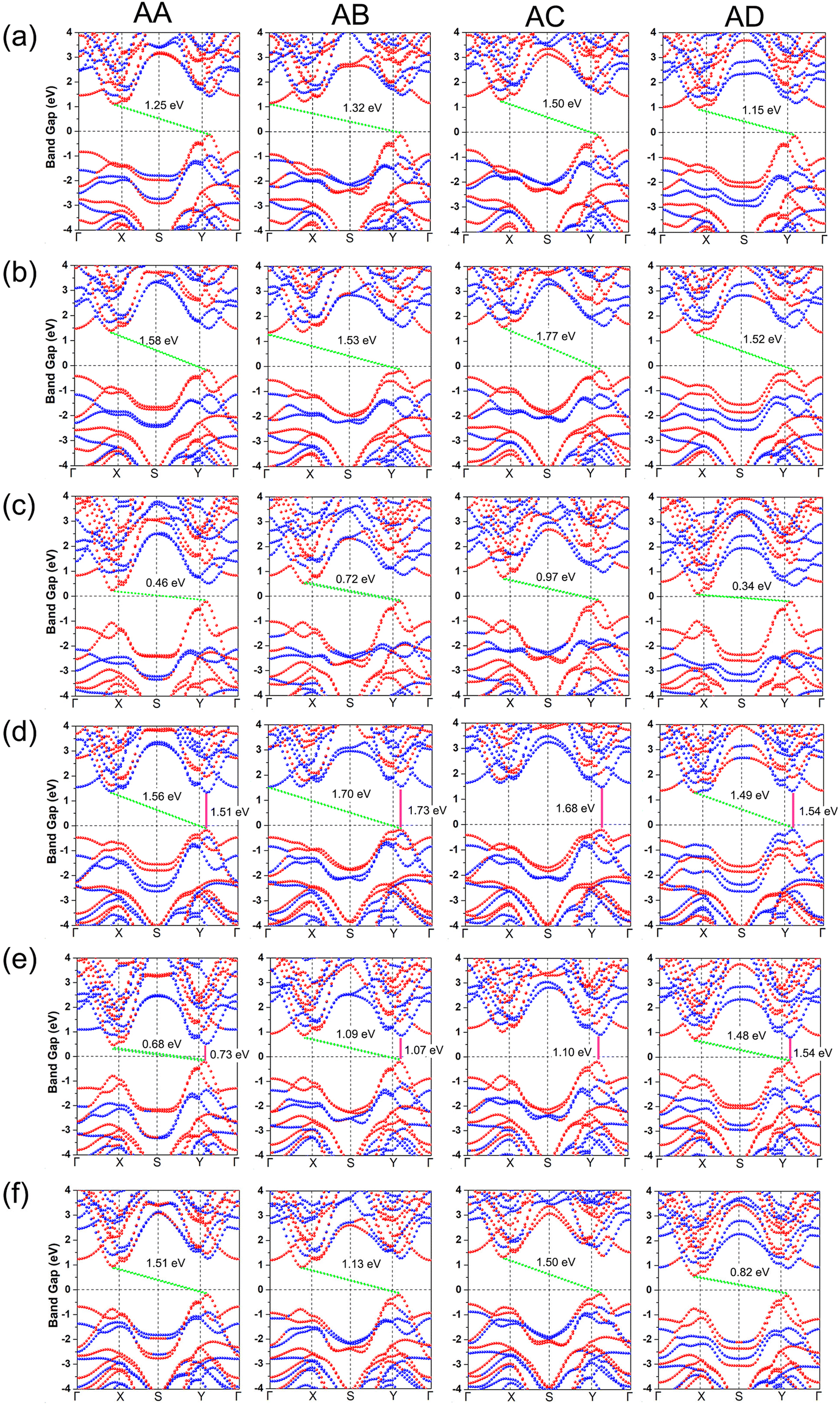 | ||
| Fig. 9 Projected band structures of the (a) GeS/GeSe, (b) GeS/SnS, (c) GeS/SnSe, (d) GeSe/SnS, (e) GeSe/SnSe and (f) SnS/SnSe heterobilayers in the different stacking alignments. The red and blue lines refer to the top and bottom layers, respectively. The green and pink lines represent the indirect and direct band gaps, respectively. | ||
The smallest band gap (0.34 eV) is achieved for GeS/SnSe in an AD-stacking alignment. The large narrowing of the gap could be attributed to the large lattice mismatch of this system, where the SnSe layer was compressed in order to create the heterobilayer. This effect of band gap narrowing with compressive strain has been previously reported for other 2D materials.39,40 Despite the reduction in the band gap, it remains indirect and has a type-I band alignment. Having a type-I band alignment means the system can undergo recombination of electrons and holes when irradiated by light. This makes it advantageous for photocatalyst applications, such as in LED devices.41,42
For the GeSe/SnS (Fig. 9d) bilayer in the AA- and AC- stacking arrangements, there is an indirect-direct transition. However, for these structures, both the indirect and direct band gaps are only a few meV different in magnitude. The system has a type-II band alignment as the GeSe (blue) and SnS (red line) contribute to the VBM and CBM, respectively. This creates a staggered gap and allows for effective separation of electrons and holes, which can be useful for photovoltaic applications, such as solar cells.43
For the GeSe/SnSe bilayer (Fig. 9e), there are also indirect-direct transitions for the AB- and AC- stacking arrangements. For this system, the band alignment is dependent on the band gap being direct or indirect. For AA- and AD- stacking alignments, the band gap is indirect which results in a type I band alignment. For AB- and AC- stacking alignments, the band gap is direct giving a type-II band alignment. Hence, an AB- or AC- stacking alignment is preferable for optoelectronic applications. It is important to note that given both the indirect and direct band gaps are only a few meV different, any form of external stimuli, such as strain or defects, could change the band alignment of the bilayer.
Comparing the band gap values with the piezoelectric responses, it can be seen that the GeS/SnSe heterobilayer, which has the narrowest band gap in all stacking arrangements (Table 1) has the largest piezoelectric response (Fig. 6). In general, heterobilayers with wider band gaps, namely, GeS/GeSe, GeS/SnS and GeSe/SnSe, tend to have weaker piezoelectric responses. In addition, for both the bilayer and heterobilayer structures, the band gap is widest for the most stable AC-stacking alignment. However, when compared to other common piezoelectric materials such as ZnO, which has a wide band gap of ∼3.2 eV,44 the heterobilayers have the advantage of a narrow band gap which allows for the adsorption of visible light, and hence could be used in LED devices. Furthermore, having a highly piezoelectric material that has a narrow band gap allows it to be used in a wide variety of applications such as in piezo-photoelectrochemical water splitting devices and in piezo-phototronics.45,46
Conclusion
In summary, large piezoelectric enhancements are achievable for the bilayer and heterobilayer monochalcogenide (MX) systems using different stacking alignments, as well as applied compressive strain. Of the four MX materials, SnSe yields the highest piezoelectric response in both its monolayer (0.86 C m−2) and bilayer (1.36 C m−2) form. When the MX monolayers are used in a heterobilayer, GeSe/SnS achieves the largest e22 value of 1.58 C m−2 which is ∼14% larger than bilayer SnSe.When compressive strain up to 5% is applied, the piezoelectric response of bilayer SnSe, in an AA-stacking arrangement, is significantly increased, achieving a maximum e22 value of 6.13 C m−2 which is 450% larger than the unstrained system. Such a large increase in the e22 value cannot be achieved for the heterobilayers due to the lattice mismatch, which caused them to either slide into another stacking arrangement or switch into an AFE state.
The different stacking arrangements investigated for the bilayers and heterobilayers can result in indirect-direct band gap transitions and cause a narrowing or widening of the band gap. From the different heterobilayer combinations, GeSe/SnS has a type-II band alignment in the AA- and AD- stacking arrangements, while GeSe/SnSe has a type-II band alignment when arranged in AB- or AC- stacking alignment, making them ideal for optoelectronic device applications that require charge separation.
A narrowing of the band gap can also be correlated with an increase in the e22 values. Specifically, GeSe/SnS which has the smallest band gap of all the systems investigated has the strongest piezoelectric response without any applied strain.
Overall, the results from this work demonstrate that both the piezoelectric response and the optical properties of bilayer 2D materials can be tuned by using different stacking geometries, applied strains and bilayer compositions, making them ideal for nano-based piezoelectric and optoelectronic devices.
Author contributions
The manuscript was written with contributions from all authors. All authors have given approval to the final version of the manuscript.Data availability
All relevant data that supports the findings are included within the manuscript (and any ESI†).Conflicts of interest
There are no conflicts to declare.Acknowledgements
This work was supported by the Australian Government's National Collaborative Research Infrastructure Strategy (NCRIS), with access to computational resources provided by the National Computational Infrastructure (NCI) Facility and Pawsey Supercomputing Research Centre, through the National Computational Merit Allocation Scheme. Kevin Tran acknowledges RMIT University for their RMIT Research Stipend Scholarships award.References
- M. T. Ong and E. J. Reed, Engineered Piezoelectricity in Graphene, ACS Nano, 2012, 6(2), 1387–1394 CrossRef CAS PubMed.
- Z. Chang, W. Yan, J. Shang and J. Z. Liu, Piezoelectric properties of graphene oxide: A first-principles computational study, Appl. Phys. Lett., 2014, 105(2), 023103 Search PubMed.
- K. K. Kam and B. A. Parkinson, Detailed photocurrent spectroscopy of the semiconducting group VIB transition metal dichalcogenides, J. Phys. Chem., 1982, 86(4), 463–467 CrossRef CAS.
- K. F. Mak, C. Lee, J. Hone, J. Shan and T. F. Heinz, Atomically Thin MoS2: A New Direct-Gap Semiconductor, Phys. Rev. Lett., 2010, 105(13), 136805 CrossRef PubMed.
- P. Ramasamy, D. Kwak, D.-H. Lim, H.-S. Ra and J.-S. Lee, Solution synthesis of GeS and GeSe nanosheets for high-sensitivity photodetectors, J. Mater. Chem. C, 2016, 4(3), 479–485 Search PubMed.
- N. Higashitarumizu, H. Kawamoto, C.-J. Lee, B.-H. Lin, F.-H. Chu, I. Yonemori, T. Nishimura, K. Wakabayashi, W.-H. Chang and K. Nagashio, Purely in-plane ferroelectricity in monolayer SnS at room temperature, Nat. Commun., 2020, 11(1), 2428 Search PubMed.
- K. Chang, F. Küster, B. J. Miller, J.-R. Ji, J.-L. Zhang, P. Sessi, S. Barraza-Lopez and S. S. P. Parkin, Microscopic Manipulation of Ferroelectric Domains in SnSe Monolayers at Room Temperature, Nano Lett., 2020, 20(9), 6590–6597 Search PubMed.
- Y. Gao, L. Zhang, G. Yao and H. Wang, Unique mechanical responses of layered phosphorus-like group-IV monochalcogenides, J. Appl. Phys., 2018, 125(8), 082519 CrossRef.
- R. Fei, W. Li, J. Li and L. Yang, Giant piezoelectricity of monolayer group IV monochalcogenides: SnSe, SnS, GeSe, and GeS, Appl. Phys. Lett., 2015, 107(17), 173104 CrossRef.
- L. C. Gomes, A. Carvalho and A. H. Castro Neto, Enhanced piezoelectricity and modified dielectric screening of two-dimensional group-IV monochalcogenides, Phys. Rev. B: Condens. Matter Mater. Phys., 2015, 92(21), 214103 Search PubMed.
- S.-D. Guo, X.-S. Guo, Y.-Y. Zhang and K. Luo, Small strain induced large piezoelectric coefficient in α-AsP monolayer, J. Alloys Compd., 2020, 822, 153577 CrossRef CAS.
- P. D. Taylor, S. A. Tawfik and M. J. S. Spencer, Ferroelectric van der Waals heterostructures of CuInP2S6 for non-volatile memory device applications, Nanotechnology, 2023, 34(6), 065701 Search PubMed.
- L. C. Gomes and A. Carvalho, Phosphorene analogues: Isoelectronic two-dimensional group-IV monochalcogenides with orthorhombic structure, Phys. Rev. B: Condens. Matter Mater. Phys., 2015, 92(8), 085406 CrossRef.
- A. K. Singh and R. G. Hennig, Computational prediction of two-dimensional group-IV mono-chalcogenides, Appl. Phys. Lett., 2014, 105(4), 042103 CrossRef.
- L. Xu, M. Yang, S. J. Wang and Y. P. Feng, Electronic and optical properties of the monolayer group-IV monochalcogenides MX (M = Ge, Sn; X = S, Se, Te), Phys. Rev. B, 2017, 95(23), 235434 CrossRef.
- J.-H. Yang and X.-G. Gong, Stacking induced indirect-to-direct bandgap transition in layered group-IV monochalcogenides for ideal optoelectronics, J. Mater. Chem. C, 2019, 7(38), 11858–11867 RSC.
- B. Xu, J. Deng, X. Ding, J. Sun and J. Z. Liu, van der Waals force-induced intralayer ferroelectric-to-antiferroelectric transition via interlayer sliding in bilayer group-IV monochalcogenides, npj Comput. Mater., 2022, 8(1), 47 Search PubMed.
- M. Liu, L. Zhang, J. Liu, Y. Nie, J. Bai, A. Du, Y. Gu and L. Kou, Density Functional Theory Calculations of the Stacking-Dependent Optoelectronic Properties of 2D GeSe/SnS Heterobilayers: Implications for Photovoltaics, ACS Appl. Nano Mater., 2022, 5(9), 12217–12223 CrossRef CAS.
- Y. Li, J. Feng, Y. Zhao, J. Wang and C. Xu, Ultrathin flexible linear-piezoelectric ZnO thin film actuators: Tuning the piezoelectric responses by in-plane epitaxial strain, Appl. Surf. Sci., 2022, 599, 153969 Search PubMed.
- G. Kresse and J. Furthmüller, Efficiency of ab initio total energy calculations for metals and semiconductors using a plane-wave basis set, Comput. Mater. Sci., 1996, 6(1), 15–50 CrossRef CAS.
- G. Kresse and J. Furthmüller, Efficient iterative schemes for ab initio total-energy calculations using a plane-wave basis set, Phys. Rev. B: Condens. Matter Mater. Phys., 1996, 54(16), 11169–11186 CrossRef CAS PubMed.
- J. P. Perdew, K. Burke and M. Ernzerhof, Generalized Gradient Approximation Made Simple, Phys. Rev. Lett., 1996, 77(18), 3865–3868 CrossRef CAS PubMed.
- P. E. Blöchl, Projector Augmented-Wave Method, Phys. Rev. B:Condens. Matter Mater. Phys., 1994, 50(24), 17953–17979 CrossRef PubMed.
- S. Grimme, J. Antony, S. Ehrlich and H. Krieg, A consistent and accurate ab initio parametrization of density functional dispersion correction (DFT-D) for the 94 elements H-Pu, J. Chem. Phys., 2010, 132(15), 154104 Search PubMed.
- L. C. Gomes and A. Carvalho, Electronic and optical properties of low-dimensional group-IV monochalcogenides, J. Appl. Phys., 2020, 128(12), 121101 CrossRef.
- J. Heyd, G. E. Scuseria and M. Ernzerhof, Hybrid functionals based on a screened Coulomb potential, J. Chem. Phys., 2003, 118(18), 8207–8215 CrossRef CAS.
- S. Baroni and R. Resta, Ab initio calculation of the macroscopic dielectric constant in silicon, Phys. Rev. B: Condens. Matter Mater. Phys., 1986, 33(10), 7017–7021 Search PubMed.
- M. Gajdoš, K. Hummer, G. Kresse, J. Furthmüller and F. Bechstedt, Linear optical properties in the projector-augmented wave methodology, Phys. Rev. B:Condens. Matter Mater. Phys., 2006, 73(4), 045112 Search PubMed.
- X. Wu, D. Vanderbilt and D. R. Hamann, Systematic treatment of displacements, strains, and electric fields in density-functional perturbation theory, Phys. Rev. B: Condens. Matter Mater. Phys., 2005, 72(3), 035105 CrossRef.
- J. F. Nye and R. B. Lindsay, Physical Properties of Crystals: Their Representation by Tensors and Matrices, Phys. Today, 1957, 10(12), 26–26 CrossRef.
- I. Petousis, W. Chen, G. Hautier, T. Graf, T. D. Schladt, K. A. Persson and F. B. Prinz, Benchmarking density functional perturbation theory to enable high-throughput screening of materials for dielectric constant and refractive index, Phys. Rev. B, 2016, 93(11), 115151 CrossRef.
- K. Hirata, H. Yamada, M. Uehara, S. A. Anggraini and M. Akiyama, First-Principles Study of Piezoelectric Properties and Bonding Analysis in (Mg, X, Al)N Solid Solutions (X = Nb, Ti, Zr, Hf), ACS Omega, 2019, 4(12), 15081–15086 CrossRef CAS PubMed.
- H. Yin, G. P. Zheng, J. Gao, Y. Wang and Y. Ma, Enhanced piezoelectricity of monolayer phosphorene oxides: a theoretical study, Phys. Chem. Chem. Phys., 2017, 19(40), 27508–27515 RSC.
- S.-D. Guo, W.-Q. Mu and Y.-T. Zhu, Biaxial strain enhanced piezoelectric properties in monolayer g-C3N4, J. Phys. Chem. Solids, 2021, 151, 109896 CrossRef CAS.
- A. Dal Corso, M. Posternak, R. Resta and A. Baldereschi, Ab initiostudy of Piezoelectricity and Spontaneous Polarization in ZnO, Phys. Rev. B: Condens. Matter Mater. Phys., 1994, 50(15), 10715–10721 CrossRef CAS PubMed.
- Y. Noel, C. M. Zicovich-Wilson, B. Civalleri, P. D’Arco and R. Dovesi, Polarization properties of ZnO and BeO: An ab initio study through the Berry phase and Wannier functions approaches, Phys. Rev. B: Condens. Matter Mater. Phys., 2001, 65(1), 014111 CrossRef.
- P. Gopal and N. A. Spaldin, Polarization, piezoelectric constants, and elastic constants of ZnO, MgO, and CdO, J. Electron. Mater., 2006, 35(4), 538–542 CrossRef CAS.
- L. Dong, J. Lou and V. B. Shenoy, Large In-Plane and Vertical Piezoelectricity in Janus Transition Metal Dichalchogenides, ACS Nano, 2017, 11(8), 8242–8248 CrossRef CAS PubMed.
- K. Tran, S. A. Tawfik and M. J. S. Spencer, Electromechanical response of group-IV monochalcogenide monolayers, J. Mater. Chem. C, 2023, 11(2), 666–675 RSC.
- X. Peng, Q. Wei and A. Copple, Strain-engineered direct-indirect band gap transition and its mechanism in two-dimensional phosphorene, Phys. Rev. B: Condens. Matter Mater. Phys., 2014, 90(8), 085402 CrossRef CAS.
- T.-N. Do, M. Idrees, N. T. T. Binh, H. V. Phuc, N. N. Hieu, L. T. Hoa, B. Amin and H. Van, Type-I band alignment of BX–ZnO (X = As, P) van der Waals heterostructures as high-efficiency water splitting photocatalysts: a first-principles study, RSC Adv., 2020, 10(72), 44545–44550 RSC.
- S. Wang, H. Tian, C. Ren, J. Yu and M. Sun, Electronic and optical properties of heterostructures based on transition metal dichalcogenides and graphene-like zinc oxide, Sci. Rep., 2018, 8(1), 12009 CrossRef PubMed.
- M. Bernardi, M. Palummo and J. C. Grossman, Extraordinary Sunlight Absorption and One Nanometer Thick Photovoltaics Using Two-Dimensional Monolayer Materials, Nano Lett., 2013, 13(8), 3664–3670 CrossRef CAS PubMed.
- W. M. Haynes, Crc Handbook of Chemistry and Physics, CRC Press LLC, Milton, United Kingdom, 2016 Search PubMed.
- D. Wang, Q. Fu, J. Tian, H. Zhou, R. Liu, D. Zhan, Z. Peng and C. Han, Piezoelectric polarization induced by dual piezoelectric materials ZnO nanosheets/MoS2 heterostructure for enhancing photoelectrochemical water splitting, J. Colloid Interface Sci., 2024, 653, 1166–1176 CrossRef CAS PubMed.
- Z. L. Wang and W. Wu, Piezotronics and piezo-phototronics: fundamentals and applications, Natl. Sci. Rev., 2014, 1(1), 62–90 Search PubMed.
Footnote |
| † Electronic supplementary information (ESI) available. See DOI: https://doi.org/10.1039/d4nr04020a |
| This journal is © The Royal Society of Chemistry 2025 |