
 Open Access Article
 This Open Access Article is licensed under a Creative Commons Attribution-Non Commercial 3.0 Unported Licence
Asymmetric self-organization from a symmetric film by phase separation
Tomoya
Horide
 *ab,
Miya
Usuki
a,
Manabu
Ishimaru
a and
Yoichi
Horibe
a
*ab,
Miya
Usuki
a,
Manabu
Ishimaru
a and
Yoichi
Horibe
a
aDepartment of Materials Science and Engineering, Kyushu Institute of Technology, 1-1 Sensui-cho, Tobata-ku, Kitakyushu 804-8550, Japan. E-mail: horide@nuee.nagoya-u.ac.jp
bDepartment of Electrical Engineering, Nagoya University, Furo-cho, Chikusa, Nagoya 464-8603, Japan
First published on 27th January 2025
Abstract
Self-organization realizes various nanostructures to control material properties such as superconducting vortex pinning and thermal conductivity. However, the self-organization of nucleation and growth is constrained by the growth geometric symmetry. To realize highly controlled three-dimensional nanostructures by self-organization, nanostructure formation that breaks the growth geometric symmetry thermodynamically and kinetically, such as tilted or in-plane aligned nanostructures, is a challenging issue. A vertically aligned nano-checkerboard is typically formed from ZnMnGaO4 with the twin domain vertically aligned by the stress from the MgO substrate. The change in the template structure is promising to form a different type of nanostructure. The cubic ZnMnGaO4/MgO films were annealed to form nanoscale tetragonal domains in the tilted direction from the surface, which is determined by lattice mismatch, lattice symmetry, and atomic bonding. On the other hand, as a result of free deformation, in-plane aligned twin domains were formed on the SrTiO3 substrate with a thin MgO buffer layer, which does not induce stress in the ZnMnGaO4 film. By annealing the ZnMnGaO4/MgO/SrTiO3 film, the nano-checkerboard with a size of ∼10 nm and a length of ∼200 nm is elongated to the in-plane [100] or [001] direction. This study demonstrates the possibility of fabricating a nanostructure that breaks the growth geometric symmetry, which is not achieved by the previous self-organization. The phase separation with controlled template opens more complicated three-dimensional structures by self-organization.
1. Introduction
Nanostructures are very important in materials because they can vary properties without changing material selection. Nanoscale morphology determines a magnetic domain structure in a magnetic device1 and electron conduction in a semiconductor transistor,2 where lithography and etching, namely the top-down process, are used to fabricate microscale and nanoscale structures. Nanoinclusions and lattice defects improve the vortex pinning in superconductors3,4 and scatter phonons to reduce the thermal conductivity in thermoelectric materials.5,6 The nanostructure may affect chemical reactions for catalysts and supercapacitors.7–9 Self-organization whose nature is determined by thermodynamics and kinetics is a key method for fabricating nanostructures.10,11 Self-organization can fabricate three-dimensional nanostructures without using lithography and etching, and rich self-organized patterns are of fundamental and technical interest.While isotropic nanoparticles are often formed, the anisotropic nanostructure is one of the most interesting features of self-organization. Anisotropic (elongated) nanorods are sometimes vertically aligned to the growth direction. CoFe2O4 + BaTiO3,12 BaZrO3 nanorods in YBa2Cu3O7,13–17 Sm2O3 nanorods in BaTiO3,18 CeO2 in SrTiO3,19 and SrTiO3 in Fe(Te,Se)20 have been reported. These structures are realized at the nucleation and growth stages under non-equilibrium conditions by physical vapor deposition. The self-organization morphology depends on the strain, interface energy, and growth kinetics. Because the origin of the morphology elongated along the growth direction is thermodynamics and kinetics, it is difficult to form a nanostructure that breaks the growth geometric symmetry. Therefore, for example, anisotropic structures such as in-plane elongated one-dimensional structures and tilted nanostructures are difficult to form.
Another route to self-organization is phase separation. Phase separation including spinodal decomposition is observed in some compounds.21–25 The spinel ZnMnGaO4 (ZMGO) with Jahn–Teller distortion and the related spinel oxides exhibit phase separation.26 The phase separation in ZMGO occurs from the cubic/tetragonal phase at high temperature to the coexisting cubic and tetragonal phases at low temperature, resulting in nano-checkerboard (NCB) and lamellar structures.27,28 While the structural alignment is limited in a single grain in polycrystalline bulks, the epitaxial stress from the substrate aligns the twin and NCB structures throughout the film in the ZMGO/MgO film.29,30 The twinned ZMGO domains are vertically aligned by shear deformation on the epitaxial ZMGO/MgO substrate.30 Because the NCB is formed from the twin template, the NCB is also vertically aligned as observed for the twin domains. Thus, it appears that the twin guides the elongated formation of the NCB. The previous studies suggest that the template structure plays a dominant role in self-organization. If a different structure is prepared as the template, a new self-organized structure is expected to be obtained.
In this study, the phase separation in the ZMGO film was controlled by the template change. Fig. 1 schematically shows the phase diagram31 and the self-organization in the previous studies,29,30 where a vertically aligned NCB is obtained from the twin template of tetragonal ZMGO under the constraint of the MgO substrate. The C′ is the high-temperature cubic phase in which any mixture ratio of Mn and Ga is possible. The phase separation occurs in the low temperature C and T phases whose Mn/Ga composition is limited to the thermodynamically stable composition. The T′ is the metastable phase between the C′ and the C + T phases. The phase (tetragonal or cubic) and substrate constraint are changed to prepare different types of template structures and consequently different types of nanostructures. Based on the results, the possibility of controlling the self-organization that breaks the geometric symmetry is demonstrated in ZMGO films.
 | ||
| Fig. 1 Phase diagram of ZMGO and the self-organization in the previous studies. The self-organization occurs from the twin to the NCB, which is determined by the phase and substrate constraint. | ||
2. Experimental
The ZMGO films were fabricated using pulsed laser deposition (PLD) with a fourth harmonic Nd:YAG laser (wavelength = 266 nm). The substrates were SrTiO3 (STO) (100) and MgO (100) single crystalline substrates. PLD is a well-known system used for deposition of oxide films to control the composition. The MgO buffer layer was deposited on STO substrates before ZMGO deposition. The deposition temperature was 575–910 °C for ZMGO and 870 °C for MgO. Regardless of the film material (ZMGO and MgO), the oxygen pressure and the substrate–target distance were fixed at 4 Pa and 4 cm, respectively. The ZMGO films were post-annealed in air in a temperature range of 400–600 °C for 6–168 hours to observe the phase separation.The crystalline structure of the ZMGO films was evaluated using X-ray diffraction (XRD, Bruker D8 Discover). The 2θ − ω scan was measured. Reciprocal space mapping (RSM) is very effective in understanding the NCB structure.32 The RMS along the STO, MgO[100] and [001] directions was measured for ZMGO 206. Similarly, the RSM along the STO, MgO[110] and STO[001] directions was also measured to observe ZMGO 226. The reciprocal lattice unit (r. l. u.) was set with respect to the lattice parameter of substrate (STO or MgO). In the case of the MgO substrate, since MgO 103 is not observed, the axial adjustment cannot be directly performed for the MgO 103 direction. The ϕ axis was rotated by 45° from the MgO 113 direction after axial adjustment for MgO 113 to perform the RSM along MgO[100].
Transmission electron microscopy (TEM) and scanning TEM (STEM) were used to observe the nanostructure of ZMGO films. The cross-sectional TEM samples were prepared by the Ar-ion milling technique. TEM observations were carried out with a JEM-3000F (acceleration voltage: 300 kV) and a JEM-F200 (acceleration voltage: 200 kV) equipped with an energy dispersive X-ray (EDX) spectrometer.
3. Results
A. Formation of a tilted nanostructure in ZMGO/MgO
In the previous studies, twinned T′ ZMGO is the template. Here, the phase of the template was changed according to the phase diagram. Fig. 2 shows the RSM for ZMGO/MgO deposited at temperatures of 910 °C and 785 °C. The H position for the ZMGO 226 peak is almost equal to −1 in the RMS of both films along MgO[110] and the in-plane lattice parameters of MgO and ZMGO are the same, indicating lattice matching due to the epitaxial growth. While the MgO lattice parameter is 4.213 Å, the a-axis and c-axis lengths for T′ ZMGO are 8.21 and 8.79 Å, respectively, and the lattice deformation in ZMGO/MgO has been discussed previously.30 ZMGO 206 deviates from H = −1 since MgO 103 is not observed and the axial adjustment was performed for MgO 113. The RSM pattern for ZMGO 206 is significantly different between 910 °C and 785 °C. The 785 °C film shows a broad peak due to the twinned T′ with a domain size of ∼10 nm.30 The previous studies have shown that post-annealing forms the NCB, and the NCB self-organization in ZMGO/MgO has been studied in detail.29,30 On the other hand, two peaks are observed in the 910 °C film, and large L and small L at almost the same H correspond to T′ and C′ ZMGO. The intensity comparison suggests that the C′ phase is dominant in this film. The peak width of the 910 °C film is smaller than that for the 785 °C film. This is very different from the previous result for the typical template structure of the vertically aligned twin, in this study the 785 °C film. | ||
| Fig. 2 RSM results for (a) the 910 °C and (b) the 785 °C films. ZMGO 226, MgO 113, and ZMGO 206 are observed. The H is along MgO[110] for the right panel and MgO[100] for the left panel. | ||
Fig. 3 shows the dependence of the RSM on the annealing temperature and time for the 910 °C film. The structure after annealing at 500 °C is discussed in the next paragraph, and to show structural stability, the dependence of the RSM on the annealing temperature and time is shown in Fig. 2. As shown in Fig. 2, the C′ and T′ peaks are observed in the non-annealed film. The peak of C′ ZMGO is not so significantly changed by the annealing, while the peak of T′ ZMGO becomes weak with increasing annealing temperature. The C′ and T′ phases appear at high temperature and moderate temperature, respectively. C′ transforms into C + T through T′, and C′ is not a direct state of the formation of stable C + T. Therefore, the C′ peak is less susceptible to the annealing because T′ is not stable.
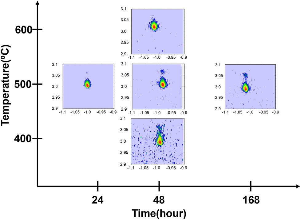 | ||
| Fig. 3 Dependence of the RSM on the annealing temperature and time in the 910 °C film. The RSM was measured along MgO[100] and [001]. The 206 peaks of T′ and C′ ZMGO were observed. | ||
Fig. 4 shows the TEM images for the annealed films whose RSM is similar to Fig. 3. The ZMGO film was deposited at a temperature of 840 °C and post-annealed at a temperature of 500 °C for 24 hours. It was confirmed that the RSM patterns before and after annealing were similar to those shown in Fig. 2(a) and 3. Fig. 4(a)–(c) show the tilted contrasts in addition to the columnar contrast. The electron diffraction pattern shows the C′ and T′ spots. The dark field image indicates that the tilted contrast is due to the T′ phase. The tilt angle from the surface normal is about 45°. The TEM image for another region is shown in Fig. 4(d)–(f). The tilt angle of the T′ domain from the surface normal is about 30° and 60°. The C′ phase exists throughout the film with a small portion of the T′ phase. The tilted nanostructure is usually not formed due to the growth geometric symmetry. Tilted nanostructures formed by the gradual variation of growth direction33 and miscut substrate34 have been reported. The present result indicates that the self-organization from the C′ template is a method to fabricate the tilted nanostructure.
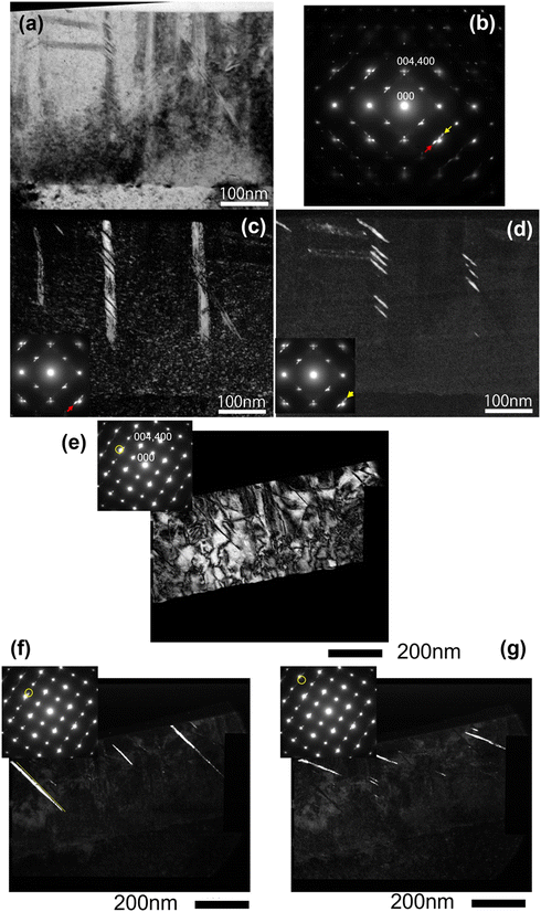 | ||
Fig. 4 TEM images for the annealed ZMG/MgO film containing C′ and T′ phases. The region for (a)–(d) is different from that for (e)–(g). (a) and (c)–(g) show the bright field and dark field images. (b) shows the electron diffraction pattern. The dark field images were obtained by diffraction, indicated by the arrow in the inset. In (b), (c), and (d), the arrows show ![[4 with combining macron]](https://www.rsc.org/images/entities/char_0034_0304.gif) 04 and 40 spots of T′. While the yellow circles in (e) and (f) show 04 of C′, the yellow circles in (f) and (g) show 40 and 08 of T′, respectively. 04 and 40 spots of T′. While the yellow circles in (e) and (f) show 04 of C′, the yellow circles in (f) and (g) show 40 and 08 of T′, respectively. | ||
B. Formation of an in-plane one dimensional structure in ZMGO/MgO/STO
Fig. 5(a) shows the 2θ − ω scan result for the as-deposited ZMGO film directly on an STO substrate for substrate temperatures of 840 °C and 910 °C. The ZMGO 111 and 222 peaks are observed for the substrate temperature of 840 °C. On the other hand, for the substrate temperature of 910 °C, the ZMGO 111 and 222 peaks are not observed, and a weak ZMGO 004 peak is observed. Due to a large lattice mismatch, the epitaxial growth of ZMGO is not dominant on STO. | ||
| Fig. 5 2θ − ω scan result for (a) ZMGO/STO and (b) ZMGO/MgO/STO. The right panels show the enlarged view of the left panels. | ||
The crystalline structures of ZMGO and STO are spinel and perovskite, respectively, and the lattice mismatch between ZMGO and STO is 0.10. Although the crystalline structure of MgO is rock salt, epitaxial ZMGO/MgO was fabricated due to a small lattice mismatch of 0.01 as shown in Fig. 2. The large lattice mismatch and different crystalline structure of STO suppress the (001) oriented growth of ZMGO. Therefore, an MgO buffer layer was fabricated on STO substrates to prepare epitaxial ZMGO. Fig. 5(b) shows the 2θ − ω scan result of MgO/STO. The MgO 200 peak is observed, indicating the growth of MgO on STO with the orientation relationship of MgO(100)//STO(100).
Fig. 5(b) shows the deposition temperature dependence of the 2θ − ω scan result. The ZMGO 004 peak is observed on MgO/STO, indicating the (001) oriented growth of ZMGO on the MgO/STO. The T′ phase with a large c-axis length is observed for a deposition temperature of 575 °C, while the C′ phase with a small c-axis length is observed for deposition temperatures higher than 840 °C. The deposition temperature of 785 °C is an intermediate condition, resulting in the formation of both T′ and C′. This is reasonable because T′ and C′ appear at moderate and high temperatures according to the phase diagram in Fig. 1.
Fig. 6 shows the dependence of the RSM on the deposition temperature for the as-deposited ZMGO/MgO/STO samples. In addition to the STO 103 and STO 113 peaks, the ZMGO peak is observed. While the MgO 113 peak overlaps with the ZMGO 226 peak for the STO[110] direction, only the ZMGO peak is observed for the STO[100] direction since MgO 103 is not observed. 3H > L at the peak for the deposition temperature of 785 °C and 575 °C, indicating T′-ZMGO. 3H = L for the deposition temperature of 870 °C indicates C′-ZMGO. The RSM along STO[100] for intermediate deposition temperatures of 785 °C and 840 °C exhibits an X-shaped ZMGO peak, indicating a mixture of T′-ZMGO and C′-ZMGO and diffuse scattering.
 | ||
| Fig. 6 RSM results for the ZMGO/MgO/STO films deposited at 575–870 °C. The vertical axis is along STO[001]. In upper and lower panels, the horizontal axis is along STO[100] and STO[100], respectively. The reciprocal lattice unit is defined according to the STO lattice parameter. The upper left panel shows the schematic illustration of the twin domain structure. | ||
Fig. 7 shows the TEM image of the non-annealed ZMGO film. There is a defective MgO buffer layer between the substrate and the film, which will be more clearly confirmed by EDX in Fig. 8. Defects spreading in the 45° direction are observed. The electron diffraction pattern shows the main spot and the streak. The streak shows twin domains spreading in the 45° tilted direction. Fig. 7(c)–(f) show the TEM images for another region of the same film. The dark field images also show that the defects are twin boundaries. The size and spacing of the twin domains are ∼10 nm. The observed twin domains are significantly different from the twin distribution in ZMGO/MgO.
 | ||
| Fig. 7 (a)–(c) The TEM images for non-annealed ZMGO/MgO/STO, and (d)–(f) those for a different region of the same film. While (a) and (c) show the bright field image, (b) and (d) show the electron diffraction pattern. (e) and (f) show the dark field image obtained using spots A and B in (d), respectively. In (d), A and B show 40 of (001)-oriented T′ and 04 of (100)-oriented T′. | ||
 | ||
| Fig. 8 EDX result for Zn, Mn, Ga, and Mg. The scale bar is 200 nm. | ||
Fig. 8 shows the EDX image of the same film as that in Fig. 7. Mg is localized at the interface between the film and the substrate, indicating the MgO buffer layer with a thickness of ∼50 nm. In the ZMGO layer, the compositional distribution of Zn, Mn, and Ga is homogeneous, indicating the ZMGO single phase with no phase separation. Zn, Mn, and Ga are also distributed in the MgO buffer layer. Thus, Zn, Mn, and Ga may be substituted in the MgO buffer.
The ZMGO/MgO/STO films were annealed, and the RSM results along STO[100] are shown in Fig. 9. While the intensity of the T′ phase decreases after annealing, the C′ phase disappears after 400 °C annealing and survives after 500–600 °C annealing. This is reasonable because C′ is stable at high temperature. Fig. 9(b) shows the dependence of 2θ − ω scan results on the annealing time at an annealing temperature of 500 °C. The non-annealed film exhibits the T′ and C′ peaks, which is consistent with the RSM result. While the T′ peak decreases with increasing annealing time, the C′ peak is unchanged after the annealing.
 | ||
| Fig. 9 (a) Dependence of the RSM on the annealing temperature and annealing time. The RSM surrounded by the solid line square is the RSM for the non-annealed film. (b) 2θ − ω scan result for the ZMG/MgO/STO films annealed for 6, 24, and 48 hours at an annealing temperature of 500 °C. | ||
Fig. 10 shows the TEM images of ZMGO/MgO/STO annealed at 500 °C for 6 hours. The bright field and dark field images show an elongated contrast along the surface and an ordered checkerboard contrast. The ordered checkerboard contrast is not the twin domains in the non-annealed film observed in Fig. 7, suggesting a structural change due to the annealing. The ordered checkerboard contrast is similar to the in-plane structure in ZMGO/MgO, namely the NCB,29,30 which is formed by annealing the twin domains. To confirm the NCB formation, the compositional distribution should be discussed because the NCB consists of T-ZMGO and C-ZMGO with different Zn/Mn ratios. Fig. 10(c) shows the compositional distribution of Ga and Mn. The ordered checkerboard consists of the nanoscale T phase with rich Mn (poor Ga) and the nanoscale C phase with rich Ga (poor Mn). The nanostructure formation mechanism has been discussed based on phase separation.35,36 Thus, the TEM observation demonstrates the NCB. Fig. 10(a) shows the schematic illustration of the structure of annealed ZMGO/MgO/STO. The elongated contrast along the surface and the ordered checkerboard contrast are the NCB in the side and top views, respectively.
 | ||
| Fig. 10 (a) Bright field and (b) dark field images for annealed ZMGO/MgO/STO. The inset of (a) shows the enlarged view of the checkerboard contrast. The inset of (b) shows the electron diffraction pattern and the schematic illustration of the structure. (c) EDX result of Ga and Mn for the checkerboard contrast. | ||
4. Discussion
A. Difference in the twin template between MgO and MgO/STO
Here, the difference in the film structure between ZMGO/MgO and ZMGO/MgO/STO is discussed. The bonding nature of the interface is the same, but the thickness of the MgO layer is different. The strain is an important factor to discuss the structural evolution in self-organization.37–40 The MgO thickness is 500 μm for the substrate and 50 nm for the buffer layer, a difference of four orders of magnitude. The force balance for the film and the strain relationship to accommodate the lattice mismatch are described as follows:41| EZMGOεZMGOtZMGO = EMgOεMgOtMgO |
| εZMGO + εMgO = f |
Here, E, ε, t, and f are the Young's modulus, elastic strain, thickness, and elastic component of lattice mismatch, respectively. tZMGO is 370 nm according to the TEM images. The thickness difference between the MgO buffer (50 nm) and the MgO substrate (500 μm) is 4 orders of magnitude. Compared with the thickness difference, the influence of the Young's modulus difference is weak. Here, we can assume EZMGO = EMgO to discuss the influence of the thickness on the elastic strain. In the case of the MgO substrate, εZMGO = f and εMgO = 0. On the other hand, in the case of the MgO buffer layer, εZMGO = 0.12f and εMgO = 0.88f. This indicates that the MgO substrate induces significant stress in the ZMGO films, while the stress effect of the MgO buffer layer is weak. In ZMGO/MgO, the MgO substrate forms an epitaxial ZMGO layer with the same lattice parameters as MgO, which induces shear stress in the ZMGO films. On the other hand, the stress is not applied or weak in the ZMGO films on MgO/STO, resulting in free deformation of ZMGO. Fig. 11 shows the surface view of the ZMGO lattice. While the MgO lattice parameter is 4.213 Å, the a-axis and c-axis lengths for T′ ZMGO are 8.21 and 8.79 Å, respectively. The epitaxial stress from the MgO substrate expands the C′ lattice to the epitaxial T′ ZMGO layer. The shear stress forms a/c or c/a domains and then vertical twin domains. On the other hand, C′ ZMGO is freely deformed into T′ ZMGO, forming a/c, c/a, and a/a domains. To configure the a/c, c/a, and a/a domains in the film, tilted twin boundaries extending to the 45° tilted direction are formed. Thus, the stress from MgO affects the twin domain orientations observed in the present study.
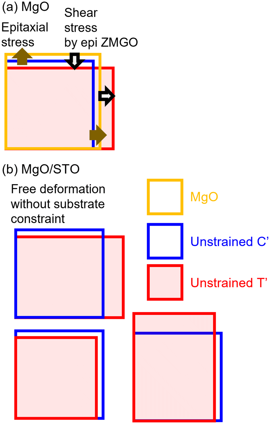 | ||
| Fig. 11 Surface views of the lattice of C′ ZMGO and T′ ZMGO for (a) ZMGO/MgO and (b) ZMGO/MgO/STO. In (a), the C′ lattice is strained by MgO as shown by the solid arrows so that the C′ lattice matches with the MgO lattice. The strained C′ lattice relaxes under the shear stress to form twin domains as shown by the open arrows. | ||
B. T′ domain formation from C′
According to the near coincidence site lattice model,42,43 the highly symmetric plane forms an interface, and the lattice mismatch should be small. In addition, the equivalent planes of T′ and C′ should face the interface because the atomic configuration is almost the same. Fig. 12 shows the lattices of C′ and T′ ZMGO from the surface view. Here, the lattice parameters for C′ and T′ are denoted by aC′, and aT′ and cT. aT′ = 8.21 Å, cT′ = 8.79 Å, and aC′ = (aT′ × aT′ × cT′)1/3 = 8.40 Å. The lattice mismatches between aC′ and aT′ and between aC′ and cT′ are −0.02 and 0.05. The lattice mismatch between [110](C′) and [110](T′) is 0.013 and the angle between [110](T′) and [100](T′) is 47.0°. In addition, the lattice mismatches between [120](C′) and [120](T′) and between [120](C′) and [210](T′) are 0.032 and −0.0083. The angle between [210](T′) and [100](T′) is 26.6°. These angles explain the elongated direction of the tilted T′ domain observed by TEM. Because the lattice mismatch is smaller for [210](T′), namely the angle of 26.6°, the domains for this configuration were wider than the interface of [110](T′) and the angle of ∼45° in Fig. 4(e)–(g). | ||
| Fig. 12 Lattice of C′ and T′ ZMGO to form the tilted T′ domain in the C′ phase. The lattice in the cross-section of the films is shown. The solid lines are possible directions to form the interface. | ||
The asymmetric self-organization in ZMGO/MgO/STO is explained by the direction of the twin domain dominated by strain. The T′ phase formation tilted from the vertical or in-plane directions is discussed based on the orientation relationship at the interface of C′/T′. The twin domain (T′/T′) and the phase domain (C′/T′) are tilted from the direction vertical or parallel to the film/substrate interface due to strain or substrate constraints, leading to asymmetric self-organization. The thermodynamic, interface, and strain energies and phase formation kinetics need to be discussed to quantitatively clarify the detailed mechanism.
C. Possible applications
(Co,Mn,Fe)3O4 (CMFO) shows the same phase separation. CMFO is a magnetic material,44 and the magnetic properties can be controlled by the demagnetization effect determined by the shape. The demagnetization is weak in the elongated direction, but strong in the thin direction. This study demonstrates that the direction of domain spreading is in-plane, tilted from the surface, and vertical depending on the substrate and the deposition temperature. Thus, the magnetic properties are changed by the structure, which should be discussed in the future. The present conclusion is fundamental to structural control in the CFMO film, and ZMGO can be used as a buffer layer for CFMO films.5. Conclusion
The phase separation in ZMGO films was controlled through the template to break self-organization along the symmetric direction. ZMGO/MgO films were mainly the C′ phase when they were deposited at high temperature. Upon annealing the C′ film, the XRD pattern of the C′ phase is not so significantly changed. TEM shows that the nanoscale T′ domains spread in the tilted direction from the surface, which is determined by lattice mismatch, lattice symmetry, and atomic bonding. The tilted twin domains were formed on the MgO-buffered STO substrate, which does not apply strong stress to the ZMGO layer. By annealing the ZMGO/MgO/STO films, an in-plane aligned NCB was fabricated. The in-plane spreading is difficult in conventional self-organization and was successfully achieved by phase separation type self-organization in the ZMGO films with a controlled template. These nanostructures are significantly different from the typical structure of a vertically aligned NCB, which is dominated by epitaxial strain. This study demonstrates the possibility of fabricating a nanostructure that breaks growth geometric symmetries, opening complicated three-dimensional structures by self-organization.Author contributions
T. H. conceptualized the research, designed the experiment and analysis, and wrote the manuscript. M. U. and T. H. prepared the samples and performed XRD. M. U. and Y. H. performed TEM. M. I. prepared the TEM specimen and performed TEM. All authors discussed the results.Data availability
The data supporting this article have been included in this article.Conflicts of interest
There are no conflicts to declare.Acknowledgements
This work was partially supported by the Grant-in-Aid for Challenging Research (Exploratory) (24K21687).References
- H. Hoffmann and F. Steinbauer, Single domain and vortex state in ferromagnetic circular nanodots, J. Appl. Phys., 2002, 92, 5463–5467 CrossRef CAS.
- S. X. Guan, T. H. Yang and C. H. Yang, et al., Monolithic 3D integration of back-end compatible 2D material FET on Si FinFET, npj 2D Mater. Appl., 2023, 7, 9 CrossRef CAS.
- G. Blatter, M. V. Feigel'man, V. B. Geshkenbein, A. I. Larkin and V. M. Vinokur, Vortices in high-temperature superconductors, Rev. Mod. Phys., 1994, 66, 1125–1388 CrossRef CAS.
- X. Obradors and T. Puig, Coated conductors for power applications: Materials challenge, Supercond. Sci. Technol., 2014, 27, 044003 CrossRef CAS.
- K. Biswas, J. He and I. Blum, et al., High-performance bulk thermoelectrics with all-scale hierarchical architectures, Nature, 2012, 489, 414–418 CrossRef CAS.
- Z. Chen, X. Zhang and Y. Pei, Manipulation of phonon transport in thermoelectrics, Adv. Mater., 2018, 30, 1705617 CrossRef.
- M. Wang, B. A. Muhich, Z. He, Z. Yang, D. Yang, M. Lucero, H. K. K. Nguyen, G. E. Sterbinsky, L. Árnadóttir, H. Zhou, L. Fei and Z. Feng, Metal Doping Regulates Electrocatalysts Restructuring During Oxygen Evolution Reaction, ChemSusChem, 2024, 17, e202400332 CrossRef CAS PubMed.
- W.-S. Lin, M. Rinawati, W.-H. Huang, C.-Y. Chang, L.-Y. Chang, Y.-S. Cheng, C.-C. Chang, J.-L. Chen, W.-N. Su and M.-H. Yeh, Surface Restructuring Prussian Blue Analog-Derived Bimetallic CoFe Phosphides by N-Doped Graphene Quantum Dots for Electroactive Hydrogen Evolving Catalyst, J. Colloid Interface Sci., 2024, 654(Part A), 677–687 CrossRef CAS PubMed.
- S. Subhadarshini, E. Pavitra, G. S. R. Raju, N. R. Chodankar, D. K. Goswami, Y.-K. Han, Y. S. Huh and N. Ch. Das, One-Dimensional NiSe–Se Hollow Nanotubular Architecture as a Binder-Free Cathode with Enhanced Redox Reactions for High-Performance Hybrid Supercapacitors, ACS Appl. Mater. Interfaces, 2020, 12, 29302–29315 CAS.
- A. Chen, Q. Su, H. Han, E. Enriquez and Q. Jia, Metal oxide nanocomposites: A perspective from strain, defect, and interface, Adv. Mater., 2019, 31, 1803241 CrossRef PubMed.
- J. L. MacManus-Driscoll, Self-assembled heteroepitaxial oxide nanocomposite thin film structures: Designing interface-induced functionality in electronic materials, Adv. Funct. Mater., 2010, 20, 2035 CrossRef CAS.
- H. Zheng, J. Wang, S. E. Lofland, Z. Ma, L. M. Ardabili, T. Zhao, L. S. Riba, S. R. Shinde, S. B. Ogale and F. Bai, Multiferroic BaTiO3-CoFe2O4 nanostructures, Science, 2004, 303, 661–663 CrossRef CAS.
- J. L. Macmanus-Driscoll, S. R. Foltyn, Q. Jia, H. Wang, A. Serquis, L. Civale, B. Maiorov, M. E. Hawley, M. P. Maley and D. E. Peterson, Strongly enhanced current densities in superconducting coated conductors of YBa2Cu3O7−x + BaZrO3, Nat. Mater., 2004, 3, 439–443 CrossRef CAS.
- A. Goyal, S. Kang, K. J. Leonard, P. M. Martin, A. A. Gapud, M. Varela, M. Paranthaman, A. O. Ijaduola, E. D. Specht and J. R. Thompson, Irradiation-free, columnar defects comprised of self-assembled nanodots and nanorods resulting in strongly enhanced flux-pinning in YBa2Cu3O7−δ films, Supercond. Sci. Technol., 2005, 18, 1533–1538 CrossRef CAS.
- A. Xu, L. Delgado, N. Khatri, Y. Liu, V. Selvamanickam, D. Abraimov, J. Jaroszynski, F. Kametani and D. C. Larbalestier, Strongly enhanced vortex pinning from 4 to 77 K in magnetic fields up to 31 T in 15 mol% Zr-added (Gd,Y)-Ba-Cu-O superconducting tapes, APL Mater., 2014, 2, 046111 CrossRef.
- T. Horide, N. Matsukida, M. Ishimaru, R. Kita, S. Awaji and K. Matsumoto, Pin potential effect on vortex pinning in YBa2Cu3O7−δ films containing nanorods: Pin size effect and mixed pinning, Appl. Phys. Lett., 2017, 110, 052601 CrossRef.
- F. Rizzo, A. Augieri, A. A. Armenio, V. Galluzzi, A. Mancini, V. Pinto, A. Rufoloni, A. Vannozzi, M. Bianchetti, A. Kursumovic, J. L. MacManus-Driscoll, A. Meledin, G. V. Tendeloo and G. Celentano, Enhanced 77 K vortex-pinning in YBa2Cu3O7−x films with Ba2YTaO6 and mixed Ba2YTaO6 + Ba2YNbO6 nano-columnar inclusions with irreversibility field to 11 T, APL Mater., 2016, 4, 061101 CrossRef.
- S. A. Harrington, J. Zhai, S. Denev, V. Gopalan, H. Wang, Z. Bi, S. A. T. Redfern, S. H. Baek, C. W. Bark and C. B. Eom, Thick lead-free ferroelectric films with high Curie temperatures through nanocomposite-induced strain, Nat. Nanotechnol., 2011, 6, 491–195 CrossRef CAS.
- S. M. Yang, S. Lee, J. Jian, W. Zhang, P. Lu, Q. Jia, H. Wang, T. W. Noh, S. V. Kalinin and J. L. MacManus-Driscoll, Strongly enhanced oxygen ion transport through samarium-doped CeO2 nanopillars in nanocomposite films, Nat. Commun., 2015, 6, 8588 CrossRef CAS.
- T. Horide, H. Katagiri, A. Ichinose and K. Matsumoto, Fabrication of Fe(Te,Se) films added with oxide or chalcogenide: Influence of added material on phase formation and superconducting properties, J. Appl. Phys., 2022, 131, 103901 CrossRef CAS.
- M. Ogata, K. Kadowaki, M. Ijiri, Y. Takemoto, K. Terashima, T. Wakita, T. Yokoya and Y. Muraoka, Effect of aliovalent dopants on the kinetics of spinodal decomposition in rutile-type TiO2-VO2, J. Eur. Ceram. Soc., 2017, 37, 3177–3183 CrossRef CAS.
- T. Teranishi, H. Matsui, S. Kondo and A. Kishimoto, Spinodal decomposition-derived giant polarization in TiO2−SnO2 generated from a metastable phase, J. Appl. Phys., 2023, 133, 174101 CrossRef CAS.
- Y. Li, X. Wang, Y. Shao, D. Tang, B. Wu, Z. Tang and W. Lin, Stability and spinodal decomposition of the solid-solution phase in the ruthenium–cerium–oxide electro-catalyst, Phys. Chem. Chem. Phys., 2015, 17, 1156–1164 RSC.
- P. Zajdel, P.-Y. Hsieh, E. E. Rodriguez, N. P. Butch, J. D. Magill, J. Paglione, P. Zavalij and M. R. Suchomel, Phase separation and suppression of the structural and magnetic transitions in superconducting doped iron tellurides, Fe1+xTe1−ySy, J. Am. Chem. Soc., 2010, 132, 13000–13007 CrossRef CAS PubMed.
- T. Horide, A. Ichinose, M. Tanaka and K. Matsumoto, Observation of anion-stoichiometry phase separation in Fe(Te,Se) film, J. Appl. Phys., 2023, 133, 203903 CrossRef CAS.
- S. Yeo, Y. Horibe, S. Mori, C. M. Tseng, C. H. Chen, A. G. Khachaturyan, C. L. Zhang and S. W. Cheong, Solid state self-assembly of nanocheckerboards, Appl. Phys. Lett., 2006, 89, 233120 CrossRef.
- C. L. Zhang, C. M. Tseng, C. H. Chen, S. Yeo, Y. J. Choi and S. W. Cheong, Magnetic nanocheckerboards with tunable sizes in the Mn-doped CoFe2O4 spinel, Appl. Phys. Lett., 2007, 91, 233110 CrossRef.
- C. L. Zhang, S. Yeo, Y. Horibe, Y. J. Choi, S. Guha, M. Croft, S. W. Cheong and S. Mori, Coercivity and nanostructure in magnetic spinel Mg(Mn,Fe)2O4, Appl. Phys. Lett., 2007, 90, 133123 CrossRef.
- S. Park, Y. Horibe, T. Asada, L. S. Wielunski, N. Lee, P. L. Bonanno, S. M. O'Malley, A. A. Sirenko, A. Kazimirov and M. Tanimura, Highly aligned epitaxial nanorods with a checkerboard pattern in oxide films, Nano Lett., 2008, 8, 720–724 CrossRef CAS PubMed.
- T. Horide, K. Morishita, Y. Horibe, M. Usuki, M. Ishimaru and K. Matsumoto, Aligned self-organization induced by epitaxial stress and shear deformation in Jahn–Teller spinel ZnMnGaO4, J. Phys. Chem. C, 2022, 126, 806–814 CrossRef CAS.
- M. Kornbluth and C. A. Marianetti, Origin of spinel nanocheckerboards via first principles, Phys. Rev. Lett., 2015, 114, 226102 CrossRef.
- S. M. O'Malley, P. L. Bonanno, K. H. Ahn, A. A. Sirenko, A. Kazimirov, M. Tanimura, T. Asada, S. Park, Y. Horibe and S. W. Cheong, Epitaxial checkerboard arrangement of nanorods in ZnMnGaO4 films studied by X-ray diffraction, Phys. Rev. B:Condens. Matter Mater. Phys., 2008, 78, 165424 CrossRef.
- M. Mukaida, A. Ichinose, P. Mele, K. Matsumoto, S. Horii and Y. Yoshida, Phys. Procedia, 2012, 36, 1631–1636 CrossRef CAS.
- F. J. Baca, P. N. Barnes, R. L. S. Emergo, T. J. Haugan, J. N. Reichart and J. Z. Wu, Control of BaZrO3 nanorod alignment in YBa2Cu3O7−x thin films by microstructural modulation, Appl. Phys. Lett., 2009, 94, 102512 CrossRef.
- Y. Ni, W. Rao and A. G. Khachaturyan, Pseudospinodal mode of decomposition in films and formation of chessboard-like nanostructure, Nano Lett., 2009, 9, 3275–3281 CrossRef CAS PubMed.
- Y. Ni and A. G. Khachaturyan, Mechanism and conditions of the chessboard structure formation, Acta Mater., 2008, 56, 4498–4509 CrossRef CAS.
- Q. Xie, A. Madhukar, P. Chen and N. P. Kobayashi, Vertically self-organized InAs quantum box islands on GaAs(100), Phys. Rev. Lett., 1995, 75, 2542 CrossRef CAS PubMed.
- G. Springholz, M. Pinczolits, P. Mayer, V. Holy, G. Bauer, H. H. Kang and L. T. Salamanca-Riba, Tuning of vertical and lateral correlations in self-organized PbSe/Pb1−xEuxTe quantum dot superlattices, Phys. Rev. Lett., 2000, 84, 4669 CrossRef CAS PubMed.
- J. L. Macmanus-Driscoll, P. Zerrer, H. Wang, H. Yang, J. Yoon, A. Fouchet, R. Yu, M. G. Blamire and Q. Jia, Strain control and spontaneous phase ordering in vertical nanocomposite heteroepitaxial thin films, Nat. Mater., 2008, 7, 314–320 CrossRef CAS PubMed.
- T. Horide, F. Kametani, S. Yoshioka, T. Kitamura and K. Matsumoto, Structural evolution induced by interfacial lattice mismatch in self-organized YBa2Cu3O7−δ nanocomposite film, ACS Nano, 2017, 11, 1780–1788 CrossRef CAS PubMed.
- T. Horide, T. Maekawa, T. Aikawa, T. Kitamura and K. Nakamura, Tc and resistivity variation induced by external bending strain in flexible film of strain-sensitive (La,Sr)2CuO4, Phys. Rev. Mater., 2024, 8, 094802 CrossRef CAS.
- T. Horide, K. Hara and K. Matsumoto, Fabrication of Y doped BaZrO3 epitaxial film on YBa2Cu3Ox sacrificial buffer layer, Thin Solid Films, 2016, 598, 25–32 CrossRef CAS.
- S. W. Chan, Degenerate epitaxy, coincidence epitaxy and origin of ‘special’ boundaries in thin films, J. Phys. Chem. Solids, 1994, 55, 1137–1145 CrossRef CAS.
- Y. Horibe, M. Ishimatsu, S. Takeyama, S. Mori, M. Kudo, M. Auchi, M. Tanaka and Y. Murakami, Self-assembled lamellar-type nanostructure in manganite spinel (Co,Mn,Fe)3O4, Appl. Phys. Lett., 2019, 115, 232401 CrossRef.
| This journal is © The Royal Society of Chemistry 2025 |