
 Open Access Article
 This Open Access Article is licensed under a
 Creative Commons Attribution 3.0 Unported Licence
Conformal chemical vapor deposition of B4C thin films onto carbon nanotubes†
Arun Haridas
Choolakkal
 a,
Ingemar
Persson
a,
Jarkko
Etula
b,
Emma
Salmi
b,
Taneli
Juntunen
b,
Per O. Å.
Persson
a,
Jens
Birch
a and
Henrik
Pedersen
*a
a,
Ingemar
Persson
a,
Jarkko
Etula
b,
Emma
Salmi
b,
Taneli
Juntunen
b,
Per O. Å.
Persson
a,
Jens
Birch
a and
Henrik
Pedersen
*a
aDepartment of Physics, Chemistry and Biology, Linköping University, SE-581 83 Linköping, Sweden. E-mail: henrik.pedersen@liu.se
bCanatu, Tiilenlyöjänkuja 9A, FI-01720 Vantaa, Finland
First published on 3rd February 2025
Abstract
The unique attributes of carbon nanotubes (CNTs) establish them as the preferred material for fabricating sophisticated membrane architectures. However, CNT membranes are also susceptible to degradation under harsh environmental conditions, necessitating protective measures to maintain their functionalities. This study presents deposition of boron carbide (B4C) thin films as protective coatings on CNT membranes using chemical vapor deposition. Electron microscopy shows that B4C films were uniformly deposited on the CNTs. Raman spectroscopy shows the preservation of the G and D bands, with a notable stability in the RBM bands, while XPS measurements show sp2 hybridized C–C bonds and an additional shoulder characteristic of the deposited B4C film. This suggests that the CVD process does not degrade the CNTs, but merely adds a layer of B4C to their outer surface. This deposition process also allows for precise control over the membrane's pore size, offering the potential to fine-tune the properties of CNT membranes.
1. Introduction
Carbon nanotubes (CNTs) are cylindrical structures made of sp2-bonded carbon atoms with diameters ranging from 0.7 to 100 nm and lengths of up to several micrometers.1–3 CNT membranes consist of aligned or randomly oriented CNTs forming a network of nanopores that enables selective transport or filtration of particles.4–6 CNT membranes have several advantages over conventional membranes, such as high permeability, low fouling, high thermal and mechanical stability, and tunable selectivity.7,8 They have attracted considerable attention for various applications, such as water treatment,9 desalination,10,11 chemical separation,12 and energy storage.13 However, CNT membranes are also susceptible to environmental degradation, such as plasma induced damage, chemical degradation, or microbial growth which can compromise their performance and durability, especially in harsh environments.5,14,15 Degradation can lead to changes in the effective pore size or changes to other properties of the membrane.5,15One possible way to protect CNTs from external damage and improve their performance is to coat various materials onto CNTs that can enhance their durability and functionality in harsh environments.5,14,16,17 For example, coating with metal oxides such as TiO2, Al2O3, ZnO, or NiCoO2 onto CNTs can enhance their anti-fouling and anti-oxidation capabilities, as well as impart photocatalytic, hydrophobic or electrochemical properties.18–23 Depositing polymer layers can modify the electrical and thermoelectric properties, and it also holds promise for biotechnological applications.24–26 Deposition of nanomaterials, such as graphene, gold, nanodiamond, or fullerene, can enhance the photoelectrical, electrical, thermal, and mechanical properties of CNTs, and enable new applications, such as sensors, electromagnetic shields, electrodes, or electrochemical material.27–30
Although capping or surface modification of CNTs with thin films or nanoparticles of various materials has been proposed to protect and functionalize CNTs, depositing materials uniformly around CNTs in a free-standing membrane structure is challenging due to their highly complex 3D morphology. The thickness of the deposition must be meticulously regulated to ensure that the CNT pores remain unobstructed and to achieve uniform surface coverage. The standard film deposition technique for highly conformal thin film deposition onto topographically complex surfaces is atomic layer deposition (ALD),31,32 which is based on sequential, self-limiting surface chemical reactions.
Due to its high hardness, high thermal stability, high chemical resistance, and low-density,33 boron carbide stands out as a material of great interest for encapsulating carbonaceous materials. It has been reported that thin film deposition of boron carbide can improve the chemical stability of graphite films,34 even in plasma facing components for nuclear application.35 But deposition of boron carbide thin films by ALD is difficult to realize due to the limited number of precursor chemistries that exhibit self-limiting surface chemistry to deposit carbides by ALD. In this study, we explore the potential application of a recently developed chemical vapor deposition (CVD) process36 for boron carbide (B4C) thin films onto CNTs in a membrane structure. By using triethyl boron as a single source CVD precursor and Xe as a diffusion additive we demonstrate highly conformal deposition of B4C thin film onto CNTs with various diameters arranged randomly in a free-standing membrane structure. This method also illustrates the capacity of the CVD process to fine-tune the pore dimensions within the composite membrane.
2. Experimental
2.1. Deposition process
The thermal CVD process was carried out in a horizontal hot-wall CVD reactor. Semiconductor-grade triethylboron (TEB, B(C2H5)3) from SAFC Hitech was employed as the single-source precursor and palladium membrane-purified hydrogen gas (H2) served as both a carrier gas and a co-reactant. To maintain stable precursor delivery, TEB was stored in a stainless-steel bubbler within a thermostat bath at 0 °C, maintaining a vapor pressure of approximately 1.65 kPa. This stability was achieved by bubbling hydrogen gas through the liquid TEB. Additionally, a co-flow of xenon (Xe) (99.998%) was introduced as a diffusion additive. Deposition without added Xe rendered less conformal coating on the CNTs. Thin films were deposited on both CNT membranes, consisting of randomly arranged few-walled carbon nanotubes with various diameters supplied by Canatu,37,38 and polished Si(100) substrates for reference samples. The CNTs were in the form of a free-standing membrane stretched over a quartz frame giving a total area of about 25 × 25 mm. The CNT membranes were used as received. For reference experiments, 10 × 10 mm Si substrates were washed in an ultrasonic bath in acetone and ethanol for 3 minutes and then blow-dried with nitrogen gas. CNT membranes or Si substrates were loaded into a SiC-coated graphite susceptor in the CVD reactor. The reactor was evacuated, backfilled with hydrogen gas (H2), and heated to deposition temperature, 550 °C, under a 2000 sccm flow of H2 at 5 kPa, regulated by a throttle valve on the process pump. The temperature was stabilized for 5 minutes at the deposition temperature before initiating the deposition process by introducing TEB into the reactor. A flow of 1 sccm of TEB, resulting in a partial pressure of 1.18 Pa, was used along with 100 sccm of xenon (Xe), achieving a partial pressure of 18 Pa. The total pressure was maintained at 5 kPa for the deposition.2.2. Characterization
Scanning transmission electron microscopy (TEM) was carried out using the Linköping double corrected and monochromated FEI Titan3 60–300 (S)TEM equipped with a high brightness Schottky field emission gun (XFEG) and operated at 300 kV. The achieved resolution was measured to 0.7 Å on a Au/Pd nanoparticle reference grating. A Wien type monochromator was used to control the beam current to 40 pA. Electron energy-loss spectroscopy (EELS) mapping was performed using a Gatan GIF Quantum ERS 966 dual EELS spectrometer with 1.2 eV energy resolution in non-monochromated mode at 300 kV and at 0.25 eV dispersion. DualEELS mapping was carried out using high speed acquisition mode to limit the dose. Scanning TEM (STEM) images were acquired with an annular dark field (ADF) detector using a 21.5 mrad convergence semi-angle and with a camera length corresponding to 60–180 mrad collection angles. STEM cross-section samples were prepared by delaminating membranes fixed to SiN frames in pure ethanol followed by float deposition on a Cu TEM ring. Image and spectrum processing was carried out using Gatan Microscopy Suite (GMS) 3.52 with licensed plugins for EELS spectrum imaging and elemental quantification. EELS quantification was carried out using the Hartree–Slater scattering cross-section model with low-loss corrected plural scattering deconvolution and near edge exclusion of 20 eV.X-ray reflectivity measurements were used to measure the thin film thickness on polished Si substrates and to calibrate the deposition process for depositing very thin and uniform films. The measurements were performed by utilizing Cu Kα radiation with the Cu Kβ component filtered out by a nickel filter. The data were recorded using an X'Pert MRD diffractometer with a 1/32° divergence slit and a 0.27° plate collimator, followed by analysis for film thickness and density using PANAlytical X'Pert Reflectivity software. A scanning electron microscope (SEM), specifically Zeiss Sigma 300 model was used to investigate the morphology of pristine and composite membranes. The in-lens secondary electron detector, with a 15 keV accelerating voltage and a 30 μm aperture, was used to micrograph the membranes. X-ray diffraction (XRD) analysis was conducted with a PANAlytical X'Pert Pro diffractometer. The incident beam side featured a Cu Kα X-ray source, which was outfitted with a Bragg–Brentano HD and had ½° divergence slit as primary optics. On the diffracted beam side, the apparatus includes an X'celerator detector that functioned in scanning mode, accompanied by a 5 mm antiscatter slit. The 002 peak of the diffraction curve was extracted, background subtracted and fitted with basic Gaussian function to estimate the full width at half maximum (FWHM).
X-ray photoelectron spectroscopy (XPS) was employed to investigate the chemical environment within the films using an AXIS Ultra DLD instrument from Kratos Analytical. The resulting data were analyzed using CasaXPS39 software. Given that the material was amorphous phase with the presence of amorphous carbon, the calibration was performed against the sp2 hybridized C–C peak position set at 284.5 eV. Time-of-flight elastic recoil detection analysis (ToF-ERDA) measurements were conducted on B4C film of 800 nm thickness deposited on Si substrate. The measurements were performed using 36 MeV Iodine (127I8+) ions as projectile beam and with a time-of-flight detector. The elemental composition was estimated by extracting the histograms and converting them into depth profile of elemental composition using Potku software.40
Raman spectroscopy measurements were conducted employing a 532 nm laser for excitation at 25 mW power, utilizing a ×60 objective lens. The spectral data were collected with an accusation time of 20 s and an accumulative average of 15 scans to avoid measurement artifacts and cosmic ray spikes. The spectra backgrounds were fitted with linear background and subtracted before the analysis. Some measurements were carried out on thick B4C film deposited on Si substrate. The known crystalline Si reference sample was used to calibrate the spectrum.
The high-resolution SEM micrographs were image-processed to analyze the porosity of the coated CNT membrane. Both pristine and CNTs with B4C films of various thicknesses were studied for comparison. The working distance, accelerating voltage, aperture, magnifications, brightness, and contrast of the micrographs were kept constant among the processed micrographs. A magnification of 100![[thin space (1/6-em)]](https://www.rsc.org/images/entities/char_2009.gif) 000-times was determined to be optimum for minimizing the position independent deviation from the average statistical distribution of the membrane features. Initially, the images were converted to gray scale and the contrasts of the images were normalized by linearly mapping the intensity values from 0 to 255. The number of depth levels were identified by analyzing the peaks in the histograms of the images. The pore distribution was mapped by processing the binarized micrographs using gradient magnitude, followed by watershed algorithms in Matlab, see the ESI† for details. The porosity was estimated by averaging the pixel intensity values of the gray scale depth mapped micrographs and expressed in 0 to 1 scale.
000-times was determined to be optimum for minimizing the position independent deviation from the average statistical distribution of the membrane features. Initially, the images were converted to gray scale and the contrasts of the images were normalized by linearly mapping the intensity values from 0 to 255. The number of depth levels were identified by analyzing the peaks in the histograms of the images. The pore distribution was mapped by processing the binarized micrographs using gradient magnitude, followed by watershed algorithms in Matlab, see the ESI† for details. The porosity was estimated by averaging the pixel intensity values of the gray scale depth mapped micrographs and expressed in 0 to 1 scale.
3. Results and discussion
Fig. 1a–c shows the morphology of a pristine CNT membrane, Fig. 1a shows a scanning electron microscopy (SEM) overview image of the CNT network and Fig. 1b present a magnified view showcasing the size distribution of pristine CNTs, Fig. 1c shows a high magnification scanning transmission electron microscopy (STEM) image detailing the structure of the CNT. An SEM overview and a high magnification SEM image of the CNT after 90 s CVD are shown in Fig. 1d and e, respectively. It can be noted that no clustering or nanoparticle formation can be seen at the intersections or in the pores, suggesting that the CVD chemistry is highly conformal. The SEM micrographs further reveal a flat membrane surface without any wrinkles, exhibiting no bowing or curvature caused by the CVD process. The film thickness appears to be uniform, regardless of nanotube diameter (Fig. 1d and e). However, for ultra-narrow tubes with a diameter of less than 2.5 nm, no deposition was observed. We ascribe this hindered nucleation of B4C films from TEB molecules to the inherent surface energy condition of ultra-narrow tubes, which is not favorable to the film formation.41,42Fig. 1f shows the corresponding high magnification STEM image of a single B4C coated CNT, indicating that it is possible the CNTs remain intact after the CVD process. STEM imaging at the present experimental conditions promote mass contrast (∼Z1.64). Hence, the lack of intensity in the core further suggests that it is possible the CNTs are intact. Fig. 1g and h shows the elemental distribution of B and C as captured from EELS elemental maps (employing the B–K and C–K edges), around CNTs, respectively. An EELS line scan (indicated by white arrows in the EELS maps) is presented in Fig. 1i, showing a B rich shell and C rich core.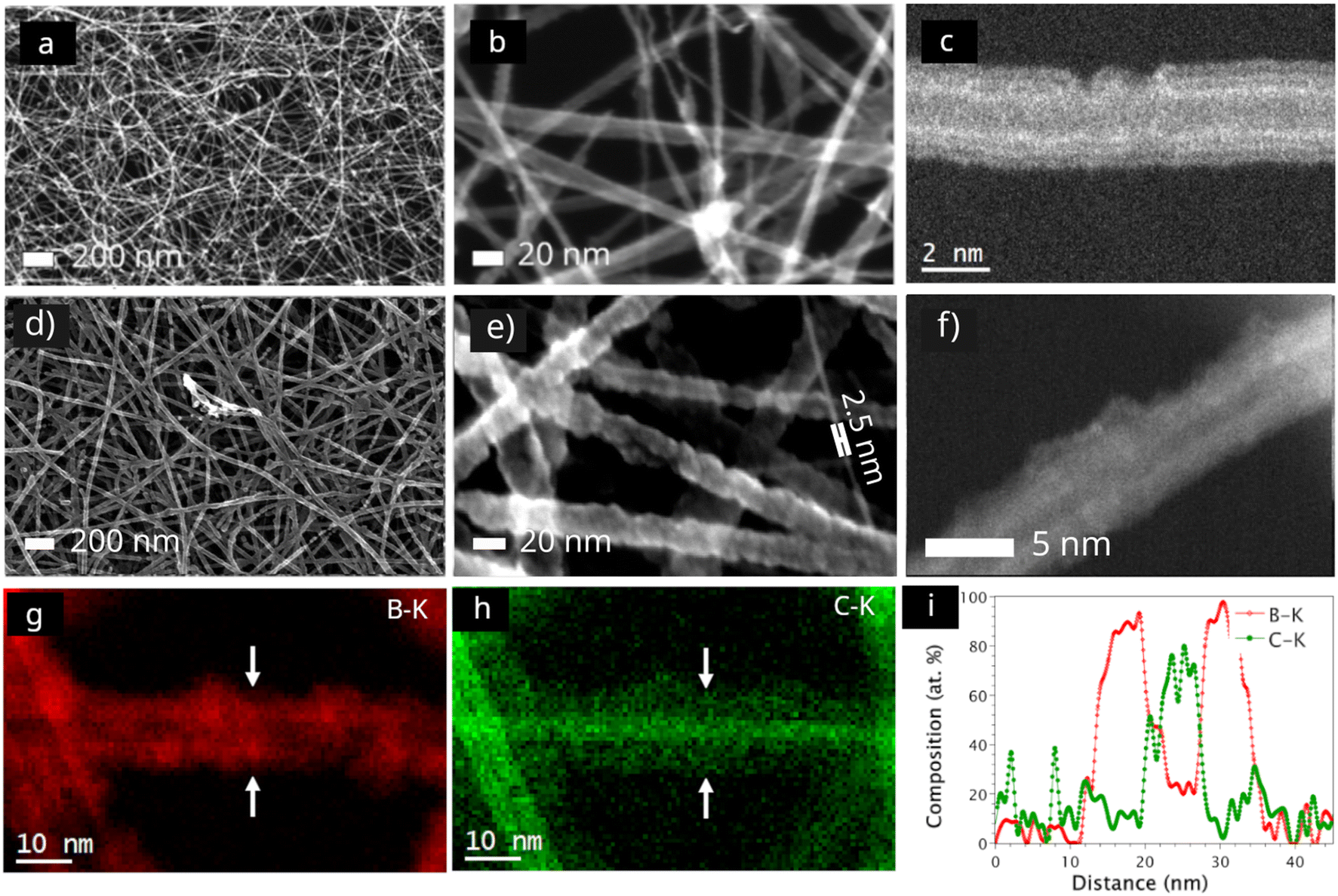 | ||
| Fig. 1 (a) and (b) SEM micrographs showing a pristine CNT membrane. (c) ADF STEM image of a single CNT. (d) and (e) SEM images showing uniform deposition of a thin film on the CNT membrane. (f) ADF STEM image showing a CNT after CVD. (g) EELS B–K map. (h) EELS C–K map. (i) EELS line scans across the B4C deposited CNT indicated by white arrows. | ||
XPS was used to analyze the chemistry of the B4C deposited CNTs. The pristine membrane exhibit an intense narrow peak at 284.5 eV attributed to sp2 hybridized C–C43 bonds (Fig. 2a). Additionally, a low intensity peak centered at 285.9 eV was assigned to C–O1,43 bonds. In contrast, the CNT membrane after CVD shows four distinct peaks (Fig. 2b). Major peaks centered at 284.6 eV, 283.3 eV and 282.4 eV were assigned to sp2 hybridized C–C bonds, C–B44 bonds (where sp2 hybridized carbon atoms are bonded to the equatorial B atoms in the icosahedra),45 and C atoms bonded to the sp hybridized B atoms in the C–B–C44 chains,45 respectively. Satellite peaks centered at 286 eV and 289 eV were assigned to C–O1,43 and O–C![[double bond, length as m-dash]](https://www.rsc.org/images/entities/char_e001.gif) O43 bonds, respectively. A shoulder can be observed below 284 eV, which arises from the deposited film where C was bonded to less electronegative B atoms. Further, broadening of the major peak centered at 284.5 eV indicates contribution from both the deposited film and the CNT underneath. We suggest that the differential charging of the membrane surfaces before and after CVD contributed to the broadening of the FWHM of sp2 hybridized C–C bond signals from 0.85 eV to 1.20 eV. The B 1s core level spectra shows three peak positions (Fig. 2c). While the major peak at 188.2 eV was assigned to the B–B46 bonds in the icosahedra structure,47 the peak centered at 188.8 eV was assigned to B–C44,46 bonds, and the minor peak at 190.6 eV was assigned to B–O44,46 bonds. The B rich B4C or B13C2 phases that form B icosahedra clusters connected by C–B–C linear chains,47,48 giving a higher intensity signal for B–B bonds compared to B–C bonds, is typical for B-rich carbide material.
O43 bonds, respectively. A shoulder can be observed below 284 eV, which arises from the deposited film where C was bonded to less electronegative B atoms. Further, broadening of the major peak centered at 284.5 eV indicates contribution from both the deposited film and the CNT underneath. We suggest that the differential charging of the membrane surfaces before and after CVD contributed to the broadening of the FWHM of sp2 hybridized C–C bond signals from 0.85 eV to 1.20 eV. The B 1s core level spectra shows three peak positions (Fig. 2c). While the major peak at 188.2 eV was assigned to the B–B46 bonds in the icosahedra structure,47 the peak centered at 188.8 eV was assigned to B–C44,46 bonds, and the minor peak at 190.6 eV was assigned to B–O44,46 bonds. The B rich B4C or B13C2 phases that form B icosahedra clusters connected by C–B–C linear chains,47,48 giving a higher intensity signal for B–B bonds compared to B–C bonds, is typical for B-rich carbide material.
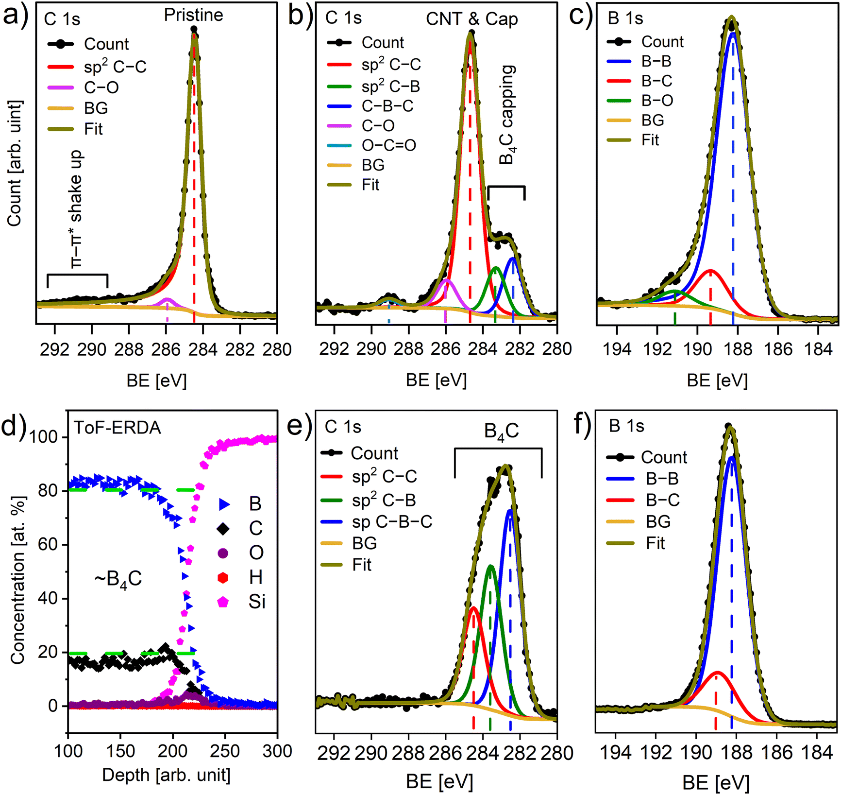 | ||
| Fig. 2 (a) C 1s core level spectra for the pristine CNT membrane, (b) C 1s and (c) B 1s core level spectra for the CNT membrane after CVD. For comparison, (d) show elemental composition from ToF-ERDA, (e) C 1s and (f) B 1s core level spectra obtained for a thicker a- B4C film deposited with the same CVD process on Si (100). | ||
Elemental composition from ToF-ERDA (Fig. 2d) of a thicker film on Si from the same CVD process gives 81 at% B, 18 at% C, 0.5 at% O and 0.2 at% H, i.e., a B4C stoichiometry of the film, corresponding to the low temperature phases of B13C2 or B12C3.33,49 XPS on this B4C reference film shows an agreement with the XPS spectra of the CNTs after CVD. The C 1s spectrum of the reference film (Fig. 2e) can be fitted with the same components corresponding to C–B and C–B–C bonds as the C 1s spectrum of the CNTs after CVD. The fitting curve corresponding to amorphous carbon in the reference film aligns with the higher intensity peak from the C–C bonds in the membrane. Presence of some amorphous carbon phase is typical in boron carbide CVD deposition from metalorganic precursors.46,50 The B 1s XPS spectrum of the reference film (Fig. 2f) show a similar B–B to B–C signal intensity ratio as in the B 1s spectrum of the CNTs after CVD. In addition, the C–B to C–B–C intensity ratio is similar in the CNTs after CVD and in the reference film, suggesting that the process rendered a similar material deposition on Si and the CNT membrane.
These observations and the preservation of the strong C–C bonds and the emergence of an additional shoulder peak, characteristic of the B4C film, suggest that the CVD process does not cause any chemical decomposition of the nanotube structure.
We further studied the compatibility of the B4C deposition by Raman spectroscopy before and after the CVD process, as the deposition may induce strain or defects in the CNT structure that will influence the vibrational modes,51,52 see Fig. 3. The Raman spectra of CNTs typically exhibit three main features, the radial breathing mode (RBM), the G band, and the D band. The G band is a vibration mode that involves the stretching of the C–C bonds along the CNT axis, see Fig. 3a.52,53 The G band frequency reflects the bond length and angle of the carbon atoms, and thus the strain and stress in the CNT. The D band intensity reflects defects and doping in CNTs, with the D peak being activated by the breathing vibrational mode of hexagonal rings necessitating a defect.54 The RBM is a vibration mode in which all the carbon atoms move radially in and out, like a breathing motion (Fig. 3a).55 The RBM frequency depends on the diameter, chirality, and structure of the CNT, as well as the external factors, such as strain, pressure, and temperature. It can be noted from Fig. 3b that the CVD process slightly shifted the G band peak position. G band peak center observed at 1572.4 cm−1 for the pristine CNT membrane red-shifted to 1568.9 cm−1 after the CVD process. We attribute this to the reflection of the average stress experienced by the CNT surfaces due to the film deposition.56 The G band to D band intensity ratio (IG/ID) which is commonly used for screening the quality of the CNTs changed from 43 to 23.5 showing that the CVD process induced modification in the CNT surface.57,58 Nevertheless, the vibrational mode analysis has several limitations despite its quick and convenient nature.59 The diverse attributes contributing to the vibrational band make the quantitative analysis difficult. The membrane structure, consisting of randomly oriented nanotubes with various diameters, further complicates the analysis. Despite this complexity, we suggest that the CVD process, while modifying the exterior walls as expected and needed for the film growth, exhibits good compatibility with the CNTs. This is evidenced by the preservation of structural integrity, indicated by higher G-band and lower D-band band intensities, as well as RBM. Furthermore, the intense peak from the sp2 hybridized C–C bonds and the extra shoulder peak corresponding to the film contributions observed from the XPS measurement align with this observation.
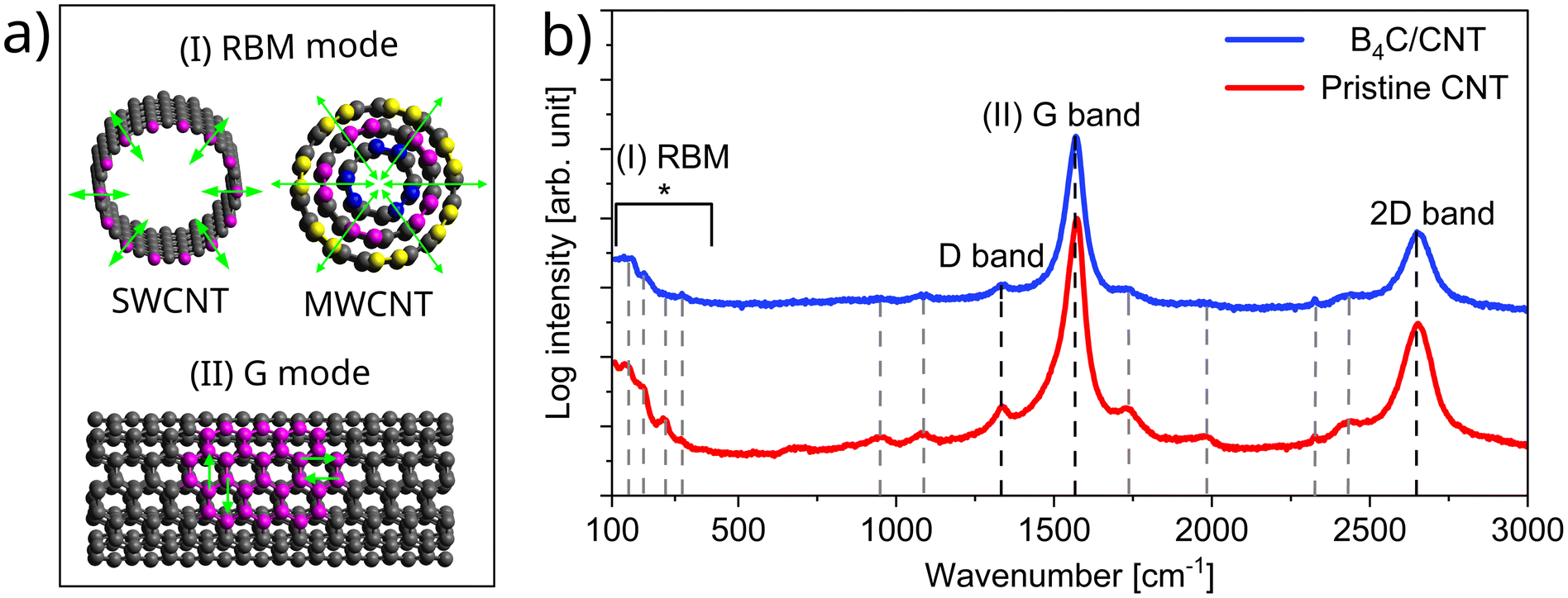 | ||
| Fig. 3 (a) Schematics illustrating G and RBM vibrational modes of CNTs, and (b) Raman spectra obtained for the pristine CNT membrane and the CNT membrane after the CVD process with an added Y-axis offset. | ||
We did not observe any Raman signal from the deposited B4C, which can be explained by the high intensity of the Raman signals from the CNTs hiding lower intensity signals from B4C. The amorphous nature of the B4C can also contribute to the loss of signal intensity. We therefore deposited a thicker B4C film on a Si wafer under the same conditions. While XRD measurement of the thicker B4C reference film on Si(100) suggests that the films are X-ray amorphous, Raman spectroscopy of the reference film indicates the presence of short-range order, as shown in Fig. 4. The broad peaks between 400–700 cm−1 and 800 to 1300 cm−1 are characteristic of an amorphous B4C phase with significant short range order.60 The fitted peak positions in the background deconvoluted curve align closely with reported values. While the peak centered at 325 cm−1 is associated with disorder activated vibrational modes,33 473 cm−1, 657 cm−1 and 831 cm−1, 933 cm−1 and 1090 cm−1 are closer to the reported values for B4C.61–63 The prominent peak observed at 473 cm−1 is indicative of the vibrational modes resulting from atomic displacements within the icosahedra structure.63 The minor peak at 1526 cm−1, is assigned as the G-band of amorphous carbon, indicating the presence of some amount of amorphous carbon. The C 1s core level XPS spectra (Fig. 2b) which show sp2 hybridized C–C, C bonded to sp hybridized B in the C–B–C chain, and sp2 hybridized C bonded to the equatorial B atoms in the icosahedra, consistent with Raman attributes. The Raman together with XPS suggest that the material has a disordered short-range order of B4C.
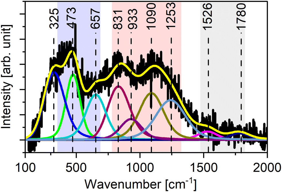 | ||
| Fig. 4 Raman spectroscopy measurement obtained for a thick B4C film deposited on a Si wafer. The spectrum was accrued by exciting with a 532 nm wavelength laser. The background deconvoluted spectra was fitted for the vibrational modes of the material. | ||
XRD analysis of the CNT membranes before and after the CVD process reveals a peak that corresponds to the 002-crystal plane of the CNTs (Fig. 5).6,64 Interestingly, the FWHM for the 002-peak reduced from 6.2 to 5.7 degrees after the deposition, indicating an increase in the average diameter of the nanotubes in the composite form.65 Since intratube and intertube contributions cause peak broadening, the standard Scherrer equation is not suitable for estimating tube diameter without resolving these components through curve fitting.64 While Raman spectroscopy (Fig. 3), shows a decrease in the IG/ID ratio, indicating surface modification after deposition, XRD analysis suggests that the CVD process did not modify the CNTs lattice. Instead, it apparently shows an increase in the average diameter in composite form, indicating a possible lattice matched interface.
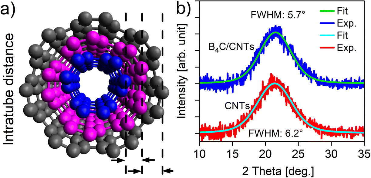 | ||
| Fig. 5 (a) schematic illustration showing intratubular distance that scatters coherently giving rise to the 002-peak position, and (b) the background-subtracted XRD curve corresponding to the 002-peaks, with Gaussian fit, showing respective FWHM. | ||
From the characterization above, we conclude that the B4C film grows on the CNTs without destroying their structure. B4C is built up of B icosahedra and is known for its octet rule violation meaning that it does not have enough valence electrons to form the standard two-electron two-center bond within the icosahedra, resulting in more than two atoms sharing a pair of electrons.45,48 We speculate that the electron deficient boron icosahedra interacts with the out-of-plane π-cloud of the rolled-up graphene-like structure of the CNTs. Electron diffraction measurement presented in Fig. 6 shows a broad frequency band centered around the theoretical 2–21 and 4–32 reflections of B4C R-3m, confirming short range order. Interestingly, the 1–14 CNT reflection overlaps with the 4–32 B4C reflection at a 0.3% mismatch, a prerequisite for epitaxy. The observed reduction in the FWHM of the 002-plane peak (Fig. 5), suggesting an apparent increase in average diameter, is consistent with the observation of near surface lattice matching, which allows some more X-rays to scatter coherently and resembles an increase in the average number of walls in the distribution.
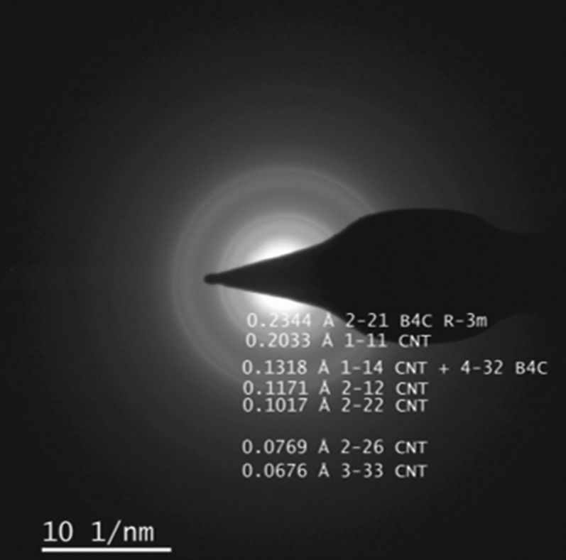 | ||
| Fig. 6 Electron diffraction pattern obtained for the B4C deposited carbon nanotube membrane. | ||
The ability to control the film thickness during the CVD process provides pore size tunability. Pore dimension and transmittance properties of CNT membranes critically determine their efficiency in molecular and ionic transport and separation.66 These parameters can influence the permeation and molecular discrimination capabilities of the CNT membrane. From Fig. 7, it can be observed that the pore size of CNT membrane can be tuned by depositing conformal B4C thin films of desired thickness. We note that the 3, 5 and 8 nm thick films, deposited for 90, 120, and 150 s, respectively, reduced the porosity of the membrane from 0.70 to 0.65, 0.60, and 0.52, respectively. This is important for various applications where specific pore sizes are desired.1,67,68 In addition to the inherent tunability of pristine CNT membrane, our conformal B4C deposition process allows a second stage of porosity control. This process allows precise adjustment of membrane thickness, enabling fine-tuning of pore size.
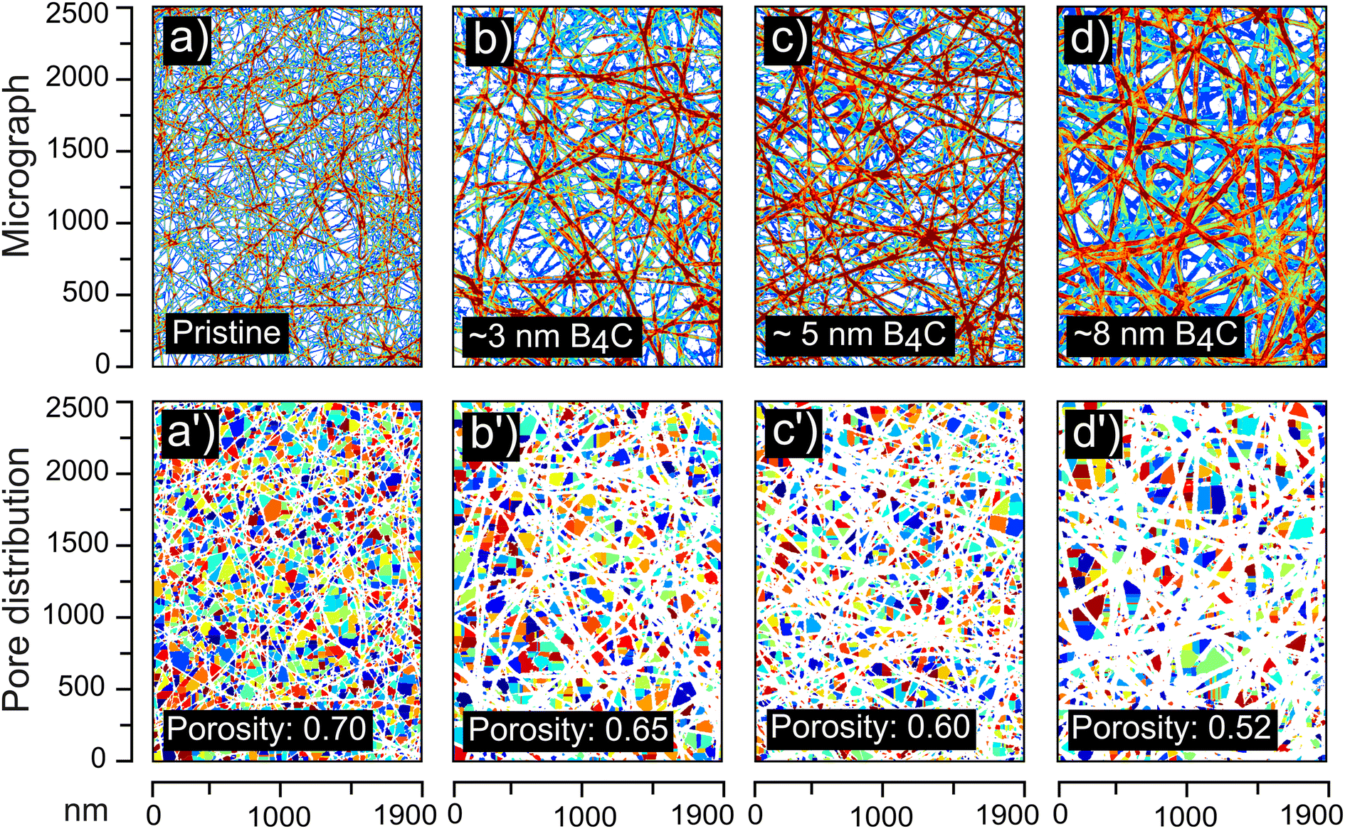 | ||
| Fig. 7 Image processed SEM micrographs and pore segmentation map obtained for the (a) pristine CNT membrane, and (b)–(d) B4C deposited CNT membrane with a film thickness of (b) 3 nm (c) 5 nm and (d) 8 nm. (a′)–(d′) shows respective pore segmentation map showing that porosity changed from 0.70 to 0.52. See ESI† for details on the image processing. | ||
It can also be noted from these experiments that the film thickness as a function of deposition time does not intersect origin. This can be interpreted as a nucleation delay in the deposition process. Such a delay is not unexpected and found in several CVD processes.
4. Conclusions
Our study demonstrated deposition of fully uniform amorphous boron carbide (B4C) thin films on carbon nanotubes (CNTs) by a conformal CVD process. No clustering or clogging at the pore sites are seen from STEM and SEM analysis. XPS, Raman spectroscopy and Electron diffraction measurement collectively show that the deposition of B4C films does not cause any structural modification to the CNT lattice, and it remains intact. The observed near-surface lattice matched interface and the amorphous growth towards the exterior prevent the introduction of residual stress during the film deposition. Image processing techniques affirmed the compatibility of the deposition process with the ability to precisely control the thickness, highlighting the tunability of pore sizes in the B4C deposition process. This conformal deposition process of B4C on CNTs within a membrane structure provides new possibilities to modify the properties of CNT membranes.Data availability
The data that support the findings of this study are available from the corresponding author upon a reasonable request.Conflicts of interest
We have no conflict of interests to declare.Acknowledgements
The assistance of Pentti Niiranen for the XPS measurement is gratefully acknowledged. Canatu Oy is gratefully acknowledged for providing the Carbon nanotube membranes. Financial support by the Swedish Research Council (VR) under Contract No. 2018-05499, from the Swedish Government Strategic Research Area in Materials Science on Advanced Functional Materials at Linköping University (Faculty Grant SFO-Mat-LiU No. 2009-00971), and from the Swedish Research Council VR-RFI (No. 2019-00191) for the Accelerator based ion-technological centre in Uppsala, are gratefully acknowledged. Access to ARTEMI, the Swedish National Infrastructure in Advanced Electron Microscopy, via the Swedish Research Council and the Swedish Foundation for Strategic Research for (2021-00171 and RIF21-0026) is gratefully acknowledged.References
- M. Y. Timmermans, I. Pollentier, M. Korytov, T. Nuytten, S. Sergeant, T. Conard, J. Meersschaut, Y. Zhang, M. Dialameh, W. Alaerts, E. Jazaeri, V. Spampinato, A. Franquet, S. Brems, C. Huyghebaert and E. E. Gallagher, CNT EUV pellicle tunability and performance in a scanner-like environment, in Extrem. Ultrav. Lithogr. XII, SPIE, ed. N. M. Felix and A. Lio, 2021, pp. 34. DOI:10.1117/12.2584519.
- Y. Li, Carbon Nanotube Research in Its 30th Year, ACS Nano, 2021, 15, 9197–9200, DOI:10.1021/acsnano.1c04972.
- E. G. Rakov, Chemistry of Carbon Nanotubes, Carbon Nanomater., 2006, 77–147, DOI:10.1201/9781420009378-7.
- J. Barkauskas, pH-dependent water penetration through CNT sub-layers arranged on the polycarbonate membrane filters, Carbon, 2010, 48, 1858–1861, DOI:10.1016/j.carbon.2010.01.022.
- M. Y. Timmermans, I. Pollentier, J. U. Lee, J. Meersschaut, O. Richard, C. Adelmann, C. Huyghebaert and E. E. Gallagher, CNT EUV pellicle: moving towards a full-size solution, Proc. SPIE 10451, Photomask Technology 2017, 104510P, 2017, DOI:10.1117/12.2280632.
- Y. Liu, S. Zhang, J. Guo, W. Qiu, G. Zhou and Q. Li, Debundling and reorganization of CNT networks under high temperature treatment, Carbon, 2024, 222, 119004, DOI:10.1016/j.carbon.2024.119004.
- D. Yang, D. Tian, C. Xue, F. Gao, Y. Liu, H. Li, Y. Bao, J. Liang, Z. Zhao and J. Qiu, Tuned Fabrication of the Aligned and Opened CNT Membrane with Exceptionally High Permeability and Selectivity for Bioalcohol Recovery, Nano Lett., 2018, 18, 6150–6156, DOI:10.1021/acs.nanolett.8b01831.
- J. Saththasivam, W. Yiming, K. Wang, J. Jin and Z. Liu, A Novel Architecture for Carbon Nanotube Membranes towards Fast and Efficient Oil/water Separation, Sci. Rep., 2018, 8, 4–9, DOI:10.1038/s41598-018-25788-9.
- B. Lee, Y. Baek, M. Lee, D. H. Jeong, H. H. Lee, J. Yoon and Y. H. Kim, A carbon nanotube wall membrane for water treatment, Nat. Commun., 2015, 6, 7109, DOI:10.1038/ncomms8109.
- L. Sun, X. He and J. Lu, Super square carbon nanotube network: a new promising water desalination membrane, npj Comput. Mater., 2016, 2, 16004, DOI:10.1038/npjcompumats.2016.4.
- Q. Tu, Q. Yang, H. Wang and S. Li, Rotating carbon nanotube membrane filter for water desalination, Sci. Rep., 2016, 6, 26183, DOI:10.1038/srep26183.
- C. Xue, G.-Q. Du, L.-J. Chen, J.-G. Ren, J.-X. Sun, F.-W. Bai and S.-T. Yang, A carbon nanotube filled polydimethylsiloxane hybrid membrane for enhanced butanol recovery, Sci. Rep., 2014, 4, 5925, DOI:10.1038/srep05925.
- X. Cui, J. Chen, T. Wang and W. Chen, Rechargeable Batteries with High Energy Storage Activated by In situ Induced Fluorination of Carbon Nanotube Cathode, Sci. Rep., 2014, 4, 5310, DOI:10.1038/srep05310.
- J. U. Lee, J. Vanpaemel, I. Pollentier, C. Adelmann, H. Zahedmanesh, C. Huyghebaert, M. Timmermans, M. De Volder and E. Gallagher, Introducing the EUV CNT pellicle, in Photomask Technol, ed. B. S. Kasprowicz and P. D. Buck, 2016, pp. 99850C. DOI:10.1117/12.2243019.
- Ihsanullah, T. Laoui, A. M. Al-Amer, A. B. Khalil, A. Abbas, M. Khraisheh and M. A. Atieh, Novel anti-microbial membrane for desalination pretreatment: A silver nanoparticle-doped carbon nanotube membrane, Desalination, 2015, 376, 82–93, DOI:10.1016/j.desal.2015.08.017.
- I. Pollentier, M. Y. Timmermans, C. Huyghebaert, S. Brems and E. Gallagher, The EUV CNT pellicle: balancing material properties to optimize performance, 2020, pp. 47. DOI:10.1117/12.2552357.
- I. Pollentier, J. Vanpaemel, J. U. Lee, C. Adelmann, H. Zahedmanesh, C. Huyghebaert and E. E. Gallagher, EUV lithography imaging using novel pellicle membranes, in Extrem. Ultrav. Lithogr. VII, ed. E. M. Panning and K. A. Goldberg, 2016, pp. 977620. DOI:10.1117/12.2220031.
- V. Vatanpour, S. S. Madaeni, R. Moradian, S. Zinadini and B. Astinchap, Novel antibifouling nanofiltration polyethersulfone membrane fabricated from embedding TiO2 coated multiwalled carbon nanotubes, Sep. Purif. Technol., 2012, 90, 69–82, DOI:10.1016/j.seppur.2012.02.014.
- E. Shi, L. Zhang, Z. Li, P. Li, Y. Shang, Y. Jia, J. Wei, K. Wang, H. Zhu, D. Wu, S. Zhang and A. Cao, TiO2-Coated Carbon Nanotube-Silicon Solar Cells with Efficiency of 15%, Sci. Rep., 2012, 2, 884, DOI:10.1038/srep00884.
- K. Moulaee, M. H. Raza, N. Pinna, N. Donato and G. Neri, Effect of Al2O3 thickness on performance of Al2O3/CNTS in the electrochemical sensing of di- hydroxybenzene isomers, in 2019 IEEE SENSORS, IEEE, 2019, pp. 1–4. DOI:10.1109/SENSORS43011.2019.8956581.
- L. Huang, S. P. Lau, H. Y. Yang, E. S. P. Leong, S. F. Yu and S. Prawer, Stable superhydrophobic surface via carbon nanotubes coated with a ZnO thin film, J. Phys. Chem. B, 2005, 109, 7746–7748, DOI:10.1021/jp046549s.
- H. Zhou, L. Zhang, D. Zhang, S. Chen, P. R. Coxon, X. He, M. Coto, H.-K. Kim, K. Xi and S. Ding, A universal synthetic route to carbon nanotube/transition metal oxide nano-composites for lithium ion batteries and electrochemical capacitors, Sci. Rep., 2016, 6, 37752, DOI:10.1038/srep37752.
- A. Kongkanand and P. V. Kama, Electron Storage in Single Wall Carbon Semiconductor – SWCNT Suspensions, ACS Nano, 2007, 1, 13–21 CrossRef CAS PubMed.
- F. Rivadulla, C. Mateo-Mateo and M. A. Correa-Duarte, Layer-by-Layer Polymer Coating of Carbon Nanotubes: Tuning of Electrical Conductivity in Random Networks, J. Am. Chem. Soc., 2010, 132, 3751–3755, DOI:10.1021/ja910572b.
- N. G. Sahoo, Y. C. Jung, H. H. So and J. W. Cho, Polypyrrole coated carbon nanotubes: Synthesis, characterization, and enhanced electrical properties, Synth. Met., 2007, 157, 374–379, DOI:10.1016/j.synthmet.2007.04.006.
- S. S. Y. Law, G. Liou, Y. Nagai, J. Giménez-Dejoz, A. Tateishi, K. Tsuchiya, Y. Kodama, T. Fujigaya and K. Numata, Polymer-coated carbon nanotube hybrids with functional peptides for gene delivery into plant mitochondria, Nat. Commun., 2022, 13, 2417, DOI:10.1038/s41467-022-30185-y.
- A. L. Gorkina, A. P. Tsapenko, E. P. Gilshteyn, T. S. Koltsova, T. V. Larionova, A. Talyzin, A. S. Anisimov, I. V. Anoshkin, E. I. Kauppinen, O. V. Tolochko and A. G. Nasibulin, Transparent and conductive hybrid graphene/carbon nanotube films, Carbon, 2016, 100, 501–507, DOI:10.1016/j.carbon.2016.01.035.
- M. Varga, T. Izak, V. Vretenar, H. Kozak, J. Holovsky, A. Artemenko, M. Hulman, V. Skakalova, D. S. Lee and A. Kromka, Diamond/carbon nanotube composites: Raman, FTIR and XPS spectroscopic studies, Carbon, 2017, 111, 54–61, DOI:10.1016/j.carbon.2016.09.064.
- T. Umeyama, N. Tezuka, M. Fujita, S. Hayashi, N. Kadota, Y. Matano and H. Imahori, Clusterization, electrophoretic deposition, and photoelectrochemical properties of fullerene-functionalized carbon nanotube composites, Chem. – Eur. J., 2008, 14, 4875–4885, DOI:10.1002/chem.200702053.
- F. Yang, S. Ma, C. M. Khor, Y. Su, Z. Barani, Z. Xu, A. Boyko, A. Iddya, N. Segev-Mark, X. (Rayne) Zheng, F. Kargar, A. A. Balandin, G. Ramon, I. De Rosa, E. Hoek and D. Jassby, One-step method for the fabrication of pure and metal-decorated densified CNT films for effective electromagnetic interference shielding, Carbon, 2023, 214, 118370, DOI:10.1016/j.carbon.2023.118370.
- S. M. George, Atomic layer deposition: An overview, Chem. Rev., 2010, 110, 111–131, DOI:10.1021/cr900056b.
- V. Cremers, R. L. Puurunen and J. Dendooven, Conformality in atomic layer deposition: Current status overview of analysis and modelling, Appl. Phys. Rev., 2019, 6, 021302, DOI:10.1063/1.5060967.
- V. Domnich, S. Reynaud, R. A. Haber and M. Chhowalla, Boron carbide: Structure, properties, and stability under stress, J. Am. Ceram. Soc., 2011, 94, 3605–3628, DOI:10.1111/j.1551-2916.2011.04865.x.
- T. S. Kim, J. H. Yeo, K. B. Nam, M. J. Kim and J. B. Yoo, Boron carbide coating to improve the chemical stability of nm-thick graphite films, Thin Solid Films, 2020, 704, 138002, DOI:10.1016/j.tsf.2020.138002.
- P. G. Valentine, P. W. Trester, J. Winter, J. Linke, R. Duwe, E. Wallura and V. Philipps, Boron carbide based coatings on graphite for plasma-facing components, J. Nucl. Mater., 1994, 212–215, 1146–1152, DOI:10.1016/0022-3115(94)91011-1.
- A. H. Choolakkal, P. Niiranen, S. Dorri, J. Birch and H. Pedersen, Competitive co-diffusion as a route to enhanced step coverage in chemical vapor deposition, Nat. Commun., 2024, 15, 10667, DOI:10.1038/s41467-024-55007-1.
- J. Etula, A. Soliman, T. Ghosh, B. Mikladal, E. Salmi, E. Van Veldhoven, K. Chernenko, I. Varjos and T. Juntunen, Carbon nanotube membranes for EUV photolithography: a versatile material platform, in Int. Conf. Extrem. Ultrav. Lithogr. 2023, SPIE, ed. K. G. Ronse, P. A. Gargini, P. P. Naulleau and T. Itani, 2023, pp. 43. DOI:10.1117/12.2686790.
- J. Etula, B. Mikladal, M. Makkonen, E. Kauppinen and I. Varjos, Small scale, big impact: the world's thinnest and strongest free-standing carbon nanotube membrane, in Int. Conf. Extrem. Ultrav. Lithogr. 2021, SPIE, ed. K. G. Ronse, P. A. Gargini, E. Hendrickx, P. P. Naulleau and T. Itani, 2021, pp. 3. DOI:10.1117/12.2599072.
- N. Fairley, V. Fernandez, M. Richard-Plouet, C. Guillot-Deudon, J. Walton, E. Smith, D. Flahaut, M. Greiner, M. Biesinger, S. Tougaard, D. Morgan and J. Baltrusaitis, Systematic and collaborative approach to problem solving using X-ray photoelectron spectroscopy, Appl. Surf. Sci. Adv., 2021, 5, 100112, DOI:10.1016/j.apsadv.2021.100112.
- K. Arstila, J. Julin, M. I. Laitinen, J. Aalto, T. Konu, S. Kärkkäinen, S. Rahkonen, M. Raunio, J. Itkonen, J.-P. Santanen, T. Tuovinen and T. Sajavaara, Potku – New analysis software for heavy ion elastic recoil detection analysis, Nucl. Instrum. Methods Phys. Res., Sect. B, 2014, 331, 34–41, DOI:10.1016/j.nimb.2014.02.016.
- R. L. W. Smithson, D. J. McClure and D. F. Evans, Effects of polymer substrate surface energy on nucleation and growth of evaporated gold films, Thin Solid Films, 1997, 307, 110–112, DOI:10.1016/S0040-6090(97)00310-6.
- J. Su, C. B. Musgrave, Y. Song, L. Huang, Y. Liu, G. Li, Y. Xin, P. Xiong, M. M.-J. Li, H. Wu, M. Zhu, H. M. Chen, J. Zhang, H. Shen, B. Z. Tang, M. Robert, W. A. Goddard and R. Ye, Strain enhances the activity of molecular electrocatalysts via carbon nanotube supports, Nat. Catal., 2023, 6, 818–828, DOI:10.1038/s41929-023-01005-3.
- Y.-S. Li, J.-L. Liao, S.-Y. Wang and W.-H. Chiang, Intercalation-assisted longitudinal unzipping of carbon nanotubes for green and scalable synthesis of graphene nanoribbons, Sci. Rep., 2016, 6, 22755, DOI:10.1038/srep22755.
- M. Imam, L. Souqui, J. Herritsch, A. Stegmüller, C. Höglund, S. Schmidt, R. Hall-Wilton, H. Högberg, J. Birch, R. Tonner and H. Pedersen, Gas Phase Chemistry of Trimethylboron in Thermal Chemical Vapor Deposition, J. Phys. Chem. C, 2017, 121, 26465–26471, DOI:10.1021/acs.jpcc.7b09538.
- S. Mondal, E. Bykova, S. Dey, S. I. Ali, N. Dubrovinskaia, L. Dubrovinsky, G. Parakhonskiy and S. Van Smaalen, Disorder and defects are not intrinsic to boron carbide, Sci. Rep., 2016, 6, 11–16, DOI:10.1038/srep19330.
- M. Imam, C. Höglund, J. Jensen, S. Schmidt, I. G. Ivanov, R. Hall-Wilton, J. Birch and H. Pedersen, Trimethylboron as single-source precursor for boron-carbon thin film synthesis by plasma chemical vapor deposition, J. Phys. Chem. C, 2016, 120, 21990–21997, DOI:10.1021/acs.jpcc.6b06529.
- K. Rasim, R. Ramlau, A. Leithe-Jasper, T. Mori, U. Burkhardt, H. Borrmann, W. Schnelle, C. Carbogno, M. Scheffler and Y. Grin, Local Atomic Arrangements and Band Structure of Boron Carbide, Angew. Chem., Int. Ed., 2018, 57, 6130–6135, DOI:10.1002/anie.201800804.
- M. M. Balakrishnarajan, P. D. Pancharatna and R. Hoffmann, Structure and bonding in boron carbide: The invincibility of imperfections, New J, Chem, 2007, 31, 473, 10.1039/b618493f.
- A. Jay, O. Hardouin Duparc, J. Sjakste and N. Vast, Theoretical phase diagram of boron carbide from ambient to high pressure and temperature, J. Appl. Phys., 2019, 125, 185902, DOI:10.1063/1.5091000.
- M. Imam, C. Höglund, S. Schmidt, R. Hall-Wilton, J. Birch and H. Pedersen, Plasma CVD of hydrogenated boron-carbon thin films from triethylboron, J. Chem. Phys., 2018, 148, 034701, DOI:10.1063/1.5006886.
- K. P. S. S. Hembram, J. G. Kim, S. G. Lee, J. Park and J. K. Lee, Radial-tangential mode of single-wall carbon nanotubes manifested by Landau regulation: reinterpretation of low- and intermediate-frequency Raman signals, Sci. Rep., 2023, 13, 1–8, DOI:10.1038/s41598-023-32018-4.
- A. Jorio and R. Saito, Raman spectroscopy for carbon nanotube applications, J. Appl. Phys., 2021, 129, 021102, DOI:10.1063/5.0030809.
- M. S. Dresselhaus, G. Dresselhaus, R. Saito and A. Jorio, Raman spectroscopy of carbon nanotubes, Phys. Rep., 2005, 409, 47–99, DOI:10.1016/j.physrep.2004.10.006.
- A. C. Ferrari and D. M. Basko, Raman spectroscopy as a versatile tool for studying the properties of graphene, Nat. Nanotechnol., 2013, 8, 235–246, DOI:10.1038/nnano.2013.46.
- Z. Li, L. Deng, I. A. Kinloch and R. J. Young, Raman spectroscopy of carbon materials and their composites: Graphene, nanotubes and fibres, Prog. Mater. Sci., 2023, 135, 101089, DOI:10.1016/j.pmatsci.2023.101089.
- C. Hu, J. Chen, X. Zhou, Y. Xie, X. Huang, Z. Wu, S. Ma, Z. Zhang, K. Xu, N. Wan, Y. Zhang, Q. Liang and Z. Shi, Collapse of carbon nanotubes due to local high-pressure from van der Waals encapsulation, Nat. Commun., 2024, 15, 3486, DOI:10.1038/s41467-024-47903-3.
- H. Y. Yang, Z. J. Han, S. F. Yu, K. L. Pey, K. Ostrikov and R. Karnik, Carbon nanotube membranes with ultrahigh specific adsorption capacity for water desalination and purification, Nat. Commun., 2013, 4, 2220, DOI:10.1038/ncomms3220.
- M. Szybowicz, A. B. Nowicka and A. Dychalska, Characterization of carbon nanomaterials by raman spectroscopy, Elsevier Ltd., 2018. DOI:10.1016/B978-0-08-101973-3.00001-8.
- J. Hodkiewicz, Rapid Quality Screening of Carbon Nanotubes with Raman Spectroscopy, 2010, pp. 1–4 Search PubMed.
- C. Pallier, J.-M. Leyssale, L. A. Truflandier, A. T. Bui, P. Weisbecker, C. Gervais, H. E. Fischer, F. Sirotti, F. Teyssandier and G. Chollon, Structure of an Amorphous Boron Carbide Film: An Experimental and Computational Approach, Chem. Mater., 2013, 25, 2618–2629, DOI:10.1021/cm400847t.
- K. M. Reddy, P. Liu, A. Hirata, T. Fujita and M. W. Chen, Atomic structure of amorphous shear bands in boron carbide, Nat. Commun., 2013, 4, 2483, DOI:10.1038/ncomms3483.
- H. Werheit, T. Au, R. Schmechel, S. O. Shalamberidze, G. I. Kalandadze and A. M. Eristavi, IR-Active Phonons and, Structure Elements of Isotope-Enriched Boron Carbide, J. Solid State Chem., 2000, 154, 79–86, DOI:10.1006/jssc.2000.8815.
- R. Lazzari, N. Vast, J. M. Besson, S. Baroni and A. D. Corso, Atomic structure and vibrational properties of icosahedral b4c boron carbide, Phys. Rev. Lett., 1999, 83, 3230–3233, DOI:10.1103/PhysRevLett.83.3230.
- D. N. Futaba, T. Yamada, K. Kobashi, M. Yumura and K. Hata, Macroscopic wall number analysis of single-walled, double-walled, and few-walled carbon nanotubes by X-ray diffraction, J. Am. Chem. Soc., 2011, 133, 5716–5719, DOI:10.1021/ja2005994.
- C. F. Holder and R. E. Schaak, Tutorial on Powder X-ray Diffraction for Characterizing Nanoscale Materials, ACS Nano, 2019, 13, 7359–7365, DOI:10.1021/acsnano.9b05157.
- R. Smajda, Á. Kukovecz, Z. Kónya and I. Kiricsi, Structure and gas permeability of multi-wall carbon nanotube buckypapers, Carbon, 2007, 45, 1176–1184, DOI:10.1016/j.carbon.2007.02.022.
- J. Bekaert, E. Gallagher, R. Jonckheere, L. Van Look, R. Aubert, V. V. Nair, M. Y. Timmermans, I. Pollentier, E. Hendrickx, A. Klein, G. Yeǧen and P. Broman, Carbon nanotube pellicles: Imaging results of the first full-field extreme ultraviolet exposures, J. Micro/Nanopatterning, Mater., Metrol., 2021, 20, 1–10, DOI:10.1117/1.JMM.20.2.021005.
- M. Y. Timmermans, M. Mariano, I. Pollentier, O. Richard, C. Huyghebaert and E. E. Gallagher, Free-standing carbon nanotube films for extreme ultraviolet pellicle application, J. Micro/Nanolithogr., MEMS, MOEMS, 2018, 17, 1, DOI:10.1117/1.JMM.17.4.043504.
Footnote |
| † Electronic supplementary information (ESI) available: MATLAB scripts used for image processing and porosity estimation. See DOI: https://doi.org/10.1039/d4nr04704d |
| This journal is © The Royal Society of Chemistry 2025 |