
 Open Access Article
 This Open Access Article is licensed under a Creative Commons Attribution-Non Commercial 3.0 Unported Licence
Facile integration of single-crystalline phthalocyanine nanowires and nanotrees as photo-enhanced conductometric sensors†
A. Nicolás
Filippin
,
Ángel
Campos-Lendinez
,
Juan
Delgado-Alvarez
,
Gloria
Moreno-Martinez
,
Javier
Castillo-Seoane
,
Víctor J.
Rico
,
Vanda F.
Godinho
,
Ángel
Barranco
 ,
Juan R.
Sanchez-Valencia
* and
Ana
Borras
*
,
Juan R.
Sanchez-Valencia
* and
Ana
Borras
*
Nanotechnology on Surfaces and Plasma Lab, Materials Science Institute of Seville (CSIC-US), Americo Vespucio 49, 41092 Seville, Spain. E-mail: jrsanchez@icmse.csic.es; anaisabel.borras@icmse.csic.es
First published on 27th February 2025
Abstract
This article presents a reproducible and affordable methodology for fabricating organic nanowires (ONWs) and nanotrees (ONTs) as light-enhanced conductometric O2 sensors. This protocol is based on a solventless procedure for the formation of high-density arrays of nanowires and nanotrees on interdigitated electrodes. The synthesis combines physical vapour deposition for the self-assembled growth of free-phthalocyanine nanowires and soft plasma etching to prompt the nucleation sites on the as-grown ONWs to allow for the formation of nanotrees. Electrical conductivity in such low-dimensional electrodes was analysed in the context of density, length, and interconnection between nanowires and nanotrees. Furthermore, the electrodes were immersed in water to improve the nanowires’ connectivity. The response of the nanotrees as conductometric O2 sensors was tested at different temperatures (from room temperature to 100 °C), demonstrating that the higher surface area exposed by the nanotrees, in comparison with that of their polycrystalline thin film counterparts, effectively enhances the doping effect of oxygen and increases the response of the ONT-based sensor. Both organic nanowires and nanotrees were used as model systems to study the augmented response of the sensors provided by illumination with white or monochromatic light to organic semiconducting systems. Interestingly, the otherwise negligible sensor response at room temperature can be activated (On/Off) under LED illumination, and no dependency on the illumination wavelength in the visible range was observed. Thus, under low-power LED illumination with white light, we show a response to O2 of 16% and 37% in resistivity for organic nanotrees at room temperature and 100 °C, respectively. These results open the path to developing room temperature long-lasting gas sensors based on one- and three-dimensional single-crystalline small-molecule nanowires.
Introduction
The necessity for gas sensors operating at room temperature is a critical area of research, addressing the need for low-cost, low-power, portable, flexible and highly sensitive devices that could be integrated into modern electronic gadgets and wearables.1 Traditional metal–oxide semiconductor-based sensors suffer from high operating temperatures, limiting their practical use.2 The use of 2D materials such as graphene or MXenes for gas sensor applications has shown potential for flexible, room-temperature applications.3 Hybrid approaches combining graphene or MXenes with more sensitive sensing materials such as metal oxides4 or 2D transition metal dichalcogenides5 have shown potential to enhance sensitivity and selectivity.3In this context, organic-based sensors, including small molecules and polymers, offer the advantage of molecular design for achieving specificity to specific analytes.6–8 Moreover, the strong dependence of the physical properties of these organic building blocks on external conditions allows the fabrication of a wide range of sensors such as temperature, radiation, pressure, and chemical sensors, among others.7,9–13 These transducers can be used to monitor vital internal body parameters related to healthcare14–16 or external ones such as environmental agents (both hazardous and vital ones),7,8 opening the possibility for an entire sensing ecosystem. Among the different types of sensors, organic gas sensors have an attractive near future and more realistic possibility of their implementation in commercial devices. Some of the major drawbacks associated with the use of organic semiconductor molecules are their chemical degradation (stability) against some gaseous agents and long-term reliability issues.6,17–20 However, in contrast to their inorganic counterparts, organic molecules offer enormous structural flexibility and diversity through molecular engineering, which, along with improved device fabrication, offers the chance to overcome these problems. Moreover, they can exhibit considerably higher sensitivity and selectivity, lower operation temperature (even at room temperature operation), and shorter response and recovery time than commonly used metal oxides.21–23
Organic π-conjugated small molecules such as phthalocyanines have been one of the most studied families of organic semiconductors in gas sensing due to their tailorable chemical structures, mechanical flexibility, and good chemical and thermal stability.24–26 These molecules are processable under vacuum to produce high-quality amorphous or crystalline films on various substrates, further facilitating the fabrication of sensing devices. The conductivity of phthalocyanine films (the great majority being p-type semiconductors) at room temperature in air is relatively low, but when temperatures are raised above 100 °C, the conductivity increases significantly.27,28 The exposure of metal phthalocyanines (MPcs) to electrophilic gases such as NOx, Cl2, F2, BF3, or O2 produces an increase in the hole concentration in the film and a consequent increase in conductivity.29–31 On the other hand, reducing gases, such as NH3, tend to decrease the conductivity attributed to electron donation from the reducing gases to trap charge carriers.27,28 The interaction of analytes with the metal center in metallophthalocyanines (MPcs) modifies the material's charge distribution, altering its resistance and enabling gas detection.27–34 Furthermore, the metal center's electronic properties can be tailored to optimise the sensor's response to specific gases. For instance, zinc phthalocyanine (ZnPc) has shown potential in detecting complex analytes, including chemical warfare agents.35 The rational selection of the metal center, combined with the conjugated structure of phthalocyanines, contributes to the selective and sensitive detection of various gases.27–34
In the case of metal-free phthalocyanine (H2Pc), it is hypothesised that electrophilic species, including oxygen, are adsorbed on the molecules by weak interactions with the four meso-nitrogens or by hydrogen bonding to the two inner hydrogens, leading to a slight conductivity increase, although not as pronounced as in MPcs.27–34 The adsorption of analytes to phthalocyanines is considered to occur exclusively at the very surface of the films due to steric hindrance related to the tightness of the phthalocyanine crystal structure.27,36 In this sense, phthalocyanine nanowires (NWs) should provide a unique opportunity to enhance the sensing properties of these compounds owing to their larger surface area exposed to the analyte compared to that with the usual thin film approach.13,29,37 However, most studies on phthalocyanines as gas sensors are restricted to thin films or single-wire organic field effect transistor (OFET) operation.24,38–41 This latter approach, although with proven advantages such as high sensitivity and field-driven tunable selectivity, fails in a readily large-scale application since it relies on expensive and multistep procedures, including the synthesis of transductors, photo- or electron beam lithography and/or nano-handling of organic nanowires to build sensor devices.42–45
In such a context, we demonstrate herein a highly reproducible and affordable methodology for fabricating gas sensors consisting of high-density arrays of H2Pc single-crystalline organic nanowires (ONWs) synthesised by vacuum deposition on metallic electrodes. Our protocol has been exploited in the last few years for the growth of ONWs on processable and functional substrates such as metals (Au, Ag and Cu) and metal oxides (TiO2, ZnO, SiO2, FTO, and ITO) on silicon wafers, fused silica plates or polymeric supports (PDMS and PET).46–57 Thus, in contrast to most of the results in previous literature, where the transfer of 1D nanomaterials to different substrates to assemble sensors is usually required,29,42–45,58 here we present the direct fabrication of ONWs on Pt interdigitated substrates decorated with gold nanoparticles. It is important to outline that the sensor mechanism itself is not intrinsically dependent on the use of Pt or Au. In practical applications, cost-effective alternatives, such as other low-cost metals (Cu and Al), could replace these components without significantly compromising sensor performance. In addition, we explored different strategies to increase sensor sensitivity. We compared the single-crystal nanowire array sensor response to those of electrophilic (O2) and inert (Ar) gases with the performances of high surface-area organic nanotrees (ONTs) and highly interconnected wires processed by introducing an additional liquid evaporation route. Finally, organic nanowires and nanotrees serve as model systems to study the enhanced responses of the sensors provided by illumination with white or monochromatic light to organic semiconducting systems.
Experimental
Sensor fabrication
Commercial electrodes (Micrux) with 15 pairs of interdigitated Pt microelectrodes separated by 10 μm were used as received. Pt electrodes were chosen primarily due to their stability, reproducibility, and ready availability in our laboratory. While alternative, cost-effective metals such as Cu or Al could also be employed, Pt offers a significantly lower surface oxidation state, which is advantageous for research purposes. Before the sublimation of H2Pc, gold seeds were deposited to provide the necessary roughness for the growth of ONWs.46–49 The metallic seeds were deposited by magnetron sputtering under an Ar atmosphere at 0.1 mbar employing an Emitech K550 sputter coater equipped with a gold target of 60 mm diameter. The use of Au nanoparticles on Pt electrodes promotes the formation of discrete nanoparticles due to their favorable wetting characteristics, unlike the case of Au on Au substrates (for example, in case Au electrodes are chosen), which often result in thin films. To avoid conduction through the Au NPs, the deposition was performed at 12.5 mA for 10 seconds, ensuring the formation of isolated nanoparticles on the pre-patterned electrodes (see Fig. S1 in the ESI†). For the sublimation of H2Pc (29H,31H-phthalocyanine, Sigma-Aldrich, 98% purity), the base pressure was 10−6 mbar and the Ar pressure during deposition was set to 0.02 mbar. A Knudsen-type cell was used for sublimation (model LTE 01 supplied by Kurt J. Lesker) and the temperature was controlled to obtain a constant deposition rate of 0.5 Å s−1 measured using a quartz crystal monitor (QCM). The sample-to-evaporator distance was 6.5 cm and the substrate temperature was 170 °C. The nominal thickness of the primary ONWs was set to 3 kÅ (measured using QCM).For the growth of organic nanotrees,46–48,50 the primary ONWs were used as substrate and an oxygen plasma treatment of 20 minutes at 300 W was applied using a microwave plasma source ECR-SLAN operating at 2.45 GHz (Plasma Consult GmbH). The total oxygen pressure was 0.02 mbar, with the substrates at room temperature, and the sample-to-plasma distance set at 10 cm. The oxidative plasma treatment was followed by the growth of secondary ONWs under the same conditions as before but reducing the thickness to 1.5 kÅ (measured with the QCM). The as-grown ONWs were compared with highly interconnected nanowires obtained after solution post-treatment by immersion in water and subsequent drying. The final sensor was attached to the feedthrough, welding copper wires for electrical connections, and inserted into the measurement chamber (see ESI Scheme S1†).
Characterisation techniques
SEM micrographs were acquired using a Hitachi S4800 working at 2 kV on samples prepared on Si (100) substrates. Cross-sectional views were obtained by cleaving the substrates. The ONWs and ONTs were dispersed onto holey carbon films on Cu grids from Agar scientific for TEM characterization. High-resolution TEM was conducted using an FEI Tecnai Osiris TEM/STEM 80–200 operating at 200 kV. Raman spectra were recorded using a Horiba Jobin–Yvon LabRAM spectrometer equipped with a confocal microscope with a 50× objective and a laser of 532 nm wavelength with a spectral resolution of ∼1.7 cm−1. Low laser powers were utilised to prevent H2Pc damage. XPS characterisation was performed using a Phoibos 100 DLD X-ray spectrometer from SPECS. The spectra were collected in pass energy constant mode at 50 eV using an Mg Kα source. The C 1s signal at 284.8 eV was utilised to calibrate the binding energy in the spectra. The assignment of the BE to the different elements in the spectra corresponds to the data in ref. 59 and 60.Sensor characterisation
The electrical characterisation of the sensors and their response evaluation were performed using a Keithley 2635A system source meter working in sweep voltage mode for I–V curves and temporal evolution at a fixed potential of 5 V for the sensor response. The sensor was housed in a small, heatable chamber with an approximate volume of 50 cm3. Gases were introduced into the chamber using two calibrated mass-flow controllers (Bronkhorst), each set to deliver argon (99.99%) and oxygen (99.99%). Argon (Ar) was selected over other inexpensive inert gases, such as nitrogen, due to its higher chemical inertness, minimizing potential interference and ensuring that observed signal variations originate from the analyte (O2) rather than the carrier gas. Both Ar and O2 were supplied at a flow rate of 100 sccm, facilitating rapid atmospheric transitions within the chamber. A needle valve with a minimal aperture was installed at the outlet to prevent gas backflow. The chamber features a fused silica window, allowing for light illumination experiments. Heating of the chamber was achieved using an electrical resistance, with temperature monitored using a K-type thermocouple. Two different light sources were used, one a high-intensity Xe lamp (LASING ASB-Xe-175) and the other a multi-LED source (DiCon, Microscope Illuminator, MSB-MX-25) equipped with 3 LEDS (blue, green and red). The light power density was measured with a radiometer (Solarlight PMA21) at 5 cm from the samples at two different spectral ranges: UVA + UVB (detector PMA2107) and Vis + NIR (PMA2140).The relative response (R) of the sensor was calculated using the following relationship:61
Results and discussion
In this article, we have taken advantage of a previously reported vacuum deposition procedure for fabricating high-density arrays of supported organic nanowires.46–57 This high throughput method yields the growth of single-crystalline nanowires by self-assembly of planar and non-planar small molecules with high purity, growth rates, and homogeneity. A scheme for the growth of the ONWs is shown in Scheme S1 in the ESI†. In ref. 4 and 6–57, the growth of perylene-, metal and free phthalocyanine- and porphyrin-NWs supported on metal, metal oxide, polymeric and organic surfaces has been demonstrated and optimised. The growth mechanism of the ONWs responds to a combination of the single-crystalline structure formation promoted by the uniaxial anisotropy of molecular self-assembly by pi-stacking.46,47Thus, Fig. 1(a–c) show typical SEM images of the metal-free phthalocyanine (H2Pc) NWs formed on a Si(100) wafer decorated with Au nanoparticles. Lengths and widths of the ONWs are between 2–10 μm and 20–100 nm, respectively. As detailed in previous works,46,47,62 the growth of ONWs requires the presence of nucleation sites that can be added to the electrodes in the form of nanoparticles or thin films with a certain roughness. In this work, these required nucleation sites have been added as gold nanoparticles (NPs), ensuring no coalescence between them and, therefore, no electrical contact. A representative SEM image of the Au NP distribution is shown in Fig. S1.†
 | ||
| Fig. 1 SEM micrographs of the H2Pc ONWs deposited on a silicon wafer decorated with gold nanoparticles with planar views in panels (a and b) and cross-section in panel (c). SEM micrographs in a planar view (d) and cross-section (e and f) of the H2Pc ONTs. (g–i) Characteristic SEM micrographs of the supported ONWs after immersion in distilled water. | ||
The present approach aims to connect two preformed electrodes through the ONWs. Since the electrical connection is produced by the physical contact of two isolated wires growing from each electrode and aiming to increase the surface area, a highly branched organic nanotree architecture was used (Fig. 1(d–f)). A detailed report on the fabrication of such three-dimensional nanostructures can be found in ref. 4, 8 and 50. The procedure consists of using the primary ONWs as supports (i.e., acting as trunks) to form secondary ONWs (playing the role of branches). A soft-plasma etching treatment was carried out on the as-grown (primary) nanowires to generate a certain roughness that serves as the nucleation site for the formation of secondary wires. Thus, as shown in Fig. 1(d–f), the density of the ONWs is increased by more than an order of magnitude. Moreover, the lateral connectivity of the ONW layer is also improved through multiple contacts between the primary, secondary, and adjacent secondary ONWs. It is important to stress that the nanowires are single crystalline for both configurations, 1D and 3D. Fig. 2(a) and (b) show the high-resolution TEM image of an H2Pc nanowire (a) and the interconnection between primary and secondary nanowires forming a nanotree (b). The ONWs present the characteristic stripped pattern of the single-crystalline configuration corresponding to the self-assembly π-stacking growth mechanism along the nanowire length. The crystallinity is also evident from the digital diffraction pattern (DDP) at the right of the figure for the indicated area, where both the primary and the secondary ONWs present two maxima corresponding to the periodicity of the row of molecules visible in the TEM images. It is worth mentioning that the FFT image of the secondary wire presents four maxima, which are due to a change in the crystalline orientation at the vicinity of the branch (see the green circle in Fig. 2b), likely due to the presence of a dislocation. In the case of the connected ONWs, the plasma etching process to generate the nucleation centres for the formation of secondary branches was mild enough to keep a low roughness of the surface of the primary nanowire but likely produced an amorphous shell along the ONWs. Please note that the thickness of such an amorphous shell is extremely difficult to characterise as the ONW crystalline structure gets easily destroyed under the electron beam.46–48,54,63
 | ||
| Fig. 2 High-resolution transmission electron micrographs corresponding to an H2Pc nanowire (a) and the connected primary and secondary wires in an H2Pc nanotree (b). Digital diffraction patterns (DDPs) of the selected areas (right side of the figure) revealing the crystalline character of the ONWs and ONTs. | ||
Raman spectroscopy and X-ray photoelectron spectroscopy (XPS) were employed to validate the structural and elemental composition of the phthalocyanine nanostructures, which are shown in ESI S2 and S3,† respectively. Both techniques reveal that the ONWs present high purity from both the structural (from Raman) and chemical (from XPS) points of view. Further insights provided by XPS have also been included in ESI S3.†
It is worth stressing that the growth methodology of the ONWs and ONTs involves only dry vacuum steps of deposition and processing. In this article, and for the sake of comparison with other results in the literature, we have included an additional post-processing step, the immersion of the nanotrees in a solvent, in this case, distilled water (and subsequent drying), to further enhance the lateral connectivity. As shown in Fig. 1(g–i), water immersion significantly increases the number of interconnections between the ONWs. This is particularly clear in the cross-section image (i), where all the ONWs lying down close to the surface of the substrate can be observed.
Fig. 3(a) and (b) show SEM images of the commercial Pt interdigitated electrodes used for sensor fabrication at different magnifications. A brighter appearance of the metal can be noted, where the fingers of the interdigitated electrode are separated by 10 μm. Fig. 3(c) shows the ONTs grown onto the preformed electrodes (as detailed in Scheme S1 in the ESI†), where the high density of 1D nanostructures and the connectivity achieved can be observed. The metallic electrodes are partially visible behind the ONTs and can be noted with a different contrast in the SEM image of Fig. 3(c). Our methodology enables the direct growth of ONWs and ONTs onto the preformed electrodes at temperatures below 200 °C, eliminating the need for transfer steps and enhancing key factors such as electrical contact and reproducibility. Unlike most existing studies, which require higher temperatures, post-synthesis assembly or templated substrates,13,29,42–45,58 our approach achieves superior nanowire density and connectivity. While some prior works have demonstrated direct deposition on the preformed devices, the resulting nanowire networks exhibit significantly lower density and interconnectivity.37,64 In contrast, our method integrates a highly connected ONW network onto interdigitated electrodes. Additionally, the unique architecture of the branched ONTs, combined with an immersion-based strategy, further improves electrode bridging and enhances conductive pathways.
 | ||
| Fig. 3 SEM images of the commercial interdigitated electrodes before (a and b) and after (c) the deposition of H2PC nanotrees. I–V curves for the ONWs (d) and ONTs (e) on commercial electrodes at room temperature (black) and 100 °C (red) under a constant argon flux at ambient pressure. In addition, the I–V response of the device is shown after the water immersion treatment and subsequent drying. These curves were recorded at 100 °C under an Ar flux (blue curves). | ||
Fig. 3(d) and (e) present the I–V characteristics of the ONWs (d) and ONTs (e) at RT (black curve) and 100 °C (red curve). The I–V characteristics are nearly linear in all cases, indicating fair electrical contact between the nanowires and between the nanowires and the electrodes. This effect may have two different origins: (i) one is the match between the highest occupied molecular orbital (HOMO) of H2Pc and the work function of gold nanoparticles (used as nucleation centres to grow the ONWs), which are 5.7 eV65 and 5.5 eV,66 respectively and (ii) the second is the excellent interface in terms of cleanliness (the ONWs or ONTs are entangled while growing under vacuum) that ensures excellent contact between the wires.
The samples are highly resistive at room temperature, as shown in the I–V curves of Fig. 3(d) and (e) (note that the measurements have been performed under an Ar flux). The current flowing through the ONWs barely reaches 10−10 amperes at 5 volts, yielding a high resistance of 18.7 and 57.6 GΩ for the ONWs and ONTs, respectively. Such a high resistance can be understood due to the high intrinsic resistivity of the H2Pc molecule and due to the low cross-section of the ONWs, though, to the best of our knowledge, the resistivity of the ONWs of H2Pc has not yet been reported. ESI S4† provides an estimation of the number of contacts between the ONWs in adjacent electrode fingers to contextualise our results within the current literature.
It is noticeable that the measured resistance for the ONTs is higher than that for the ONWs. The nanowires and nanotrees were prepared under the same experimental conditions, since the ONWs are used as the initial trunk for the ONTs, and the only difference is an additional plasma treatment and subsequent deposition of the branches. Thus, the number of possible contacts between the trunks or the branches of the ONTs needs to be higher than that for the ONWs. Thus, the higher resistance value can be understood as an increase in the contact resistance between the nanotrees or by a deterioration of the conductivity of the initial trunk, surely related to the amorphisation of the primary ONW outer shell discussed in Fig. 2, both effects arising from the plasma treatment. This is also consistent with the Raman spectrum of the ONTs in Fig. S2† that shows a noisier spectrum, ascribed to surface amorphisation induced by the soft plasma treatment.
Although the oxygen treatment and subsequent growth of secondary branches in the ONTs may appear to be a stochastic process, the ONT-based sensors synthesized in this study exhibit a similar resistance. The resistance values measured under similar conditions (RT and Ar atmosphere) for three different ONT-based sensors synthesized in different batches are included in Table S1 in the ESI.† This suggests a level of reproducibility in their electrical properties, despite the seemingly random nature of structural modifications induced by the treatment.
In contrast, the resistance of the ONWs drops significantly with temperature, decreasing from 18.7 and 57.6 GΩ to 0.99 and 0.59 GΩ for the ONWs and ONTs, respectively. It is worth mentioning that this change in the resistance induced by the temperature is a reversible phenomenon, as can be observed in Fig. S5.† The resistivity of a semiconductor ONW or ONT is anticipated to decrease with temperature due to the electronic population of the lowest unoccupied molecular orbital (LUMO) levels. However, the observed reduction is much higher than the expected decrease in resistivity, which has been reported to decrease to half for H2Pc thin films (from ca. 2 to 1 × 10⁶ Ωm).28 The decrease in the resistance from RT to 100 °C for the ONW devices is about 15 times, while for the ONTs, this decrease is significantly enhanced, reducing their resistance by almost two orders of magnitude at 100 °C. These results are consistent with an overall decrease in the contact resistance between the wires induced by the temperature and would indicate that the number of contacts is higher in the case of the nanotrees (as expected) since the final resistance is lower for the ONTs at 100 °C. Following this reasoning and considering the higher number of contacts in the nanotree-based device, we immersed the samples in water to increase the contacts between the ONWs (or the ONTs), as shown in Fig. 1(g–i). As expected, the resistance can be further decreased for the ONWs from 0.99 to 0.64 GΩ and more for the ONTs from 0.59 to 0.16 GΩ. Even though the resistance values might seem high, it must be kept in mind that the conduction is achieved through a hopping mechanism between the NWs. Thus, the device's resistance can be decreased by shortening the distance between adjacent electrodes and/or increasing the hyperbranching. Due to the lower resistance of the most branched structures, all the sensors studied will be based on nanotrees.
As previously reported, the optoelectronic properties of phthalocyanine are modified when exposed to oxygen or oxidising gases present in the surroundings.24,40,67,68 However, the oxygen response is usually very slow for phthalocyanine-based sensors at room temperature, requiring their operation at elevated temperatures.24,40,67,68 In line with the literature, the RT response of the ONWs or ONTs to the change in the gas atmosphere from argon to oxygen is barely noticeable. The response is shown in Fig. 4(a) and magnified in Fig. 4(b) (black lines), which show the changes in the I–V curves after 10 minutes of pure oxygen and argon flow, with a minimal change in the resistance (from 19.9 to 23.3 GΩ, respectively). In contrast, Fig. 4(a) shows how the response at 100 °C is significantly enhanced, producing a decrease in the resistance from 1.0 to 0.49 GΩ for argon and oxygen environments, respectively. It is worth highlighting that the I–V curves were recorded after 10 minutes of oxygen or argon flow since prolonged times (especially under a pure oxygen atmosphere) produced a significantly higher decrease in the resistance of the devices. This effect can be seen in Fig. 4(c and d), where the initial resistance decrease is due to a 1-hour exposure to a pure oxygen atmosphere. Fig. 4(c) and (d) show the resistance of the device when the gas atmosphere is changed from pure Ar to O2 at 100 °C (c) and RT (d), respectively, at intervals of 5 minutes, imposing in all cases a bias of 5 V to the sensors. While switching the gas flux into the chamber from Ar to O2 at RT only produces a slight modification of the resistance of the device (Fig. 4d), the variation at 100 °C is significantly enhanced (Fig. 4c). Although the response of H2Pc thin films to oxygen increases at high temperatures—a well-known behaviour of this organic semiconductor— at 100 °C, this increase remains very small, as reported by other authors.67,69 In contrast, this study demonstrates a marked resistance response of the H2Pc ONTs to oxygen at 100 °C. The reported low response is usually attributed to the slow diffusion of oxygen in a thin film, since it is expected to be much slower than that in our branched structure. Thus, the much higher surface area exposed by the nanotrees effectively enhances the doping effect of oxygen and increases the response of the ONT-based sensor.
 | ||
| Fig. 4 (a) I–V curves for the ONTs deposited on commercial interdigitated electrodes at room temperature (black) and 100 °C (red) under a constant oxygen (solid line) or argon flux (dashed line) at ambient pressure. (b) Zoomed I–V curves in the highlighted area in (a) revealing the lack of response at room temperature. The curves have been recorded after 10 minutes of argon or oxygen flux. Resistance variation vs. time for the ONTs grown onto interdigitated electrodes at 100° (c) and RT (d). The system was dosed with pure oxygen for 1 hour and cyclically exposed to argon and oxygen for 5 minutes. | ||
The responses of the ONT-based sensors to oxygen/argon cycles were evaluated at different working temperatures and under combined irradiation. The response of the sensor upon illumination with a xenon lamp is shown in Fig. 5 at RT (a), 50 °C (b), and 100 °C (c) with red curves (labelled as UV + Vis). To discern the effect of the UV portion of the Xe lamp, a long-pass filter with a cut-on wavelength of 400 nm was used to illuminate the sensor (blue curves in Fig. 5, labelled as visible). As mentioned in Fig. (4d), for the room temperature case (Fig. 5a and c show the same curves as Fig. 4d and c, respectively, for comparison with the illuminated cases), by alternating between oxygen and argon flows, a very subtle saw-like resistance response was obtained that is masked by the noticeable drift in the curve. Upon visible light irradiation, the resistance decreases by three orders of magnitude and an enhanced sensor response can be noted due to light activation. This light activation arises due to the electronic population of the LUMO levels (as it occurs with temperature) inherent to the semiconductor nature of the molecules for light energies above the H2Pc band gap of 1.88 eV.70 On the other hand, UV + visible light does not produce any further resistance change compared to irradiation in the visible range. This behaviour is likely due to the tiny difference in the power density of visible and UV + visible radiation, which is roughly 73 mW cm−2 (Table S2 in the ESI†). Note that near-infrared radiation (NIR) was not eliminated from the light source; however, it should not affect the measurements due to the higher band gap of H2Pc. In addition, it was corroborated that NIR radiation did not produce any significant change in temperature during measurements, as evidenced by the thermocouple.
 | ||
| Fig. 5 Organic nanotree sensor response to oxygen and argon at RT (a), 50 °C (b), and 100 °C (c) without irradiation (black line), under visible light irradiation (blue), and under UV + visible light irradiation (red). | ||
Raising the temperature to 50 °C (Fig. 5b) and 100 °C (Fig. 5c) further decreases the resistance of the non-illuminated sensors by more than two orders of magnitude when comparing the 100 °C to the RT case. Besides, the drift observed in the RT case for the non-illuminated sensors decreased at 50 °C and is no longer present at 100 °C. Moreover, the sensor response reveals that the saw-like features of the curves were much more defined as the temperature increased, demonstrating again the role of temperature in the sensor performance. In contrast, the illumination of the sensors at 50 °C (Fig. 5b) and 100 °C (Fig. 5c), both with and without the UV component, results in a decrease in the resistance similar to the one encountered for the RT case. It is worth highlighting that the three graphs (Fig. 5a–c) present the same resistance range in the illuminated region (before the break of the graph), facilitating the comparison between the different temperature cases. These results indicate that the illumination effect on the conductivity is more pronounced than the increase in the temperature up to 100 °C. This is due to the high power of the lamp used, which has a total power of 1.77 W cm−2 (Table S2†). For the sake of comparison, Fig. S6† shows the sensor response to oxygen and argon for the three temperatures employed in Fig. 5 in the dark and under illumination. The resistance is graphed on a logarithmic scale and is the same for the three studied temperatures. The figure clearly shows that the effect of illumination on the conductivity is almost independent of the temperature of the samples. This suggests that potentially low-cost and long-lifetime sensors can be realised since room temperature operation reduces the degradation time of organic-based sensors. It is worth mentioning that although the sensing capability of the sensor is clearly enhanced by visible (or UV + visible) illumination, the shape of the curves is not perfectly defined. It first shows a sudden decrease (which is reduced in magnitude as temperature increases) with the change from O2 to Ar and then a constant increase that is sometimes significantly delayed. This latter feature makes the sensor respond the opposite way (visible illumination at RT and 50 °C, blue curves in Fig. 5a and b).
It may be stressed again that in Fig. 5, the photoconductivity and the enhanced response of the phthalocyanine ONTs were tested using an Xe lamp with high power (>1700 mW cm−2). To unravel the possible use of the sensor under more feasible light sources with lower power, we tested them under light emitting diode (LED) illumination.
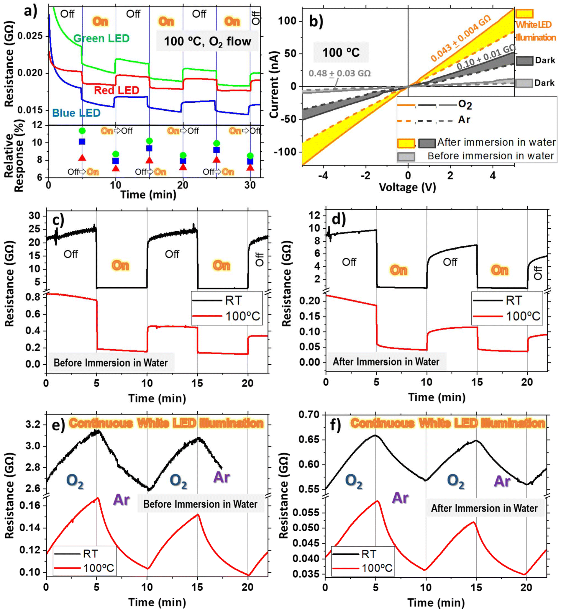
As demonstrated in Fig. 5, light-induced responsivity can be used to switch ON and OFF the sensor response, consequently increasing their lifetime. To prove this idea, illumination experiments were carried out using a series of three LEDs: blue, green, and red at emission wavelengths of 465, 530, and 635 nm, respectively, with significantly lower powers than the Xe lamp used in the previous experiments (see Table S2†). The switching evolution is shown in Fig. 6(a) and was measured at 100 °C under a constant oxygen flux atmosphere for the ONT-based sensor. It may be appreciated that once the LEDs were turned ON, the resistance reduced quickly, and when turned OFF, the opposite occurred. Note that the resistance changes were not as pronounced as in the previous case due to the lower power of the LEDs. The bottom part of Fig. 6(a) shows the relative response calculated from the previous curves. To minimise the drift effect, the relative response was calculated by using the signal some seconds before the illumination change and after 20 seconds. For every LED, two different responses were obtained separately, distinguishing between the “Off–On” and “On–Off” transitions (note that these transitions occur at 5, 15, 25 and 10, 20, 30 minutes, respectively). The change in the sensor's response is not identical for the two cases, as can be observed in the figure. The relative response is systematically lower for the On–Off steps for the three LEDs.
 | ||
| Fig. 6 (a) Sensor response at 100 °C to oxygen under intermittent illumination with red, green or blue LEDs (top) and the relative response (bottom). (b) I–V curves of the ONT sensors before (green lines) and after the water immersion treatment (black and red lines), both under white LED illumination (black) and in the dark (green and red) at 100 °C. The I–V curves under O2 and Ar atmospheres (after 10 minutes of gas flow) are shown with solid and dashed lines, respectively. Resistance evolution of the sensors at a constant O2 flow at RT (black line) and 100 °C (red) under intermittent white LED illumination every 5 minutes before (c) and after (d) the water immersion treatment. Resistance evolution under continuous white LED illumination upon modifying the atmosphere from oxygen to argon in cycles of 5 minutes at RT (black curve) and 100 °C (red curve) before (e) and after (f) the water immersion treatment. | ||
One remarkable characteristic is that H2Pc presents a visible absorption band at 620 nm, very close to the red LED wavelength, as shown in Fig. S7.† From this figure, noticeable changes in the resistance evolution for the different wavelengths of the LEDs are expected since the H2Pc ONTs absorb a significantly smaller amount of light at the green and blue wavelengths than the red one. According to the UV-Vis transmittance and the emission spectra of the LEDs (both shown in Fig. S7†) and the power densities listed in Table S2,† the red LED should exhibit the highest photoconductivity, but this has not been the case. While the responses are comparable, the red LED consistently produces the smallest response, and the green LED produces the highest change across all cycles, regardless of whether the transitions are “On–Off” or “Off–On”. This behaviour does not correlate with the absorption band of the ONTs or with the power of the LEDs, indicating that additional effects such as sensor drifting need to be considered.
The response times for the sensor upon illumination with the three LEDs have also been calculated by fitting with a two-exponential decay curve, and are shown in Fig. S8.† For all wavelengths studied, similar response times were observed, with two distinct components: t1 (faster) and t2 (slower), the latter with the highest contribution (more than 95% for all the cases). As observed from the relative response in Fig. 6(a), the response times differed significantly between the “Off–On” and “On–Off” transitions, with the latter showing slower t1 and faster t2. It should be noted that a drift may influence these fits, especially the differences between “Off–On” and “On–Off” transitions, and therefore, the response times should be interpreted qualitatively.
Since no significant wavelength dependence was observed (neither in the relative response nor the response time), photoconductivity experiments with the LEDs were performed using a combination of the three previously used LEDs (R + G + B), giving an overall power density of 11.2 mW cm−2 (see Table S2†). Fig. 6(b) presents the I–V characteristics of the ONT-based sensor before (grey lines) and after water immersion (black and orange lines), both under white LED illumination (orange) and in the dark (grey and black) at 100 °C. As mentioned above, the immersion process induces an improved interconnection between the branches, producing a significant decrease in the resistance of the sensor device, from 0.48 to 0.1 GΩ, which further decreased to 0.04 GΩ under white LED illumination (measured under an oxygen atmosphere). Fig. 6(b) also shows the I–V curves under O2 and Ar atmospheres (after ca. 10 minutes of exposure) with solid and dashed lines, respectively. Though the first impression from the figure is that the illuminated ONTs after water immersion show the highest variation, the three cases have approximately the same response of about 35–45% when the atmosphere varies between argon and oxygen (in this case, no precise response could be given due to the lack of measurement cycles). This would indicate that although the resistance is lower for devices subjected to immersion in water and LED illumination, the response is similar for the three cases.
The resistance evolution under intermittent LED illumination (every 5 minutes) is presented in Fig. 6(c) and (d) before and after water immersion, respectively. Please note that the starting resistance is not as low as in Fig. 6(a) because the white LED experiments performed at 100 °C started 10 minutes after reaching the target temperature, while in the rest, the stabilisation time was above 1 hour. The figure shows the evolution of the sensor at RT (black curve) and 100 °C (red). It can be noted that there is a fast resistance change upon illumination in all cases, where the change is significantly higher for the RT experiments. In these measurements at RT (black curves in Fig. 6c and d), the resistance difference between the OFF/ON states (understanding the sensor as a photodetector) gives responses of 87 ± 2 and 89 ± 2%, while at 100 °C (red curves), they are 68 ± 5 and 61 ± 6% for the devices measured before and after water immersion treatment, respectively. These results are similar to those shown in Fig. 5 and 6(a) and consistent with photoconduction switching, which has also proven to be prompt and reproducible with the turning ON and OFF of light (Fig. 6c and d), implying not only a fast photoresponse but also the high stability of the materials when operated under ambient conditions.
The reported photoconductivity can be used to decrease the resistance of the sensor devices, but is the sensitivity of the sensor modified upon LED illumination? To answer this question, Fig. 6(e) and (f) show the evolution of the resistance under continuous white LED illumination upon modifying the atmosphere from oxygen to argon (cycles of 5 minutes) at RT (black curve) and 100 °C (red curve) before (e) and after (f) the water immersion treatment. Starting from the 100 °C experiments, the resistance evolution depicts a similar shape, as shown in Fig. (5c), to the dark case. The main difference is a higher sensitivity in the white LED illumination experiments for both before and after water immersion treatment, showing a response of 37 ± 2 and 35 ± 4%, respectively, while in the dark case (only measured before water immersion treatment, as shown in Fig. 5c) a four times less response of 9 ± 1% is observed. This experiment proves that LED illumination enhances the sensor response.
Moreover, the RT experiments revealed a striking result; while in the Ar/O2 cycling experiments in the dark, the sensor shows no response (not possible to quantify), illumination with a low-power LED enables the sensing capability of the devices. The illumination increases the response from nearly zero to 16 ± 1% and 14 ± 1% before and after water immersion treatment, respectively. It is important to remark that the enhanced response for the RT case under low-power white LED illumination proves that the sensor can be switched ON and OFF by simply illuminating with an LED together with a reduction of the resistance. To our knowledge, these are the first results of a visible range lighting strategy to improve the response of organic-based sensors, opening a new path toward the exploitation of semiconducting organic nanowires as low-cost and low-power sensors since they can be switched ON and OFF periodically simply by illumination with a LED, diminishing their consumption since they can operate at RT.
Conclusions
The direct fabrication of H2Pc nanowires and nanotrees on preformed interdigitated-based sensors has been successfully addressed. A high-density nanoforest was obtained by a combination of vacuum/plasma deposition methods, namely magnetron sputtering for the seeds, physical vapour deposition for the nanowires and soft plasma etching for the formation of crystallisation sites along the primary ONWs to induce the growth of secondary ones. The entire process has been carried out at mild temperatures (<200 °C) on commercial substrates consisting of interdigitated electrodes, reducing resistivity due to the contact of the ONWs or ONTs. The resistance was significantly lower for the ONT sample, indicating a higher number of contacts between the branches. The nanowire contact could be further improved by a simple water immersion protocol for both the ONWs and ONTs, producing the laydown and entanglement of the flexible nanostructures, which results in a significant decrease in the resistivity of the sensor. Moreover, as expected for a semiconductor, a temperature-dependent resistance was observed. However, the reduction of the resistivity observed at 100 °C is much higher than that expected, considering the bulk resistivity at this temperature, especially for the ONT case, indicating a decrease in the contact resistance between the wires induced by the temperature.The response to oxygen is negligible at room temperature for both ONW and ONT-based sensors. However, contrary to expectations, a clear response is observed at higher temperatures (50 and 100 °C). Nevertheless, as reported by other authors, this response remains very weak even at 100 °C due to the slow diffusion of gases in crystalline H2Pc thin films.67,69 Thus, the augmented response at moderate temperatures (50–100 ºC) for our ONW and ONT can be attributed to the high specific area of these 1D and 3D nanostructures, which effectively enhances the oxygen doping of the organic nanostructures. Moreover, the enhancement in the oxygen response by light illumination was quite significant. For the three temperatures studied, the effect of illumination on the conductivity was independent of the temperature of the samples. This result indicates that the sensors can work at room temperature under illumination, opening a new way for low-cost and long-lasting devices since room temperature operation usually preserves the sensor performance of organic materials.
Therefore, additional experiments with more feasible light sources, such as low-power LEDs, were performed. The spectral dependency on illumination was tested with three different wavelengths (blue, green and red), showing a similar response even when the red LED overlapped with the absorption band of the H2Pc molecule. In any case, the enhanced conductivity induced by a low-power LED light can be used to switch ON and OFF the sensor response even at RT. Additionally, this type of device has a high potential for low-power electronics since the sensor is at room temperature (no heating is necessary), which allows it to work under non-constant operation. This latter aspect will permit an intermittent operation of the sensor, switching ON for some seconds under LED illumination to sense the concentration of a particular analyte.
The promising sensitivity enhancements achieved with metal-free phthalocyanine, facilitated by nanostructuration and photoenhanced effects, suggest that incorporating metallated phthalocyanines or porphyrins could further improve selectivity toward specific analytes. These precursors are also compatible with the direct synthesis methodology for organic nanowires and nanotrees on preformed interdigitated electrodes, thus paving the way for future sensor devices with high selectivity, sensitivity and response times, which can detect a wider range of oxidative gases. It is important to mention that the nanotree architecture also allows combining different molecules to form primary and secondary nanowires, which might provide a successful approach to fabricating 1D multi-sensors.
Author contributions
A. Borrás, A. Barranco, and J. R. Sanchez-Valencia: conceptualisation. A. Borrás and A. Barranco: funding acquisition. A. Borrás and J. R. Sanchez-Valencia: writing the original draft. A. N. Filippin, A. Campos-Lendinez, J. Delgado-Alvarez, and G. Moreno-Martinez: sample fabrication and sensor assembly. A. N. Filippin, A. Campos-Lendinez, J. Castillo-Seoane, V. J. Rico, V. F. Godinho, and J. R. Sanchez-Valencia: sensor characterisation. All the authors were involved in the article's investigation, methodology, validation, review, and editing.Data availability
The authors confirm that the data supporting the findings of this study are available within the article and its ESI.†Conflicts of interest
There are no conflicts to declare.Acknowledgements
The authors thank the projects PID2022-143120OB-I00, TED2021-130916B-I00, and PCI2024-153451 funded by MCIN/AEI/10.13039/501100011033 and “ERDF (FEDER)” A way of making Europe, Fondos NextgenerationEU and Plan de Recuperación, Transformación y Resiliencia. Project ANGSTROM was selected in the Joint Transnational Call 2023 of M-ERA.NET 3, which is an EU-funded network of about 49 funding organisations (Horizon 2020 grant agreement No 958174). The project leading to this article has received funding from the EU H2020 program under grant agreement 851929 (ERC Starting Grant 3DScavengers).References
- Y. Xiao, H. Li, C. Wang, S. Pan, J. He, A. Liu, J. Wang, P. Sun, F. Liu and G. Lu, Adv. Sens. Res., 2024, 3, 2300035 Search PubMed.
- N. Goel, K. Kunal, A. Kushwaha and M. Kumar, Eng. Rep., 2023, 5, e12604 CrossRef.
- Z. Wang, M. Bu, N. Hu and L. Zhao, Composites, Part B, 2023, 248, 110378 CrossRef.
- S. Sardana, H. Kaur, B. Arora, D. K. Aswal and A. Mahajan, ACS Sens., 2022, 7, 312–321 CrossRef.
- S. Sardana and A. Mahajan, ACS Appl. Nano Mater., 2023, 6, 469–481 CrossRef.
- S. Yuvaraja, A. Nawaz, Q. Liu, D. Dubal, S. G. Surya, K. N. Salama and P. Sonar, Chem. Soc. Rev., 2020, 49, 3423–3460 RSC.
- B. King and B. H. Lessard, J. Mater. Chem. C, 2024, 12, 5654–5683 RSC.
- Z. Shen, W. Huang, L. Li, H. Li, J. Huang, J. Cheng and Y. Fu, Small, 2023, 19, 2302406 Search PubMed.
- C. M. Boutry, Y. Kaizawa, B. C. Schroeder, A. Chortos, A. Legrand, Z. Wang, J. Chang, P. Fox and Z. Bao, Nat. Electron., 2018, 1, 314–321 CrossRef.
- J. Polena, D. Afzal, J. H. L. Ngai and Y. Li, Chemosensors, 2022, 10, 12 CrossRef.
- Y. Huang, X. Fan, S. Chen and N. Zhao, Adv. Funct. Mater., 2019, 29, 1808509 CrossRef.
- G. Simone, M. J. Dyson, S. C. J. Meskers, R. A. J. Janssen and G. H. Gelinck, Adv. Funct. Mater., 2020, 30, 1904205 CrossRef.
- X. Chen, W. Mao, W. Zhou, P. Huang, H. Liu, X. Wang, Z. Liang, Q. Yang, Y. Chen, G. Zhou and J. Xu, ACS Appl. Mater. Interfaces, 2024, 16, 57512–57523 CrossRef PubMed.
- H. Liu, J. Song, Z. Zhao, S. Zhao, Z. Tian and F. Yan, Adv. Sci., 2024, 11, 2305347 CrossRef CAS.
- J. V. Dcosta, D. Ochoa and S. Sanaur, Adv. Sci., 2023, 10, 2302752 CrossRef PubMed.
- W.-D. Li, K. Ke, J. Jia, J.-H. Pu, X. Zhao, R.-Y. Bao, Z.-Y. Liu, L. Bai, K. Zhang, M.-B. Yang and W. Yang, Small, 2022, 18, 2103734 CrossRef CAS PubMed.
- M. Wu, S. Hou, X. Yu and J. Yu, J. Mater. Chem. C, 2020, 8, 13482–13500 RSC.
- H. F. Iqbal, Q. Ai, K. J. Thorley, H. Chen, I. McCulloch, C. Risko, J. E. Anthony and O. D. Jurchescu, Nat. Commun., 2021, 12, 2352 CrossRef CAS PubMed.
- J.-H. Kwon, M.-H. Kim and J.-H. Bae, J. Mater. Chem. C, 2023, 12, 29–49 RSC.
- K. Tie, J. Qi, Y. Hu, Y. Fu, S. Sun, Y. Wang, Y. Huang, Z. Wang, L. Yuan, L. Li, D. Wei, X. Chen and W. Hu, Sci. Adv., 2024, 10, eadn5964 CrossRef CAS.
- S. Mandal, M. Banerjee, S. Roy, A. Mandal, A. Ghosh, B. Satpati and D. K. Goswami, ACS Appl. Mater. Interfaces, 2019, 11, 4193–4202 CrossRef CAS.
- H. S. Nalwa, in Handbook of Surfaces and Interfaces of Materials, Academic Press, Burlington, 2001, pp. xxv–xxviii Search PubMed.
- J. Sheng, H.-J. Jeong, K.-L. Han, T. Hong and J.-S. Park, J. Inf. Disp., 2017, 18, 159–172 Search PubMed.
- D. Gounden, N. Nombona and W. E. van Zyl, Coord. Chem. Rev., 2020, 420, 213359 Search PubMed.
- R. Song, Z. Wang, X. Zhou, L. Huang and L. Chi, ChemPlusChem, 2019, 84, 1222–1234 CrossRef CAS PubMed.
- S. Ganesh Moorthy, J. Arvidson, R. Meunier-Prest, H. Wang and M. Bouvet, ACS Sens., 2024, 9, 883–894 Search PubMed.
- F. I. Bohrer, A. Sharoni, C. Colesniuc, J. Park, I. K. Schuller, A. C. Kummel and W. C. Trogler, J. Am. Chem. Soc., 2007, 129, 5640–5646 Search PubMed.
- M. M. El-Nahass, A. M. Farid, A. A. Attia and H. A. M. Ali, Appl. Surf. Sci., 2006, 252, 7553–7561 Search PubMed.
- R. Saini, A. Mahajan, R. K. Bedi, D. K. Aswal and A. K. Debnath, RSC Adv., 2014, 4, 15945–15951 Search PubMed.
- A. E. Pochtennyi and V. K. Dolgiy, Nanoscience and Technology: An International Journal, 2019, 10, 311–320 Search PubMed.
- S. Kumar, A. K. Sharma, M. K. Sohal, D. P. Sharma, A. K. Debnath, D. K. Aswal and A. Mahajan, Sens. Actuators, B, 2021, 327, 128925 CrossRef CAS.
- J. D. Wright, Prog. Surf. Sci., 1989, 31, 1–60 Search PubMed.
- R. D. Gould, Coord. Chem. Rev., 1996, 156, 237–274 Search PubMed.
- A. A. El-Saady, N. Roushdy, A. A. M. Farag, M. M. El-Nahass and D. M. Abdel Basset, Opt. Quantum Electron., 2023, 55, 662 CrossRef CAS.
- P. Powroźnik, B. Solecka, P. Pander, W. Jakubik, F. B. Dias and M. Krzywiecki, Sensors, 2022, 22, 9947 CrossRef PubMed.
- J. P. Contour, P. Lenfant and A. K. Vijh, J. Catal., 1973, 29, 8–14 CrossRef CAS.
- S. Y. Flores, J. Gonzalez-Espiet, J. Cintrón, N. D. J. Villanueva, F. E. Camino, K. Kisslinger, D. M. P. Cruz, R. D. Rivera and L. F. Fonseca, ACS Appl. Nano Mater., 2022, 5, 4688–4699 CrossRef CAS.
- Z.-L. Gong, Y. Guo and Y.-W. Zhong, Mater. Chem. Front., 2023, 7, 6281–6304 RSC.
- A. Kumar, R. Meunier-Prest and M. Bouvet, Sensors, 2020, 20, 4700 CrossRef CAS PubMed.
- D. Klyamer, R. Shutilov and T. Basova, Sensors, 2022, 22, 895 CrossRef CAS.
- L. Xiao, S. Yu, Q. Cui, J. Liu, G. Liang, Y. Li and G.-J. Zhang, Sens. Actuators, B, 2024, 406, 135402 CrossRef CAS.
- P. Feng, F. Shao, Y. Shi and Q. Wan, Sensors, 2014, 14, 17406–17429 Search PubMed.
- T. Shaymurat, Q. Tang, Y. Tong, L. Dong and Y. Liu, Adv. Mater., 2013, 25, 2376–2376 Search PubMed.
- M. Sangchap, H. Hashtroudi, T. Thathsara, C. J. Harrison, P. Kingshott, A. E. Kandjani, A. Trinchi and M. Shafiei, Int. J. Hydrogen Energy, 2024, 50, 1443–1457 Search PubMed.
- J. Ding, Z. Zheng, Z. Song, S. Ding, J. Wen, K. Liu, C. Zhang and H. Li, Mater. Des., 2023, 234, 112360 Search PubMed.
- A. Borras, M. Aguirre, O. Groening, C. Lopez-Cartes and P. Groening, Chem. Mater., 2008, 20, 7371–7373 CrossRef CAS.
- A. Borras, O. Gröning, M. Aguirre, F. Gramm and P. Gröning, Langmuir, 2010, 26, 5763–5771 CrossRef CAS.
- M. Alcaire, J. R. Sanchez-Valencia, F. J. Aparicio, Z. Saghi, J. C. Gonzalez-Gonzalez, A. Barranco, Y. O. Zian, A. R. Gonzalez-Elipe, P. Midgley, J. P. Espinos, P. Groening and A. Borras, Nanoscale, 2011, 3, 4554 RSC.
- A. Borras, P. Gröning, J. R. Sanchez-Valencia, A. Barranco, J. P. Espinos and A. R. Gonzalez-Elipe, Langmuir, 2010, 26, 1487–1492 CrossRef CAS PubMed.
- J. Castillo-Seoane, J. Gil-Rostra, V. López-Flores, G. Lozano, F. J. Ferrer, J. P. Espinós, K. (Ken) Ostrikov, F. Yubero, A. R. González-Elipe, Á. Barranco, J. R. Sánchez-Valencia and A. Borrás, Nanoscale, 2021, 13, 13882–13895 RSC.
- M. Macias-Montero, A. N. Filippin, Z. Saghi, F. J. Aparicio, A. Barranco, J. P. Espinos, F. Frutos, A. R. Gonzalez-Elipe and A. Borras, Adv. Funct. Mater., 2013, 23, 5981–5989 CrossRef.
- A. N. Filippin, J. R. Sanchez-Valencia, X. Garcia-Casas, V. Lopez-Flores, M. Macias-Montero, F. Frutos, A. Barranco and A. Borras, Nano Energy, 2019, 58, 476–483 CrossRef.
- A. N. Filippin, M. Macias-Montero, Z. Saghi, J. Idígoras, P. Burdet, J. R. Sanchez-Valencia, A. Barranco, P. A. Migdley, J. A. Anta and A. Borras, Sci. Rep., 2017, 7, 9621 CrossRef.
- A. N. Filippin, V. López-Flores, T. C. Rojas, Z. Saghi, V. J. Rico, J. R. Sanchez-Valencia, J. P. Espinós, A. Zitolo, M. Viret, P. A. Midgley, A. Barranco and A. Borras, Chem. Mater., 2018, 30, 879–887 Search PubMed.
- A. Nicolas Filippin, J. R. Sanchez-Valencia, J. Idígoras, T. C. Rojas, A. Barranco, J. A. Anta and A. Borras, Nanoscale, 2017, 9, 8133–8141 RSC.
- N. Filippin, J. Castillo-Seoane, M. C. López-Santos, C. T. Rojas, K. Ostrikov, A. Barranco, J. R. Sánchez-Valencia and A. Borrás, ACS Appl. Mater. Interfaces, 2020, 12, 50721–50733 CrossRef.
- J. Castillo-Seoane, L. Contreras-Bernal, T. C. Rojas, J. P. Espinós, A.-F. Castro-Méndez, J.-P. Correa-Baena, A. Barranco, J. R. Sanchez-Valencia and A. Borras, Adv. Funct. Mater., 2024, 34, 2403763 CrossRef.
- F.-X. Wang, Y.-Q. Liu, H.-D. Wu, Y. Xiao and G.-B. Pan, J. Mater. Chem. C, 2012, 1, 422–425 RSC.
- Y. Alfredsson, B. Brena, K. Nilson, J. Åhlund, L. Kjeldgaard, M. Nyberg, Y. Luo, N. Mårtensson, A. Sandell, C. Puglia and H. Siegbahn, J. Chem. Phys., 2005, 122, 214723 CrossRef PubMed.
- K. Nilson, J. Åhlund, M.-N. Shariati, J. Schiessling, P. Palmgren, B. Brena, E. Göthelid, F. Hennies, Y. Huismans, F. Evangelista, P. Rudolf, M. Göthelid, N. Mårtensson and C. Puglia, J. Chem. Phys., 2012, 137, 044708 CrossRef.
- Y. Kim, S.-K. Kang, N.-C. Oh, H.-D. Lee, S.-M. Lee, J. Park and H. Kim, ACS Appl. Mater. Interfaces, 2019, 11, 38902–38909 CrossRef PubMed.
- T. N. Krauss, E. Barrena, T. Lohmüller, J. P. Spatz and H. Dosch, Phys. Chem. Chem. Phys., 2011, 13, 5940–5944 RSC.
- M. Alcaire, F. J. Aparicio, J. Obrero, C. López-Santos, F. J. Garcia-Garcia, J. R. Sánchez-Valencia, F. Frutos, K. (Ken) Ostrikov, A. Borrás and A. Barranco, Adv. Funct. Mater., 2019, 29, 1903535 CrossRef.
- L. R. Fleet, J. Stott, B. Villis, S. Din, M. Serri, G. Aeppli, S. Heutz and A. Nathan, ACS Appl. Mater. Interfaces, 2017, 9, 20686–20695 CrossRef.
- K. Toyota, J. Hasegawa and H. Nakatsuji, J. Phys. Chem. A, 1997, 101, 446–451 CrossRef.
- Y. Ishida, J. K. Jung, M. S. Kim, J. Kwon, Y. S. Kim, D. Chung, I. Song, C. Kim, T. Otsu and Y. Kobayashi, Commun. Phys., 2020, 3, 1–8 CrossRef.
- E. van Faassen and H. Kerp, Sens. Actuators, B, 2003, 88, 329–333 CrossRef.
- D. Tomecek, M. Hruska, P. Fitl, J. Vlcek, E. Maresova, S. Havlova, L. Patrone and M. Vrnata, ACS Sens., 2018, 3, 2558–2565 Search PubMed.
- K. Kudo, T. Sumimoto, K. Hiraga, S. Kuniyoshi and K. Tanaka, Jpn. J. Appl. Phys., 1997, 36, 6994 CrossRef.
- G. A. Kumar, J. Thomas, N. George, N. V. Unnikrishnan, P. Radhakrishnan, V. P. N. Nampoori and C. P. G. Vallabhan, J. Mater. Sci., 2000, 35, 2539–2542 CrossRef.
Footnote |
| † Electronic supplementary information (ESI) available: Schemes of ONW growth, sensor set-up, additional SEM, Raman, XPS, electrical and sensor response characterization, light power densities and spectral distribution of the illumination sources. See DOI: https://doi.org/10.1039/d4nr04761c |
| This journal is © The Royal Society of Chemistry 2025 |