
 Open Access Article
 This Open Access Article is licensed under a Creative Commons Attribution-Non Commercial 3.0 Unported Licence
Germanium nanocrystal non-volatile memory devices: fabrication, charge storage mechanism and characterization
Wai Kin
Chim

Department of Electrical and Computer Engineering, National University of Singapore, 4 Engineering Drive 3, Singapore 117583. E-mail: elecwk@nus.edu.sg
First published on 16th January 2025
Abstract
The widespread proliferation and increasing use of portable electronic devices and wearables, and the recent developments in artificial intelligence and internet-of-things, have fuelled the need for high-density and low-voltage non-volatile memory devices. Nanocrystal memory, an emergent non-volatile memory (NVM) device that makes use of the Coulomb blockade effect, can potentially result in the scaling of the tunnel dielectric layer to a very small thickness. Since the nanocrystals are electrically isolated, potential charge leakage paths via localized defects in the thin tunnel dielectric can be substantially reduced, unlike that in a continuous polysilicon floating gate structure. The equivalent oxide thickness of the tunnel dielectric layer can be further reduced by using high dielectric constant materials to replace silicon dioxide, thus giving rise to faster program/erase during device operation and better charge retention performance. In this review on germanium (Ge) nanocrystal NVM devices, a brief historical perspective of semiconductor NVM devices will first be presented. Fabrication techniques for synthesizing Ge nanocrystals and those for Ge nanocrystal capacitor and transistor devices in a tri-layer insulator gate stack structure will then be presented. Investigations into the charge storage mechanism and electrical performance of Ge nanocrystal memory devices will be discussed. The application of a scanning probe microscopy-based nano-characterization method, that of scanning capacitance spectroscopy/microscopy, to analyze carrier charging in Ge nanodots and the passivation of hole and electron traps after forming gas annealing will be highlighted. This has led to a better understanding of the charge storage mechanism in the Ge nanocrystals. The use of high dielectric constant materials in the tri-layer gate structure to minimize Ge penetration into the substrate during the high temperature annealing synthesis step will also be presented in this article. Traps/defects within the Ge nanocrystals play an important role in the charge storage and retention mechanism. This article will also show how the trap energy level could be modulated using high dielectric constant materials in the tunnel dielectric and cap oxide layers for improved device performance.
 Wai Kin Chim | Wai Kin Chim received his B.Eng. and Ph.D. degrees in electrical engineering from the National University of Singapore (NUS). He is currently teaching at the Department of Electrical and Computer Engineering, College of Design and Engineering, NUS. His research interests are in the growth and characterization of nanostructures for memory applications (e.g., nanocrystal memory, SONOS and RRAM), various areas of MOS technology (e.g., high-k and complex metal oxides, MOS device physics and reliability), photon emission microscopy and scanning capacitance microscopy. |
1. Introduction
Nanostructures, in the form of nanodots or nanocrystals with typical dimensions of about 1 to 100 nm, have attracted much attention due to their superior properties as compared to bulk structures. For semiconductor nanodots, desired quantum effects arise for structures with dimensions of ∼10–100 nm and containing somewhere between a thousand to a million atoms in a crystalline lattice.1 Nanocrystals, or nanodots, could be employed in transistor memory devices for charge storage.2–7 This is important for extending the device feature size scaling of electronic memory devices. The widespread proliferation and increasing use of portable electronic devices and wearables, and the recent developments in artificial intelligence and internet-of-things, have resulted in the need for high-density and low-voltage non-volatile memory devices. The conventional polysilicon floating-gate memory structure was unable to employ an ultra-thin tunnel oxide due to charge retention reliability issues. Nanocrystal memory, an emergent non-volatile memory (NVM) structure that makes use of the Coulomb blockade effect,8–10 can potentially result in the scaling of the tunnel dielectric to a very small thickness. Since the nanocrystals are electrically isolated, potential charge leakage paths via localized defects in the thin tunnel oxide can be substantially decreased. The equivalent oxide thickness (EOT) of the tunnel dielectric layer can be further reduced by using high dielectric constant materials to replace silicon dioxide, thus giving rise to better charge retention performance and faster program/erase during device operation. Flash non-volatile memory devices, with embedded germanium (Ge) or silicon (Si) nanocrystals, are also compatible with existing complementary metal–oxide–semiconductor (CMOS) fabrication processes.Replacing the polysilicon floating gate layer of an existing flash memory device structure with silicon nanocrystals for improved reliability and electrical performance, such as improved charge retention duration and programming at low voltages and faster speed, was first demonstrated by Tiwari and co-workers.2,11,12 This has given rise to much interest in nanocrystal flash memory device applications. King et al. also demonstrated a nanocrystalline Ge memory device with superior programming speed and superior retention time.13 Earlier studies on flash memory devices have been concentrated on using either nanocrystalline Si or Ge to replace the continuous floating gate layer. Over the years, other groups have also proposed using metal dots, such as Au, Ag, W, Pt and Sn, for charge storage.14–16 The advantage of using metal nanodots is the creation of an asymmetrical barrier between the substrate and the storage nodules by engineering the metal work function, thus resulting in a smaller potential barrier for programming and a larger barrier for charge retention.14,15 Notwithstanding, introducing metal nanodots could compromise the compatibility to existing CMOS fabrication processes.
In this article on Ge nanocrystal NVM devices, a brief historical perspective of semiconductor NVM memory devices will first be presented. Fabrication techniques for synthesizing Ge nanocrystals and those for Ge nanocrystal capacitor and transistor devices in a tri-layer insulator gate stack structure will then be presented. Investigations into the charge storage mechanism and electrical performance of Ge nanocrystal memory devices will be discussed. The application of a scanning probe microscopy-based nano-characterization method, that of scanning capacitance spectroscopy/microscopy, to analyze carrier charging in Ge nanodots and the passivation of hole and electron traps after forming gas annealing will be highlighted. This has resulted in a better understanding of the charge storage mechanism in the Ge nanocrystals. The use of high dielectric constant materials in the Ge nanocrystal memory tri-layer gate structure for improved device performance will also be presented.
2. Brief historical perspective of semiconductor non-volatile memory devices
The history of semiconductor non-volatile memory (NVM) devices can be dated back to 1967, when the “floating gate” NVM structure was introduced by Kahng and Sze.17 In that historical work, the memory device consisted of a conventional metal–oxide–semiconductor field-effect transistor (MOSFET) with an embedded metal floating gate. The floating gate transistor structure therefore consists of two gates (i.e., top and bottom gates) above the tunnel (or gate) oxide and on the same side of the MOSFET. The bottom gate, or the floating gate, is placed directly above the tunnel oxide and is not connected electrically to the external world; hence the term “floating gate”. The top gate, electrically isolated from the bottom gate by a blocking or cap oxide and connected electrically to the external world, is termed the “control gate”. The floating gate served as a storage site for electrons that were injected from the substrate across the thin (3 nm thickness) tunnel oxide during the programming phase. Due to its poor charge retention capability, the initial metal floating gate design has been modified by either introducing a charge trapping dielectric layer to replace the metal layer or to use a thicker tunnel barrier together with a polysilicon layer to replace the metal floating gate. The structures that use the former and latter methods are denoted as “charge trapping” and “floating gate” devices, respectively. The floating gate device later evolved to become the mainstream product in the NVM market because of the following reasons. First, its fabrication process is compatible with conventional CMOS processing. Second, the use of a thicker oxide as the tunnel barrier gives better charge retention performance and good read-disturb tolerance. However, the use of a thicker tunnel barrier in a floating gate device would require a large charging voltage to achieve high programming efficiency. A way to avoid this, and still achieve a high charging efficiency, is the implementation of avalanche injection of carriers in the drain region of the memory transistor, thus resulting in the introduction of the FAMOS (![[f with combining low line]](https://www.rsc.org/images/entities/char_0066_0332.gif) loating gate
loating gate ![[a with combining low line]](https://www.rsc.org/images/entities/char_0061_0332.gif) valanche injection
valanche injection ![[m with combining low line]](https://www.rsc.org/images/entities/char_006d_0332.gif) etal–
etal–![[o with combining low line]](https://www.rsc.org/images/entities/char_006f_0332.gif) xide–
xide–![[s with combining low line]](https://www.rsc.org/images/entities/char_0073_0332.gif) emiconductor) structure.18 The FAMOS combines the floating gate concept with avalanche injection of electrons from the surface depletion layer of the p–n junction at the drain region of the memory transistor. On the other hand, the “charge trapping” device or the SONOS (polyilicon-blocking xide-silicon
emiconductor) structure.18 The FAMOS combines the floating gate concept with avalanche injection of electrons from the surface depletion layer of the p–n junction at the drain region of the memory transistor. On the other hand, the “charge trapping” device or the SONOS (polyilicon-blocking xide-silicon ![[n with combining low line]](https://www.rsc.org/images/entities/char_006e_0332.gif) itride-tunnel xide-ilicon) structure19 found only niche application, primarily in space application and strategic areas, due to the difficulty of fabricating thin layers of silicon oxide and silicon nitride in the 1970s. SONOS memory uses a MOSFET structure with the addition of a thin silicon nitride layer above the gate oxide or tunnel oxide of the transistor. The silicon nitride layer is a non-conductive dielectric but contains a large number of charge trapping sites that are able to hold on to electrostatic charges from the trapped charge carriers during the programming or charging phase of SONOS memory. The silicon nitride layer is electrically isolated from the top gate electrode through a blocking oxide or cap oxide layer. With progress in fabrication technologies, the SONOS structure has also become a potential NVM candidate to overcome the scaling limitations, especially the requirement of a thick tunnel barrier, of the floating gate structure.
itride-tunnel xide-ilicon) structure19 found only niche application, primarily in space application and strategic areas, due to the difficulty of fabricating thin layers of silicon oxide and silicon nitride in the 1970s. SONOS memory uses a MOSFET structure with the addition of a thin silicon nitride layer above the gate oxide or tunnel oxide of the transistor. The silicon nitride layer is a non-conductive dielectric but contains a large number of charge trapping sites that are able to hold on to electrostatic charges from the trapped charge carriers during the programming or charging phase of SONOS memory. The silicon nitride layer is electrically isolated from the top gate electrode through a blocking oxide or cap oxide layer. With progress in fabrication technologies, the SONOS structure has also become a potential NVM candidate to overcome the scaling limitations, especially the requirement of a thick tunnel barrier, of the floating gate structure.
In 1980, researchers at Intel proposed the “FLOating gate Tunnel OXide” (FLOTOX) structure which used electrical signals to perform byte-by-byte erasing without having to erase the entire NVM chip during reprogramming.20 Today, the most widespread NVM array organization is the flash memory, in which a byte-selectable write operation is combined with sector “flash” erasing. The flash memory was first introduced by F. Masuoka in 1984 while working at Toshiba.21 The name “flash” was used to denote the fact that the entire memory sector could be erased in a single operation.
More recently, researchers have investigated the potential of charge trapping devices to replace the floating gate device, with two strong candidates having emerged. These are the nitride-type memory, based on the SONOS structure as mentioned earlier,18 and the nanocrystal memory.2–7,11–16 Nanocrystal memory structures use a charge storage layer consisting of nano-islands of a crystalline material (semiconductor or metal), sometimes called nano-dots or nanocrystals. Each nano-dot will typically store a single charge carrier or several charge carriers, which will collectively control the channel conductivity of the memory structure. Nanocrystal memory offers several advantages over the nitride-type memory device. First, due to the distributed nature of nanocrystals, one weak spot in the tunnel barrier does not necessarily cause the device to fail catastrophically. For the case of the nitride-type memory device, such a weak spot will possibly cause the device to fail, especially if the stored charges are connected to this weak spot through lateral leakage or conduction paths. Due to this reason, the nanocrystal memory can allow further scaling of the tunnel oxide/barrier dimension. The scaling of the tunnel barrier thickness will in turn lead to a reduction in the charging (supply) voltage to maintain the same electric field magnitude across the tunnel oxide. Second, since the charges are localized in each individual nanocrystal and there are negligible interacting paths in-between the nanocrystals, the nanocrystal memory does not suffer from lateral hoping or percolative leakage as observed in the nitride-type memory device. Another attractive feature in nanocrystal memory is the possible use of quantum confinement effects in charge storage.8–10,12 Quantum confinement effects in nanocrystals (i.e., bandgap widening and energy quantization) can be exploited in small size nanocrystal devices. Another feature is the weak dependency of the drain-to-nanocrystal coupling ratio in nanocrystal memory, which means a smaller drain-induced barrier lowering effect. Other attractive advantages include the potential of achieving multi-bit storage using Coulomb blockade in nanocrystals and the larger carrier capture cross section in nanocrystals that would result in a higher trapping efficiency.
3. Fabrication of germanium nanocrystal memory structures
3.1. Synthesis methods for germanium nanocrystals
Nanocrystalline Ge, although posing several fabrication challenges, is a suitable candidate to replace the continuous polysilicon floating gate for flash memory devices. The smaller band gap of Ge, as compared to the Si substrate, results in a higher confinement barrier for charge retention and a smaller barrier for program and erase modes, similar to metal nanodots but avoiding the CMOS compatibility issue.22 However, the fabrication of Ge nanocrystals is more difficult than Si nanocrystals due to the lower evaporation temperature and difference in the surface energy of Ge with respect to silicon oxide. Researchers have demonstrated various methods for synthesizing Ge nanocrystals, which include pyrolysis,23,24 sol–gel synthesis,25 spark processing,26 pulse laser ablation,27,28 molecular beam epitaxy,29,30 growth on focused ion beam prepatterned Si substrates,31 dewetting of a deposited amorphous Ge layer,32 oxidation of Si/Ge/Si nanostructures obtained by selective epitaxial growth,33 and solution-phase synthesis.34–51 However, techniques that are compatible with the conventional CMOS processing technology are more attractive for the fabrication of Ge nanocrystal memory devices. These techniques include Ge ion implantation,13,52,53 chemical vapour deposition,54–56 sputter deposition,57–63 and the oxidation and reduction of SiGe films.64,65Despite considerable efforts in the investigation of nanocrystal flash memory, the charge storage mechanism remains somewhat obscure. Interfacial defects of the nanocrystals seem to play a role in charge storage in some studies,66,67 although storage in the nanocrystal conduction band by quantum confinement has also been reported.12,68 The non-uniformity of nanocrystal dot dimensions and dot densities across devices can also result in the fluctuations in the electrical characteristics of the fabricated devices.68
We have previously observed the memory effect in a metal–insulator–semiconductor structure, with a tri-layer gate incorporating Ge nanocrystals, in our first publication on the Ge nanocrystal memory effect.69 The tri-layer gate stack consists of a tunnel dielectric of silicon dioxide, a middle sandwiched layer of the synthesized Ge nanocrystals within an oxide matrix, and an oxide cap layer. In another of our previous work, it was demonstrated that by tailoring the sandwiched layer thickness, the density and size of the synthesized nanocrystals can be controlled or modulated.70 In other subsequent reports, we have also demonstrated the employment of a physically thicker, but a high dielectric constant, hafnium oxide or hafnium aluminium oxide layer as the tunnel dielectric in a tri-layer gate structure to improve the charge leakage reliability or charge retention performance.71–73
3.2. Fabrication of germanium nanocrystal capacitor structures
The devices used in our work typically consist of a 5 nm thick rapid thermal oxide (RTO) layer grown on a (100) p-type Si substrate at 1000 °C for 30 s in pure oxygen. The middle layer was obtained by co-sputtering silicon dioxide (SiO2) and Ge targets in an argon (Ar) ambience. Details of the sputtering process can be found in our earlier paper.69 Radio-frequency (RF) co-sputtering was performed at 3 × 10⁻³ Torr with the sputtering power set to 100 W for varying durations to obtain the required middle layer thickness. The outer cap oxide layer (typically of 50 nm thickness) was deposited by sputtering with a pure SiO2 (99.999% pure) target. The samples were then subjected to rapid thermal annealing (RTA) at 1000 °C for 300 s in Ar or nitrogen (N2) to form the Ge nanocrystals. Fig. 1(a) shows a schematic diagram of the tri-layer insulator gate stack structure with Ge nanocrystals formed in the middle layer, while Fig. 1(b) shows a transmission electron microscopy (TEM) cross-section of the tri-layer structure.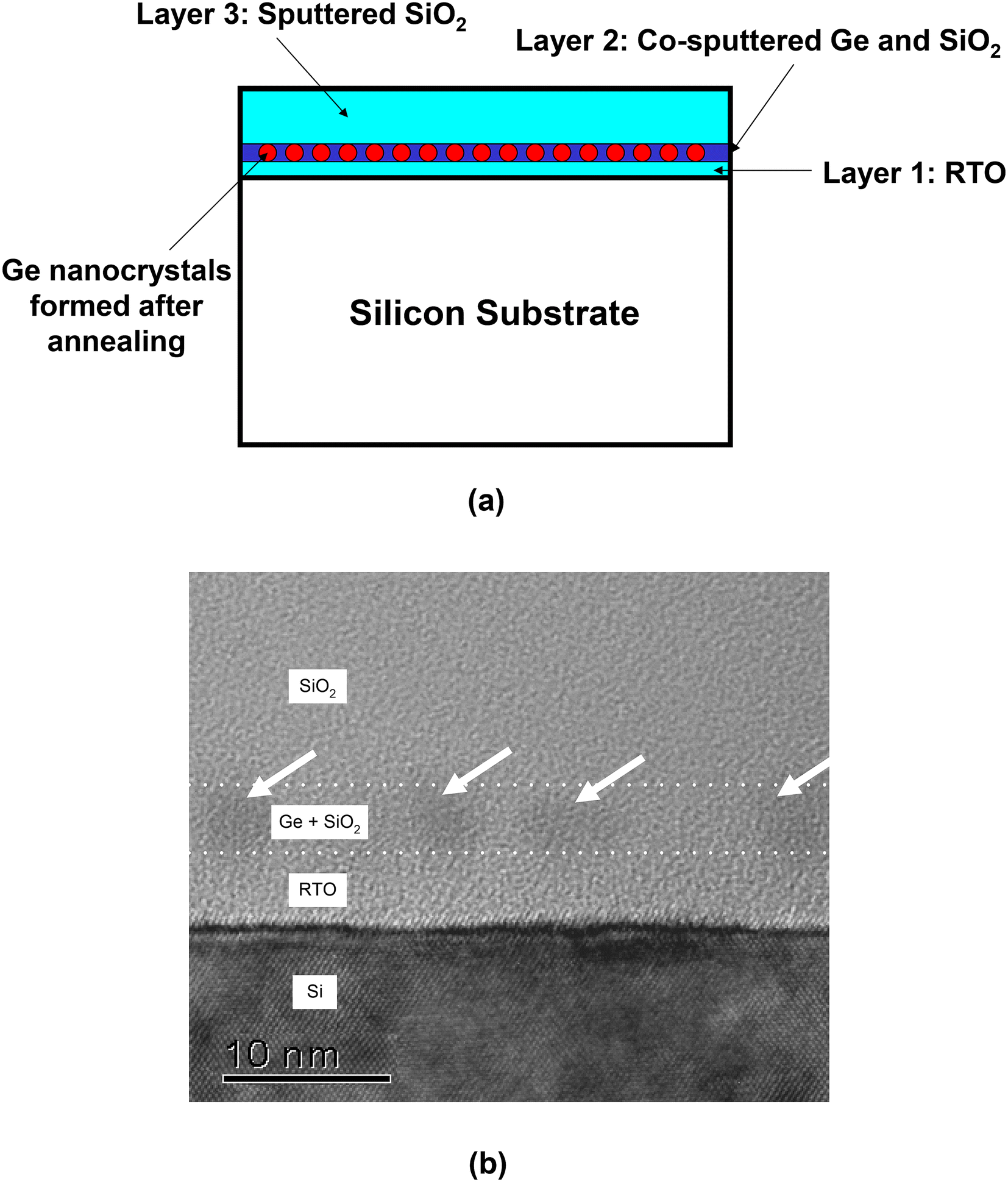 | ||
| Fig. 1 (a) Schematic diagram of the tri-layer insulator gate stack structure. (b) TEM cross-section showing the formation of germanium nanocrystals (indicated by white arrows) in a 3 nm thick middle layer (bound by dotted white lines) of the tri-layer insulator gate stack structure. (b) Reproduced with permission from ref. 70, Copyright 2002, AIP Publishing. | ||
Alternatively, the Ge nanocrystals can be formed by the wet oxidation of 10 nm-thick silicon–germanium Si0.54Ge0.46 films.74 The device fabrication sequence for this method can be described as follows. A tunnel oxide was grown on a (100)-oriented p-type Si substrate via rapid thermal oxidation at 1000 °C for 30 s in pure oxygen. A layer of the Si0.54Ge0.46 film was then deposited using the RF sputtering technique at room temperature in Ar gas at a pressure of 3.3 mTorr. A typical deposition rate of 4 Å s−1 was obtained with a RF power of 100 W. The tunnel oxide and Si0.54Ge0.46 film structure were then annealed at 800 °C for 6 hours in a pure N2 ambience to form a tunnel oxide–polycrystalline Si0.54Ge0.46 structure. The thickness and Ge content of the Si0.54Ge0.46 film were determined using a step profiler and the Rutherford backscattering technique, respectively. Wet oxidation of the Si0.54Ge0.46 film was then performed at 600 °C for different durations using a conventional furnace. The structure was then capped with RF-sputtered SiO2 to achieve a tri-layer (tunnel oxide/oxidized polycrystalline Si0.54Ge0.46/RF-sputtered SiO2) structure as shown in Fig. 2. Finally, the tri-layer structure was obtained by RTA in either pure N2, Ar or forming gas (90% N2 + 10% H2) ambience using a two-step (1000 °C for 300 s followed by 700 °C for 60 s) annealing process to form the Ge nanodots.
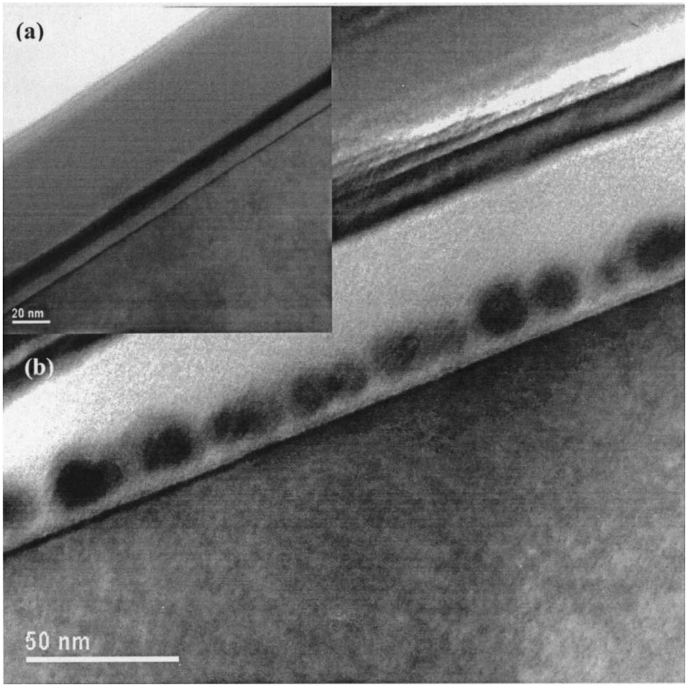 | ||
| Fig. 2 (a) Cross-section TEM micrograph of the Si0.54Ge0.46 film that has been wet oxidized at 600 °C for 60 min. (b) Cross-section TEM micrograph of the Ge nanodots formed by annealing the structure shown in (a) in N2 for 300 s at 1000 °C. Reproduced with permission from ref. 74, Copyright 2004, AIP Publishing. | ||
The tri-layer gate structure, Ge nanocrystal capacitor devices with a high dielectric constant material as the tunnel dielectric in our work, typically consists of a 4.8 nm thick, or smaller EOT, hafnium dioxide (HfO2) layer deposited on a (100) n-type Si substrate.73 A thin layer (4 nm thickness) of Ge was RF sputter-deposited (at an operating pressure of 3.3 × 10⁻³ Torr and a power of 50 W) over the HfO2 tunnel dielectric film to form the middle sandwiched layer. This was then followed by the deposition of a cap oxide layer of 50 nm thickness. Subsequently, the structure was subjected to RTA at 1000 °C for 300 s in either nitrogen (N2) or argon (Ar) ambience to fabricate the Ge nanocrystals (see Fig. 1(a)) in the middle layer.69,70,72,73 The outer cap oxide layer was deposited by sputter deposition from a 99.999% pure silicon dioxide (SiO2) target. A sufficiently thick cap oxide layer of ∼40–50 nm thickness was selected to make sure that the out-diffusion of Ge was minimized during the high temperature RTA step, therefore preserving the charge storage performance of the memory device. For fabricating the tunnel dielectric stack with a smaller EOT of 1.9 nm in the Ge nanocrystal capacitor devices, surface nitridation was first carried out at 700 °C for 1 minute (min) in an ammonia (NH3) ambience on a (100) n-type Si substrate to form a thin silicon oxynitride (SiOxNy) layer. This was followed by metal–organic chemical vapour deposition (MOCVD) at a temperature of 400 °C, using Hf(OC(CH3)3)4 as a precursor material with Ar carrier gas, to form the HfO2 layer. The various Ge nanocrystal capacitor device structures described in this work and the annealing ambience used in the synthesis of the Ge nanocrystals are summarised in Table 1.
|
3.3. Fabrication of germanium nanocrystal transistor structures
For characterizing the energy location of the traps in the Ge nanocrystals and studies on charge retention, n-channel MOSFET (nMOSFET) structures with either a silicon dioxide or hafnium aluminium oxide (HfAlO) tunnel dielectric layer were fabricated. The tri-layer stack for the nMOSFET devices with silicon dioxide as the tunnel dielectric typically consisted of a 5 nm thick tunnel oxide, a 5 nm thick middle layer with Ge nanocrystals and a cap oxide layer of 40 nm thickness.73 The fabrication process for the nMOSFET devices with HfAlO as the tunnel dielectric was reported previously73 and is described as follows. A tunnel dielectric stack, consisting of silicon oxynitride (SiOxNy) and HfAlO of 1 nm and 4 nm thickness respectively, was formed by surface nitridation at 700 °C for 1 min in an NH3 ambience on (100) p-type Si substrates, followed by the deposition at 450 °C of the HfAlO film with a deposition source of HfAl(MMP)2(OiPr)5. Post-deposition annealing was subsequently carried out for 1 min at 700 °C in a N2 ambience. The resulting tunnel dielectric gate stack has a measured EOT of ∼2 nm. Sputter deposition (at an operating pressure of 0.3 kPa and an RF power of 100 W) of a thin layer of Ge (∼4 nm thickness) was performed on the 2 nm EOT tunnel dielectric stack. This was then followed by the sputter deposition of a cap oxide layer of ∼20 nm thickness. The tri-layer gate structure was then subjected to RTA for a duration of 300 s at 1000 °C to form the Ge nanocrystals in the sandwiched layer. A tantalum nitride (TaN) film of ∼150 nm thickness was deposited to form the gate electrode layer by dc sputter deposition from a Ta target in an ambience consisting of a mixture of Ar and N2. Photolithography was then performed to pattern the gate electrode, followed by plasma etching. N+ source/drain implantation, with an arsenic ion (As+) dose of 1015 cm−2, at an energy of 100 keV and a 7° tilt angle was carried out. Finally, source/drain activation annealing at 950 °C for 30 s was performed. Fig. 3(a) and (b) show the fabrication process flow schematic and the TEM cross-section of the Ge nanocrystal memory transistor, respectively.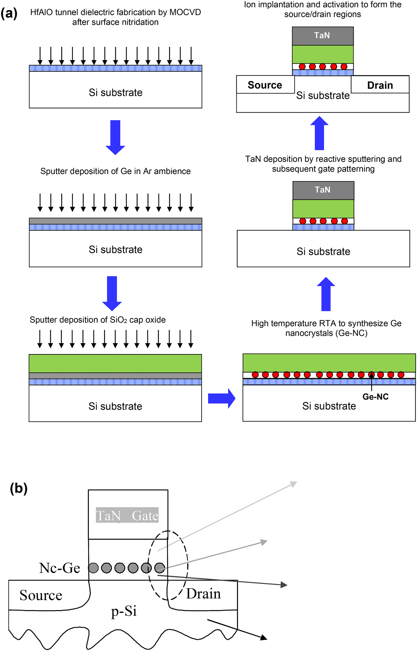 | ||
| Fig. 3 (a) Schematic diagram of the fabrication process flow of the Ge nanocrystal memory transistor. (b) Schematic and TEM cross-section of the Ge nanocrystal memory transistor showing the Ge nanocrystals formed in the middle layer of the tri-layer gate structure. (a) Reproduced with permission from ref. 73, Copyright 2023, American Chemical Society. | ||
4. Charge storage, mechanism and characterization
4.1. Verification of the charge storage capability of Ge nanocrystals in the tri-layer gate structure
We first tested the fabricated Ge nanocrystal tri-layer gate structure capacitors using high frequency capacitance–voltage (C–V) measurements for charge storage. To verify that the anti-clockwise C–V hysteresis, indicating charge storage, is due to the presence of Ge nanocrystals, we compared two types of tri-layer gate structure devices on a p-type Si substrate. Both device A and B are tri-layer gate structures with a 5 nm thick silicon dioxide as the tunnel dielectric and a 50 nm thick silicon oxide as the cap layer. The middle layer (which is sandwiched between the tunnel dielectric and the cap oxide layer) is a 20 nm thick layer of co-sputtered Ge and silicon oxide for device A and only a 20 nm thick layer of sputtered silicon oxide (without Ge) for the control device B. Germanium nanocrystals are formed in device A after rapid thermal annealing at 1000 °C for 300 s in an argon ambience, which is confirmed using transmission electron microscopy (TEM) as shown in Fig. 4(a). The measured high-frequency C–V characteristics of both devices A and B are shown in Fig. 4(b). It is observed that there is negligible hysteresis in the C–V characteristics of control device B (without Ge nanocrystals), as compared to device A with Ge nanocrystals. This suggests that Ge nanocrystals are responsible for the C–V hysteresis and charge storage.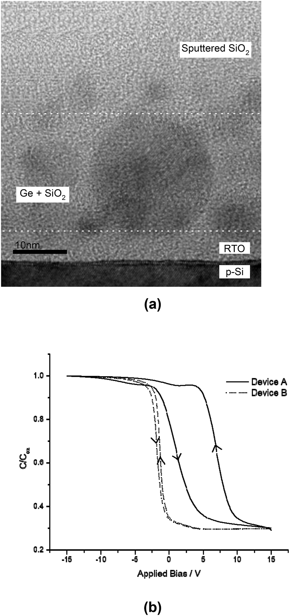 | ||
| Fig. 4 (a) TEM cross-section showing the formation of germanium nanocrystals in a 20 nm thick middle layer (bound by dotted white lines) of the tri-layer insulator gate stack structure. (b) Anti-clockwise hysteresis in the high frequency C–V characteristics of device A (with Ge nanocrystals) indicating the charge storage or memory effect as compared to the negligible hysteresis in control device B (without Ge nanocrystals). Adapted with permission from ref. 69, Copyright 2002, AIP Publishing. | ||
4.2. Influence of the middle layer thickness in the tri-layer gate structure on charge storage
We investigated the effect of the middle layer (Ge plus silicon oxide) thickness on the charge storage performance of the tri-layer gate structure capacitor devices. Devices A, D and E have different middle layer thicknesses of 20 nm, 6 nm and 3 nm respectively, but with a similar tunnel oxide thickness of 5 nm and a similar cap oxide thickness of 50 nm. We found that a smaller middle layer thickness results in greater charge storage due to the increase in nanocrystal density as demonstrated in Fig. 5(a) and (b) for devices D and E, respectively. The high frequency C–V characteristics and the charge storage performances (extracted from the size of the C–V hysteresis loops) of devices A, D and E are shown in Fig. 6(a) and (b) respectively.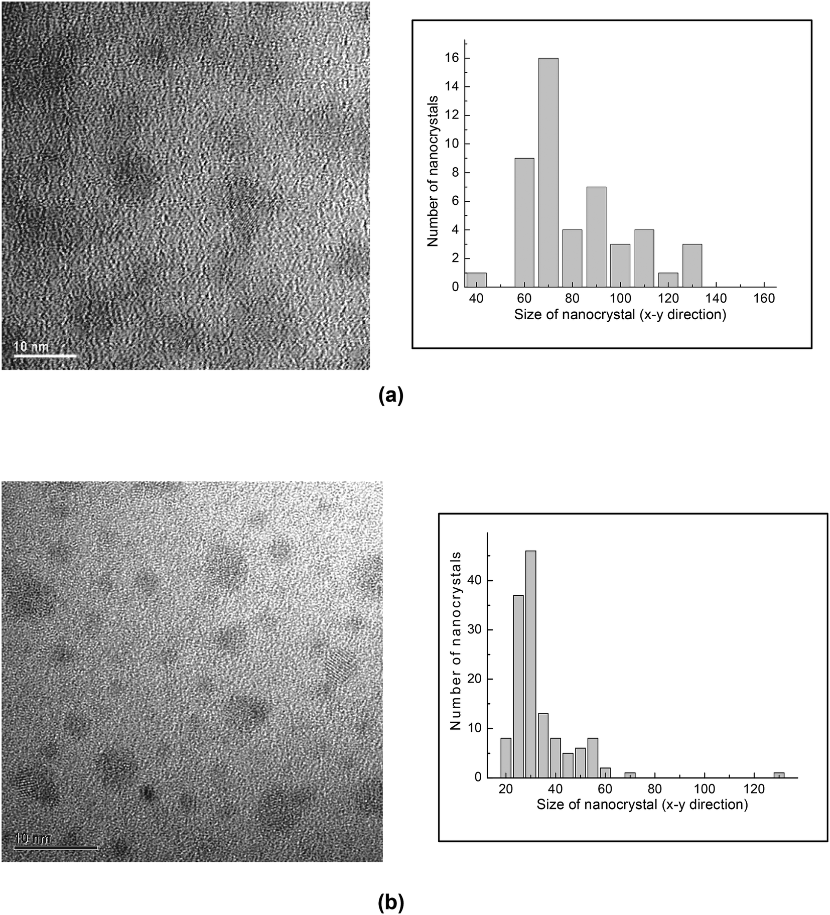 | ||
| Fig. 5 (a) Planar TEM image and size distribution histogram of the Ge nanocrystals of a trilayer structure consisting of 5 nm of tunnel oxide and 50 nm cap oxide with (a) a 6 nm thick middle layer (device D) and (b) a 3 nm thick middle layer (device E). Adapted with permission from ref. 70, Copyright 2002, AIP Publishing. | ||
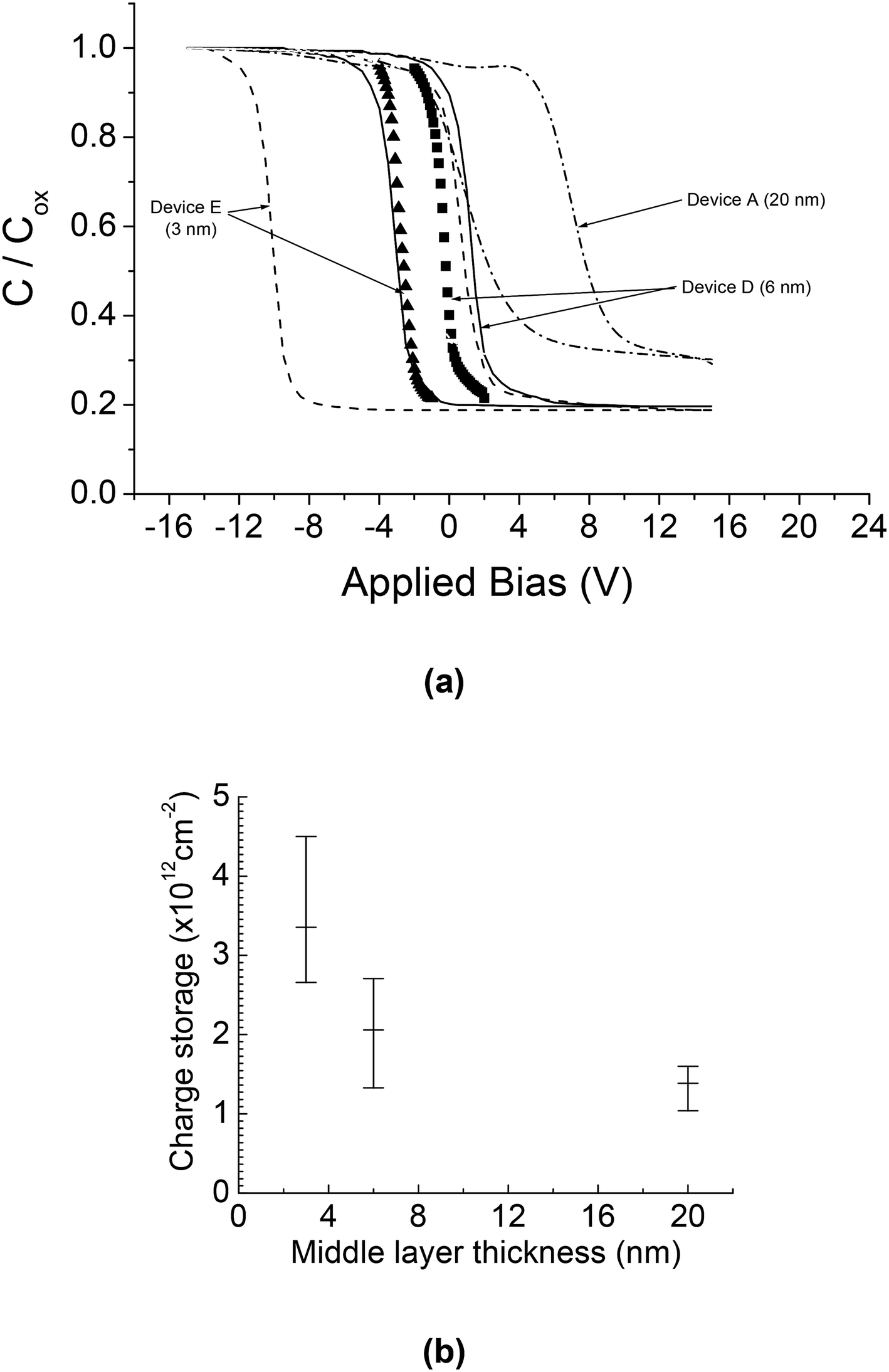 | ||
| Fig. 6 (a) High-frequency C–V characteristics of devices A, D and E having different middle layer thicknesses of 20 nm, 6 nm and 3 nm, respectively, but with a similar tunnel oxide thickness of 5 nm and a similar cap oxide thickness of 50 nm. The quasi-neutral C–V curves for devices D and E (solid squares and triangles respectively) were obtained by restricting the gate bias to a very narrow range to minimize charging up of the Ge nanocrystals. (b) Charge storage performance (extracted from the size of the C–V hysteresis loop) of devices A, D and E. Adapted with permission from ref. 70, Copyright 2002, AIP Publishing. | ||
4.3. Charge storage mechanism in germanium nanocrystals
Both Ar and forming gas were employed in the investigation on the effect of different gas ambiences used during the high temperature RTA annealing on the charge storage performance of the tri-layer gate structure Ge nanocrystal capacitors with a tunnel oxide thickness of 5 nm, a middle layer thickness of 3 nm and a cap oxide thickness of 50 nm (devices E and F). It was observed that after annealing in forming gas (with 10% hydrogen) at 1000 °C for 300 s, the C–V hysteresis disappeared (device F), as compared to Ar annealing (device E) where the C–V hysteresis loop still remains after the annealing step as shown in Fig. 7(a). The planar TEM micrographs of the middle layer of devices E and F annealed in the two different gas ambiences, as shown in Fig. 7(b) and (c) respectively, were also analyzed. There was no observable difference in the morphology of the synthesized Ge nanocrystals after annealing in the two different gas ambiences. This suggested that the disappearance of the hysteresis after forming gas annealing was neither due to the lack of formation of Ge nanocrystals nor a morphological difference in the synthesized Ge nanocrystals. Alternatively, it is possible that hydrogen passivation could also increase Ge diffusion and thus degrade the tunnel oxide, but this is somewhat difficult to ascertain. | ||
| Fig. 7 (a) High-frequency C–V characteristics of nanocrystal capacitors with a tunnel oxide thickness of 5 nm, a middle layer thickness of 3 nm and a cap oxide thickness of 50 nm after annealing in argon (Ar) (device E) and forming gas (device F). Device F that was annealed in forming gas showed negligible C–V hysteresis (or charge storage) as compared to device E annealed in Ar. (b) and (c) Planar TEM images of Ge nanocrystals of trilayer structures consisting of 5 nm tunnel oxide, a 3 nm middle layer and 50 nm cap oxide after annealing in argon (device E) and forming gas (device F). | ||
Lower temperature annealing at 450 °C in a hydrogen-rich ambience was also conducted on devices that exhibited C–V hysteresis. It was observed that for devices which initially exhibited the C–V hysteresis or memory effect, the hysteresis was still present, although this had decreased a little, after low temperature annealing in forming gas. The result therefore suggested that trap sites within the Ge nanocrystals store charges. For the complete passivation of these trap sites, high temperature annealing in a hydrogen-rich ambience was required.
Similar observations as mentioned above were also found in the Ge nanocrystals synthesized by the wet oxidation of 10 nm-thick Si0.54Ge0.46 films.74 In our previous study in ref. 74, it was suggested that it was unlikely that charges were stored in the conduction band of the Ge nanocrystals or at bulk oxide defects. The charge storage mechanism was closely related to the reduction of Si–O–Ge bonds by hydrogen (H) species. The Si–O–Ge bonds were most likely to be located at the outer surface of the Ge nanocrystals where the Ge atoms form bonds with the silicon oxide matrix. It was possible that during RTA at 1000 °C in a forming gas ambience, H species can reduce GeOx (i.e., Si–O–Ge bonds) and subsequently passivate the Ge dangling bonds at the interface of the Ge nanocrystals. Upon annealing at a low temperature of 450 °C in forming gas, the H atoms were prevented from passivating the trap sites by the thin layer of mixed oxides (i.e., Si–O–Ge) enfolding the core of the Ge nanocrystals. Hence, the charge storage mechanism for the tri-layer gate structures is closely related to the interfacial traps of the Ge nanocrystals.
The C–V characteristics of capacitor tri-layer gate structures, embedded with Ge nanocrystals and a silicon dioxide tunnel dielectric, are shown in Fig. 8(a) and (b) for p-type and n-type Si substrates, respectively. The C–V characteristics show evidence of both electron and hole trapping in the Ge nanocrystals. Charge separation experiments on Ge nanocrystal transistor structures (not shown) provided further evidence of hole trapping in the Ge nanocrystals. Table 2 shows the extracted charge storage density (from C–V hysteresis) and nanocrystal density (from planar TEM analysis) for devices D, E and G having different middle layer thicknesses of 6 nm, 3 nm and 4 nm respectively, but with a similar tunnel oxide thickness of 5 nm and a similar cap oxide thickness of 50 nm. The charge storage density Nnc (in units of cm−2) was estimated from the C–V hysteresis based on the following equation:
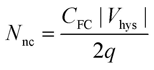 | (1) |
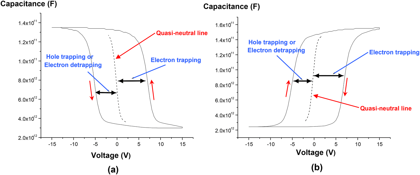 | ||
| Fig. 8 High-frequency C–V characteristics of capacitor tri-layer gate structures embedded with Ge nanocrystals and a silicon dioxide tunnel dielectric for (a) p-type and (b) n-type (100) Si substrates. Reproduced with permission from ref. 73, Copyright 2023, American Chemical Society. | ||
| Device | Charge storage from C–V hysteresis (cm−2) | Nanocrystal density (cm−2) |
|---|---|---|
| D (6 nm ML) | 7.5 × 10¹¹ | 5.7 × 10¹¹ |
| E (3 nm ML) | 2.2 × 10¹² | 1.6 × 10¹² |
| G (4 nm ML) | 1.2 × 10¹² | 9.1 × 10¹¹ |
We have also employed scanning capacitance spectroscopy/microscopy (SCS/SCM), a scanning probe microscope-based nano-characterization method, for analyzing the hole and electron charging of Ge nanodot structures. Fig. 9 shows a Ge nanodot array that was deposited on a highly doped p-type Si substrate with an anodic alumina mask.75 The SCM differential capacitance (dC/dV) profile in Fig. 9 shows a negative peak before forming gas annealing. This suggests that the Ge nanodots exhibit hole trapping characteristics, and contrast reversal effects, during the SCM characterization.75 After annealing in forming gas at a relatively low temperature of 450 °C, the disappearance of the dC/dV negative characteristic peak suggests that the hole traps have been completely passivated by the hydrogen species in the forming gas. This experiment, using SCS/SCM characterization, demonstrated charge storage by hole traps in the Ge nanodots and subsequent passivation of these traps by hydrogen species after forming gas annealing. After the low temperature forming gas annealing, partial passivation of electron traps, as compared to the complete passivation of hole traps, was also observed. Based on this observation, we therefore suggested that hole traps were located close to, or at, the surfaces of the Ge nanodots as compared to electron trap sites that could possibly be situated deeper within the Ge nanodots. Further explanation regarding the hole and electron trapping in Ge nanodots and passivation of the traps is given in ref. 75.
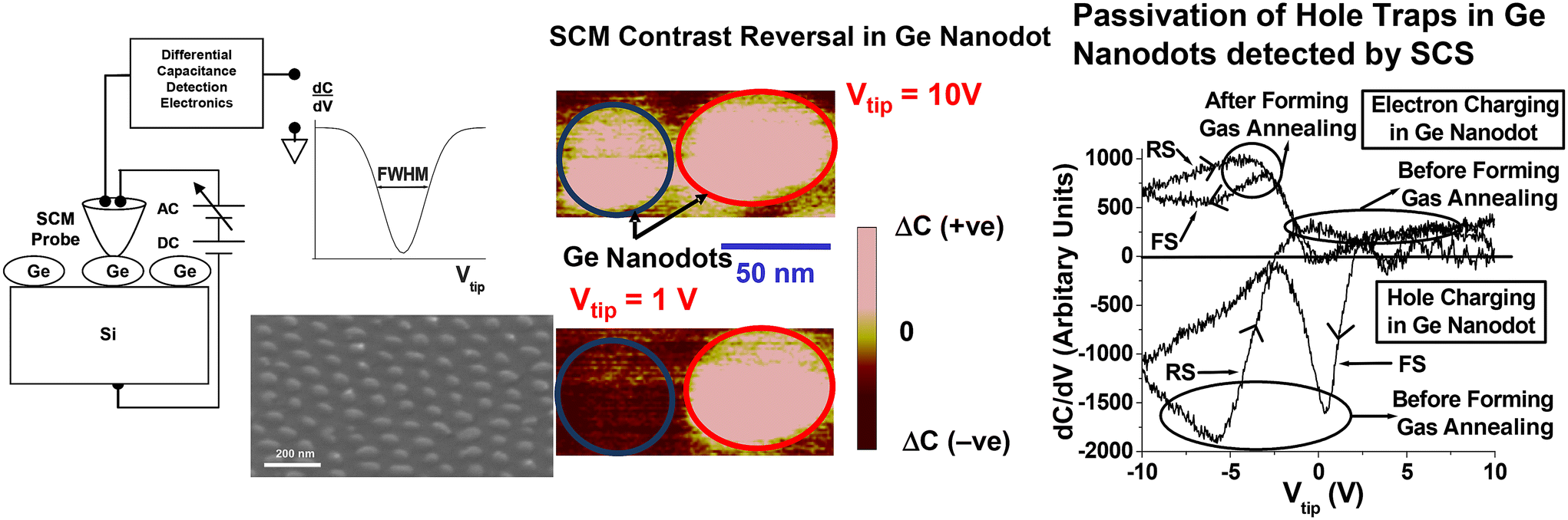 | ||
| Fig. 9 Scanning capacitance spectroscopy/microscopy (SCS/SCM) of Ge nanodots before and after forming gas annealing at 450 °C showing electron and hole charging in Ge nanodots. Reproduced with permission from ref. 75, Copyright 2008, AIP Publishing. | ||
4.4. Use of high dielectric constant materials in the tri-layer gate structure
A thin tunnel oxide in the tri-layer gate structure Ge nanocrystal memory device is desirable as this results in lower program and erase voltages during operation. However, significant penetration of Ge through the tunnel oxide layer into the silicon substrate was observed for devices with a tunnel oxide thickness of 2.5 nm (device RTO2-5) after the synthesis process as shown in Fig. 10(a). The cross-sectional high-resolution transmission electron microscopy (HRTEM) micrograph of device RTO2-5 in Fig. 10(a) shows that the lack of Ge nanocrystal formation was possibly due to the diffusion and penetration of Ge through the 2.5 nm thick SiO2 tunnel dielectric layer during the 1000 °C RTA process.72,73 The oxide–Si interface seemed rather uneven and the original Ge middle sandwiched layer had also disappeared after the high temperature RTA process. The uneven oxide–Si interface was likely a result of significant Ge diffusion from the sandwiched layer into the Si substrate. As a result of the high concentration gradient of Ge between the sandwiched layer and the Si substrate, together with the thin silicon dioxide diffusion barrier, it was highly probable that Ge had penetrated into the Si substrate after the high temperature RTA step. Consequently, hardly any Ge nanocrystals were formed in the middle sandwiched layer of the tri-layer gate structure. The absence of nanocrystal formation would result in the inability of the tri-layer gate structure to store charge, as evidenced from the lack of a significant hysteresis in the C–V characteristics. As a solution to this issue, we investigated the use of high dielectric constant (high-κ) materials to replace the silicon dioxide tunnel oxide in the tri-layer gate structure. Fig. 10(b) presents a HRTEM image showing evidence of Ge nanocrystal formation in device HK1-9 consisting of a HfO2/SiOxNy tunnel dielectric stack with an EOT of 1.9 nm.72,73 The larger physical thickness (∼7 nm) of the HfO2/SiOxNy tunnel dielectric stack seemed to be effective in minimizing Ge penetration, although device HK1-9 has a smaller EOT than device RTO2-5. The ability of the high-κ material to prevent significant Ge diffusion into the Si substrate was further confirmed by the SIMS results for device HK1-9 in Fig. 10(c), which shows that there was still significant Ge remaining in the Ge middle layer after the 1000 °C RTA step.73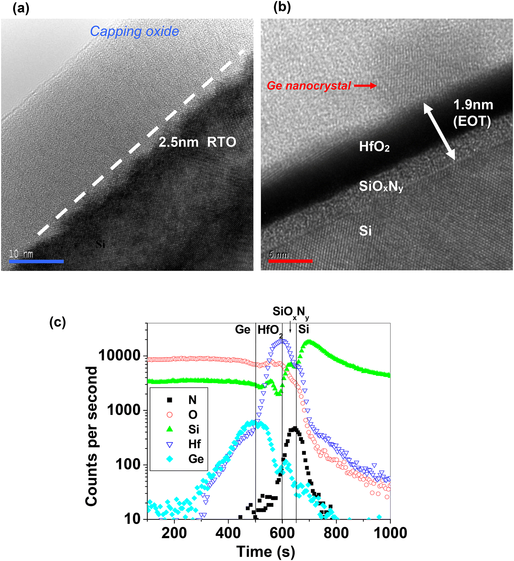 | ||
| Fig. 10 HRTEM cross-sectional micrographs of (a) device RTO2-5 and (b) device HK1-9. Notable absence of Ge nanocrystals and the uneven oxide–Si interface, resulting from Ge penetration, in device RTO2-5 was observed. The horizontal blue and red scale markers in (a) and (b) represent 10 nm and 5 nm, respectively. Reproduced with permission from ref. 72, Copyright 2004, AIP Publishing. (c) Secondary ion mass spectroscopy (SIMS) depth profile of device HK1-9. Germanium did not penetrate significantly into the Si substrate after the 1000 °C RTA step. The HfO2/SiOxNy dielectric stack layer provided an effective barrier in the synthesis of Ge nanocrystals. Reproduced with permission from ref. 73, Copyright 2023, American Chemical Society. | ||
4.5. Germanium nanocrystal transistor characterization and trap energy
We also experimented with Ge nanocrystal transistor structures to investigate whether the trap energy can be modulated by changing the tunnel dielectric material to provide a longer charge retention duration. This is motivated by our postulation that the trap storage sites could be located at the surfaces of the Ge nanocrystals that were in direct contact with the tunnel dielectric. Germanium nanocrystal nMOSFET transistor structures, with 10 μm and 100 μm gate length and width, respectively, and with hafnium aluminium oxide (HfAlO) as the tunnel dielectric, were used for the trap characterization studies. The Ge nanocrystal nMOSFETs were first charged up using an 8 V, 60 s write (program) pulse. Subsequently, the discharge of the stored electrons in the nanocrystal transistors was noted by observing the drain current transients at a smaller voltage of 4 V at different temperatures of 25 °C–200 °C in steps of 25 °C or 50 °C. Fig. 11(a) shows that as the electrons were progressively being emitted from the nanocrystal trap sites, the drain current increased.73 The duration for the drain current transient to reach saturation, or the discharge duration of the stored electrons, was noted. The electron discharge duration (τe) was noted for different temperatures (T). The inverse of the products of τe and T2 was plotted against 1000/T (i.e., Arrhenius plot). The plot is based on the following equation: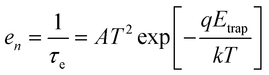 | (2) |
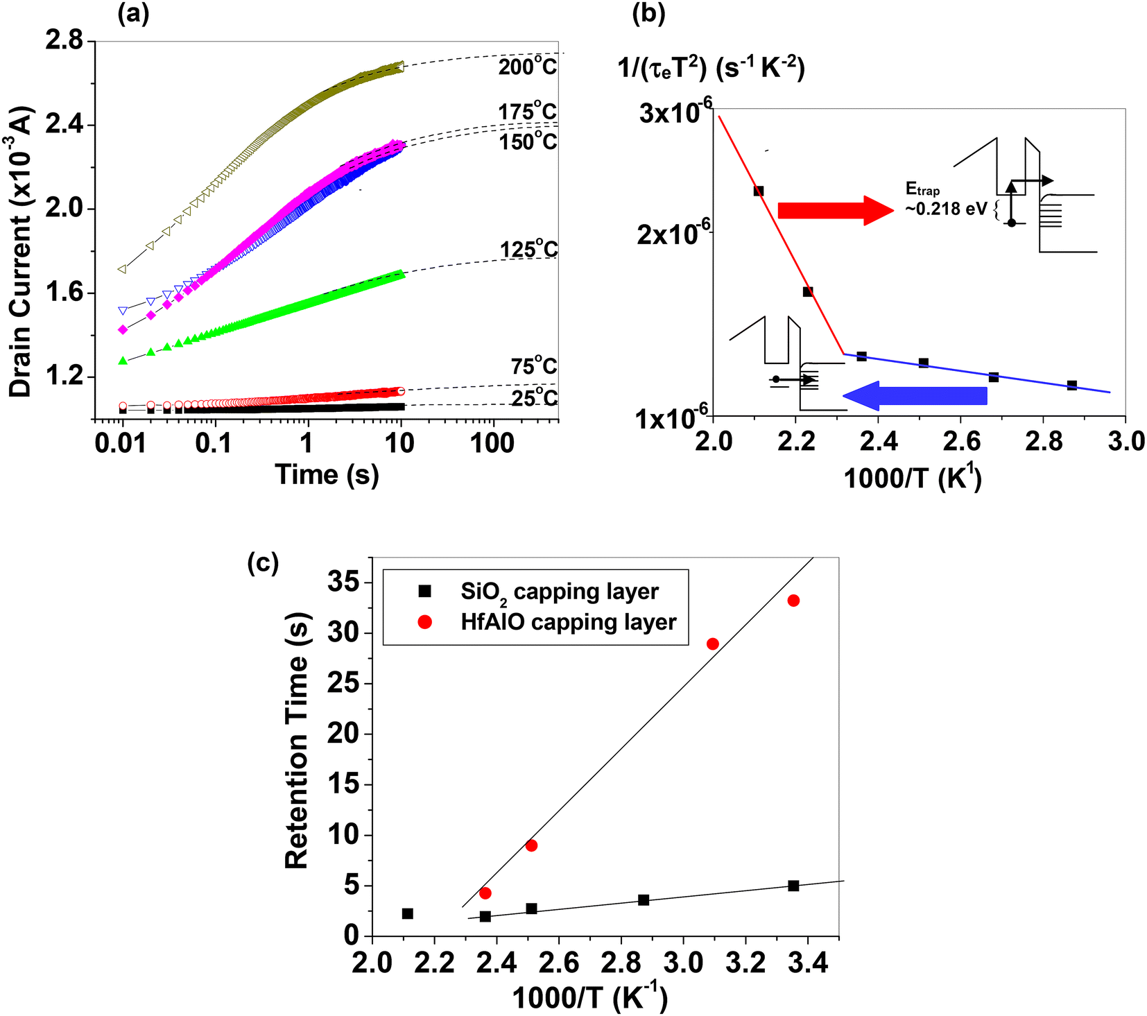 | ||
| Fig. 11 (a) Drain current transients at a gate bias of 4 V following a write operation at 8 V for 60 s for the tri-layer gate structure Ge nanocrystal transistor (HfAlO as the tunnel dielectric material). Dashed lines are fitted simulation results to the measurement data (symbols). (b) Arrhenius plot of the inverse of the products of τe and T2versus 1000/T, where τe and T are the electron discharge time and temperature, respectively. (c) Temperature dependence of retention time for tri-layer gate structure Ge nanocrystal capacitors with SiO2 and HfAlO cap layers. Reproduced with permission from ref. 73, Copyright 2023, American Chemical Society. | ||
The tunnel oxide thickness affects the program (or charging) performance and the charge retention performance of a memory device. A thinner tunnel oxide thickness will allow the use of a smaller charging voltage and/or a charging pulse with a shorter duration, thus increasing the program efficiency of the memory cell. However, a too small tunnel oxide thickness can compromise the charge retention performance of the Ge nanocrystal memory device, as the trapped (or stored) charge carriers can tunnel easily through the thin tunnel oxide back into the Si substrate. Hence, a compromise has to be sought in the selection of a suitable tunnel oxide thickness to balance program efficiency with the charge retention performance of the Ge nanocrystal memory device. Tunnelling and capture processes take place during the charging process of the Ge nanocrystals while tunnelling and possibly detrapping (depending on the temperature) are involved during the discharge process of the Ge nanocrystals. Charges trapped in the conduction band of Ge nanocrystals generally show a shorter retention time than those trapped in the defect states within the Ge nanocrystal bandgap. The non-uniformity of the Ge nanocrystals could affect the tunnelling distance of the trapped charge carriers and this could impact the discharge duration or charge retention time.
We also carried out studies to investigate whether the trap energy could be modulated by replacing the cap oxide material in the tri-layer gate structure. Fig. 11(c) shows that capacitors with the HfAlO cap oxide exhibited a greater temperature dependence of the charge retention duration, and also a longer charge retention duration, as compared to devices with a similar tri-layer gate structure but with SiO2 as the cap oxide. The results therefore suggested that deeper trap levels were generated at the nanocrystal–Ge/HfAlO interface as compared to those at the nanocrystal–Ge/SiO2 interface. It should be noted that the short retention time of the devices, as observed in Fig. 11(c), is based on charge retention experiments conducted on capacitor test structures, with the retention time defined arbitrarily as the time taken for the capacitance transient to decrease to a normalized capacitance value of 0.5 after the capacitor has been initially charged up. The retention times in Fig. 11(c) are to be interpreted on a comparative basis to show the effect of different cap dielectric materials on the nanocrystal trap energy level and should not be used to compare in absolute value terms with those reported in the literature; the latter is based on transistor devices and typically extrapolated to years based on the operational conditions of the device.
5. Conclusions
In this review of Ge nanocrystal memory devices, fabrication techniques for synthesizing and controlling the size and distribution of Ge nanocrystals in a tri-layer insulator gate stack structure were presented. The memory or charge storage effect was observed and verified in the tri-layer gate Ge nanocrystal structures. Investigations into the charge storage mechanism and electrical performance of Ge nanocrystal memory devices were discussed. From the high temperature annealing experiments performed in argon (or nitrogen) and forming gas ambiences, we concluded that charge storage in the tri-layer gate structures was closely related to bulk/interfacial electron and hole traps within, or at the surface of, the Ge nanocrystals. The use of SCS/SCM to analyze carrier charging in Ge nanodots and the passivation of hole and electron traps after forming gas annealing was demonstrated and has led to a better understanding of the charge storage mechanism in the Ge nanodots or nanocrystals. From investigations on the Ge nanocrystal transistors, it was shown that the energy of the traps, responsible for nanocrystal charge storage, can be modulated by using different tunnel or cap dielectric materials. A deeper trap level results in a longer charge retention duration for the Ge nanocrystal transistor, and hence better charge retention performance, when used as a NVM device.It has been demonstrated that the charge retention performance of the nanocrystal memory transistor is largely dependent on the trap energy level in the nanocrystals. Future directions could include the possibility of introducing deep trap energy levels into the nanocrystal bandgap by doping with suitable materials. Possible candidate impurity materials are metals as these have work functions that are larger than the electron affinity of Ge. If the metal implanted in the Ge nanocrystals does not react with the surrounding material, it may create a trap energy level in the nanocrystalline Ge bandgap with a trap energy given by the difference between the Ge electron affinity and the work function of the metal. From predictions of the required trap energy for 10-years charge retention, metals such as Co, Au and Ni can satisfy the trap energy level requirement for Ge nanocrystals with diameters of 1–5 nm.78 However, the introduction of metallic impurities into the nanocrystal memory device may cause leakage and other process compatibility related issues.
Author contributions
W. K. Chim wrote the entire manuscript.Data availability
No primary research results, software or code have been included and no new data were generated or analysed as part of this review.Conflicts of interest
There are no conflicts to declare.Acknowledgements
I would like to acknowledge the contributions of my fellow co-workers, especially the late W. K. Choi, past PhD students, L. W. Teo, E. W. H. Kan, B. H. Koh, T. H. Ng and others, and former colleagues from the Singapore-MIT Alliance (SMA) program, D. A. Antoniadis and E. A. Fitzgerald. This work is dedicated to the memory of my former colleague, the late W. K. Choi.References
- J. V. Barth, G. Costantini and K. Kern, Nature, 2005, 437, 671–679 CrossRef CAS PubMed.
- S. Tiwari, F. Rana, K. Chan, H. Hanafi, W. Chan and D. Buchanan, Int. Electron Devices Meet., Tech. Dig., 1995, 521–524 CAS.
- L. Guo, E. Leobandung and S. Y. Chou, Appl. Phys. Lett., 1997, 70, 850–852 CrossRef CAS.
- A. Nakajima, T. Futatsugi, K. Kosemura, T. Fukano and N. Yokoyama, Appl. Phys. Lett., 1997, 70, 1742–1744 CrossRef CAS.
- J. J. Lee and D. L. Kwong, IEEE Trans. Electron Devices, 2005, 52, 507–511 CrossRef.
- Y. H. Lin, C. H. Chien, C. T. Lin, C. W. Chen, C. Y. Chang and T. F. Lei, Int. Electron Devices Meet., Tech. Dig., 2004, 1080–1082 CAS.
- Y. H. Lin, C. H. Chien, C. T. Lin, C. Y. Chang and T. F. Lei, IEEE Electron Device Lett., 2005, 26, 154–156 CAS.
- H. Silva, M. K. Kim, A. Kumar, U. Avci and S. Tiwari, Int. Electron Devices Meet., Tech. Dig., 2003, 271–274 CAS.
- L. Guo, E. Leobandung and S. Y. Chou, Science, 1997, 275, 649–651 CrossRef CAS PubMed.
- C. Busseret, S. Ferraton, L. Montes and J. Zimmermann, IEEE Trans. Electron Devices, 2006, 53, 14–22 CAS.
- S. Tiwari, F. Rana, H. Hanafi, A. Hartstein, E. F. Crabbe and K. Chan, Appl. Phys. Lett., 1996, 68, 1377–1379 CrossRef CAS.
- J. J. Welser, S. Tiwari, S. Rishton, K. Y. Lee and Y. Lee, IEEE Electron Device Lett., 1997, 18, 278–280 Search PubMed.
- Y. C. King, T. J. King and C. Hu, Int. Electron Devices Meet., Tech. Dig., 1998, 115–118 CAS.
- Z. Liu, C. Lee, V. Narayanan, G. Pei and E. C. Kan, IEEE Trans. Electron Devices, 2002, 49, 1606–1613 CrossRef CAS.
- Z. Liu, C. Lee, V. Narayanan, G. Pei and E. C. Kan, IEEE Trans. Electron Devices, 2002, 49, 1614–1622 CrossRef CAS.
- A. Nakajima, T. Futatsugi, N. Horiguchi, H. Nakao and N. Yokoyama, Int. Electron Devices Meet., Tech. Dig., 1997, 159–162 CAS.
- D. Kahng and S. M. Sze, Bell Syst. Tech. J., 1967, 46, 1288–1295 CrossRef.
- D. Frohman-Bentchkowsky, IEEE J. Solid-State Circuits, 1971, sc-6, 301–306 Search PubMed.
- P. C. Y. Chen, IEEE Trans. Electron Devices, 1977, 24, 584–586 Search PubMed.
- W. Johnson, G. Perlegos, A. Renninger, G. Kuhn and T. Ranganath, IEEE Int. Solid-State Circuits Conf. Tech. Dig., 1980, 152–153 Search PubMed.
- F. Masuoka, M. Asano, H. Iwahashi, T. Komuro and S. Tanaka, Int. Electron Devices Meet., Tech. Dig., 1984, 464–467 Search PubMed.
- Y. Shi, K. Saito, H. Ishikuro and T. Hiramato, J. Appl. Phys., 1998, 84, 2358–2360 CrossRef CAS.
- R. Thielsch and H. Bottcher, Chem. Phys. Lett., 1992, 189, 226–230 CrossRef CAS.
- C. R. Stoldt, M. A. Haag and B. A. Larsen, Appl. Phys. Lett., 2008, 93, 43125 CrossRef.
- M. Nogami and Y. Abe, Appl. Phys. Lett., 1994, 65, 2545–2547 CrossRef CAS.
- I. E. Tyschenko, V. A. Volodin, L. Rebohe, M. Voelskov and V. Skorupa, Semiconductors, 1999, 33, 523–528 CrossRef CAS.
- K. M. Hassan, A. K. Sharma, J. Narayan, J. F. Muth, C. W. Teng and R. M. Kolbas, Appl. Phys. Lett., 1999, 75, 1222–1224 CrossRef CAS.
- S. Ngiam, K. F. Jensen and K. D. Kolenbrander, J. Appl. Phys., 1994, 76, 8201–8203 CrossRef CAS.
- A. Kanjilal, J. L. Hansen, P. Gaiduk and A. N. Larsen, Appl. Phys. Lett., 2003, 82, 1212–1214 CrossRef CAS.
- M. Kanoun, M. Lemiti, G. Bremond, A. Souifi, E. Bassani and I. Berbezier, Superlattices Microstruct., 2004, 36, 143–148 CrossRef CAS.
- A. Karmous, A. Cuenat, A. Ronda, I. Berbezier, S. Atha and R. Hull, Appl. Phys. Lett., 2004, 85, 6401–6403 CrossRef CAS.
- D. Szkutnik, A. Karmous, F. Bassani, A. Ronda, I. Berbezier, K. Gacem, A. El Hdiy and M. Troyon, Eur. Phys. J.: Appl. Phys., 2008, 41, 103–106 CrossRef.
- T. Stoica and E. Sutter, Nanotechnology, 2006, 17, 4912–4916 CrossRef CAS.
- B. R. Taylor, S. M. Kauzlarich, H. W. H. Lee and G.R. Delgado, Chem. Mater., 1998, 10, 22–24 CrossRef CAS.
- B. R. Taylor, S. M. Kauzlarich, G. R. Delgado and H. W. H. Lee, Chem. Mater., 1999, 11, 2493–2500 CrossRef CAS.
- R. S. Tanke, S. M. Kauzlarich, T. E. Patten, K. A. Pettigrew, D. L. Murphy, M. E. Thompson and H. W. H. Lee, Chem. Mater., 2003, 15, 1682–1689 CrossRef CAS.
- A. J. Pugsley, C. L. Bull, A. Sella, G. Sankar and P. F. McMillan, J. Solid State Chem., 2011, 184, 2345–2352 CrossRef CAS.
- X. Ma, F. Wu and S. M. Kauzlarich, J. Solid State Chem., 2008, 181, 1628–1633 CrossRef CAS.
- J. R. Heath, J. J. Shiang and A. P. Alivisatos, J. Chem. Phys., 1994, 101, 1607–1615 CrossRef CAS.
- E. J. Henderson, C. M. Hessel and J. G. C. Veinot, J. Am. Chem. Soc., 2008, 130, 3624–3632 CrossRef CAS PubMed.
- D. Gerion, N. Zaitseva, C. Saw, M. F. Casula, S. Fakra, T. V. Buuren and G. Galli, Nano Lett., 2004, 4, 597–602 CrossRef CAS.
- H. P. Wu, J. F. Liu, Y. W. Wang, Y. W. Zeng and J. Z. Jiang, Mater. Lett., 2006, 60, 986–989 CrossRef CAS.
- E. Fok, M. Shih, A. Meldrum and J. G. C. Veinot, Chem. Commun., 2004, 386–387 RSC.
- S. Prabakar, A. Shiohara, S. Hanada, K. Fujioka, K. Yamamoto and R.D. Tilley, Chem. Mater., 2010, 22, 482–486 CrossRef CAS.
- J. H. Warner and R. D. Tilley, Nanotechnology, 2006, 17, 3745–3749 CrossRef CAS.
- H. W. Chiu and S. M. Kauzlarich, Chem. Mater., 2006, 18, 1023–1028 CrossRef CAS.
- S. C. Codoluto, W. J. Baumgardner and T. Hanrath, CrystEngComm, 2010, 12, 2903–2909 RSC.
- D. A. Ruddy, J. C. Johnson, E. R. Smith and N. R. Neale, ACS Nano, 2010, 4, 7459–7466 CrossRef CAS PubMed.
- J. Wu, Y. Sun, R. Zou, G. Song, Z. Chen, C. Wang and J. Hu, CrystEngComm, 2011, 13, 3674–3677 RSC.
- D. Carolan and H. Doyle, J. Mater. Chem. C, 2014, 2, 3562–3568 RSC.
- T. K. Purkait, A. K. Swarnakar, G.B. De Los Reyes, F. A. Hegmann, E. Rivard and J. G. C. Veinot, Nanoscale, 2015, 7, 2241–2244 RSC.
- J. G. Couillard and H. G. Craighead, J. Mater. Sci., 1998, 33, 5665–5669 CrossRef CAS.
- S. Guha, M. Wall and L. L. Chase, Nucl. Instrum. Methods Phys. Res., B, 1999, 147, 367–372 CrossRef CAS.
- Y. Maeda, N. Tsukamono, Y. Yazawa, Y. Kanemitsu and Y. Masumoto, Appl. Phys. Lett., 1991, 59, 3168–3171 CrossRef CAS.
- D. Om, A. Kuperman and G. A. Ozin, Adv. Mater., 1994, 6, 147–150 CrossRef.
- L. Vescan and T. Stoica, J. Appl. Phys., 2002, 91, 10119–10126 CrossRef CAS.
- C. Palade, A. Slav, A. M. Lepadatu, A. V. Maraloiu, I. Dascalescu, S. Iftimie, S. Lazanu, M. L. Ciurea and T. Stoica, Appl. Phys. Lett., 2018, 113, 213106 CrossRef.
- C. Palade, A. Slav, A. M. Lepadatu, I. Stavarache, I. Dascalescu, A. V. Maraloiu, C. Negrila, C. Logofatu, T. Stoica, V. S. Teodorescu, M. L. Ciurea and S. Lazanu, Nanotechnology, 2019, 30, 445501 CrossRef CAS PubMed.
- C. Palade, A. M. Lepadatu, A. Slav, O. Cojocaru, A. Iuga, V. A. Maraloiu, A. Moldovan, M. Dinescu, V. S. Teodorescu, T. Stoica and M. L. Ciurea, J. Mater. Chem. C, 2021, 9, 12353–12366 RSC.
- I. Stavarache, O. Cojocaru, V. A. Maraloiu, V. S. Teodorescu, T. Stoica and M. L. Ciurea, Appl. Surf. Sci., 2021, 542, 148702 CrossRef CAS.
- H. Fukada, T. Kobayashi, T. Endoh, S. Nomura, A. Sakai and Y. Ueda, Appl. Surf. Sci., 1998, 130–132, 776–780 CrossRef.
- Y. Maeda, N. Tsukamoto, Y. Yazawa, Y. Kanemitsu and Y. Matsumoto, Appl. Phys. Lett., 1991, 59, 3168–3170 CrossRef CAS.
- I. Stavarache, C. Palade, V. A. Maraloiu, V. S. Teodorescu, T. Stoica and M. L. Ciurea, ACS Appl. Electron. Mater., 2024, 6, 978–986 CrossRef CAS.
- V. Craciun, A. H. Reader, D. E. W. Vandenhoudt, S. P. Best, R. S. Hutton, A. Andrei and I. W. Boyd, Thin Solid Films, 1995, 255, 290–294 CrossRef CAS.
- M. Zacharias and R. Weigand, J. Appl. Phys., 1997, 81, 2384–2390 CrossRef CAS.
- S. J. Baik, S. Choi, U.-I. Chung and J. T. Moon, Solid-State Electron., 2004, 48, 1475–1481 CrossRef CAS.
- S. J. Baik and K. S. Lim, Appl. Phys. Lett., 2002, 81, 5186–5188 CrossRef CAS.
- M. She and T. J. King, IEEE Trans. Electron Devices, 2003, 50, 1934–1940 CrossRef CAS.
- W. K. Choi, W. K. Chim, C. L. Heng, L. W. Teo, V. Ho, V. Ng, D. A. Antoniadis and E. A. Fitzgerald, Appl. Phys. Lett., 2002, 80, 2014–2016 CrossRef CAS.
- L. W. Teo, W. K. Choi, W. K. Chim, V. Ho, C. H. Moey, M. S. Tay, C. L. Heng, Y. Lei, D. A. Antoniadis and E. A. Fitzgerald, Appl. Phys. Lett., 2002, 81, 3639–3641 CrossRef CAS.
- W.K. Chim, IEEE Int. Conf. Semicond. Electron., 2008, A7–A11, DOI:10.1109/SMELEC.2008.4770262.
- T. H. Ng, W. K. Chim, W. K. Choi, V. Ho, L. W. Teo, A. Y. Du and C. H. Tung, Appl. Phys. Lett., 2003, 84, 4385–4387 CrossRef.
- T. H. Ng and W. K. Chim, ACS Appl. Nano Mater., 2023, 6, 18222–18228 CrossRef CAS.
- E. W. H. Kan, W. K. Choi, C. C. Leoy, W. K. Chim, D. A. Antoniadis and E. A. Fitzgerald, Appl. Phys. Lett., 2004, 83, 2058–2060 CrossRef.
- K.M. Wong, W.K. Chim, J.Q. Huang and L. Zhu, J. Appl. Phys., 2008, 103, 054505 CrossRef.
- T.H. Ng, PhD dissertation, National University of Singapore, 2005.
- B. H. Koh, E. W. H. Kan, W. K. Chim, W. K. Choi, D. A. Antoniadis and E. A. Fitzgerald, J. Appl. Phys., 2005, 97, 124305 CrossRef.
- B.H. Koh, PhD dissertation, National University of Singapore, 2005.
| This journal is © The Royal Society of Chemistry 2025 |