
Investigating the visible range photoresponse of an organic single-crystal analogue of the green fluorescent protein
Vishal
Virole
 ab,
Niteen
Dabke
ab,
Sahil
Verma
bc,
Ajay
Kumar
ab,
Rinu
Pandya
ab,
Sudhir
Husale
bc,
Kumar
Vanka
ab,
Rajesh
Gonnade
ab and
Rajesh
Kanawade
*ab
ab,
Niteen
Dabke
ab,
Sahil
Verma
bc,
Ajay
Kumar
ab,
Rinu
Pandya
ab,
Sudhir
Husale
bc,
Kumar
Vanka
ab,
Rajesh
Gonnade
ab and
Rajesh
Kanawade
*ab
aPhysical & Materials Chemistry Division, CSIR-National Chemical Laboratory, Dr Homi Bhabha Road, Pashan, Pune, Maharashtra 411008, India. E-mail: rv.kanawade@ncl.res.in
bAcademy of Scientific and Innovative Research (AcSIR), Ghaziabad, 201002, India
cQuantum Nanophotonics Metrology Division, CSIR-National Physical Laboratory, Dr K. S. Krishnan Road, New Delhi, 110012, India
First published on 27th February 2025
Abstract
The growing demand for lightweight, flexible, semi-transparent and low-cost photodetectors (PDs) in wearable electronics and optical communication systems has prompted studies to investigate organic materials as feasible alternatives to conventional inorganic PDs. However, modern organic PDs often face responsivity, detectivity, and photoresponse speed limitations, particularly in the visible range. Here, we present the photoresponse of an organic single-crystal analogue of the green fluorescent protein (GFP) chromophore photodetector, fabricated on a silicon nitride substrate. A significant increase in photocurrent was detected upon illumination with visible wavelengths (532 nm, 630 nm, and halogen light). A remarkably consistent and repeatable photoresponse was obtained during the ON and OFF illumination cycles. The device showed the dependence of photocurrent on the applied bias voltages. The measured photocurrent, responsivity, detectivity, rise time, decay time, noise equivalent power and external quantum efficiency are studied for different wavelengths. Strikingly, the fabricated device demonstrates excellent performance in the visible region compared to several conventional organic and inorganic PDs. The observed responsivity and detectivity values for the device are 98 mA W−1 and 7.94 × 10⁸ Jones, respectively. Furthermore, the device also exhibits rapid photoresponse dynamics with a rise time of 180 ms and a decay time of 152 ms. The excellent photodetection features indicate that the single crystal GFP could serve as a versatile broadband material for future applications in optoelectronics.
1. Introduction
Photodetectors (PDs) are devices that convert optical signals into electrical outputs and are essential components across various applications, including imaging,1 medical diagnostics,2 distance measurement,3 optical signal communications,4etc. Currently, inorganic materials such as silicon (Si), germanium (Ge), and indium gallium arsenide (InGaAs), and compounds such as III–V semiconductors dominate the commercial PD market.5 These materials are well-known for their high sensitivity, charge-carrier mobility, stability, and rapid response times.6–8 Furthermore, inorganic photodetectors (IPDs) exhibit excellent integration with existing electronics systems, ensuring their suitability for compact minuscule photodetectors and other specialized devices. However, the practical applications of commercial inorganic photodetectors are constrained by several drawbacks, including complex and expensive manufacturing processes and mechanical inflexibility, especially in terms of demand for large, flexible and affordable devices. They are inherently rigid, fragile, and expensive, require complex processing, and necessitate a low-temperature cooling system during operation.9To overcome the challenges, organic photodetectors (OPDs) have gained significant attention in the last 20 years due to their inherent advantages, such as low fabrication costs, light weight, material tunable properties, semi-transparency, solution processibility, and mechanical flexibility, which effectively offset the limitations of conventional inorganic photodetectors.10–12 Organic materials, unlike their inorganic counterparts, are processable at low temperatures and their direct fabrication onto soft flexible substrates is easy. They also possess superior photoelectrical properties due to their large absorption coefficient than that of inorganic materials.13–15 Due to their well ordered molecular packing, the absence of any grain boundaries and reduced trap density, organic crystalline materials are being increasingly used in photodetection and wearable electronic devices.16 Photodetectors with significant performance in the ultraviolet-visible (UV-Vis) to near-infrared (NIR) region have immense potential in various applications, such as in medical diagnostics, imaging, nighttime monitoring, quality control checks, and visual recognition systems.17–22 Hence, organic materials because of their promising properties are attractive candidates for broadband flexible devices.
Furthermore, novel broadband OPDs that are sensitive to UV-Vis and NIR wavelengths have been introduced as well. For example, a PM6:BTP-eC9 OPD system operating in the UV-Vis-NIR region has been demonstrated using a cost-effective processing strategy, achieving high performance.23 Qi et al. demonstrated the application of PSeTPTI as a donor material in phototransistor (PT) OPDs with high performance and thermal stability. This material showed a wide absorption spectrum spanning from the UV to the visible range and could prolong the response time due to the presence of electron traps.24 Also, in flexible devices, the demonstration of CuPc/PC60BM on flexible PET substrates with an active area of 10 mm2 highlights its improved responsivity in the visible spectrum.25 Furthermore, organic single crystals of pentacene demonstrated remarkable performance in the visible region (532 nm and 658 nm).16 Despite their potential, only a few research efforts have focused on high-performance OPDs based on organic single crystals. However, extensive efforts are being made to improve the electrical performance of OSCs.
Hence, our aim in this study is to explore organic crystalline materials with significant photoelectrical properties and flexibility that hold potential for use in next generation wearable devices. Here, we report a single crystal analogue of the green fluorescent protein (GFP), for visible range photodetection. GFP exhibits strong light absorption properties and outstanding charge transport properties and is mechanically flexible. While other GFP chromophore analogues have shown promise in optoelectronic applications, most research has been centred around their photoluminescent functionalities, particularly in areas such as security tags, bioimaging and biosensing devices.26–28 In our previous study, we explored this material for optical waveguiding capabilities and potential applications in fluorescent inks.26 Despite their excellent optical properties, GFP single crystal-based photodetectors have not been reported yet. Furthermore, GFP analogues can be promising candidates for photodetection applications due to their bandgap of around 2.8 eV, inherent ability to efficiently generate electron–hole pairs upon light absorption, and good charge separation properties. Hence, the aim of this study is to investigate the GFP single crystal analogue for photoresponse measurements.
In this study, we evaluated the photocurrent response of the GFP single crystal under varying applied bias voltages and using three distinct light sources to thoroughly examine its performance under different illumination conditions. The resulting photodetector exhibits a remarkable photo-response, with high responsivity and detectivity values when exposed to 532 nm and 630 nm lasers and a halogen light source, indicating its excellent potential for visible-range photodetection applications. The device demonstrates excellent photodetection performance with fast response speeds (rise and decay times), comparable responsivity (R), detectivity (D), high external quantum efficiency (EQE) and improved noise equivalent power (NEP). A comprehensive investigation including optical analysis using UV-visible (UV-Vis) and photoluminescence (PL) spectroscopy, high-resolution transmission electron microscopy (HR-TEM) and time dependent density functional theory calculations was performed. The results imply that the synthesized high-quality crystals show great technological potential for the development of next generation efficient and sensitive photodetectors in the visible range.
2. Materials and methods
2.1. Synthesis
A GFP chromophore analogue was prepared according to a previously reported method. The synthesis involved multiple steps, starting with the condensation of an aromatic aldehyde with a primary amine to form a Schiff base.26,29 This Schiff base then reacted with an imidate intermediate in a (2 + 3) cycloaddition reaction, yielding the GFP chromophore analogue A. Crystallizing compound A with toluene resulted in the formation of plate-like crystals, designated as Form A1 (Fig. 1).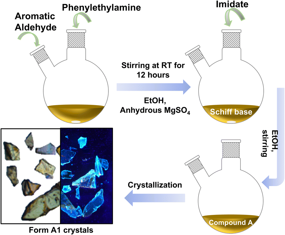 | ||
| Fig. 1 Schematic diagram of the growth of a Form A1 single crystal. | ||
2.2. Material characterization
The absorption spectra and photoluminescence of the Form A1 crystal were measured using a UV-Vis spectrophotometer (model UV 3092, Labindia) and a fluorescence spectrometer (Edinburgh Instruments, Model FS5 spectrofluorometer), respectively. High-resolution transmission electron microscopy (HRTEM) images were obtained with the JEOL JEM F-200 instrument, operating at 200 kV. The CSI Nano-Observer AFM instrument was utilized to measure the topography. Kelvin probe force microscopy (KPFM) was used to measure the work function of the sample, which works by measuring the contact potential difference (CPD) between a conductive AFM tip and the sample surface, analyzing long-range electrostatic forces generated by the probe–sample interactions.30 The Pt/Ir coated calibrated KPFM tip with a work function (Φ) value of 4.85 eV was utilized for the surface potential measurements. Furthermore, the crystal was analysed using density functional theory (DFT) and time-dependent density functional theory (TD-DFT) calculations performed with the Gaussian 09 software package. The B97D3![[thin space (1/6-em)]](https://www.rsc.org/images/entities/char_2009.gif) 31 functional, incorporating Grimme's D332 dispersion correction, was employed at the 6-311G(d,p)33 basis set level to evaluate the HOMO–LUMO gap and to gain insights into the UV-Vis absorption spectra (Fig. 3 and 7).
31 functional, incorporating Grimme's D332 dispersion correction, was employed at the 6-311G(d,p)33 basis set level to evaluate the HOMO–LUMO gap and to gain insights into the UV-Vis absorption spectra (Fig. 3 and 7).
2.3. Experimental setup for photocurrent analysis
The photodetector device was fabricated using a single crystal of A1 GFP, which was carefully positioned on a silicon nitride substrate. The crystal was aligned on the substrate to achieve optimal contact and effective interaction with the incident light. Silver (Ag) paste was carefully applied to form source and drain contacts on the crystal to establish electrical connections. The silver paste was chosen due to its excellent conductivity and ease of application, enabling low-resistance electrical pathways.34 The contacts were manually placed using a precision tip to ensure minimal damage to the crystal surface and uniform distribution of the paste, thereby enhancing charge injection and minimizing contact-related losses. The photocurrent measurements of the crystal were evaluated in a probe station (EPS150TRIAX, Cascade Microtech) (Fig. 2). A Keithley 2634B source meter was employed to measure the electrical response, including I–V curves and time dependent photocurrent. The device was illuminated with two available laser sources at 532 nm (486 mW cm−2) and 632 nm (78 mW cm−2) and a broadband halogen lamp for photocurrent measurements. The effective illumination area of the crystal was approximately 36 μm2, and the light was directed onto the active region to ensure uniform exposure. The power density of all light sources was calibrated and maintained at a constant level throughout the experiments to ensure reproducibility and allow for direct comparison of the device performance under different illumination conditions. The time-dependent photocurrent measurements of the device were recorded at several applied bias voltages, ranging from ±2 V, ±5 V, ±7.5 V, ±10 V, ±15 V, to ±20 V. This was done to evaluate the device's responsivity under various operating conditions. The dynamic response of the photodetector was measured under ON/OFF light cycles at five second intervals to assess its stability, rise time, and decay time at each bias voltage.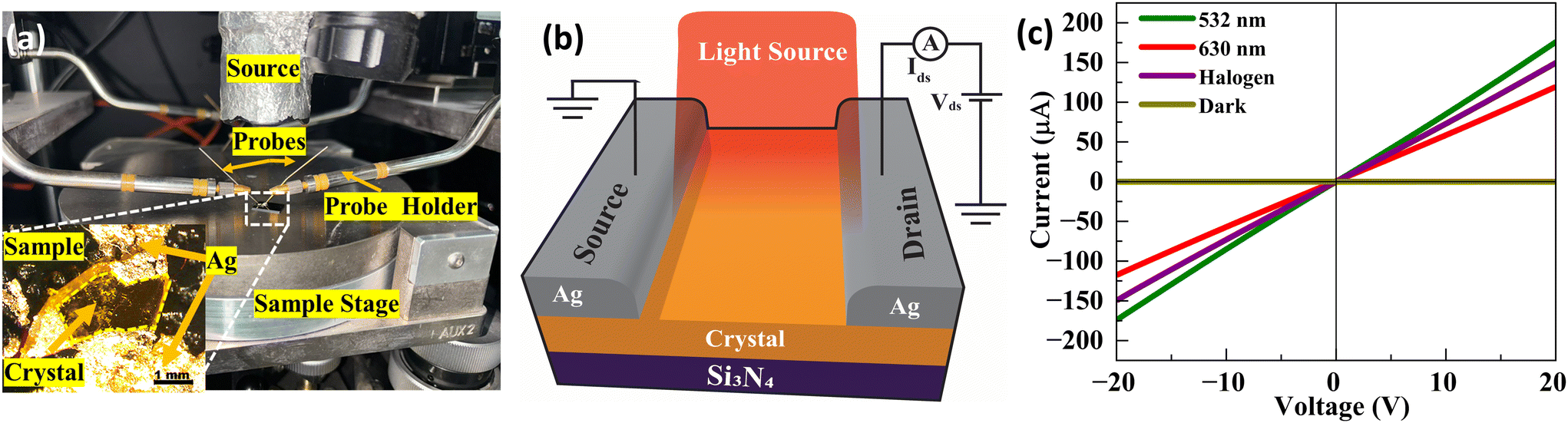 | ||
| Fig. 2 (a) Experimental setup: MPS150 Cascade Microtech EPS150TRIAX probe station. Inset shows the optical image of the crystal. (b) Schematics of the photocurrent measurement. (c) I–V curves of Form A1 crystal under 532 nm, 630 nm, and halogen illumination and in the dark. | ||
3. Results and discussion
3.1. Characterization and measurements
Photoluminescence (PL) and absorption properties were studied through optical characterisation studies. Fig. 3(a) shows the absorption and emission spectra of the crystal at ambient temperature within the wavelength range of 300–700 nm. The analysis revealed an absorption maximum at 400 nm and an emission peak at 449 nm, which corresponds to the crystal's characteristic blue emission. The optical bandgap of the material was calculated using the Tauc relation, yielding a value of 2.84 eV. This value closely matches the theoretical values predicted by DFT calculations. This consistency between experimental and computational results emphasizes the material's optical properties and applicability for visible-range photodetection applications.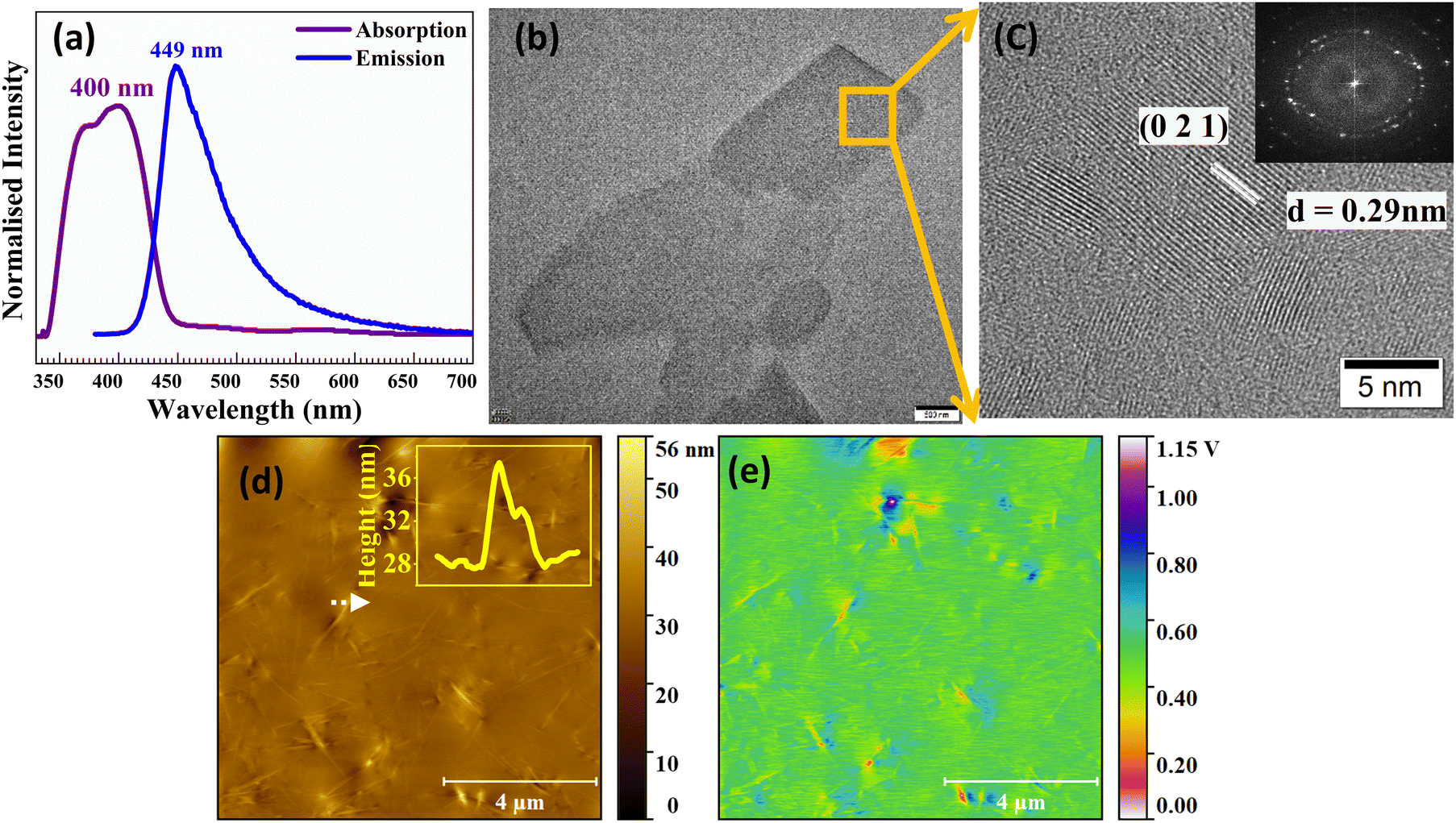 | ||
| Fig. 3 (a) The Form A1 absorption and photoemission spectra, (b and c) HRTEM image of the crystal (inset shows the SAED pattern), (d) AFM micrograph of the crystal with the inset illustrating the height profile indicated by the white dashed line, and (e) surface potential map obtained by KPFM. | ||
HRTEM of Form A1 crystal was performed. Fig. 3(b and c) reveal well-defined lattice fringes, indicating a high degree of crystallinity, essential for charge transport and optoelectronic applications.35 The lattice fringes observed in the HRTEM micrographs correspond to an interplanar spacing of approximately 0.29 nm, which represents the (021) plane. The selected area electron diffraction (SAED) pattern represents the single crystalline nature of the material.
An atomic force microscope (AFM) in tapping mode was employed over a 10 × 10 μm2 area to characterize the surface morphology, as shown in Fig. 3(d). The inset shows the height profile, indicating a relatively smooth and uniform surface profile, which is crucial for reliable photodetector performance.
To further characterize the electrical properties of the crystal, we performed KPFM measurements, an electrical mode of AFM that allows for the determination of work function, surface potential and charge distribution.36Fig. 3(e) portrays the surface mapping of the crystal over a 10 × 10 μm2 area. The CPD between the tip and the sample is expressed as37
 | (1) |
| (Φsample − Φtip) ≈ 0.4 eV, | (2) |
| Φsample ≈ 5.25 eV, | (3) |
3.2. Time-dependent photocurrent analysis
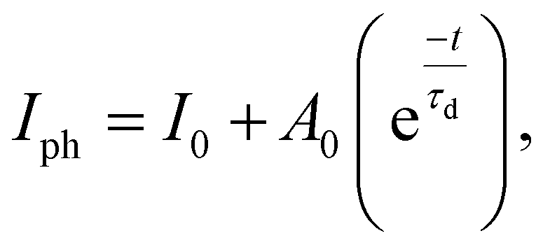
Fig. 4 depicts the time-dependent photocurrent response of the Form A1 GFP single crystal photodetector at six different bias voltages under illumination from three different light sources, with ‘ON’ indicating the light exposure. The photocurrent Iph was estimated using the relationship Iph = Ilight − Idark, where Ilight and Idark are the currents measured when the lights were turned ON and OFF, respectively. The photocurrent exhibited a clear dependence on the applied bias voltage, indicating enhanced separation and drift of photogenerated carriers, with the maximum photocurrent observed at −20 V for all light sources. Specifically, the 532 nm laser at 486 mW cm−2 shows the highest response, with the photocurrent increasing from 0.008 μA at −2 V to 1.73 μA at −20 V. Also, a maximum photocurrent of 0.06 μA for 630 nm at 78 mW cm−2 and 1.0 μA for the halogen lamp is observed. This indicates that the material's optimal sensitivity is in the visible spectrum. The device also demonstrated excellent photocurrent stability across multiple ON/OFF cycles, showing consistent and repeatable behaviour under all light sources, emphasizing the material's robustness and reliability.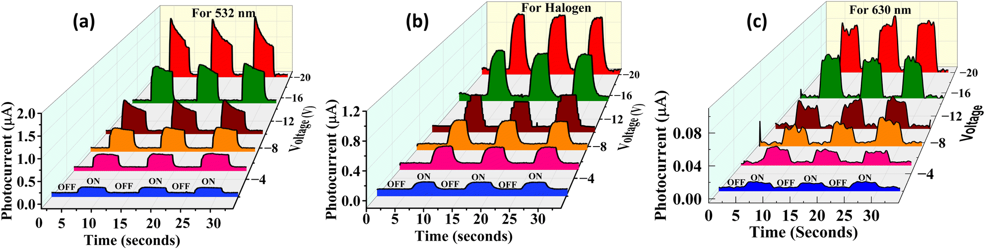 | ||
| Fig. 4 Time dependent photocurrent measurements for various applied bias voltages. Photoresponse to (a) 532 nm, (b) halogen and (c) 630 nm illumination sources. | ||
For comparative analysis of the photoresponse to different light sources, we plotted the time-dependent photocurrent curves for various voltages, as shown in Fig. 5. This highlights the photodetector's wavelength selective sensitivity and performance consistency under varying illumination sources and bias conditions. Furthermore, the device maintained excellent photocurrent stability across all light sources, with negligible fluctuation in current during repeated ON/OFF cycles, indicating reliable performance under various illumination sources.
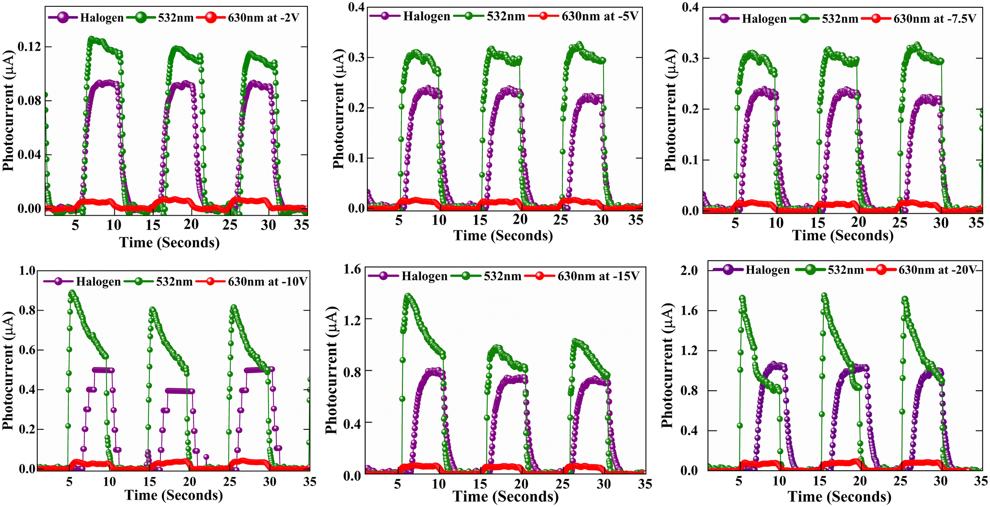 | ||
| Fig. 5 Photocurrent analysis in response to illumination with a halogen lamp, 532 nm laser, and 630 nm laser fixed at −2 V, −5 V, −7.5 V, −10 V, −15 V, and −20 V, respectively. | ||
3.3. Performance parameters of a photodetector
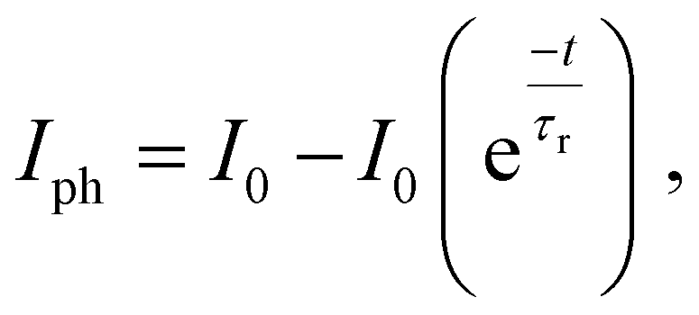
The performance of a photodetector device was evaluated based on different figures of merit. To examine the device's photoresponse, it is essential to evaluate some of the important parameters, which include responsivity, detectivity, rise time, decay time, noise equivalent power and external quantum efficiency.Responsivity, which refers to the ratio of output photocurrent to the power of incident light at a given wavelength, provides a direct measure of the device's efficiency in converting light into optical signals38,39 In this study, the responsivity of the A1 GFP photodetector was found to rise significantly upon applying bias voltage, reaching a maximum of 98.89 mA W−1 at −20 V under 532 nm illumination. This enhanced responsivity at higher bias voltages can be attributed to the increased separation and mobility of photogenerated carriers, leading to stronger photocurrent.40 This shows the superior performance of the device in the visible spectrum. This characteristic is crucial for imaging or optical communication applications, where precise light detection in specific wavelengths is needed.
Detectivity, expressed in cm Hz1/2 W−1 or Jones, measures the photodetector's sensitivity to weak optical signals.41 It considers both the responsivity and noise in the system, which provides a more comprehensive measure of performance. Our photodetector exhibits a maximum detectivity of 7.94 × 10⁸ Jones at 532 nm under −20 V bias, making it highly competitive with conventional organic photodetectors. The high detectivity is associated with low dark current and efficient charge transport within the A1 GFP crystal structure.12 This minimizes thermal noise and improves the signal-to-noise ratio, enabling the device to detect faint light signals precisely.
These responsivity and detectivity parameters can be calculated using eqn (4) and (5).
 | (4) |
 | (5) |
This indicates that the responsivity is a function of both the effective area and the laser power. Fig. 6(a and b) show the responsivity and detectivity response of the device at various applied voltages and in response to both laser wavelengths. Higher bias voltages resulted in increased responsivity for all light sources. Table 1 presents the photocurrent response of Form A1 single crystals to various laser wavelengths and applied voltages. EQE and NEP, two additional performance parameters, were also extracted using the following equations:
 | (6) |
 | (7) |
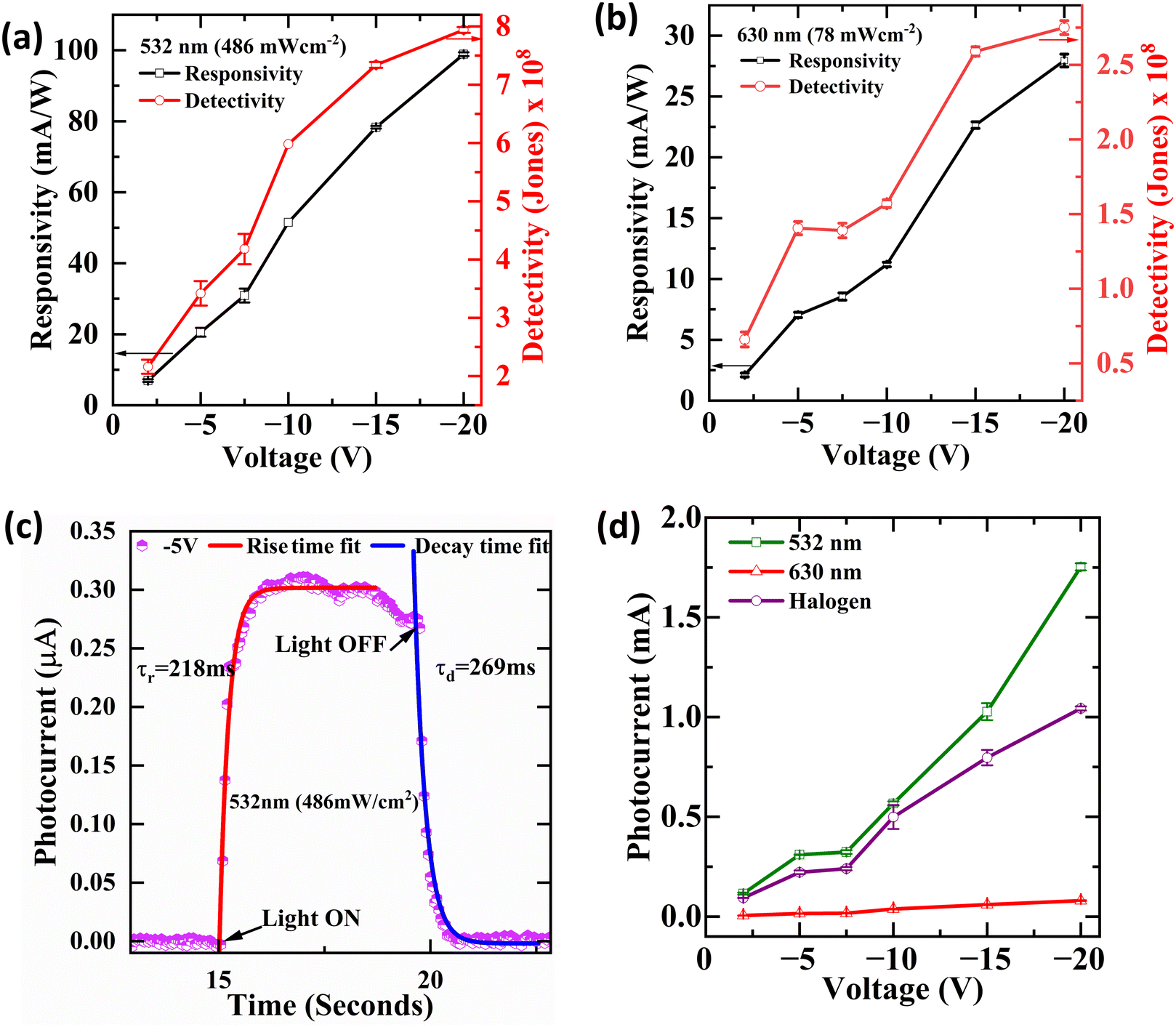 | ||
| Fig. 6 Responsivity and detectivity of the device under (a) 532 nm and (b) 630 nm illumination. (c) Decay and rise times of photocurrent. (d) Photocurrent vs. voltage response under 532 nm, 630 nm and halogen illumination. | ||
| Laser wavelength (nm) | Bias voltage (V) | Responsivity (mA W−1) | Detectivity (Jones) | Rise time (ms) | Decay time (ms) | EQE (%) | NEP (W Hz−1/2) |
|---|---|---|---|---|---|---|---|
| 532 | −2 | 6.94 | 2.09 × 10⁸ | 279 | 217 | 1.62 | 2.30 × 10⁻¹¹ |
| −5 | 20.56 | 3.09 × 10⁸ | 218 | 186 | 4.80 | 2.52 × 10⁻¹¹ | |
| −7.5 | 30.91 | 4.09 × 10⁸ | 232 | 238 | 7.21 | 2.53 × 10⁻¹¹ | |
| −10 | 51.49 | 4.33 × 10⁸ | 194 | 208 | 12.01 | 2.28 × 10⁻¹¹ | |
| −15 | 78.32 | 6.83 × 10⁸ | 159 | 191 | 18.27 | 2.29 × 10⁻¹¹ | |
| −20 | 98.89 | 7.38 × 10⁸ | 180 | 152 | 23.07 | 2.38 × 10⁻¹¹ | |
| 630 | −2 | 2.10 | 6.66 × 10⁷ | 593 | 536 | 0.49 | 4.14 × 10⁻¹¹ |
| −5 | 7.04 | 1.41 × 10⁸ | 553 | 431 | 1.64 | 3.58 × 10⁻¹¹ | |
| −7.5 | 8.55 | 1.39 × 10⁸ | 434 | 511 | 2.00 | 3.99 × 10⁻¹¹ | |
| −10 | 11.18 | 1.57 × 10⁸ | 547 | 484 | 2.61 | 4.04 × 10⁻¹¹ | |
| −15 | 22.64 | 2.59 × 10⁸ | 480 | 533 | 5.28 | 3.49 × 10⁻¹¹ | |
| −20 | 27.95 | 2.75 × 10⁸ | 547 | 585 | 6.52 | 3.65 × 10⁻¹¹ |
The EQE, which measures the number of charge carriers generated per incident photon, demonstrates the superior performance of this GFP-based photodetector (Table 2).42 At 532 nm, the EQE reaches 23.07% under −20 V bias, significantly improving the photodetection capabilities by effectively converting incoming photons into electrical signals. Despite a reduced bias of −2 V, the EQE remained stable at 1.62%, demonstrating the material's capacity to sustain good performance under diverse operating conditions. The enhanced EQE is crucial for applications that require efficient light-to-electrical energy conversion, including imaging systems and optical sensors. The NEP refers to the minimal optical power needed for the detector to generate a signal that is comparable to the noise level, thereby defining the weakest light signal detectable by the device.43
| Parameters | Values | |
|---|---|---|
| Experimental | Light sources | 532 nm (486 mW cm−2) |
| 630 nm (78 mW cm−2) | ||
| Halogen lamp | ||
| Active device area | 36 μm2 | |
| Temperature | Room temperature | |
| Substrate | Silicon nitride | |
| Material | λ ex | 400 nm |
| λ em | 449 nm | |
| Bandgap energy | ∼2.84 eV |
A lower NEP value reflects a more sensitive photodetector. This study reveals that the A1 GFP photodetector exhibits an NEP value of 2.38 × 10⁻¹¹ W Hz−1/2 at 532 nm with a −20 V bias, signifying remarkable sensitivity within the visible spectrum. The NEP is notably low even at lowered bias voltages (e.g., 2.3 × 10⁻¹¹ W Hz−1/2 at −2 V), confirming the detector's capability to function efficiently at lower power levels. The photocurrent demonstrates a sharp response to the incident light upon illumination (Table 1). Fig. 6(c) depicts the measured and fitted data for the rise times and decay times. The time constants for rise time and decay time are calculated using eqn (8) and (9).
 | (8) |
 | (9) |
As shown in Fig. 6(d), the photocurrent vs. voltage plot highlights the stability and reproducibility of the A1 GFP photodetector's performance. This indicates minimal fluctuations in photocurrent, demonstrating a consistent response across multiple measurements. The photocurrent rises proportionally with voltage, reaching its maximum at −20 V, reflecting optimal carrier separation and mobility. The device also shows reliable performance at lower voltages, making it suitable for low-power applications.
A comparative analysis of the performance metrics (responsivity and detectivity) of the A1 GFP analogue and other reported materials is presented in Table 3. This comparison highlights the significant advancements achieved in this work. Notably, the A1 GFP single crystal exhibits a comparative responsivity to conventional organic and inorganic photodetectors reported in recent literature. The table further shows that the rise and decay times of the A1 GFP device are competitive, with values of 180 ms and 152 ms, respectively, demonstrating fast photoresponse dynamics compared to other materials. This comprehensive comparison positions the A1 GFP analogue as a superior candidate for next-generation visible-range photodetectors, providing a balance between high sensitivity, fast response, and robust material stability.
| Material | λ (nm) | Bias (V) | R (mA W−1) | D (Jones) | Ref. |
|---|---|---|---|---|---|
| MoS2/g-C3N4 | 532 | −9 | 700 | 8 × 10¹⁰ | 44 |
| ZnInS4 single crystals | 460 | 10 | 170 | 1.7 × 10¹² | 45 |
| Benzothiophene | 405 | — | 420 | — | 46 |
| PBTB | 1122 | 8 | 0.96 | — | 47 |
| Alq3 | 254 | 5 | 14.5 | 2.0 × 10¹² | 48 |
| TESAN-BT | 550 | 70 | 50 | 2 × 10⁹ | 49 |
| Graphene/pentacene/PTCDI-C8 | 480 | — | 7 | 2 × 10⁹ | 50 |
| C60 single crystal arrays | 400 | 10 | 8.0 | 7.08 × 10⁸ | 51 |
| Form A1 crystal | 532 | −20 | 98.89 | 7.94 × 10⁸ | This work |
| 630 | −20 | 27.95 | 2.75 × 10⁸ |
3.4. Computational studies
Density functional theory (DFT) calculations were carried out on the Form A1 crystal using the B97D3/6-311G(d,p) level of theory. The HOMO to LUMO gap explains the charge transport mechanism within the Form A1 crystal, where electron density is transferred from the conjugated imidazole moiety and the trimethoxybenzene moiety in the outer regions to the inner parts of the same moieties, as illustrated in Fig. 7. Time-dependent density functional theory (TD-DFT) calculations at the B97D3 level were performed to compare the experimentally obtained bandgap of the Form A1 crystal. It was observed that the transition corresponding to λmax (fosc = 0.5616, calcdλabs = 419.64 nm, and expλabs = 400 nm) originates from a π → π* transition between the HOMO and the LUMO+3 orbitals. During this transition, the HOMO is predominantly delocalized across the π molecular orbitals of the conjugated imidazole and trimethoxybenzene rings, and the LUMO gets delocalized across the π* molecular orbitals of the same rings and the π* orbitals of the C![[double bond, length as m-dash]](https://www.rsc.org/images/entities/char_e001.gif) C bonds. Additionally, the small HOMO–LUMO gap facilitates efficient photoexcitation, allowing the crystal to readily absorb photons and promote electrons from the HOMO to the LUMO. This characteristic improves the ability of the material to generate charge carriers upon light absorption, making it suitable for use in photodetectors. The reduced energy barrier for electron excitation improves its sensitivity to light, enabling faster response times and efficient photocurrent generation, which are essential properties for photodetection applications.
C bonds. Additionally, the small HOMO–LUMO gap facilitates efficient photoexcitation, allowing the crystal to readily absorb photons and promote electrons from the HOMO to the LUMO. This characteristic improves the ability of the material to generate charge carriers upon light absorption, making it suitable for use in photodetectors. The reduced energy barrier for electron excitation improves its sensitivity to light, enabling faster response times and efficient photocurrent generation, which are essential properties for photodetection applications.
 | ||
| Fig. 7 The molecular orbitals along with their energy levels calculated using the B97D3/6-311G(d,p) level of theory. | ||
3.5. Discussion and future prospects
The Form A1 crystal shows better efficiency for the generation of free charge carriers upon light absorption and charge transport under the influence of external potential. The delocalized nature of the π-conjugated system in the molecule facilitates efficient charge transport, allowing separated charges to migrate towards the electrodes, which is crucial for photodetector performance. Although our device shows excellent photodetection performance in the visible spectrum, future studies should explore the photodetector's sensitivity across a broadband spectrum from UV and near-infrared (NIR) regions. The performance of the device has been studied under constant laser power settings; however, it can be explored for varying laser intensities, which could provide deeper insights into its photodetection performance. It should be noted that the experiments in this work were performed under controlled environmental conditions, i.e., at ∼25 °C and humidity: 50–60%. Therefore, further studies under varied environmental conditions will be required to assess the device's performance, stability, and robustness for its practical deployment, particularly in wearable or outdoor devices. Furthermore, other analogues of this family can be synthesised and studied for high-performance broadband photodetectors with good stability and mechanical flexibility.In medical diagnostics, it can be used in non-invasive monitoring devices like smartwatches or skin sensors to track vital signs using light-based methods. Its biocompatibility and high sensitivity make it ideal for implantable biosensors and optical communication systems, ensuring real-time data transmission and environmental sensing. Furthermore, the GFP-based photodetector holds significant promise for practical applications in flexible electronics, such as foldable displays and wearable devices, where its flexibility and lightweight nature allow seamless integration.
4. Conclusions
In this study, we successfully demonstrate the potential of a green fluorescent protein (GFP) chromophore analogue as an organic single-crystal photodetector, particularly for visible-range applications. The synthesized A1 GFP crystals exhibit significant values of device parameters, including responsivity and detectivity. A peak photocurrent of 1.73 μA was achieved under a bias voltage of −20 V. The photodetector's rapid response times, characterized by short rise and decay times, further highlight its suitability for fast photodetection applications. These features make the A1 GFP analogue highly adaptable for next-generation technologies.Author contributions
V. V.: conceptualization, writing – original draft and formal analysis; N. D.: methodology; S. V.: resources and validation; A. K.: editing and validation; R. P.: resources; S. H.: methodology, resources, and review & editing; R. G.: resources; K. V.: resources; R. K.: supervision, project administration, methodology, conceptualization and review & editing.Data availability
The data supporting the findings of this work are available within the article.Conflicts of interest
There are no conflicts to declare.Acknowledgements
The authors acknowledge the Director of CSIR-NCL, Pune, India, for the opportunity and infrastructure to conduct this research, and the Director of CSIR-NPL, Delhi, India, for providing the experimental facility and guidance. V. V. acknowledges DST and INSPIRE (DST/INSPIRE/03/2023/000261) for the research fellowship. The financial support from the Science and Engineering Research Board (SERB), New Delhi (Grant No. CRG/2022/004504), is acknowledged by R.G.G. and R.V.K. K. V. acknowledges DST-SERB (CRG/2021/003255) for financial support. For computational facilities, R. P. and K. V. acknowledge the Multi-Scale Simulation and Modeling (MSM) project. The “PARAM Brahma Facility” under the National Supercomputing Mission, Government of India (IISER, Pune), is acknowledged.References
- Y.-L. Wu, K. Fukuda, T. Yokota and T. Someya, Adv. Mater., 2019, 31, 1903687 CrossRef CAS PubMed.
- C. M. Lochner, Y. Khan, A. Pierre and A. C. Arias, Nat. Commun., 2014, 5, 5745 CrossRef CAS PubMed.
- Y. Wang, J. Benduhn, L. Baisinger, C. Lungenschmied, K. Leo and D. Spoltore, ACS Appl. Mater. Interfaces, 2021, 13, 23239–23246 CrossRef CAS PubMed.
- M. Babics, H. Bristow, W. Zhang, A. Wadsworth, M. Neophytou, N. Gasparini and I. McCulloch, J. Mater. Chem. C, 2021, 9, 2375–2380 RSC.
- B. Biswas and B. Saha, Phys. Rev. Mater., 2019, 3, 020301 CrossRef CAS.
- M. Shahbaz, M. A. Butt and R. Piramidowicz, Micromachines, 2023, 14, 1637 CrossRef PubMed.
- J. E. Carey and E. Mazur, Conference on Lasers and Electro-Optics/International Quantum Electronics Conference and Photonic Applications Systems Technologies, San Francisco, California, 2004 Search PubMed.
- W. Si, W. Zhou, X. Liu, K. Wang, Y. Liao, F. Yan and X. Ji, Micromachines, 2024, 15, 427 CrossRef PubMed.
- Q. Li, Y. Guo and Y. Liu, Chem. Mater., 2019, 31, 6359–6379 CrossRef CAS.
- C. Fuentes-Hernandez, W.-F. Chou, T. M. Khan, L. Diniz, J. Lukens, F. A. Larrain, V. A. Rodriguez-Toro and B. Kippelen, Science, 2020, 370, 698–701 CrossRef CAS PubMed.
- Y. Xu and Q. Lin, Appl. Phys. Rev., 2020, 7, 011315 CAS.
- D. Yang and D. Ma, Adv. Opt. Mater., 2019, 7, 1800522 CrossRef.
- W. Wu, K. Chen, T. Wang, N. Wang, X. Huang, L. Zhou, Z. Wang and H. Hao, J. Mater. Chem. C, 2023, 11, 2026–2052 RSC.
- S. Qin, X. Qin, Q. Du, Y. Gan, Y. Zhang, A. Wang, X. Yan, R. Dong, Y. Liu, S. Li, C. Liu, W. Wang and F. Wang, J. Mater. Chem. C, 2022, 10, 11710–11718 RSC.
- M. Wang, Y. Xiao, Y. Li, L. Han, Z. Sun, L. He, R. Liu and K. Hu, Materials, 2022, 15, 4820 CrossRef CAS PubMed.
- Q. Du, Z. Wang Du, M. Li Du, Y. Gan, S. Li, Y. Liu, W. Wang, F. Wang and S. Qin, J. Mater. Chem. C, 2023, 11, 5182–5189 RSC.
- H. Lee, E. Kim, Y. Lee, H. Kim, J. Lee, M. Kim, H.-J. Yoo and S. Yoo, Sci. Adv., 2018, 4, eaas9530 CrossRef CAS PubMed.
- N. Li, N. Eedugurala, D.-S. Leem, J. D. Azoulay and T. N. Ng, Adv. Funct. Mater., 2021, 31, 2100565 CrossRef CAS.
- H.-R. Lim, H. S. Kim, R. Qazi, Y.-T. Kwon, J.-W. Jeong and W.-H. Yeo, Adv. Mater., 2020, 32, 1901924 CrossRef CAS PubMed.
- D. Tordera, B. Peeters, H. B. Akkerman, A. J. J. M. van Breemen, J. Maas, S. Shanmugam, A. J. Kronemeijer and G. H. Gelinck, Adv. Mater. Technol., 2019, 4, 1900651 CrossRef CAS.
- G. Simone, M. J. Dyson, S. C. J. Meskers, R. A. J. Janssen and G. H. Gelinck, Adv. Funct. Mater., 2020, 30, 1904205 CrossRef CAS.
- Z. He, J. Han, X. Du, L. Cao, J. Wang, C. Zheng, H. Lin and S. Tao, Adv. Funct. Mater., 2021, 31, 2103988 CrossRef CAS.
- H. T. Chandran, H. Tang, T. Liu, S. Mahadevan, K. Liu, Z. Lu, J. Huang, Z. Ren, F. Liao, Y. Chai, P. W. Fong, S.-W. Tsang, S. Lu and G. Li, Mater. Horiz., 2023, 10, 918–927 RSC.
- Z. Qi, J. Cao, H. Li, L. Ding and J. Wang, Adv. Funct. Mater., 2015, 25, 3138–3146 CrossRef CAS.
- B. Nath, P. C. Ramamurthy, D. R. Mahapatra and G. Hegde, IEEE International Conference on Flexible and Printable Sensors and Systems (FLEPS), Vienna, Austria, 2022, pp. 1–4 Search PubMed.
- N. B. Dabke, Y. Raut, B. P. Mali, R. Pandya, K. Vanka, K. Manoj and R. G. Gonnade, J. Mater. Chem. C, 2024, 12, 8368–8379 RSC.
- G. G. Lambert, G. Gotthard, D. T. Schultz, I. Navizet and T. Lambert, et al. , PLoS Biol., 2020, 18, 1–22 CrossRef PubMed.
- F. Tian, G. Xu, S. Zhou, S. Chen and D. He, Analyst, 2023, 148, 2882–2891 RSC.
- A. Baldridge, J. Kowalik and L. M. Tolbert, Synthesis, 2010, 2424–2436 CAS.
- S. Grimme, S. Ehrlich and L. Goerigk, J. Comput. Chem., 2011, 32, 1456–1465 CrossRef CAS PubMed.
- S. Grimme, J. Antony, S. Ehrlich and H. Krieg, J. Chem. Phys., 2010, 132, 154104 CrossRef PubMed.
- A. D. McLean and G. S. Chandler, J. Chem. Phys., 1980, 72, 5639–5648 CrossRef CAS.
- Y. Hwang, Y. H. Hwang, K. W. Choi, S. Lee, S. Kim, S. J. Park and B.-K. Ju, Sci. Rep., 2021, 11, 10499 CrossRef CAS PubMed.
- T. Xiao, J. Wang, S. Yang, Y. Zhu, D. Li, Z. Wang, S. Feng, L. Bu, X. Zhan and G. Lu, J. Mater. Chem. A, 2020, 8, 401–411 RSC.
- M. Nonnenmacher, M. P. O'Boyle and H. K. Wickramasinghe, Appl. Phys. Lett., 1991, 58, 2921–2923 CrossRef.
- S. Sorifi, S. Kaushik and R. Singh, Nanoscale Adv., 2022, 4, 479–490 RSC.
- R. Shikler, T. Meoded, N. Fried, B. Mishori and Y. Rosenwaks, J. Appl. Phys., 1999, 86, 107–113 CrossRef CAS.
- W. Feng, J.-B. Wu, X. Li, W. Zheng, X. Zhou, K. Xiao, W. Cao, B. Yang, J.-C. Idrobo, L. Basile, W. Tian, P. Tan and P. Hu, J. Mater. Chem. C, 2015, 3, 7022–7028 RSC.
- L. Lv, J. Yu, X. Sui, J. Wu, X. Dong, G. Lu, X. Liu, A. Peng and H. Huang, J. Mater. Chem. C, 2019, 7, 5739–5747 RSC.
- K. Roy, M. Padmanabhan, S. Goswami, T. P. Sai, G. Ramalingam, S. Raghavan and A. Ghosh, Nat. Nanotechnol., 2013, 8, 826–830 CrossRef CAS PubMed.
- S. Verma, R. Yadav, A. Pandey, M. Kaur and S. Husale, Sci. Rep., 2023, 13, 197 CrossRef CAS PubMed.
- X. Liu, D. Wang, P. Shao, H. Sun, S. Fang, Y. Kang, K. Liang, H. Jia, Y. Luo, J. Xue, J. Wang, T. Zhi, D. Chen, B. Liu, S. Long and R. Zhang, Adv. Funct. Mater., 2022, 32, 2201604 CrossRef CAS.
- I. K. Kim, J. H. Jo, J. Lee and Y. J. Choi, Org. Electron., 2018, 57, 89–92 CrossRef CAS.
- D. B. Velusamy, M. A. Haque, M. R. Parida, F. Zhang, T. Wu, O. F. Mohammed and H. N. Alshareef, Adv. Funct. Mater., 2017, 27, 1605554 CrossRef.
- L. Valdman, V. Mazánek, P. Marvan, M. Serra, R. Arenal and Z. Sofer, Adv. Opt. Mater., 2021, 9, 2100845 CrossRef CAS.
- Y. Zhou, L. Wang, J. Wang, J. Pei and Y. Cao, Adv. Mater., 2008, 20, 3745–3749 CrossRef CAS.
- L. Lv, W. Dang, X. Wu, H. Chen, T. Wang, L. Qin, Z. Wei, K. Zhang, G. Shen and H. Huang, Macromolecules, 2020, 53, 10636–10643 CrossRef CAS.
- Y. Zhang, J. Jie, Y. Sun, S. G. Jeon, X. Zhang, G. Dai, C. J. Lee and X. Zhang, Small, 2017, 13, 1604261 CrossRef PubMed.
- D. S. Chung, Y.-H. Kim and J.-S. Lee, Nanotechnology, 2014, 25, 035202 CrossRef CAS PubMed.
- J. S. Kim, Y. J. Choi, H. J. Woo, J. Yang, Y. J. Song, M. S. Kang and J. H. Cho, Adv. Funct. Mater., 2017, 27, 1704475 CrossRef.
- S. Zheng, X. Xiong, Z. Zheng, T. Xu, L. Zhang, T. Zhai and X. Lu, Carbon, 2018, 126, 299–304 CrossRef CAS.
| This journal is © The Royal Society of Chemistry 2025 |