
 Open Access Article
 This Open Access Article is licensed under a Creative Commons Attribution-Non Commercial 3.0 Unported Licence
Layer-controlled continuous MoS2 growth using a spin-coatable metal precursor buffer†
Dong Hwan Kim‡
 a,
Jinyoung Seo‡b,
Yoonbeen Kangb,
Bumjun Leeb and
Sang-Yong Ju*ab
a,
Jinyoung Seo‡b,
Yoonbeen Kangb,
Bumjun Leeb and
Sang-Yong Ju*ab
aGraduate Program of Semiconductor Science and Engineering, Yonsei University, Seoul 03722, Republic of Korea. E-mail: syju@yonsei.ac.kr
bDepartment of Chemistry, Yonsei University, Seoul 03722, Republic of Korea
First published on 21st May 2025
Abstract
Continuous large-area MoS2 growth holds significant potential for next-generation optoelectronic applications, yet achieving it efficiently and reproducibly with the conventional chemical vapor deposition (CVD) process remains a challenge due to inconsistent precursor adsorption and non-uniform nucleation. In this study, we developed a pH-optimized metal precursor buffer that enables uniform spin-coating and facilitates continuous MoS2 growth. Sodium cholate (SC) acts as both a dispersant and a buffer, transforming molybdenum oxide into a dispersion-stable sodium molybdate (Na2MoO4)/SC complex. This complex forms a stable, uniformly spin-coatable dispersion at pH = 5.3, allowing it to form hydrogen bonds with the SiO2/Si substrate. Additionally, increasing the complex concentration enhances precursor adsorption, enabling controlled MoS2 layer formation via CVD. Using this approach, we successfully fabricated continuous, centimeter-scale MoS2 films in varying layer numbers. Real-time observation reveals the growth kinetics of the continuous MoS2 film in terms of contrast value, according to the reaction time and temperature, indicating that the growth can occur at temperatures as low as 500 °C. This stable, scalable, and reproducible spin-coating technique, utilizing a metal precursor buffer, offers a robust pathway for producing large-area transition metal chalcogenide structures, advancing the development of 2D material-based applications.
Introduction
Transition metal dichalcogenides (TMCs) possess unique optoelectronic properties1–4 and tunabilities5–8 essential for various advanced applications, including field-effect transistors,2,9–12 spintronics,13–17 and photocatalysis.18,19 Achieving large-area, high-quality TMC structures necessitates precise and reproducible control over the growth process. Among the widely used techniques, chemical vapor deposition (CVD), which employs metal and chalcogen precursors,20–26 plays a crucial role in facilitating controlled and scalable TMC growth.Alkali halide molten salts22,24–29 have been identified as rapid and reproducible catalysts for converting metal precursors into various TMCs via CVD growth. For example, Li et al.24 demonstrated that sodium chloride promotes the growth of MoS2 nanoribbons through the vapor–liquid–solid (VLS) mechanism. They also emphasized that alkali metals, rather than halides, play a more crucial role in MoS2 formation. A recent study using an integrated chemical vapor deposition microscope (ICVDM) revealed that sodium particles acted as catalysts, enhancing growth by scooting along MoS2 grain edges and facilitating MoS2 laminate precipitation.26 Consequently, sodium22,25–27,29 plays a pivotal role in the growth process, and controlling its activity presents a potential strategy for achieving large-area, high-quality TMC growth.
Among various molybdenum precursors, molybdenum oxide (MoO3) and sodium molybdate (Na2MoO4) are widely used for MoS2 growth. In the CVD process, MoO3 is typically sublimed from a crucible onto a target substrate to form MoS2,20,21,30,31 while Na2MoO4 is directly coated onto the substrate as a metal precursor.25,29 Notably, Na2MoO4 contains sodium catalyzing the MoS2 growth.25 Recently, Li et al.25 reported that whereas a continuous MoS2 film has been successfully grown on a sapphire substrate using Na2MoO4, achieving the same on SiO2/Si substrates remains challenging. This infers that surface charges on both the metal precursor and the substrate play a crucial role in precursor adsorption and the formation of a continuous MoS2 film.
In this study, we successfully achieved continuous centimeter-scale polycrystalline MoS2 growth using a spin-coatable metal precursor buffer via the CVD method. Sodium cholate (SC), serving as both a dispersant and a buffer, converts layered MoO3 into a monomeric Na2MoO4/SC complex upon sonication, enabling uniform spin-coating on O2-plasma-treated SiO2 substrates. Additionally, the uniform spin-coating of metal precursors allows precise control over the number of MoS2 layers across large areas, depending on the metal precursor concentration. The polycrystalline nature of the MoS2 film was confirmed through transmission electron microscopy (TEM). Real-time observation of continuous MoS2 formation provided insights into the growth pathway, as well as the relationship between temperature and time. Furthermore, the spin-coatable precursor demonstrated facile patterning capability, highlighting its potential for integration with other devices.
Experimental
Materials and instrumentation
Molybdenum(VI) oxide (purity ≥99.5%), sodium molybdate dihydrate (purity ≥99%), and sulfur (purity ≥99.5%) were procured from Merck. SC (purity ≥98%, TCI) was used as is. Deionized (DI) water with resistivity exceeding 18 MΩ cm was used to prepare the Na2MoO4/SC dispersion. Argon gas, with a purity greater than 99.99%, was supplied by Donga Gas and used as the CVD carrier gas. The Si wafer (285 nm thick SiO2/Si substrate, ShinEtsu) was cut into 1 × 1 cm2 pieces, cleaned with methanol, acetone, and isopropanol, and dried using a nitrogen stream. The pH of the dispersions was measured with a SevenMulti pH meter (Mettler Toledo), calibrated with three known pH buffer references (i.e., 4.01, 7.00, and 10.01). The zeta (ζ)-potential was determined in a quartz cuvette using an ELS-1000ZS (Otsuka Electronics) following standard procedures.32 UV-vis absorption spectra were measured using a V-770 spectrophotometer (JASCO) with 1 mm path length cuvettes (21/Q/1, Starna Scientific), and extinction was recorded in a double-beam configuration. Atomic force microscopy (AFM) height images were obtained in tapping mode using an NX10 AFM (Park Systems), with Al-coated silicon cantilevers (force constant: 37 N m−1, resonance frequency: 300 kHz, ACTA-20, App Nano).33 Images were captured at 512 × 512 pixels at a scan speed of 0.2 Hz. Topography flattening was performed using the XEI program (Park Systems) with a polynomial fit along the fast scan axis. Raman measurements in a back-scattering configuration were conducted using either a custom-built Raman system34,35 or the XperRam C (Nanobase) with 532 nm excitation unless noted otherwise. To prevent sample damage, the laser power was kept below 0.1 mW. Optical images were captured with an upright fluorescence microscope (BX-51, Olympus) equipped with a CMOS camera (3.4 μm per pixel, 2560 × 1920 pixels). Water contact angles were measured with a contact angle goniometer (Phoenix 10, Surface Electro Optics) based on previous work.36 X-ray photoelectron spectroscopy (XPS) data were acquired with K-alpha (Thermo Scientific), according to the literature.37 A monochromatic X-ray source (Al Kα: 1486.6 eV) with a beam size of 400 μm was used with a power of 12 kV and 3 mA under vacuum (sample pressure: 4.8 × 10⁻⁹ mbar, base pressure: 2.9 × 10⁻⁹ mbar). Ag 3d5/2 was used as a charging reference for all samples. Survey scans were acquired with 200 eV pass energy at a step size of 1 eV. Detailed scans were obtained at 40 eV pass energy with a step size of 0.1 eV. The acquired spectra were baseline-subtracted using the Shirley profile. The C 1s peak (284.8 eV) from adventitious carbon was used as an internal reference. SC, MoO3, and Na2MoO4 were used in their as-received powder forms. A Na2MoO4/SC dispersion was drop-cast onto a 285 nm thick SiO2/Si substrate, while MoS2, grown on a 285 nm thick SiO2/Si substrate, was cleaned with isopropanol prior to use. Peak fitting employs a Shirley-type background. The S 2p (Mo 3d) spin–orbit doublet separation was held constant at 1.2 (3.1) eV and with a 2![[thin space (1/6-em)]](https://www.rsc.org/images/entities/char_2009.gif) :1 (3:2) area ratio.
:1 (3:2) area ratio.
Surface hydrophilization (step i)
O2-plasma reactive ion etching (RIE, PS-100, Plasol) or inductively coupled plasma (ICP-RIE, IPS-5000, Sntec) was employed to hydrophilize a 285 nm thick SiO2/Si substrate and remove surface contaminants. The hydrophilization process typically involves applying the plasma at 100 W for 7 min. ICP-RIE treatment was conducted at 50 W for 40 s in the presence of O2/CF4 flow with 25 sccm/25 sccm. Spin-coating of the metal precursor dispersion and subsequent steps were performed immediately after the O2-plasma or RIE treatment by minimizing exposure to ambient water.38Metal precursor preparation (step ii)
MoS2 growth (step iii)
All CVD growths were carried out using an ICVDM.26 MoS2 growth: prior to CVD growth, the 285 nm thick SiO2/Si substrate was treated with O2 plasma. Immediately afterward, 100 μL of the Na2MoO4/SC dispersion was spin-coated at 5000 rpm for 1 min on an O2 plasma-treated substrate, which was then placed in a mini-CVD crucible. In a separate alumina crucible, 1000 mg of sulfur was loaded into the sulfur tube furnace. Parameters for the mini-CVD, charge-coupled device (CCD), chalcogen tube furnace, and flow controller were set accordingly. TCVD and TS were ramped to 750 °C and 250 °C, respectively, with an FAr = 180 sccm argon flow. The growth temperature was maintained for 20 min, reached by ramping the temperatures at rates of 42 °C min−1 for sulfur and 100 °C min−1 for the spin-coated sample. After the growth, the system was allowed to naturally cool to room temperature. Real-time images were captured using a long working-distance 50× objective lens (LMPlanFL, working distance: 10.6 mm, N.A.: 0.50, Olympus). A Retiga R6 CCD (Teledyne) was used to collect image stacks, which were then analyzed using the Fiji program. These images were compared with a video containing real-time parameters such as trxn, TCVD, TS, and FAr. Patterned TMC growth: a metal mask was used to create a cross-shaped hydrophilic pattern on the substrate via RIE exposure. Immediately after, the sample was spin-coated with a 6 mM Na2MoO4/SC dispersion and subjected to CVD growth. Sodium particle removal: MoS2 samples were immersed in toluene for 20 min to remove non-covalent sulfur and then dried using nitrogen gas. The samples were subsequently treated with isopropanol to remove sodium until no gas was generated from the surface. CR was obtained using the following equation: CR = (RS − R0)/R0, where RS and R0 denote the reflection intensities of the MoS2 sample on a substrate and bare substrate, respectively.TEM measurements
:1 volume ratio of 36% NH4F and 4.7% HF, 1 nm s−1 etching rate at 25 °C, Merck). The sample was then picked up with a TEM grid, and PMMA was dissolved in acetone. The transferred sample was annealed at 300 °C under 17 mTorr for 1 h using a tube furnace. TEM images were obtained using an aberration-corrected TEM (JEM-ARM 200F Neoarm, Jeol) at 200 kV. HAADF-STEM images were collected at 80 kV after stabilization with TEM accessories, using an aberration-corrected NEOASCOR high-order aberration corrector. Polycrystallinity analysis: Gatan software was utilized to analyze polycrystallinity. The FFT of each TEM image was obtained, and TEM images from specific hexagonal diffraction patterns were generated to indicate each domain. These images were then overlapped to create composite domain-specific TEM images.Results and discussion
Effects of pKa on uniform spin-coating of the precursor dispersion
We hypothesize that the surface charge of the metal precursor plays a crucial role in interacting with the surface charge of the SiO2/Si substrate, thereby influencing uniform coating on the substrate. A transparent Na2MoO4 solution, in which Na2MoO4 is highly soluble in water, exhibits basic pH.40 Considering the reported pKa values of silanol on SiO2 (i.e., 9.8)41 and alumina on sapphire (i.e., 12.2),25 a basic Na2MoO4 solution would create anionic repulsion with silanol moieties on the SiO2/Si substrate, leading to poor adsorption. Therefore, achieving reproducible and continuous MoS2 growth requires a buffered Na2MoO4 solution with mildly acidic pH. To address this, SC functions as both a dispersant and a buffer, converting MoO3 into an Na2MoO4/SC complex. MoO3 was chosen over Na2MoO4 to prevent the formation of sodium chloride during pH adjustment, as sodium chloride has been reported to promote MoS2 nanoribbon growth.24Fig. 1 presents a schematic representation of the process for creating a continuous MoS2 film from the spin-coatable metal precursor buffer via CVD growth (see the Experimental section). The process begins with hydrophilizing a 285 nm thick SiO2/Si substrate through O2-plasma treatment (step i), a crucial step for ensuring uniform spin-coating of the metal precursor dispersion and facilitating subsequent MoS2 growth. Immediately afterward, while minimizing exposure to moisture, the pH-controlled metal precursor dispersion is spin-coated onto the hydrophilized substrate (step ii). This precursor-coated sample is then subjected to CVD growth at 750 °C for 20 min using sulfur and argon gases, converting the precursor into a MoS2 film (step iii). During step ii, moisture can disrupt hydrogen bonding between the spin-coated metal precursor and the hydrophilic substrate, thereby leading to non-uniform adsorption of the metal precursor.
 | ||
| Fig. 1 Schematic of continuous large-area MoS2 growth using spin-coatable pH-controlled SC-buffered metal precursor dispersion. Surface hydrophilization (i): enhancing the SiO2/Si substrate's hydrophilicity via O2 plasma treatment. Precursor spin-coating (ii): depositing a uniform layer of a buffered Na2MoO4/SC dispersion through spin-coating. Inset: illustration of repulsive Na2MoO4/SC particles forming hydrogen bonds with silanol groups on the substrate. MoS2 growth (iii): converting the spin-coated precursor into MoS2 via CVD sulfurization, followed by isopropanol washing. | ||
This method involves the sonication of MoO3/SC in DI water. MoO3, which appears yellowish, has an orthorhombic structure42 where edge-sharing octahedra form chains that are cross-linked by oxygen atoms to create layered structures. Sonication disrupts these cross-linked layers, leading to the formation of sodium molybdate. During this process, slightly water-soluble MoO3 hydrates and converts into molybdic acid (H2MoO4).43 Molybdic acid, a polyprotic acid with closely spaced pKa values (pKa1 = 3.61–4.0 and pKa2 = 3.89–4.37),44–46 transitions into sodium molybdate upon reaction with sodium cations. SC, which acts as both an adhesion promoter23 and a dispersant,26 has a pKa value of approximately 5.3,47 enabling it to function as a buffer under mildly acidic conditions. Near neutral pH, the metal acid undergoes ion exchange with SC, forming water-soluble sodium molybdate and water-insoluble cholic acid. Additionally, as illustrated in step ii, the silanol (Si–OH) groups on a hydrophilized SiO2/Si substrate have a pKa value of around 9.8.41 Under mildly acidic conditions, these silanol groups form strong hydrogen bonds with sodium molybdate and SC (e.g., Si–OH⋯O![[double bond, length as m-dash]](https://www.rsc.org/images/entities/char_e001.gif) Mo and Si–OH⋯OC), while the metal precursors repel each other, promoting uniform dispersion.
Mo and Si–OH⋯OC), while the metal precursors repel each other, promoting uniform dispersion.
The metal precursor dispersion was prepared by sonication of a 20 mM MoO3 solution with 1 wt% SC in DI water, forming an in situ sodium molybdate/SC complex with a pH below 7. Following sonication and centrifugation, the dispersion exhibited a pH of approximately 5.3. To create dispersions with varying pH levels, lesser amounts of SC or sodium hydroxide were used instead of hydrochloric acid, as the latter would generate NaCl, which can promote MoS2 nanoribbon formation.24
The surface charges of these dispersions were analyzed using ζ-potential measurements, as shown in Fig. 2a. Dispersions at pH 4.2 and 5.3 show a shoulder peak at −8.3 mV and bimodal peaks at −9.5/−58.7 mV, respectively. In contrast, dispersions at pH 2.4, 10.3, and 12.8 displayed peaks ranging from −0.26 to −2.1 mV. These findings suggest the presence of two distinct components: one whose surface charge varies with pH and another whose charge remains mostly unchanged. The pH 5.3 dispersion contains both anionic Na2MoO4/SC, corresponding to the −58.7 mV peak, and nearly undispersed layered MoO3 with SC, corresponding to the −9.5 mV peak. Additionally, a significant portion of the dispersion exhibited ζ-potential values below −10 mV, presumably attributed to the few terminal hydroxy groups of partially broken layered MoO3, indicating an unstable dispersion. This result confirms that SC facilitates the in situ formation of Na2MoO4/SC due to its buffering capability in the pH range of 4–6.32 At higher pH levels, SC loses its buffer ability, and its fully anionic charge cannot stabilize Na2MoO4 due to electrostatic repulsion, leaving only MoO3. Based on these findings, we used the filtered complex dispersion at pH 5.3 for the rest of this study, referring to it as Na2MoO4/SC unless otherwise specified.
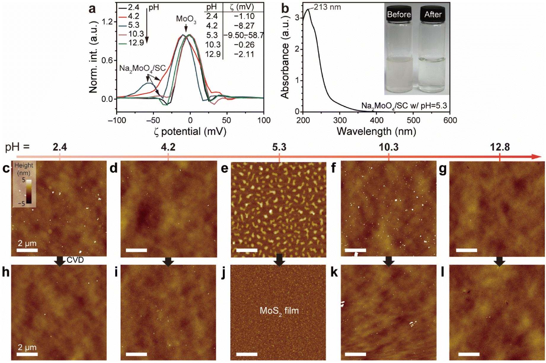 | ||
| Fig. 2 Impact of pH on spin-coated MoO3/SC adsorbates and subsequent MoS2 formation. (a) ζ-Potential measurements of MoO3/SC dispersions at varying pH levels (i.e., 2.4, 4.2, 5.3, 10.3, and 12.8). (b) The absorption spectrum of the filtered aqueous Na2MoO4/SC stock dispersion (black). Inset: photographs of before and after 0.2 μm filtration of the Na2MoO4/SC dispersion. (c–g) AFM topography images of Na2MoO4/SC spin-coated films at pH values of (c) 2.4, (d) 4.2, (e) 5.3, (f) 10.3, and (g) 12.8, with consistent height scales and scale bars. (h–l) The corresponding AFM images of the resulting MoS2 films grown via CVD sulfurization from each pH-controlled spin-coat. | ||
The inset of Fig. 2b shows a photograph of before and after the 0.2 μm filtration of the Na2MoO4/SC dispersion. The filtered sample is devoid of turbidity originating from MoO3. Fig. 2b displays the absorption spectrum of the filtered Na2MoO4/SC dispersion with pH ∼5.3. The Na2MoO4/SC dispersion exhibits a peak at 213 nm. The absorption bands between 200 and 400 nm correspond to ligand-to-metal charge transfer transitions (O2− → Mo6+),48 and the spectral shape aligns with that of Na2MoO4,49 in contrast to the broad visible-range absorption typically seen with MoO3.
AFM results of pH-controlled metal precursors and subsequent films support the pKa hypothesis. We investigated samples at various pH values (2.4, 4.2, 5.3, 10.3, and 12.8), taking into account the pKa values of molybdic acid, SC, and silanol moieties. The dispersions were spin-coated on the freshly O2-treated 285 nm thick SiO2/Si substrate while minimizing exposure to the atmosphere. Without the treatment, the sample failed to form a uniform MoS2 film despite both samples exhibiting similar surface morphologies and average surface roughness values (〈R〉 ≈ 0.2 nm) (see detailed characterization and a full explanation in Fig. S1a–S1g and Note S1†). Fig. 2c–g display AFM height images of the spin-coated Na2MoO4/SC dispersions at different pH levels. Notably, the spin-coat at pH 5.3 displays dense elongated droplet-like features with uniform height, whereas those at other pH levels display sporadic particle aggregates. This result correlates with the relative stability of the Na2MoO4/SC complex observed in the ζ-potential measurements. These findings align with the pKa hypothesis, where the mildly acidic dispersion (pH = 5.3) facilitates multiple hydrogen bonds with silanol groups while causing repulsion between metal precursors.
A similar trend is observed in the CVD-grown samples. CVD growth results in different films based on pH. Fig. 2h–l show AFM images of MoS2 films grown from dispersions at various pH values. Samples from pH 2.4, 4.2, 10.3, and 12.8 exhibit sporadic particle aggregates, while that from pH 5.3 yields a continuous MoS2 film from the previously discontinuous adsorbates, indicating MoS2 growth. As a result, the Na2MoO4/SC dispersion at pH 5.3 is used for further experiments. This control experiment demonstrates the effectiveness of the pH-controlled Na2MoO4/SC dispersion in achieving the formation of a continuous MoS2 film.
The transformation of organic dispersants, such as SC, during the growth process remains a subject of interest. Previous studies using in situ Raman spectroscopy and TEM coupled with energy-dispersive X-ray spectroscopy (EDS) have shown that amorphous carbon originating from SC begins to decompose around 500 °C.26 This decomposition is also likely linked to the sulfurization of Na2MoO4, which, during its conversion to MoS2, creates an in situ oxidative environment that promotes the breakdown of SC and removal of SC-derived amorphous carbon. Additionally, TEM-EDS analysis detected no remaining traces of amorphous carbon.26
Effect of precursor concentrations on MoS2 films
The reproducible and uniform spin-coating capability of the Na2MoO4/SC complex on a hydrophilic SiO2/Si substrate allowed for a quantitative study on the impact of the precursor concentration on the MoS2 film quality and layer number. To explore this, the 20 mM Na2MoO4/SC stock dispersion was diluted, and the corresponding MoS2 films were then prepared via the CVD process. Fig. 3a–d show AFM height images of spin-coated Na2MoO4/SC at different concentrations. The 4 mM sample does not exhibit any distinct features, and closely resembles the native morphology of the 285 nm thick SiO2/Si substrate (Fig. S1c†). However, samples at 6 mM and higher show noticeably elongated adsorbates with increasing heights and sizes. Height profiles in Fig. S2a† indicate that Na2MoO4/SC adsorbates reach heights up to 7 nm. Quantitative analysis (Fig. S2b†) reveals that as Na2MoO4/SC concentrations increase, the adsorbate density decreases, while the volume (V) of each individual adsorbate increases. This suggests that dilution can control the concentration of the precursor adsorbate on the substrate. | ||
| Fig. 3 Systematic changes in precursor and MoS2 morphologies with increasing Na2MoO4/SC concentrations. (a–d) AFM height images of adsorbates from spin-coated Na2MoO4/SC dispersions at concentrations of 4, 6, 8, and 10 mM. (e–h) The corresponding MoS2 films formed by CVD sulfurization of each spin-coated sample through the CVD process. (i) Composite AFM height image composed of four scratched MoS2 quarters, each representing a different Na2MoO4/SC concentration. (j) Average height profile trends of the spin-coats and the corresponding MoS2 films. Red lines denote linear regression fits. (k) Normalized Raman spectra of MoS2 samples, with an Si band at 520.9 cm−1 as a reference, at various Na2MoO4/SC concentrations. (l) Plot showing the positions and peak separations of E12g and A1g bands of MoS2 samples as a function of Na2MoO4/SC concentration. | ||
Fig. 3e–h show AFM topographies of the corresponding MoS2 films formed by CVD sulfurization of each sample followed by isopropanol washing. The MoS2 films are continuous across all samples. Upon closer inspection, varying heights are observed beneath the MoS2 films, as shown in Fig. S2c.† Since the samples were grown with a sodium catalyst, sodium is likely present underneath the MoS2 films, which is in line with the literature.50 After thoroughly washing the MoS2 surface with isopropanol to remove surface sodium, EDS (Fig. S3a–S3d†) confirms the presence of sodium underneath. Sodium is randomly distributed across the surface. Atomic composition analysis (Fig. S3e†) shows that the atomic percentages of Na, Mo, and S are 11.9, 40.4, and 47.7%, respectively. This result suggests that the MoS2 film not only contains sodium underneath the surface but also exhibits an imbalanced Mo/S stoichiometry, in line with the literature.25
XPS measurements show the chemical states of the elements present. Fig. S4a–S4d† display the survey and detailed spectra of S 2p, Mo 3d, and Na 1s (see Note S2† for a detailed explanation). In the S 2p region (Fig. S4b†), only the MoS2 film exhibits the characteristic spin–orbit doublet peaks—S 2p3/2 at 161.1 eV and S 2p1/2 at 162.2 eV—indicative of metal sulfide.37 Similarly, in the Mo 3d region (Fig. S4c†), only the MoS2 film shows the Mo4+ spin–orbit doublet, with 3d5/2 at 228.2 eV and 3d3/2 at 231.3 eV (3.1 eV separation), whereas the MoO3, Na2MoO4, and Na2MoO4/SC drop-cast samples display features corresponding to Mo(VI). In the Na 1s region (Fig. S4d†), the MoS2 film shows a neutral sodium signal at 1071.4 eV, while the other samples show red-shifted singlet peaks between 1070.2 and 1070.7 eV, consistent with the presence of neutral amorphous sodium as confirmed by TEM images and sodium diffraction patterns.26 Additionally, the drop-cast sample shows a blue-shifted peak at 1070.7 eV compared to the Na2MoO4 powder (1070.2 eV), which qualitatively aligns with observations from the spin-coated Na2MoO4.50
Fig. 3i presents a composite AFM height image composed of four scratched MoS2 film quarters from each concentration, showing step heights of approximately 0.7, 1.2, 1.9, and 2.2 nm. These correspond to near single-layer (SL), bi-layer (BL), tri-layer (TL), and multi-layer (ML) MoS2. A comparison of height trends (Fig. 3j) reveals a linear correlation between the average thicknesses of the spin-coated precursor layers and the resulting MoS2 films. The spin-coat thickness yspincoat varies linearly with concentration as yspincoat = 0.275x − 1.3, where x is the Na2MoO4/SC concentration. Similarly, the MoS2 film thickness yMoS2 follows the relation yMoS2 = 0.26x − 0.32. Combining these two expressions yields a direct correlation between the precursor layer and the film thickness as follows:
| yMoS2 = 0.945yspincoat − 0.91 nm | (1) |
This empirical eqn (1) provides a practical thickness conversion factor, useful for estimating and targeting the desired MoS2 film thickness.
Raman spectra of the MoS2 films, as shown in Fig. 3k, reveal systematic changes in the E12g and A1g bands with increasing Na2MoO4/SC concentrations. The interpeak separation and their intensities progressively increase as Na2MoO4/SC concentrations rise. The interpeak separation (Fig. 3l) for the 4 mM-derived sample shows 21.0 cm−1, while samples from 6 mM and higher show an increase in separation, reaching up to 24.2 cm−1, indicating a transition from BL to ML MoS2,32,51 in line with AFM results. This result demonstrates the ability to control the number of MoS2 layers by adjusting the precursor concentration.
This method enables the growth of continuous, large-area MoS2 films on a centimeter scale. Fig. 4a shows photographs of the fully grown continuous MoS2 on a 285 nm thick SiO2/Si substrate, both with and without masking. The left image shows the film without masking, while the right one shows the masked area, created using Denko tape during the spin-coating process to generate different contrasts in the exposed regions. The uniformity of the MoS2 film was confirmed by point Raman spectra taken across the sample. Raman spectra (Fig. 4b) exhibited consistent positions (i.e., ∼383.8 and ∼404.2 cm−1), interpeak separation (∼20.4 cm−1), and intensities, indicating a uniform MoS2 film. Fig. 4c shows an AFM image of the scratched MoS2 film, revealing a flat surface with an ∼0.6 nm-deep trench, confirming the formation of the SL MoS2 film.
 | ||
| Fig. 4 Continuous large-area polycrystalline FL MoS2. (a) Continuous large-area MoS2 (left) and continuous large-area MoS2 with a bare area generated using Denko tape during the spin-coating process (right). (b) Raman spectra taken across the entire MoS2 sample as indicated in (a). (c) AFM image of a scratched MoS2 film. (d) HAADF-STEM image of the polycrystalline MoS2 film showing sporadic Moiré patterns marked by white arrows. Inset: diffraction patterns displaying five distinct sets of hexagonal patterns. (e) Color-coded representation of MoS2 polycrystallites based on five crystal orientations, highlighting BL and TL regions with distinct Moiré patterns, as well as SL regions. (f) HAADF-STEM image showing grain boundaries with lined (6|4)–(7|5) defects. | ||
TEM analysis reveals the polycrystalline nature of the MoS2 film. Fig. 4d shows a high-angle annular dark-field scanning transmission electron microscopy (HAADF-STEM) image of the transferred MoS2 film. Upon closer examination, Moiré patterns35 (indicated by the white arrows) are observed, suggesting twisted BL MoS2 alongside the SL regions. The inset diffraction in Fig. 4d reveals five sets of hexagonal diffraction patterns corresponding to the 2H polymorph of MoS2. By masking other diffraction patterns and applying color-coding,22 polycrystalline MoS2 domains are revealed (Fig. 4e). This analysis shows that SL MoS2 is the predominant layer, with minor BL and TL regions. Fig. 4f presents an HAADF-STEM image of grain boundaries between SL–SL regions, highlighting their atomic reconstruction with connected (6|4)–(7|5) defects, which are common in MoS2.52,53
Real-time growth kinetics of the continuous MoS2 film
The growth kinetics leading to the continuous MoS2 film were analyzed through a real-time growth video captured using an ICVDM.26 To observe the growth kinetics, a MoS2 film with a bare area was grown, while the bare area was generated using Denko tape (right panel of Fig. 4a). This sample provides contrast (CR) values of the growing layer26,34,54 (see the Experimental section), and its growth trajectories were recorded and are presented in the ESI (Video S1†). The video shows that the precursor spin-coat gradually transforms into a MoS2 film without forming the typical triangular shape. This suggests that the growth occurs uniformly across the substrate, with crystallites smaller than the diffraction limit of the optical system (up to 660 nm, considering the numerical aperture (0.5) of the lens used in this experiment).Fig. 5a shows the CVD programming profile, including the CVD temperature (TCVD), sulfur temperature (TS), and argon flow (FAr) as a function of reaction time trxn. Real-time optical images corresponding to trxn are presented in Fig. 5b–d. At trxn = 30 s (or TCVD = 500 °C), the spin-coat begins to change color, in which the precursor spin-coat area does not display a large contrast compared to the bare area. However, at trxn = 90 s (or TCVD = 600 °C), the spin-coat rapidly changes color, with the interface showing a large contrast, indicating the formation of ML MoS2. At trxn = 4 min (or TCVD = 800 °C), the film's color reaches saturation. Fig. 5e presents the CR trends at various positions indicated in the optical images, depending on trxn and TCVD. The deformation of the spin-coat starts at TCVD = 500 °C, consistent with a prior study.26 Notably, unlike MoS2 growth at 350 °C using volatile and fragile molybdenumhexacarbonyl (Mo(CO)6) and hydrogen sulfide (H2S) via metal–organic CVD,55 the growth temperature for MoS2 using Na2MoO4 and sulfur as precursors can be reduced to as low as 500 °C. The CR analysis26 reveals that while position 1, located at the thick interface between the spin-coat and bare areas, forms ML MoS2, positions 2 and 3, which are farther from the interface and therefore thinner, show BL and SL regions. The absence of intermediate triangular or hexagonal shapes in optical observation indicates that the MoS2 film is composed of submicrometer-sized crystallites, which aligns with the TEM observations. Increasing the crystallite size would enhance the optoelectronic quality of the MoS2 film, a topic for future investigation.
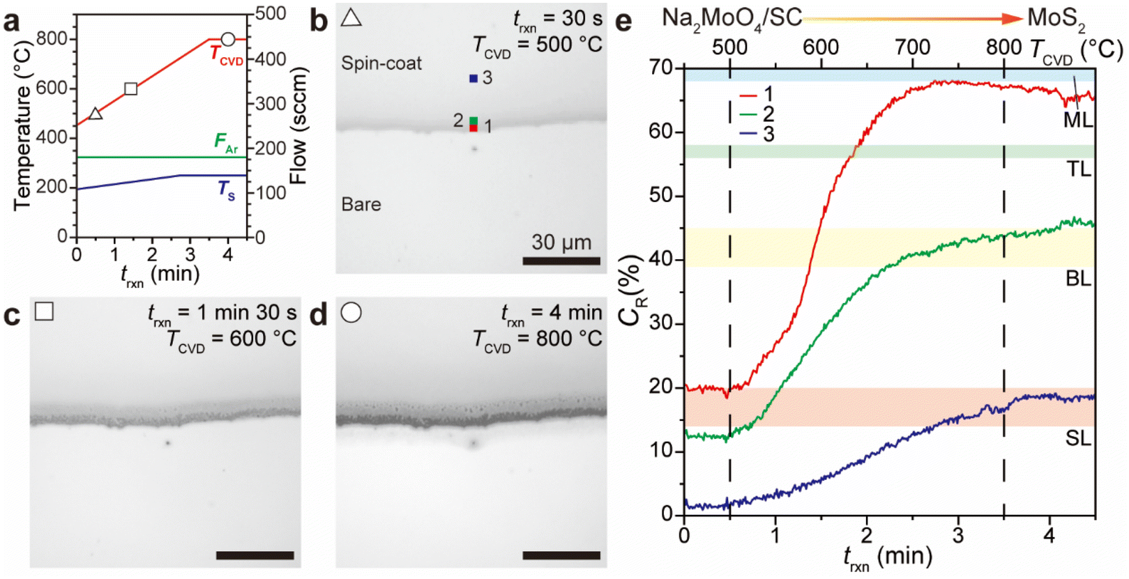 | ||
| Fig. 5 Growth kinetics of the continuous MoS2 film observed using an ICVDM. (a) Programming parameter (TCVD, TS, and FAr) profiles during the ICVDM reaction. Real-time optical images of the MoS2 film at trxn = (b) 30 s, (c) 1 min 30 s, and (d) 4 min. (e) CR trends of the positions in the optical images in (b) according to trxn and TCVD. | ||
The catalytic roles of sodium and SC were explored through several control experiments. The first experiment used MoO3 without SC, the second involved Na2MoO4 without SC, and the third used MoO3 with a different dispersant, such as SDS (see the Experimental section). The first experiment investigates the catalytic roles of sodium and SC, the second examines the role of SC, and the third explores the impact of SC's pKa. Similar ICVDM experiments, as shown in Fig. S5a–S5g, S6a–S6g, and S7a–S7g† (see Note S3† for full details), were conducted. Briefly, MoO3 spin-coating promotes MoS2 growth at the interface between the spin-coat and bare areas at prolonged trxn (∼10 min) at 800 °C (Fig. S5†). Na2MoO4 only leads to the formation of discontinuous, micrometer-sized ML grains at extended trxn (∼20 min) at 800 °C (Fig. S6†). Lastly, the MoO3/SDS case does not exhibit any MoS2 features except for the interface after 10 min trxn at 800 °C (Fig. S7†). SDS, with a low pKa (i.e., 2), is ineffective in producing MoS2. From these experiments, the sodium catalyst from SC can lower the reaction temperature, and an appropriate pKa value of the dispersant is an important aspect for continuous MoS2 growth.
Thus far, we have shown that optimizing the pH of the metal precursor buffer facilitates the growth of continuous MoS2 films. Additionally, we hypothesize that sodium content is another crucial factor influencing both the growth kinetics and the morphology of the films. Sodium particles that are optically visible promote the formation of ML MoS2, while those that are optically invisible favor the growth of SL MoS2.26 These sodium catalysts fragmented and moved along the edges, enhancing the MoS2 growth.26,28 Recent research indicates that sodium, decomposed from a Na2MoO4 precursor, accumulates at the interface between MoS2 and the SiO2 substrate, becoming embedded into the substrate over extended growth periods.50 This edge or interfacial sodium likely plays a significant role in influencing growth kinetics and morphology. Further investigation into this process will be an important direction for future research.
Conclusions
In this study, we achieved continuous, centimeter-scale MoS2 growth on a SiO2 surface using an SC-buffered, uniformly spin-coatable metal precursor via the CVD process. This method leverages a sodium molybdate/SC complex with pH = 5.3, based on the pKa values of the metal precursor, dispersant, and substrate. By systematically exploring sodium-based metal precursor dispersions, we presented a reproducible relationship between the precursor concentration and the number of MoS2 layers. By minimizing moisture exposure, we achieved robust, reproducible MoS2 growth with randomly oriented polycrystallites. Our findings demonstrate that the increased adsorbed concentration of metal precursors directly influences the increasing number of MoS2 layers, providing precise control over the resulting structures. These mildly acidic metal precursor dispersions support patterned continuous growth and are compatible with photolithography techniques for further device integration. An ICVDM allows us to observe the growth kinetics of continuous MoS2 according to the reaction time and furnace temperature, indicating that the growth occurs even at temperatures as low as 500 °C. Several control experiments investigating the roles of sodium, SC, and the pKa of SC further highlight the critical importance of the in situ formation of Na2MoO4 facilitated by SC. This simple spin-coating method provides a route to produce complex hierarchical TMC structures with high reproducibility, advancing the development of optoelectronic devices.Author contributions
D. H. Kim performed the experiments, characterized the samples, and analyzed the data. J. Seo and Y. Kang performed the experiments. B. Lee performed the experiments and analyzed the data. S.-Y. Ju conceived the idea and supervised the project. S.-Y. Ju wrote the manuscript. All the images/artwork/photos that appear in the manuscript and ESI† were created by the authors of this manuscript.Data availability
The data supporting this article have been included as part of the ESI.†Conflicts of interest
We have filed a Korean Patent (filing date: 2024.11.19, filing number: 10-2024-0165414) regarding pH-optimized metal precursor dispersion for CVD growth of TMCs.Acknowledgements
This research was supported financially by YU-KRISS (KRISS-GP2024-0012-GONG9), and in part by the Basic Science Research Program (NRF-2022R1A2C1006932) through the National Research Foundation of Korea (NRF) funded by the Ministry of Education, Science, and Technology.References
- A. Splendiani, L. Sun, Y. Zhang, T. Li, J. Kim, C.-Y. Chim, G. Galli and F. Wang, Nano Lett., 2010, 10, 1271–1275 CrossRef CAS PubMed.
- B. Radisavljevic, A. Radenovic, J. Brivio, V. Giacometti and A. Kis, Nat. Nanotechnol., 2011, 6, 147–150 CrossRef CAS PubMed.
- Y.-H. Lee, L. Yu, H. Wang, W. Fang, X. Ling and Y. Shi, et al., Nano Lett., 2013, 13, 1852–1857 CrossRef CAS PubMed.
- A. Castellanos-Gomez, M. Buscema, R. Molenaar, V. Singh, L. Janssen, H. S. J. van der Zant and G. A. Steele, 2D Mater., 2014, 1, 011002 CrossRef CAS.
- P. Rivera, K. L. Seyler, H. Yu, J. R. Schaibley, J. Yan, D. G. Mandrus, W. Yao and X. Xu, Science, 2016, 351, 688–691 CrossRef CAS PubMed.
- K. Kang, K.-H. Lee, Y. Han, H. Gao, S. Xie, D. A. Muller and J. Park, Nature, 2017, 550, 229–233 CrossRef PubMed.
- Y. Meng, T. Wang, C. Jin, Z. Li, S. Miao and Z. Lian, et al., Nat. Commun., 2020, 11, 2640 CrossRef CAS PubMed.
- R. Rosati, I. Paradisanos, L. Huang, Z. Gan, A. George and K. Watanabe, et al., Nat. Commun., 2023, 14, 2438 CrossRef CAS PubMed.
- Z. Yin, H. Li, H. Li, L. Jiang, Y. Shi and Y. Sun, et al., ACS Nano, 2012, 6, 74–80 CrossRef CAS PubMed.
- J. S. Kim, H. S. Lee, P. J. Jeon, Y. T. Lee, W. Yoon, S.-Y. Ju and S. Im, Small, 2014, 10, 4845–4850 CrossRef CAS PubMed.
- V. K. Kumar, S. Rathkanthiwar, A. Rao, P. Ghosh, S. Dhar, H. Chandrasekar, T. Choudhury, S. A. Shivashankar and S. Raghavan, ACS Appl. Nano Mater., 2021, 4, 6734–6744 CrossRef CAS.
- H. Choi, B. H. Moon, J. H. Kim, S. J. Yun, G. H. Han, S.-g. Lee, H. Z. Gul and Y. H. Lee, ACS Nano, 2019, 13, 13169–13175 CrossRef CAS PubMed.
- Z. Y. Zhu, Y. C. Cheng and U. Schwingenschlögl, Phys. Rev. B: Condens. Matter Mater. Phys., 2011, 84, 153402 CrossRef.
- K. F. Mak, K. He, J. Shan and T. F. Heinz, Nat. Nanotechnol., 2012, 7, 494–498 CrossRef CAS PubMed.
- K. F. Mak, K. L. McGill, J. Park and P. L. McEuen, Science, 2014, 344, 1489–1492 CrossRef CAS PubMed.
- H. Yuan, X. Wang, B. Lian, H. Zhang, X. Fang and B. Shen, et al., Nat. Nanotechnol., 2014, 9, 851–857 CrossRef CAS PubMed.
- N. Zibouche, P. Philipsen, A. Kuc and T. Heine, Phys. Rev. B: Condens. Matter Mater. Phys., 2014, 90, 125440 CrossRef.
- Z. Li, X. Meng and Z. Zhang, J. Photochem. Photobiol., C, 2018, 35, 39–55 CrossRef CAS.
- Y. Luo, K. Ren, S. Wang, J.-P. Chou, J. Yu, Z. Sun and M. Sun, J. Phys. Chem. C, 2019, 123, 22742–22751 CrossRef CAS.
- A. M. van der Zande, P. Y. Huang, D. A. Chenet, T. C. Berkelbach, Y. You and G.-H. Lee, et al., Nat. Mater., 2013, 12, 554–561 CrossRef CAS PubMed.
- S. Wang, Y. Rong, Y. Fan, M. Pacios, H. Bhaskaran, K. He and J. H. Warner, Chem. Mater., 2014, 26, 6371–6379 CrossRef CAS.
- K. Kang, S. Xie, L. Huang, Y. Han, P. Y. Huang, K. F. Mak, C.-J. Kim, D. Muller and J. Park, Nature, 2015, 520, 656–660 CrossRef CAS PubMed.
- G. H. Han, N. J. Kybert, C. H. Naylor, B. S. Lee, J. Ping and J. H. Park, et al., Nat. Commun., 2015, 6, 6128 CrossRef CAS PubMed.
- S. Li, Y.-C. Lin, W. Zhao, J. Wu, Z. Wang and Z. Hu, et al., Nat. Mater., 2018, 17, 535–542 CrossRef CAS PubMed.
- S. Li, Y.-C. Lin, X.-Y. Liu, Z. Hu, J. Wu and H. Nakajima, et al., Nanoscale, 2019, 11, 16122–16129 RSC.
- J. Oh, M. Park, Y. Kang and S.-Y. Ju, ACS Nano, 2024, 18, 19314–19323 CrossRef CAS PubMed.
- J. Zhou, J. Lin, X. Huang, Y. Zhou, Y. Chen and J. Xia, et al., Nature, 2018, 556, 355–359 CrossRef CAS PubMed.
- L. Huang, Q. H. Thi, F. Zheng, X. Chen, Y. W. Chu, C.-S. Lee, J. Zhao and T. H. Ly, J. Am. Chem. Soc., 2020, 142, 13130–13135 CrossRef CAS PubMed.
- H. Wang, X. Zhu, Z. Zhao, X. Wang, Z. Qian and L. Jiao, et al., Nano Lett., 2024, 24, 5498–5505 CrossRef CAS PubMed.
- E. Koo, Y. Lee, Y. Song, M. Park and S.-Y. Ju, ACS Appl. Electron. Mater., 2019, 1, 113–121 CrossRef CAS.
- Y. Song, M. Park, J. Park, H. S. Ahn, T. K. Kim and S.-Y. Ju, Nanomaterials, 2022, 12, 1706 CrossRef CAS PubMed.
- J. Park, S. Bong, J. Park, E. Lee and S.-Y. Ju, ACS Appl. Mater. Interfaces, 2022, 14, 50308–50317 CrossRef CAS PubMed.
- S. Hong, M. Park, S. Kwon, J. Oh, S. Bong, B. Krishnakumar and S.-Y. Ju, Carbon, 2021, 183, 84–92 CrossRef CAS.
- E. Koo and S.-Y. Ju, Carbon, 2015, 86, 318–324 CrossRef CAS.
- E. Koo, S. Kim and S.-Y. Ju, Carbon, 2017, 111, 238–247 CrossRef CAS.
- J. Park, Y. R. Han, M. Park, C.-H. Jun and S.-Y. Ju, Carbon, 2020, 161, 599–611 CrossRef CAS.
- M. Jeong, S. Kim and S.-Y. Ju, RSC Adv., 2016, 6, 36248–36255 RSC.
- L. Chen, X. He, H. Liu, L. Qian and S. H. Kim, J. Phys. Chem. C, 2018, 122, 11385–11391 CrossRef CAS.
- S. Bong, S. Hwang and S.-Y. Ju, J. Phys. Chem. C, 2024, 128, 11229–11238 CrossRef CAS.
- Technical Data Sheet: Sodium Molybdate Dihydrate, https://northmetal.net/wp-content/uploads/Sodium-Molybdate-Dihydrate-Sodium-Molybdate-SMX-Na2MoO4-H2O-NaMoO4-10102-40-6-TDS-2.pdf, accessed 2025.03.20.
- D. J. Belton, O. Deschaume and C. C. Perry, FEBS J., 2012, 279, 1710–1720 CrossRef CAS PubMed.
- S. Asbrink, L. Kihlborg and M. Malinowski, J. Appl. Crystallogr., 1988, 21, 960–962 CrossRef CAS.
- T. P. Dadze, G. A. Kashirtseva, M. P. Novikov and A. V. Plyasunov, Fluid Phase Equilib., 2017, 440, 64–76 CrossRef CAS.
- W. L. Lindsay and K. M. Catlett, in Future Prospects for Soil Chemistry, ed. P. M. Huang, 1998, pp. 123–138 Search PubMed.
- J. J. Cruywagen, in Advances in Inorganic Chemistry, ed. A. G. Sykes, Academic Press, 1999, vol. 49, pp. 127–182 Search PubMed.
- Z. Minubayeva and T. M. Seward, Geochim. Cosmochim. Acta, 2010, 74, 4365–4374 CrossRef CAS.
- D. J. Cabral, J. A. Hamilton and D. M. Small, J. Lipid Res., 1987, 27, 334–343 CrossRef.
- R. K. Rana and B. Viswanathan, Catal. Lett., 1998, 52, 25–29 CrossRef CAS.
- O. G. Abdullah, S. B. Aziz, D. R. Saber, R. M. Abdullah, R. R. Hanna and S. R. Saeed, J. Mater. Sci.: Mater. Electron., 2017, 28, 8928–8936 CrossRef CAS.
- R. A. Kalt, A. Arcifa, C. Wäckerlin and A. Stemmer, Nanoscale, 2023, 15, 18871–18882 RSC.
- C. Lee, H. Yan, L. E. Brus, T. F. Heinz, J. Hone and S. Ryu, ACS Nano, 2010, 4, 2695–2700 CrossRef CAS PubMed.
- W. Zhou, X. Zou, S. Najmaei, Z. Liu, Y. Shi and J. Kong, et al., Nano Lett., 2013, 13, 2615–2622 CrossRef CAS PubMed.
- N. Gao, Y. Guo, S. Zhou, Y. Bai and J. Zhao, J. Phys. Chem. C, 2017, 121, 12261–12269 CrossRef CAS.
- H. Zhang, Y. Ma, Y. Wan, X. Rong, Z. Xie, W. Wang and L. Dai, Sci. Rep., 2015, 5, 8440 CrossRef CAS PubMed.
- J. Mun, Y. Kim, I.-S. Kang, S. K. Lim, S. J. Lee, J. W. Kim, H. M. Park, T. Kim and S.-W. Kang, Sci. Rep., 2016, 6, 21854 CrossRef CAS PubMed.
Footnotes |
| † Electronic supplementary information (ESI) available. See DOI: https://doi.org/10.1039/d5nr01193k |
| ‡ These authors contributed equally to this work. |
| This journal is © The Royal Society of Chemistry 2025 |