
 Open Access Article
 This Open Access Article is licensed under a
 Creative Commons Attribution 3.0 Unported Licence
A multilayer template stripping transfer printing method for engineered stretchable electronics†
Léo
Sifringer
 ,
Daniel
Laguna
,
Michel
Sommer
and
János
Vörös
*
,
Daniel
Laguna
,
Michel
Sommer
and
János
Vörös
*
Laboratory of Biosensors and Bioelectronics, ETH Zürich, Gloriastrasse 37/39, Zürich, Switzerland. E-mail: janos.voros@biomed.ee.ethz.ch
First published on 30th May 2025
Abstract
Stretchable electronics require sophisticated fabrication strategies to achieve both high electrical performance and mechanical compliance. While various approaches exist, from geometric designs to composite materials, most face challenges in balancing fabrication complexity with device performance. Here, we present a multilayer template stripping approach for fabricating stretchable conductors. This method combines the precision and scalability of template-based fabrication with the simplicity of transfer printing to create engineered microwire networks. Through systematic investigation of geometric parameters, we establish design rules for optimizing mechanical resilience of microwire arrays. We demonstrate both high-performance designs achieving 100% stretchability and robust architectures tolerant to fabrication variations, while maintaining low electrical resistance. The process is compatible with various metals and enables rapid, large-area fabrication, offering a practical route toward scalable manufacturing of stretchable conductors.
1 Introduction
The development of stretchable electronics is essential for advancing wearable healthcare and biomedical devices.1,2 While significant progress has been made in materials and designs for stretchable conductors, scalable and versatile fabrication routes remain a key challenge for widespread adoption.3–5 Current approaches often require complex processing steps and specialized equipment,5,6 or face fundamental limitations in scalability and manufacturability.7–9 Several distinct strategies can be used to create stretchable conductors, which can usually be classified into five distinct categories: microcracked films,10 patterned interconnects,11–13 intrinsically conductive polymers,14,15 liquid metals,16 and stretchable composites.17,18 Microcracked metal films make use of controlled crack formation in thin metal films on elastomeric substrates enabling stretchability while maintaining electrical conductivity.19–21 However, achieving reliable and reproducible crack patterns remains challenging,22,23 rendering their stretchability limited. Geometrically designed structures, such as serpentine, fractal or kirigami patterns effectively redistribute strain through out-of-plane deformation, enabling high stretchability.24–26 While powerful, this approach faces fundamental limitations in miniaturization, as the mechanical advantages diminish at smaller scales.27 Additionally, achieving high-density features while maintaining stretchability presents significant design and fabrication challenges.28 Liquid metals, primarily based on gallium alloys, offer intrinsic deformability while maintaining metallic conductivity.16 Recent developments have improved patterning capabilities29 and enabled higher resolution features.30 Nevertheless, these materials face ongoing challenges in biocompatibility and long-term stability,16 particularly for biomedical applications.31 Organic conductors, such as PEDOT![[thin space (1/6-em)]](https://www.rsc.org/images/entities/char_2009.gif) :PSS and its derivatives, provide another materials-based solution.32 While offering intrinsic deformability and compatibility with solution processing,33 these materials typically exhibit lower conductivity compared to metallic conductors,34 and often face stability issues in ambient conditions for biomedical applications.35 Stretchable composites use nanomaterials such as nanowires,36,37 or nanoparticles38 as filler in a stretchable matrix, and have demonstrated impressive combinations of electrical and mechanical properties.39–41 However, the fabrication process often involves complex synthesis protocols41,42 and challenges in achieving uniform assembly over large areas,43 limiting scalability.
:PSS and its derivatives, provide another materials-based solution.32 While offering intrinsic deformability and compatibility with solution processing,33 these materials typically exhibit lower conductivity compared to metallic conductors,34 and often face stability issues in ambient conditions for biomedical applications.35 Stretchable composites use nanomaterials such as nanowires,36,37 or nanoparticles38 as filler in a stretchable matrix, and have demonstrated impressive combinations of electrical and mechanical properties.39–41 However, the fabrication process often involves complex synthesis protocols41,42 and challenges in achieving uniform assembly over large areas,43 limiting scalability.
Despite these advances, a critical need remains for fabrication approaches that combine simplicity, versatility, and scalability while maintaining good electrical and mechanical performance. Micro- and nanotransfer-based processes have been shown to enable the assembly of complex electronic systems with high fidelity and minimal defects, which is critical for ensuring the performance and reliability of stretchable devices.44 The scalability of fabrication processes based on micro and nano transfer techniques7,45 is another significant advantage. Traditional methods for fabricating stretchable electronics often involve labor-intensive and time-consuming processes that limit their applicability in mass production scenarios. In contrast, transfer printing techniques can be adapted for high-throughput manufacturing, allowing for the rapid production of large-area stretchable electronics. Unlike ink printing methods which utilize functional materials in solution form (e.g., graphene inks46), our template-based transfer approach directly patterns solid metal layers, offering higher conductivity and precise feature control at the micro- to nanoscale while maintaining the processability advantages of printing-based fabrication. However, most transfer-based approaches focus on single-layer materials, such as patterned organic or inorganic conductors, and thus face similar material-specific limitations. Building upon an established template stripping method,47 we present a multilayer approach that uses sequential transfers to create engineered wire networks. This process combines the scalability of transfer printing with the mechanical advantages of wire architectures, while avoiding the complex synthesis and assembly challenges of conventional nanowire-based methods. The approach is compatible with various materials, requires minimal specialized equipment, and can be completed rapidly compared to conventional fabrication routes. The resulting conductors demonstrate good mechanical performance, offering a practical balance between fabrication simplicity and device performance. This new fabrication strategy for stretchable conductors is based on multilayer template stripping that is fundamentally different from existing approaches that typically rely on single-layer transfer or complex material synthesis. We show that sequential transfers can create engineered microwire networks with controlled geometry and connectivity with unprecedented precision, since the layout geometry is controlled lithographically on the silicon template. This concept bridges the gap between geometric design approaches and nanomaterial-based methods by enabling precise control over microwire arrangements while maintaining fabrication simplicity. By leveraging template reusability and straightforward transfer processes, our approach provides an accessible route to stretchable conductor fabrication without compromising device performance or scalability, since no lithography steps are needed after the initial template fabrication. This strategy opens new opportunities for implementing stretchable electronics in practical applications by addressing key manufacturing challenges while maintaining device performance.
2 Results and discussion
2.1 A multilayer template-stripping based transfer printing
The fabrication process comprises several key steps, as illustrated in Fig. 1A (detailed procedures are provided in the Experimental section). The process begins with the creation of a template through patterning and dry etching of a silicon wafer, followed by metal (typically Au) evaporation. A flexible adhesive-supported polyvinyl alcohol (PVA) layer is used to strip the top metal layer from the template through soft lamination. The pressure-less nature of this lamination ensures selective stripping of metal only from the template's top surface, despite the adhesive sheet's flexibility. By performing this process at 120 °C, above PVA's glass transition temperature, the adhesion strength to Au is enhanced. Upon cooling to room temperature, the sheets are separated, enabling reliable pattern transfer at both nano- and microscales.47 The metal pattern is subsequently transferred onto a stretchable polydimethylsiloxane (PDMS) substrate through pressure lamination at 120 °C, followed by pressure using a soft stamp for at least 30 seconds. The lamination and stripping processes are carried out manually. After separating the supporting layer, the PVA is dissolved in water. While this dissolution can occur at room temperature, using boiling water accelerates the process to approximately 10 minutes due to PVA's enhanced dissolution rate above 80 °C. This entire process can be repeated to stack multiple layers of patterned metal on the receiving substrate, with an additional PDMS layer spin-coated onto the transferred metal layers for encapsulation. This methodology enables the creation of stretchable interconnects, as demonstrated in Fig. 1B. Fig. 1C reveals the hierarchical structure, where two arrays of microwires are pictured – one array with microwires extending from bottom left to top right (first layer), and another from bottom right to top left (second layer). The process offers several distinct advantages. First, pattern geometry is defined by the metal-coated template, which can be fabricated from various materials (e.g., silicon or SU-8) using any established lithographic method. Second, successful transfer relies on the differential adhesion between the metal-template and metal-PVA interfaces. When necessary, an optional perfluoro-silane treatment can be introduced between template fabrication and metal evaporation to reduce template adhesion, enabling transfer of materials that typically exhibit strong template adhesion. This versatility has been demonstrated in the successful transfer and plasma bonding of SiO2/Ti/Pt stacks for soft multi-electrode arrays.48 Since the Young modulus of PDMS can be tailored within a wide range,49 the mechanical properties of the substrate could be tuned for different applications if needed. Finally, as shown in Fig. 1A, the template can be reused following wet etching of residual metal, enabling a highly efficient and straightforward fabrication process. The ability to precisely control pattern geometry through template design, combined with the capability for multilayer stacking, provides unique opportunities for creating stretchable conductors. However, successful implementation of this approach requires detailed understanding of how geometric parameters affect mechanical performance, as well as careful consideration of layer-to-layer alignment during the transfer process. These factors guided our subsequent investigation of microwire array mechanics and informed the development of practical design strategies. | ||
| Fig. 1 (A) Fabrication process flow for multilayer template stripping transfer printing: first, a template is created by dry etching a patterned silicon wafer, and metal is evaporated onto it. A PVA thin film, backed by a PEN foil, is laminated onto the template and peeled off to pick the top layer of patterned metal. This patterned metal can be then transferred on a PDMS substrate, and PVA dissolved in water. This transfer step can be done several times in a row to stack patterned metal onto the receiving substrate. Lastly, PDMS is spin-coated for encapsulation. (B) Photographs of a stretchable interconnect fabricated using this process flow with 2 layers. (C) Microscope image of the microstructure of the interconnect, revealing 2 layers of microwires (one layer with wires oriented diagonally bottom left-top right, and another layer with wires oriented diagonally bottom right-top left). | ||
2.2 Characterization of transferred microwires upon mechanical strain
To develop geometries suitable for stretchable electronics, we first investigated how different design parameters affect the mechanical resilience of single-layer arrays of microwires transferred onto PDMS. We began by examining the influence of microwire orientation relative to the direction of strain using Finite Element Analysis (FEA). As shown in Fig. 2A, microwires aligned more closely with the direction of strain (smaller angles) experience higher stress compared to those oriented more perpendicularly (larger angles). The von Mises stress was used as an indicator of microwire failure. | ||
| Fig. 2 (A) FEA results of wires with different orientations when subjected to 40% strain. The colors in the wires represent the experienced von Mises stress. (B) Process flow used for the mechanical characterization of wires subjected to strain. (i) Example of a pristine wire at rest, (ii) wire experiencing strain and breaking as a result thereof, (iii) the processed image reveals the detection of 2 distinct segments, confirming the cracking of the wire. (C) Average number of cracks per wire for each angle group, as a function of strain. Data points were taken every 5% strain. N = 5 to 18, depending on how many wires would fit in the field of view for a given angle and strain. (D) The critical strain at which each microwire first breaks, across all orientations. Each scattered dot represents a single wire breaking, and the violin plot shows the distribution. Since photographs were taken every 5% only, the dots are placed in the middle of the interval between the last strain without breakage and the interval at which breakage was noted, with an artificial jitter for visualization. Angles from 70° to 90° are not presented as no cracks were seen. Statistical significance was determined using Kruskal–Wallis test with Dunn's post hoc test (***p < 0.001). | ||
To validate these computational predictions, we conducted experimental studies by gradually stretching microwire arrays under microscopic observation at regular intervals (representative images in Fig. S1A and Fig. S1B†). The images taken can then be processed and analyzed to reveal microwire fracture patterns, as illustrated in Fig. 2Bi (before fracture), Fig. 2Bii (after fracture), and Fig. 2Biii (processed image showing two distinct segments). The average number of cracks per microwire versus applied strain was quantified for different microwire orientations (Fig. 2C). Consistent with FEA predictions, microwire groups at smaller angles exhibited earlier and more frequent breakage. Fig. S1D† compares the simulated maximum stress for each group against strain, with overlaid experimental first-break points from Fig. 2C indicating ultimate tensile stress values between approximately 90 and 230 MPa. While ultimate tensile stress in thin films depends on multiple parameters including deposition conditions, grain size, and annealing, these values align with existing literature.50–53 The critical strain at first microwire breakage across all orientations is presented in Fig. 2D, confirming that microwires at larger angles withstand substantially higher strains before failure. The complete transition from intact to broken microwires for all groups is documented in Fig. S1C.†
We next investigated the influence of the microwires’ length, width, and spacing (both in length and width directions). Fig. 3A illustrates a typical microwire array with defined geometric parameters. In these investigations, we systematically varied one parameter while maintaining the others constant, employing both FEA (Fig. S2A†) and microscopic analysis (Fig. S2B and Fig. S2C†). Clear trends emerged: shorter microwires demonstrated superior strain tolerance (Fig. 3B, C, and Fig. S3A†), as did wider microwires (Fig. 3D, E and Fig. S3C†). These experimental observations were corroborated by FEA analysis (Fig. S3B and Fig. S3D†). Ultimate tensile strength values ranged between 380–550 MPa for the length study and 250–305 MPa for the width study.
 | ||
| Fig. 3 (A) Example of a microwire array used for the parameter study. The gray arrows denote the strain direction. The four parameters (width, length, spacing width-wise and spacing length-wise) are described on the photograph. For each parameter study, one parameter was swept while the others were kept constant. (B) Average crack per wire for each length, as a function of strain. (C) The critical strain at which each microwire first breaks, across all lengths. (D) Average crack per wire for each width, as a function of strain. (E) The critical strain at which each microwire first breaks, across all widths. (F) Average crack per wire for each spacing length-wise, as a function of strain. (G) The critical strain at which each microwire first breaks, across spacings length-wise. (H) Average crack per wire for each spacing width-wise, as a function of strain. (I) The critical strain at which each microwire first breaks, across spacings width-wise. Data points were taken every 4% strain. Each scattered dot in (C), (E), (G), and (I) represents a single wire breaking, and the violin plot shows the distribution. Since photographs were taken every 4% only, the dots are placed in the middle of the interval between the last strain without breakage and the interval at which breakage was noted, with an artificial jitter for visualization. For (B) N = 40 to 85 depending on how many wires would fit in the field of view at a given length and strain, for (D) N = 40 to 50, for (F) N = 25 to 50, for (H) N = 20 to 40. Statistical significance was determined using Kruskal–Wallis test with Dunn's post hoc test (*p < 0.05, **p < 0.01, ***p < 0.001). | ||
Wire spacing in both directions influenced mechanical performance. In the direction of strain (length-wise), increased spacing proved beneficial, with more widely separated microwires exhibiting both fewer cracks and delayed crack initiation (Fig. 3F, G and Fig. S4A†). Perpendicular to the direction of strain (width-wise), the opposite trend emerged: decreased spacing enhanced performance, with more closely packed microwires demonstrating reduced and delayed cracking (Fig. 3H, I and Fig. S4D†). FEA simulations for length-wise spacing aligned well with experimental results (Fig. S4E†), yielding ultimate tensile stress values between 300–460 MPa. However, the width-wise spacing simulations revealed more complex behavior. While the maximum stress analysis suggested better performance with wider spacing (Fig. S4B†), a comprehensive examination of all microwires in each group (Fig. S4C†) revealed a nuanced pattern: samples with smaller spacing began failing earlier, but those with larger spacing showed a more rapid transition from fully intact to fully broken states. This apparent discrepancy between maximum stress predictions and experimental observations suggests that the current model may require refinement to fully capture the complex mechanical interactions in closely packed microwire arrays. In this study, we aim to demonstrate the feasibility of creating stretchable electronics using our fabrication method. Thus, the FEA and the validation with experimental results shown in Fig. 2 and 3 serve to understand parameter influences and design rules. A more comprehensive mechanical and electrical study with more complex deformations, reflecting real life use cases, would be needed to showcase usefulness in biomedical applications.
2.3 Design of a highly stretchable geometry
The parametric analysis provided clear design guidelines for optimizing microwire arrays. We applied these insights to develop two complementary multilayer designs: a high-performance herringbone pattern that maximizes stretchability, and a more robust periodic architecture that balances mechanical performance with manufacturing considerations. A herringbone pattern emerged as a natural choice for a two-layer geometry, as illustrated in Fig. 4A. The design synthesis incorporated our single-layer analysis results, suggesting optimal parameters of wide microwires, short lengths, increased spacing in the direction of strain, decreased spacing perpendicular to strain, and angles of 70° or greater relative to the direction of strain. However, practical design constraints necessitated certain compromises: maintaining a sufficient length-to-width ratio to preserve microwire-like geometry, and ensuring adequate overlap between layers for both feasible alignment and robust electrical connectivity. The latter is particularly important as increased overlap creates redundant electrical pathways, potentially improving resilience against microwire failure. Based on these considerations, we selected the following parameters: 100 μm length, 4 μm width, 15 μm length-wise spacing, 25 μm width-wise spacing, and 70° angle, with each microwire overlapping two microwires of the opposing layer at each end. Fig. 4B shows the change of resistance of a 5 mm wide, 8 mm long sample with an initial sheet resistance of 8.3 Ω sq−1 and conductivity of 6000 S cm−1, a value in the same order of magnitude as other published fabrication methods.54 Remarkably, this geometry maintains performance beyond 100% strain with resistance increase (R/R0) remaining below 3 until approximately 80% strain. Interestingly, while our design and random nanowire networks both reach similar R/R0 values at 100% strain,55 our approach shows a much slower initial change of resistance. While specialized high-aspect-ratio serpentine structures56 and advanced silver nanowire composites57 can achieve better electrical stability under strain with a lower resistance change rate over a similar range of strain, our approach significantly outperforms many conventional screen-printed58 and inkjet-printed conductors.59 Though not achieving best-in-class performance, these results are promising and could be further improved through computational modeling and simulation studies to fine-tune the design parameters.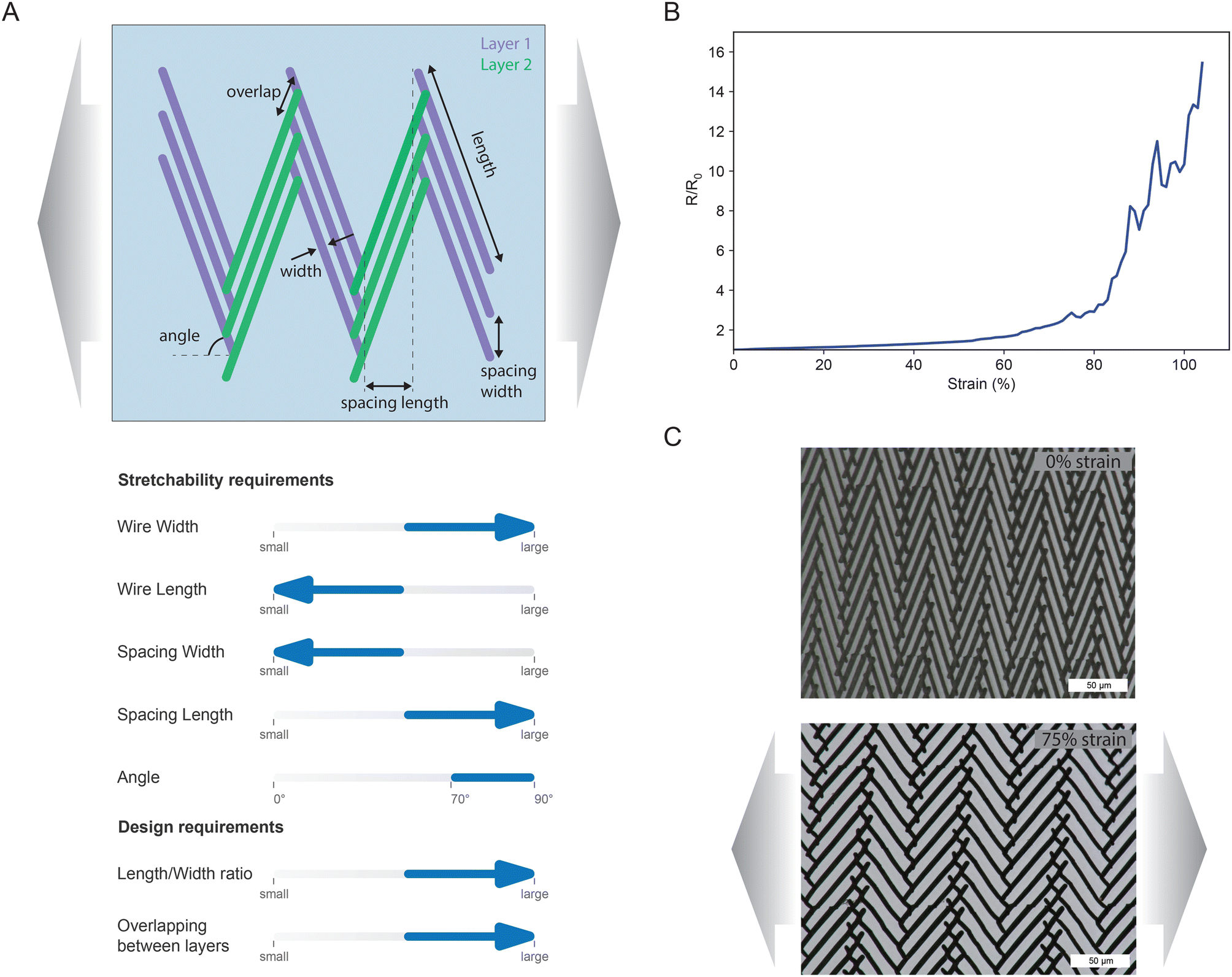 | ||
| Fig. 4 (A) Schematic of the herringbone 2-layer design with one layer depicted in purple and one in green. The gray arrows denote the strain direction. The requirements for high stretchability derived from the mechanical characterization of arrays of microwires are presented graphically, along with the requirements driven by practical design constraints. (B) Change of resistance of a herringbone sample when subjected to uniaxial strain. (C) Representative micrographs of the microstructure of a herringbone sample at 0% and 75% strain. | ||
Microscope pictures taken under strain show that microwires first undergo a sliding rotation (Fig. 4C), before starting to break at the overlap areas between microwires (hinge areas) (Fig. S5B†) at higher strains. FEA analysis (Fig. S5A†) confirmed maximum stress concentration at these hinge points. Our current hypothesis is that the minimal initial resistance change results from contact sliding and deformation, while the sharp increase beyond 80% strain reflects progressive microwire breakage, which reduces the number of available electrical pathways through the sample.
2.4 Design of a robust stretchable geometry
While the herringbone design achieves excellent stretchability, its reliance on precise layer-to-layer alignment across large areas poses a significant manufacturing challenge, with misalignment often resulting in non-conductive samples (Fig. S6†). To address this limitation, we developed a more robust design, presented in Fig. 5Ai. The layout partially relaxes some stretchability requirements discussed above in favor of a periodic pattern which ensures that misalignment does not result in a complete loss of conductivity (Fig. 5Aii). Additionally, the design incorporates redundant layer overlaps, where each microwire connects with multiple microwires in the opposing layer (the intersections are highlighted in red on the schematic), ensuring conductivity preservation even with imperfect transfer processes (Fig. 5Aiii). Doing so, this design leverages a fundamental property of wire networks, where contact points between conductors are essential for maintaining electrical pathways.55,60 Our periodic layout ensures that sufficient contact points between layers are preserved even under non-ideal conditions. Representative examples of misalignment and combined misalignment with imperfect transfer are shown in Fig. 5Aiv and Fig. 5Av, respectively. A typical sample used for tensile testing is shown in Fig. S7.† Performance characterization of three samples (600 μm width, 19 mm length, sheet resistance 32.5 ± 1.8 Ω sq−1) under uniaxial strain is presented in Fig. 5B. Although the strain-to-failure is lower than with the herringbone design, the relative resistance change remains well below 2 throughout the operating range. With sub-millimeter width and potential for further optimization and miniaturization, this design offers a straightforward path to fabricating stretchable interconnects. Notably, these samples demonstrate excellent durability, maintaining conductivity through over 1000 cycles at 50% strain (Fig. 5C). | ||
| Fig. 5 (A) Schematic of the so-called “robust” design. (i) Represents the ideal case were both layers are perfectly transferred and aligned. In the zoom-in, the red dots denote the contact points between layers. Their density is representative of the conductivity of a sample. (ii) In case of misalignment, there are less contact points but the design is still able to conduct electricity; (iii) similar behavior in case of imperfect transfer. (iv) shows micrographs of samples with misaligned layers, while and (v) depicts misaligned layers with imperfect transfer. (B) Change of resistance of samples when subjected to uniaxial strain (N = 3). The thick red line is the mean, the shaded red area is the standard deviation, and the dashed black lines are the individual samples. (C) Cyclic testing of a sample. In the blue shaded area, the sample was subject to strain between 0 and 33% strain, and in the red area between 33 and 50% strain. The insets are zoom-ins to depict the behavior of a few cycles. | ||
3 Conclusions
In summary, we have developed a multilayer template stripping approach that addresses key challenges in fabricating stretchable conductors. The systematic investigation of geometric parameters provided clear design guidelines for optimizing microwire arrays, enabling both high-performance and robust designs. The herringbone pattern demonstrates exceptional stretchability while maintaining conductivity, and the periodic design offers manufacturing tolerance without sacrificing electrical performance. The approach is compatible with various materials. We successfully transferred Au and Pt films evaporated on a bare, patterned, silicon template, as well as a SiO2/Ti/Pt stack evaporated on a silanized silicon template. Thicknesses of 100 nm and less were successfully transferred, while thicker evaporated thin films (200 nm) would suffer from delamination on the template and were consequently impossible to transfer. This versatile fabrication strategy, amenable to scaling, provides a promising pathway for practical implementation of stretchable electronics. Future work could explore the application of this approach to different material systems and investigate its potential for creating complex, multilayer electronic devices. While our current characterization of electrical properties showcases stretchability for different sample geometries, a more in-depth characterization and analysis of electrical properties is needed to prove usefulness in biomedical applications where low resistance and impedance are needed to send and record electrical signals in a highly dynamic environment. Moreover, further investigations, particularly concerning the long-term electrical stability under stimulation and mechanical strain, are necessary before confirming the suitability of these devices for biomedical applications such as stretchable electrodes. Lastly, increasing the throughput of this fabrication method through automation pathways such as the use of a laminator, which has been shown to improve yield in nanotransfer printing,45 instead of manually performing the transfer process, should be explored to prove the scalability potential of the method.4 Experimental
4.1 Template fabrication
Silicon wafers were used to fabricate templates. Photoresist was spin-coated on the wafer at 3000 rpm, using either maN 1420 for direct laser writing or AZ ECI 3012 for standard UV lithography. Patterning was performed using either direct laser writing (DWL66+) or a mask aligner (EVG620NT), and the photoresist was subsequently developed in maD 533S or AZ 726 MIF, respectively. Dry etching was then performed using an Oxford NGP80 system with a gas mixture at 100 W, 100 mTorr, with flow rates of 30/12/10 sccm SF6/O2/CHF3. The reactive ion etching duration was adjusted according to the required depth for each layout (typical treatment of 10 min resulted in approximately 4–6 μm depth). Remaining resist was removed using DMSO at 70 °C for a minimum of 30 min. For templates requiring silanization, the wafer was first cleaned with oxygen plasma (2 min, 100 W), followed by vacuum-assisted deposition of Trichloro(1H,1H,2H,2H-perfluorooctyl)silane. Alternatively, templates could be created using SU-8 instead of silicon dry etching, in which case standard lithography was performed using the SU-8 3000 family of photoresists.4.2 Template stripping
Polyvinyl alcohol (PVA) films were prepared by spin-coating a 15% (wt) PVA solution (Mowiol 18–88) in water onto a PEN foil (125 μm thick), at 500 rpm for 30 s, followed by baking on a hot plate at 60 °C for 10 min.Metal was deposited onto the templates to a thickness of 100 nm using e-beam evaporation (Plassys MEB550S). The supported PVA sheet was then laminated onto the template at 120 °C using a silicone pasting roller without applying pressure. After cooling to room temperature, the PVA sheet and template were separated.
4.3 Transfer printing
The receiving PDMS substrate was prepared by spin-coating PDMS (Sylgard 184, 1:10) onto a silanized glass wafer at 1000 rpm for 30 s, followed by curing in an oven at 80 °C overnight. The wafer silanization enabled subsequent PDMS removal at the end of the process.
For the first layer transfer, the supported PVA sheet bearing the metal pattern was laminated onto the target substrate using a silicone pasting roller at 120 °C with pressure, followed by 30 s pressure application from above with a soft stamp. The PEN foil was then manually peeled off, leaving the patterned metal and PVA sheet on the target substrate. PVA dissolution was performed either in a boiling water bath (two 5 min treatments with intermediate and final water rinse steps) or overnight in water at room temperature. The structures were subsequently dried using a nitrogen gun.
For the second layer transfer requiring alignment, a repurposed mask aligner was utilized (SUSS MJB3). The PEN/PVA/gold substrate was secured on the vacuum chuck, while the PDMS wafer was mounted upside down on the mask frame, similar to conventional chromium mask positioning. The two substrates were brought into contact slowly, with alignment monitored and adjusted using the instrument's optical microscope and stage micrometer screws. Upon achieving contact, the vacuum was released, and the complete assembly was transferred to a hotplate at 120 °C where manual pressure (enough to ensure a good contact) was applied from above with a soft stamp for 30 s. PVA dissolution was performed following the same procedure as for the first layer.
Encapsulation was achieved by spin-coating PDMS onto a glass wafer at 1000 rpm for 30 s, followed by overnight curing in an oven at 80 °C.
4.4 Microscope imaging of samples under strain
The samples used for the parameter studies were cut to the desired shape using a scalpel, and peeled of the wafer to be transfer onto a custom stretching setup. The setup consisted of two micrometer screw drive actuated slides fixed onto a plexiglass base plate, aligned and facing each other. The sample to be stretched was immobilized on both ends onto each of the slides. By rotating either (or both) of the screws, the space between the slides could be modulated, effectively stretching the sample. The whole assembly was placed under a microscope (Keyence VHX-7000 series) for image acquisition.For each test in the parameter studies, one parameter among angle, length, width, spacing width-wise and spacing length-wise was changed, while the other 4 were kept constant. The values of the constant parameters for each test can be seen in Table S1.†
4.5 Image analysis
Image analysis was automated using a Python script based on the OpenCV library. Images were first processed using Otsu thresholding, followed by erosion and subsequent dilation to eliminate potential noise. After noise removal, individual microwires were detected using a rectangular contour mapping technique, which enclosed each microwire within an equivalent shaped rectangle. This method enabled the isolation and representation of each microwire or microwire segment as a distinct entity. The average number of cracks per microwire was then computed as (Nrectangle − Nwires)/Nwires, where Nrectangle represents the number of detected rectangles in an image and Nwires denotes the number of microwires originally present in the image.4.6 Finite element modeling
Finite element analysis was carried out using COMSOL 6.2. Gold microwires were modeled using the shell library, while PDMS was modeled as an elastic material using the structural mechanics library. The two materials were coupled using a multiphysics solid-thin structure connection, with both material properties taken from COMSOL's built-in materials library. Meshing was performed using a free quad mesh for shell elements and a free tetrahedral mesh for PDMS. All simulations employed a fixed boundary condition on one side and a prescribed displacement on the other side of the sample, except for the angle study where a roller condition was used. Stationary studies were conducted from 0 to 40% strain, a range within which PDMS can be well approximated as an elastic material.61 Von Mises stress was used to evaluate the stress in the microwires.4.7 Statistical analysis
Statistical analysis was performed using the Kruskal–Wallis test to assess differences across multiple groups, followed by Dunn's post hoc test for pairwise comparisons. Statistical significance was defined as p < 0.05. All statistical analyses were conducted using the scipy and scikit_posthocs packages in Python.4.8 Electromechanical tensile tests
Electrical characterization under strain was performed using a tensile tester (Zwick i-Line, Zwick/Roell) and an LCR Meter (IM3536, Hioki). Sample fabrication followed the standard procedure with one modification: prior to encapsulation, PEN foil squares were placed on the gold at both ends of the macroscopic track where electrical connections would be established, serving as a stencil. After PDMS spin-coating but before curing, these PEN foil squares were removed to leave exposed gold contact areas. Following PDMS cure, the exposed areas were electrically connected to pin connectors using silver paste (Sigma-Aldrich 901769). Four-point measurements were conducted by connecting the LCR meter to the pin connectors. For maximum strain tests, the stretching rate was set to 1%/s. For cycling tests, a rate of 17%/s was used in both directions.Author contributions
Conceptualization: L.S., J.V.; data curation: L.S., D.L.; formal analysis: L.S., D.L., M.S.; funding acquisition: J.V.; investigation: L.S., D.L., M.S.; methodology: L.S., D.L., M.S.; project administration: J.V.; resources: J.V.; software: L.S., D.L.; supervision: L.S., J.V.; validation: L.S., D.L., M.S., J.V.; visualization: L.S., D.L., M.S.; writing – original draft: L.S.; writing – review & editing: L.S., J.V.Data availability
Results supporting this article have been included as part of the ESI.† Any other data that support the findings of this study are available from the corresponding authors upon reasonable request.Conflicts of interest
The authors declare no conflict of interest.References
- Q. Lyu, S. Gong, J. Yin, J. M. Dyson and W. Cheng, Adv. Healthcare Mater., 2021, 10, 2100577 CrossRef CAS PubMed.
- N. Matsuhisa, X. Chen, Z. Bao and T. Someya, Chem. Soc. Rev., 2019, 48, 2946–2966 RSC.
- D. C. Kim, H. J. Shim, W. Lee, J. H. Koo and D.-H. Kim, Adv. Mater., 2020, 32, 1902743 CrossRef CAS PubMed.
- L. Gillan, J. Hiltunen, M. H. Behfar and K. Rönkä, Jpn. J. Appl. Phys., 2022, 61, SE0804 CrossRef CAS.
- W.-C. Gao, J. Qiao, J. Hu, Y.-S. Guan and Q. Li, Responsive Mater., 2024, 2, e20230022 CrossRef.
- G. Choi, S. Oh, C. Kim, K. Lee, T. K. An, J. Lee, Y. Jang and H. S. Lee, ACS Appl. Mater. Interfaces, 2020, 12, 32979–32986 CrossRef CAS PubMed.
- P. Peng, K. Wu, L. Lv, C. F. Guo and Z. Wu, Adv. Mater. Technol., 2018, 3, 1700264 CrossRef.
- Y. Jia and K. Zhang, J. Mater. Chem. C, 2023, 11, 16757–16765 RSC.
- A. Vázquez-Guardado, Y. Yang and J. A. Rogers, Natl. Sci. Rev., 2022, 9, nwac016 CrossRef PubMed.
- S. P. Lacour, D. Chan, S. Wagner, T. Li and Z. Suo, Appl. Phys. Lett., 2006, 88, 204103 CrossRef.
- Y. Zhang, S. Wang, X. Li, J. A. Fan, S. Xu, Y. M. Song, K. Choi, W. Yeo, W. Lee, S. N. Nazaar, B. Lu, L. Yin, K. Hwang, J. A. Rogers and Y. Huang, Adv. Funct. Mater., 2014, 24, 2028–2037 CrossRef CAS.
- J. A. Fan, W.-H. Yeo, Y. Su, Y. Hattori, W. Lee, S.-Y. Jung, Y. Zhang, Z. Liu, H. Cheng, L. Falgout, M. Bajema, T. Coleman, D. Gregoire, R. J. Larsen, Y. Huang and J. A. Rogers, Nat. Commun., 2014, 5, 3266 CrossRef PubMed.
- Y. S. Choi, Y.-Y. Hsueh, J. Koo, Q. Yang, R. Avila, B. Hu, Z. Xie, G. Lee, Z. Ning, C. Liu, Y. Xu, Y. J. Lee, W. Zhao, J. Fang, Y. Deng, S. M. Lee, A. Vázquez-Guardado, I. Stepien, Y. Yan, J. W. Song, C. Haney, Y. S. Oh, W. Liu, H.-J. Yoon, A. Banks, M. R. MacEwan, G. A. Ameer, W. Z. Ray, Y. Huang, T. Xie, C. K. Franz, S. Li and J. A. Rogers, Nat. Commun., 2020, 11, 5990 CrossRef CAS PubMed.
- T. Someya, Z. Bao and G. G. Malliaras, Nature, 2016, 540, 379–385 CrossRef CAS PubMed.
- C. Yang and Z. Suo, Nat. Rev. Mater., 2018, 3, 125–142 CrossRef CAS.
- M. D. Dickey, Adv. Mater., 2017, 29, 1606425 CrossRef PubMed.
- G. Yun, S.-Y. Tang, H. Lu, S. Zhang, M. D. Dickey and W. Li, Small Sci., 2021, 1, 2000080 CrossRef CAS.
- S. Yao and Y. Zhu, Adv. Mater., 2015, 27, 1480–1511 CrossRef CAS PubMed.
- F. Fallegger, G. Schiavone, E. Pirondini, F. B. Wagner, N. Vachicouras, L. Serex, G. Zegarek, A. May, P. Constanthin, M. Palma, M. Khoshnevis, D. V. Roost, B. Yvert, G. Courtine, K. Schaller, J. Bloch and S. P. Lacour, Adv. Sci., 2021, 2003761 CrossRef PubMed.
- Y. Zhao, B. Wang, J. Tan, H. Yin, R. Huang, J. Zhu, S. Lin, Y. Zhou, D. Jelinek, Z. Sun, K. Youssef, L. Voisin, A. Horrillo, K. Zhang, B. M. Wu, H. A. Coller, D. C. Lu, Q. Pei and S. Emaminejad, Science, 2022, 378, 1222–1227 CrossRef CAS PubMed.
- Z. Jiang, N. Chen, Z. Yi, J. Zhong, F. Zhang, S. Ji, R. Liao, Y. Wang, H. Li, Z. Liu, Y. Wang, T. Yokota, X. Liu, K. Fukuda, X. Chen and T. Someya, Nat. Electron., 2022, 5, 784–793 CrossRef CAS.
- O. Graudejus, P. Görrn and S. Wagner, ACS Appl. Mater. Interfaces, 2010, 2, 1927–1933 Search PubMed.
- N. Matsuhisa, Y. Jiang, Z. Liu, G. Chen, C. Wan, Y. Kim, J. Kang, H. Tran, H.-C. Wu, I. You, Z. Bao and X. Chen, Adv. Electron. Mater., 2019, 5, 1900347 Search PubMed.
- Y. Zhang, S. Xu, H. Fu, J. Lee, J. Su, K.-C. Hwang, J. A. Rogers and Y. Huang, Soft Matter, 2013, 9, 8062–8070 RSC.
- K. Li, X. Cheng, F. Zhu, L. Li, Z. Xie, H. Luan, Z. Wang, Z. Ji, H. Wang, F. Liu, Y. Xue, C. Jiang, X. Feng, L. Li, J. A. Rogers, Y. Huang and Y. Zhang, Adv. Funct. Mater., 2019, 29, 1806630 CrossRef.
- N. Vachicouras, C. M. Tringides, P. B. Campiche and S. P. Lacour, Extreme Mech. Lett., 2017, 15, 63–69 CrossRef.
- Y. Huang, Z. Mu, P. Feng and J. Yuan, J. Appl. Mech., 2019, 86, 031011 CrossRef CAS.
- T. Q. Trung and N.-E. Lee, Adv. Mater., 2017, 29, 1603167 CrossRef.
- W. Lee, H. Kim, I. Kang, H. Park, J. Jung, H. Lee, H. Park, J. S. Park, J. M. Yuk, S. Ryu, J.-W. Jeong and J. Kang, Science, 2022, 378, 637–641 Search PubMed.
- W. Monnens, B. Zhang, Z. Zhou, L. Snels, K. Binnemans, F. Molina-Lopez and J. Fransaer, Adv. Mater., 2023, 2305967 CrossRef CAS PubMed.
- J.-H. Kim, S. Kim, J.-H. So, K. Kim and H.-J. Koo, ACS Appl. Mater. Interfaces, 2018, 10, 17448–17454 CrossRef CAS.
- Y. Wang, C. Zhu, R. Pfattner, H. Yan, L. Jin, S. Chen, F. Molina-Lopez, F. Lissel, J. Liu, N. I. Rabiah, Z. Chen, J. W. Chung, C. Linder, M. F. Toney, B. Murmann and Z. Bao, Sci. Adv., 2017, 3, e1602076 CrossRef PubMed.
- Y. Jiang, Z. Zhang, Y.-X. Wang, D. Li, C.-T. Coen, E. Hwaun, G. Chen, H.-C. Wu, D. Zhong, S. Niu, W. Wang, A. Saberi, J.-C. Lai, Y. Wu, Y. Wang, A. A. Trotsyuk, K. Y. Loh, C.-C. Shih, W. Xu, K. Liang, K. Zhang, Y. Bai, G. Gurusankar, W. Hu, W. Jia, Z. Cheng, R. H. Dauskardt, G. C. Gurtner, J. B.-H. Tok, K. Deisseroth, I. Soltesz and Z. Bao, Science, 2022, 375, 1411–1417 CrossRef CAS PubMed.
- X. Gao, Y. Bao, Z. Chen, J. Lu, T. Su, L. Zhang and J. Ouyang, Adv. Electron. Mater., 2023, 9, 2300082 CrossRef CAS.
- A. Inoue, H. Yuk, B. Lu and X. Zhao, Sci. Adv., 2020, 6 DOI:10.1126/sciadv.aay5394.
- A. F. Renz, J. Lee, K. Tybrandt, M. Brzezinski, D. A. Lorenzo, M. Cerra Cheraka, J. Lee, F. Helmchen, J. Vörös and C. M. Lewis, Adv. Healthcare Mater., 2020, 9, 2000814 CrossRef CAS PubMed.
- D. Jung, C. Lim, H. J. Shim, Y. Kim, C. Park, J. Jung, S. I. Han, S.-H. Sunwoo, K. W. Cho, G. D. Cha, D. C. Kim, J. H. Koo, J. H. Kim, T. Hyeon and D.-H. Kim, Science, 2021, 373, 1022–1026 CrossRef CAS PubMed.
- A. Larmagnac, S. Eggenberger, H. Janossy and J. Vörös, Sci. Rep., 2014, 4, 7254 CrossRef CAS PubMed.
- Y. Wang, S. Gong, S. J. Wang, X. Yang, Y. Ling, L. W. Yap, D. Dong, G. P. Simon and W. Cheng, ACS Nano, 2018, 12, 9742–9749 CrossRef CAS PubMed.
- S. Choi, S. I. Han, D. Jung, H. J. Hwang, C. Lim, S. Bae, O. K. Park, C. M. Tschabrunn, M. Lee, S. Y. Bae, J. W. Yu, J. H. Ryu, S.-W. Lee, K. Park, P. M. Kang, W. B. Lee, R. Nezafat, T. Hyeon and D.-H. Kim, Nat. Nanotechnol., 2018, 13, 1048–1056 CrossRef CAS PubMed.
- L. Seufert, M. Elmahmoudy, C. Theunis, S. Lienemann, Y. Li, M. Mohammadi, U. Boda, A. Carnicer-Lombarte, R. Kroon, P. O. Persson, A. Rahmanudin, M. J. Donahue, S. Farnebo and K. Tybrandt, Small, 2024, 20, 2402214 CrossRef CAS PubMed.
- Q. Zhai, Y. Wang, S. Gong, Y. Ling, L. W. Yap, Y. Liu, J. Wang, G. P. Simon and W. Cheng, Anal. Chem., 2018, 90, 13498–13505 CrossRef CAS PubMed.
- Q. Huang, K. N. Al-Milaji and H. Zhao, ACS Appl. Nano Mater., 2018, 1, 4528–4536 CrossRef CAS.
- C. Linghu, S. Zhang, C. Wang and J. Song, npj Flexible Electron., 2018, 2, 1–14 CrossRef CAS.
- T. W. Park, M. Byun, H. Jung, G. R. Lee, J. H. Park, H.-I. Jang, J. W. Lee, S. H. Kwon, S. Hong, J.-H. Lee, Y. S. Jung, K. H. Kim and W. I. Park, Sci. Adv., 2020, 6 DOI:10.1126/sciadv.abb6462.
- Z. Peng, A. Grillo, A. Pelella, X. Liu, M. Boyes, X. Xiao, M. Zhao, J. Wang, Z. Hu, A. D. Bartolomeo and C. Casiraghi, Mater. Horiz., 2024, 11, 1344–1353 RSC.
- R. F. Tiefenauer, K. Tybrandt, M. Aramesh and J. Vörös, ACS Nano, 2018, 12, 2514–2520 CrossRef CAS.
- L. Sifringer, A. Fratzl, B. F. Clément, P. Chansoria, L. S. Mönkemöller, J. Duru, S. J. Ihle, S. Steffens, A. Beltraminelli, E. Ceylan, J. Hengsteler, B. Maurer, S. M. Weaver, C. M. Tringides, K. Vulić, S. Madduri, M. Zenobi-Wong, B. Roska, J. Vörös and T. Ruff, An implantable biohybrid nerve model towards synaptic deep brain stimulation, 2024, DOI:10.1101/2024.05.31.596665.
- Z. Wang, A. A. Volinsky and N. D. Gallant, J. Appl. Polym. Sci., 2014, 131, 41050 CrossRef.
- J.-H. Kim, A. Nizami, H.-J. Lee, C.-S. Woo, S. Hyun and T.-S. Kim, ECS Trans., 2013, 50, 235 CrossRef.
- S. J. Lee, S. M. Hyun, S. W. Han, H. J. Lee, J. H. Kim and Y. I. Kim, Adv. Mater. Res., 2007, 26–28, 1117–1120 Search PubMed.
- R. D. Emery and G. L. Povirk, Acta Mater., 2003, 51, 2079–2087 CrossRef CAS.
- R. D. Emery and G. L. Povirk, Acta Mater., 2003, 51, 2067–2078 CrossRef CAS.
- K. Tybrandt, D. Khodagholy, B. Dielacher, F. Stauffer, A. F. Renz, G. Buzsáki and J. Vörös, Adv. Mater., 2018, 30, 1706520 CrossRef PubMed.
- C. Forró, S. J. Ihle, A. M. Reichmuth, H. Han, F. Stauffer, S. Weaver, A. Bonnin, M. Stampanoni, K. Tybrandt and J. Vörös, Adv. Theory Simul., 2020, 3, 2000038 CrossRef.
- S. Jang, C. Kim, J. J. Park, M. L. Jin, S. J. Kim, O. O. Park, T.-S. Kim and H.-T. Jung, Small, 2018, 14, 1702818 CrossRef PubMed.
- X. Xu, G. Han, H. Yu, X. Jin, J. Yang, J. Lin and C. Ma, J. Phys. D: Appl. Phys., 2019, 53, 05LT02 CrossRef.
- J. Suikkola, T. Björninen, M. Mosallaei, T. Kankkunen, P. Iso-Ketola, L. Ukkonen, J. Vanhala and M. Mäntysalo, Sci. Rep., 2016, 6, 25784 CrossRef CAS PubMed.
- I. Basak, G. Nowicki, B. Ruttens, D. Desta, J. Prooth, M. Jose, S. Nagels, H.-G. Boyen, J. D'Haen, M. Buntinx and W. Deferme, Polymers, 2020, 12, 2915 CrossRef CAS.
- C. Forró, L. Demkó, S. Weydert, J. Vörös and K. Tybrandt, ACS Nano, 2018, 12, 11080–11087 CrossRef PubMed.
- N. R. Skov and H. Bruus, Micromachines, 2016, 7, 182 CrossRef PubMed.
Footnote |
| † Electronic supplementary information (ESI) available. See DOI: https://doi.org/10.1039/d5nr01652e |
| This journal is © The Royal Society of Chemistry 2025 |