
 Open Access Article
 This Open Access Article is licensed under a Creative Commons Attribution-Non Commercial 3.0 Unported Licence
Fabrication of high-density vertical CNT arrays using thin porous alumina template for biosensing applications
Daria I. Tishkevich *a,
Alla I. Vorobjovab,
Elena A. Outkinab,
Ihar U. Razanaua,
Tatiana I. Zubara,
Anastasia A. Rotkovicha,
Anastasia A. Bondaruka,
M. I. Sayyedcd,
Sergei V. Trukhanova,
M. V. Silibinef,
A. Yu. Gerasimenkoe,
Valery M. Fedosyuka and
Alex V. Trukhanova
*a,
Alla I. Vorobjovab,
Elena A. Outkinab,
Ihar U. Razanaua,
Tatiana I. Zubara,
Anastasia A. Rotkovicha,
Anastasia A. Bondaruka,
M. I. Sayyedcd,
Sergei V. Trukhanova,
M. V. Silibinef,
A. Yu. Gerasimenkoe,
Valery M. Fedosyuka and
Alex V. Trukhanova
aSSPA “Scientific-Practical Materials Research Centre of NAS of Belarus”, 220072 Minsk, Belarus. E-mail: dashachushkova@gmail.com
bMicro- and Nanoelectronics Department, Belarusian State University of Informatics and Radioelectronics, 220013 Minsk, Belarus
cRenewable Energy and Environmental Technology Center, University of Tabuk, Tabuk, 47913, Saudi Arabia
dDepartment of Physics, Faculty of Science, Isra University, 1162 Amman, Jordan
eInstitute for Advanced Materials and Technologies, National Research University of Electronic Technology “MIET”, 124498 Zelenograd, Moscow, Russia
fI.M. Sechenov First Moscow State Medical University, Moscow, 119435, Russia
First published on 16th January 2025
Abstract
This paper explores the process of forming arrays of vertically oriented carbon nanotubes (CNTs) localized on metal electrodes using thin porous anodic alumina (PAA) on a solid substrate. On a silicon substrate, a titanium film served as the electrode layer, and an aluminium film served as the base layer in the initial film structure. A PAA template was formed from the Al film using two-step electrochemical anodizing. Two types of CNT arrays were then synthesized by catalytic chemical vapor deposition. By electrochemically depositing Ni into the PAA pores in two different regimes—constant potential (DC deposition) and alternating current (AC deposition)—catalyst nanoparticles for CNT deposition are formed. It is shown that the size parameters of the CNTs and the proposed CNT growth mechanism depend on the size of the catalyst particles and their localization in the pores of the PAA. Thus, a Ti/PAA/Ni/CNT-based nanocomposite multilayered structure was formed on the Si substrate. Through the use of X-ray diffraction analysis, linear voltammetry, atomic force microscopy, and scanning electron microscopy, the morphological, structural, and electrochemical characteristics of the produced nanocomposite material were investigated. It is shown that the obtained nanostructures can be used for the fabrication of CNT electrodes for biosensing applications.
1 Introduction
The most efficient sorption sensors for measuring low concentrations of biological components are those that use the sorption impedance and piezosorption techniques. Naturally, the sensor's efficiency increases with the specific surface area of the material that forms the film. At the moment, planar electrodes made of graphite, platinum, or gold are photolithographically produced for these sensors.1 Developers modify them for arrays of nanowires, nanotubes, nanofibers, and nanorods produced on the same area's electrode to boost the sensitivity and possibility of collecting analytical signals.2Methods for the fabrication of nanoelectrode arrays (NEAs) or nanoelectrode ensembles (NEEs) have been proposed in the literature.3 NEAs typically consist of nanoelectrodes with controlled spacing, usually equidistant from each other, while NEEs have chaotically arranged nanoelectrodes.4 In both cases, nanoelectrodes operate in parallel, significantly improving the signal-to-noise ratio.5–8 NEA and NEE can be fabricated from a variety of materials, including gold,9–12 platinum,13 TiO2,14 ZnO,15 nickel,16 carbon fiber,17 Ti/Pt-coated SiO2,18 and carbon nanotubes.19–22
Carbon nanotubes definitely represent an ideal choice for creating such electrodes due to their distinct combination of electrical, chemical, and mechanical characteristics.23 Most publications on CNT-based electronic devices consider CNTs with a horizontal orientation (parallel to the base).24 The work of Tong et al.25 analyzes in detail the possibilities and problems in the formation of high-density horizontal single-walled carbon nanotube (SWCNT) arrays. The authors of this work propose a method for the formation of high-density horizontal SWCNT arrays by pre-cracking of the carbon source.
Another option for forming CNT arrays for microelectronic devices with high element packing densities is the use of vertically oriented nanotubes (VA-CNTs). In this case, the methods used are relatively simple, since it is necessary to control the appropriate distribution of the catalyst. The work26 discusses the advantage of VA-CNTs in particular for biomedical applications. One possible method for synthesizing vertically oriented CNTs is to use nanoporous templates, including PAA.27,28 Multi-walled carbon nanotubes (MWCNTs)29–31 and MWCNT-based devices32 with a diameter equal to the PAA pore diameter (usually from 50 nm to 100 nm)33 have typically been synthesized using PAA templates. These approaches directly deposit carbon on the pore walls without the addition of a metal catalyst29,34 or electrochemically deposit a catalyst at the bottom of the PAA pores.29–33 It has been reported that catalysts such as Co35 and Ni36,37 can be used to synthesize MWCNTs. By varying the topological features of the PAA, these techniques enable significant control of tube length and diameter.38,39 However, the MWCNTs synthesized in PAA by CVD method are usually structurally different from conventional MWCNTs. They have a distinctive growing method, which results in a high number of defects in the graphene walls.28 This is due not to the method of MWCNTs deposition, but to the size of the nanoparticles of the stationary catalyst used in the deposition.40 In the work41 one of the main advantages of using PAA templates is discussed, which is associated with the ability to control the distance between nanotubes (VA-CNT density).
The fabrication of single-walled carbon nanotubes (SWCNTs) and small-diameter MWCNTs using the previously described porous templates and catalysts is considered to be a highly difficult procedure because of the relatively high activation energy, especially when created via chemical vapor deposition.42,43 Much smaller catalyst particles (on the order of nm) are required for CNT nucleation. Conventional methods of metal deposition into each pore of the template—chemical or vacuum—cannot produce catalyst particles of this size.
Maschmann and Franklin present one method for producing vertically oriented SWCNTs in a series of papers.42–44 The method uses a thin PAA on a silicon substrate with an embedded catalyst metal (Fe) film of (2–10) nm thickness (Fig. 1). Plasma-enhanced chemical vapor deposition is used to create CNTs. In each catalytically active pore, only one SWCNT, or double-walled CNT, is nucleated. But in the thin film composition under consideration, only 10% of the pores produce CNTs,42 so only 10% of the pores are catalytically active. In addition, when the lower aluminum film (see schematic view in Fig. 1) is anodized under a Fe layer thicker than 10 nm, dissolution of the Al/Fe/Al structure's iron film and the aluminum oxide delamination formed from the upper aluminum film are observed.
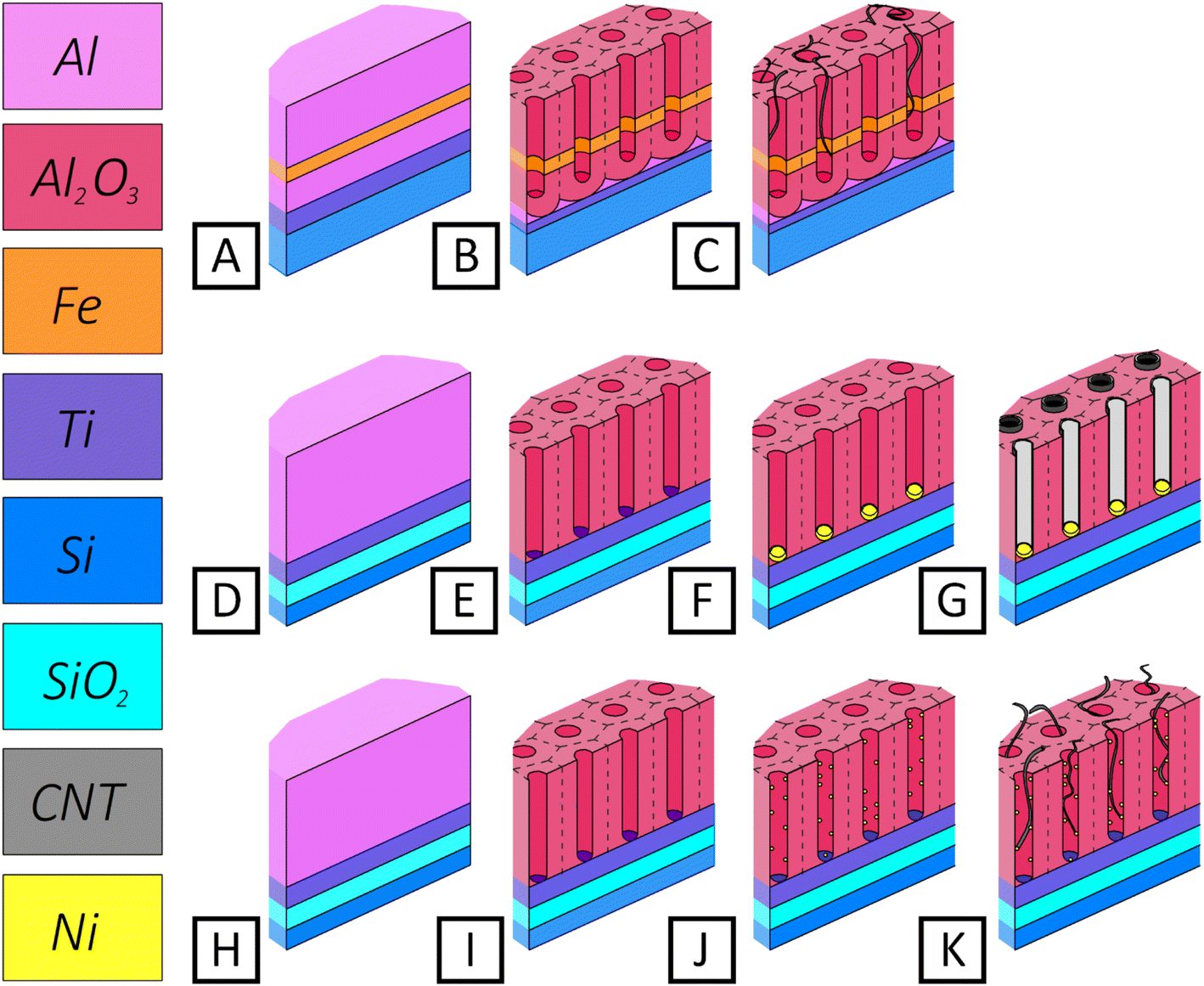 | ||
| Fig. 1 Simplified schematic representation of CNT synthesis stages: the variant from ref. 42 (A–C), (A) initial structure of thin film; (B) structure after through anodization; (C) structure after CNT synthesis; our proposed variant 1 (D–G), our proposed variant 2 (H–K): (D and H) initial thin film structure; (E and I) structure after through anodization of aluminum film (PAA); (F) structure after Ni deposition into the pores of PAA at constant potential (DC deposition), (J) structure after Ni deposition into the pores of PAA at alternating current (AC deposition); (G and K) after CNT synthesis. | ||
Fig. 1 shows three variants of fabricating vertically oriented CNTs in thin film PAA—according to the work of Maschmann and Franklin42–44 (A–C), and those proposed in this work, variants 1 (D–G) and 2 (H–K). On relatively coarse-grained aluminum films (deposited by electron beam evaporation), the creation of a continuous Fe thin film is likewise uncertain. The authors of this concept assert that for optimum structures (Fe film thickness in the order of 0.5 nm to 2.0 nm), a higher filling percentage (Maschmann variant) can be obtained.
This work compares the properties and processes for fabricating arrays of ordered, vertically oriented MWCNTs on Ni catalyst nanoparticles (NPs) of different sizes integrated in a thin-film PAA template's pores. On an oxidized Si substrate, a Ti electrode layer and an Al base layer are the basic components of the structure. A thin porous alumina with an ordered pore structure is produced from the Al film. Ni is electrochemically deposited into PAA pores to create catalyst nanoparticles with diameters of 10 ± 5 nm and 35 ± 5 nm in two separate electrochemical deposition regimes: variant 1 at constant potential (DC deposition) and variant 2 at alternating current (AC deposition).
CNTs were obtained using a metal catalyst electrodeposited on the bottom of the PAA pores – variant 1,45 or the nanotubes can be catalyzed on the pore walls – variant 2.46,47 Arrays of vertically oriented MWCNTs were formed by high-temperature chemical vapor deposition (CVD) using thin PAA as a template. The electrode system needs to be sufficiently heat-resistant because the fabrication of MWCNT arrays is carried out at a temperature of 1173 K. Thus, thin Ti films were used for the bottom electrode. Thus, Ti/PAA/Ni/CNT-based nanocomposite multilayered structure was formed on Si-substrate. The application of the obtained nanocomposite material based on arrays of ordered, vertically oriented MWCNTs on Ni catalyst nanoparticles is associated with their inherent properties of adsorption and control of reactions in adsorbed layers. The combination of these properties determines their surface functionality, a manifestation of which, in particular, is sensor sensitivity. Nowadays, improvements in the field of composite nanomaterials, filtration membranes, catalysts, sensors, CNT electrodes for biomedical applications, and so forth include not only their technological integration but also an evaluation of these materials' practical performance. Examining the functional characteristics of nanocomposite materials' surfaces in relation to external factors seems like a very promising task.
Therefore, the focus of this work is to: develop the method of using thin porous anodic alumina on a solid substrate to form arrays of vertically oriented carbon nanotubes localized on metal electrodes; conduct an extensive examination of the morphological, structural, and electrochemical (functional) properties of the surface of the resulting nanocomposite material. The work presented herein not only reports the fabrication of ordered arrays of CNTs on Ni NPs of different diameters by varying the electrodeposition conditions and using PAA templates, but also proposes the growth mechanisms of two types of carbon nanotubes, respectively.
2 Experimental
2.1. Sample preparation
The aluminum layer's porous anodization was carried out by a two-step method48 using a potentiostatic technique in a 4% H2C2O4 aqueous solution at a voltage of 40 V and an electrolyte temperature of 287 K. This method was first proposed by Nilsch et al.,48 but we slightly modified this method so that when the Ti film was reached, it was not anodized.
The first stage of anodizing is carried out at a voltage of 40 V for 10–15 min (depending on the Al film thickness), after which the oxide is removed by selective chemical etching; the second stage of anodizing of the remaining Al film is carried out at a voltage of 40 V until the current begins to drop for 15–20 min and then the voltage is reduced to 35 V and the process continues for 40 min until the current drops completely. At this voltage, the barrier layer was electrochemically dissolved for 40 minutes, using the procedures outlined in ref. 49 and 50. At this time, gradual electrochemical dissolution of the barrier layer occurs, mainly at the bottom of the oxide pores and Al anodization residues between the oxide cells. During the process of barrier layer thinning, not only its thickness decreases but also the morphology of the surface of the barrier layer changes, and the internal interface between the oxide and the Ti film becomes almost planar. The Ti film is not anodized through the porous oxide. The columns of TiO2, as described in ref. 51 and 52, are not formed (Fig. 2). The thickness of the matrix depends on the thickness of the Al film and is (0.6–1.5) ± 0.01 μm, the diameter of the pores is (45 ± 5) nm, and the pitch of the matrix is (110 ± 5) nm.
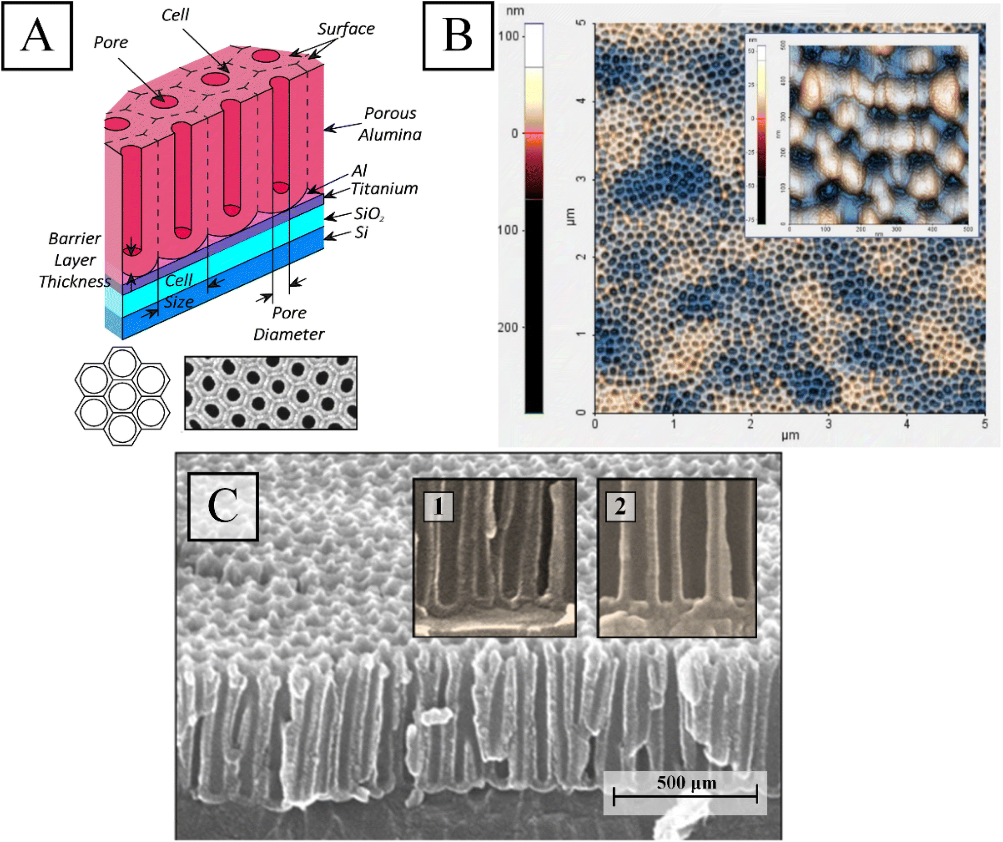 | ||
| Fig. 2 Schematic (A), 2D AFM after the pores widening (B), and SEM (C) images of PAA on Ti film prior to Ni deposition; insets of (A) show schematic and SEM images of PAA cells (top view); insets of (C) perform fragments of PAA cross-section before (1) and after (2) thinning of the barrier layer at the bottom of the PAA pores. | ||
Fig. 2 depicts a conceptual PAA (A) image, a 2D AFM image of the surface of the examination sample after barrier layer thinning (B), and a SEM image of the PAA cross-section (C) prior to Ni deposition in the PAA pores. Schematic and SEM images of a fragment of the sample surface are shown in the insets. In the inserts in Fig. 2C are shown fragments of PAA sample cross-section before and after thinning of the barrier layer at the bottom of the PAA pores.
Two sample variations were created: in the first variant (sample no. 1), the Ni catalyst was deposited at constant potential (DC deposition) following the weakening of the barrier layer; in samples of the second variant (sample no. 2), additionally, the pores were widened by chemical etching, and then Ni was electrodeposited at alternating current (AC deposition). The need to expand pores by chemical etching will be explained below when describing the process of CNT deposition.
In the course of the experiment, two variants of samples were fabricated that differed in the way the barrier layer was etched and the Ni catalyst was deposited: at constant potential (DC deposition for variant 1 (sample no. 1)) and at alternating current (AC deposition for variant 2 (sample no. 2)). The barrier layer was taken off (thinned) for two different sample types. SEM images of the PAA's surface and cross-section created using the two-step anodizing Al film process are presented in Fig. 3.
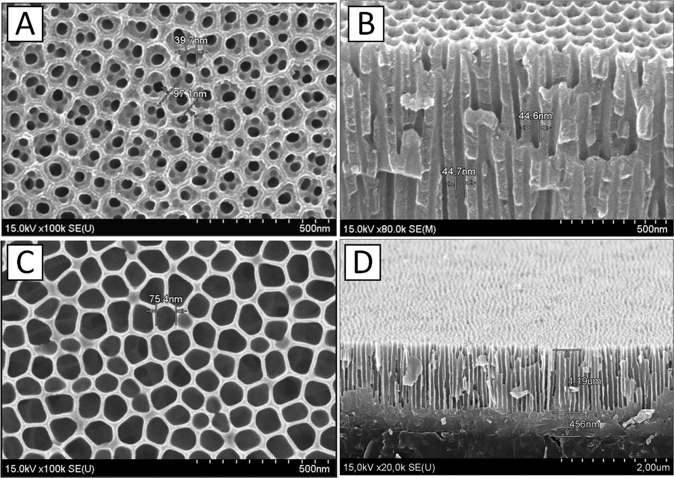 | ||
| Fig. 3 Surface and cross-sectional SEM images of PAA obtained in the two-step mode of anodizing aluminum film for two variants of samples: (A and B) sample no. 1, after thinning the barrier layer, (C and D) sample no. 2, after barrier layer thinning and pores widening. | ||
The image (Fig. 3A) shows PAA pore sizes after barrier layer thinning, sample no. 1. SEM image (Fig. 3C) shows PAA pore sizes after barrier layer removal and film thicknesses (Fig. 3D) for sample no. 2. For sample no. 1, the Ti layer thickness is about the same, and the PAA thickness can be larger (up to 3 μm).
For the first variation samples, the barrier layer that remained at the bottom of the PAA pores was removed immediately prior to Ni deposition by cathodic dissolution in the Ni deposition electrolyte at −3.0 V for three minutes, as described in ref. 45–54.
As a result, the obtained matrix with through channels had the following parameters: pore diameter (50 ± 5) nm, matrix pitch (110 ± 5) nm (sample no. 1) (Fig. 3A). This method of etching the barrier layer was chosen to minimize the increase in pore diameter, since the smaller the pore diameter, the smaller the catalyst particle size during the DC deposition. Below, it will be shown that the CNT formation mechanism in PAA and the obtained CNT properties depend on the catalyst particle size.
In the samples of variant 2, the barrier layer removal was performed by conventional selective chemical etching by immersing the sample in an aqueous solution containing 5% H3PO4 at a temperature of (35 ± 2) °C for a duration of 10 minutes, as represented in ref. 55, and the increase in the pore diameter was (75 ± 5) nm (sample no. 2 in Fig. 3B). It will also be shown that increasing the pore diameter is a prerequisite for forming CNTs in PAA on AC-deposited catalyst particles. It should be noted that the PAA films in both cases had identical initial parameters, since they were obtained in the same mode in a single technological cycle. The need for different etching processes of the barrier layer was experimentally established while working out the deposition process of CNTs in PAA with different dimensional parameters. Table 1 shows the parameters of the PAA experimental samples after removing the barrier layer at the bottom of the pores.
| Sample type | Anodizing voltage U, V | Pore diameter d, nm | Cell diameter, D, nm | PAA thickness, H, μm | Porosity α, % | Barrier layer thickness, B, nm | Wall thickness, W, nm |
|---|---|---|---|---|---|---|---|
| No. 1 | 40 ± 0.5 | 50 ± 5 | 110 ± 5 | 3.0 ± 0.05 | 20 | 33.6 | 30.0 |
| No. 2 | 40 ± 0.5 | 75 ± 5 | 110 ± 5 | 1.27 ± 0.05 | 45 | 19.6 | 17.5 |
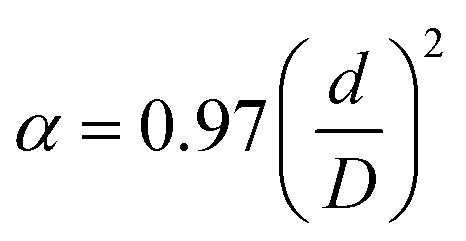
Such an important PAA parameter as porosity α depends on pore diameter and channel structure and was determined by the formula from:56
 | (1) |
The thickness of the cell walls (W) and the barrier layer (B) are two additional crucial PAA microstructure parameters that are displayed in Table 1. The following formula can be used to calculate the cell wall thickness W for perfectly arranged, densely packed hexagonal cells of the PAA membranes with a diameter d:56
 | (2) |
Besides, the thickness of walls is related to the barrier layer's thickness as the following ratio:57
| B = 1.12W | (3) |
In the electrolyte NiSO4·7H2O (140 g l−1) + NiCl2·6H2O (30 g l−1) + H3BO3 (25 g l−1) + Na2SO4 (60 g l−1), the catalyst Ni NPs were created by electrochemical deposition.58 The electrolyte's temperature was 293 K, with a p-value of 5.2. HANNA Instruments' HI83141 pH meter was used to measure the electrolyte's pH. To correct the pH, sodium hydroxide (NaOH) was added.
In the first case, catalyst particles of (35 ± 5) nm were obtained by DC deposition at −1.6 V for (1–3) min.45 Ni catalyst nanoparticles of (10 ± 5) nm size were produced by alternating current deposition (AC deposition) with the following parameters: frequency is 180 Hz; voltage is 3 V; current density is 10 mA cm−2; duration is 3 min. Information can be found in our recent article.46
Electrochemical deposition and anodizing parameters were managed using a P-5827 potentiostat (sample no. 1) and a specially designed laboratory setup based on a GZ-123 low-frequency signal generator (sample no. 2), respectively.
CNTs were created from hydrocarbons by high-temperature pyrolysis of a liquid hydrocarbon, decane C10H22, using chemical vapor deposition. The Ni NP-containing experimental samples in the PAA were put in a tubular quartz reactor called “Nanofab-1” that was particularly made for the purpose. The procedure was conducted at atmospheric pressure using Ar/NH3 as the carrier gas. The addition of ammonia enhanced the catalytic activity of the Ni nanoparticles. The argon flow rate was 100 cm3 min−1, the NH3 flow rate was 10 cm3 min−1, and the reaction zone temperature was 1173 K. The duration of the synthesis varied between 30 and 90 seconds. The cooling rate was set by the heater's natural cooling process.
2.2. Sample characterization
Scanning electron microscopy (SEM; Philips XL 30 S FEG, FEI Company, USA); transmission electron microscopy (TEM; Philips CM-30, FEI Company, USA); atomic force microscopy (AFM; Nanotop NT-206, “Microtestmachines,” Belarus); and Raman spectroscopy (3D scanning laser confocal Raman microscope-spectrometer – Nicolet “NEXUS Confotec MR350” (SOL Instr., Belarus)) were used to examine the samples' surface topography and microstructure in both top and cross-sectional views. CNTs were separated from the template by sonicating them in isopropyl alcohol for 20 minutes and then centrifuging them for 10 minutes to provide samples for TEM examination. Using a modified DRON-3M diffractometer (NPO Burevestnik, Russian Federation) with CuKα radiation (λ = 0.154242 nm), X-ray diffraction analysis (XRD) was used to examine the crystal structure of Ni nanoparticles.The Ti/PAA/Ni/CNT-based nanocomposite material was subjected to electrochemical tests utilizing an AUTOLAB/PGSTAT302N potentiostat/galvanostat (Netherlands, Utrecht). 1.10 version of the NOVA program was utilized to process the data. The standard silver–silver chloride reference electrode, EVL-1-M3.1 (Ag/AgCl/KCl), and an auxiliary platinum electrode were used in a three-electrode cell for the tests. An artificial physiological solution containing 0.9% NaCl was used for all tests.51 Applying a pH-HI 83141 pH meter from HANNA instruments, the electrolyte's pH was 6.34 ± 0.02 when measured. Every reagent employed to prepare the solutions was of a grade that was chemically pure. Distilled water was used to prepare the solutions.
Artificial physiological solutions imitate the liquids that are employed as a foundation for the processing of analyte samples in microbiological analyses (here, background electrolytes). Every measurement was done with natural aeration (no stirring) and at room temperature. The examined samples had a surface area of 0.6 × 0.6 cm2 (0.36 cm2). To eliminate the diffusion potential between the electrolyte and the reference electrode electrolyte, a silver chloride reference electrode with the same electrolyte composition was used. Details added to Section 3.2 of the article.
3 Results and discussion
3.1. Synthesis method
 | ||
| Fig. 4 SEM images of the surface of experimental samples after Ni deposition: (A) sample no. 1 (DC deposition), the inset shows the scheme of formation of complex shape of Ni NPs in sample no. 1 (DC deposition) and (B) sample no. 2 (AC deposition), the inset shows a fragment of the cross-section of this sample; (C and D) AFM high-resolution images of the cross-sectional distribution of filled and empty pores in sample no. 1. | ||
In the samples of variant 2, no dissolution of PAA was performed.
From the results shown in Fig. 4A, C and D, it can be seen that Ni NPs deposited at constant potential have a complex shape in the form of shallow cups with a small hill in the center. It also appears that the outer part of the nanoparticles has an almost cylindrical profile (repeating the shape of the oxide pores), while the inner part of the NPs has a conical profile.
Several papers have proposed different mechanisms of pore filling and formation of either nanowires or nanotubes during the electrochemical deposition of metals.63–66 In some works, it is believed that the shape of the pulse signal (in pulsed deposition) determines the morphology of the produced structure. In other works, it is assumed that the result depends on the value of the voltage in the pulse. The consensus is that the formation of hydrogen bubbles is responsible for the formation of the various structures. Their number and size determine the deposition mechanism and thus the shape of the precipitate: nanowires, nanotubes, or a more complex pattern. In all proposed variants, it is noted that for DC deposition at a fixed potential, the deposition mechanism involves bottom-up growth (from the bottom of the pore to its surface) and in wide range of potential values, from equilibrium to −4 V. This is confirmed by the different height of the metal columns due to the different pore diameter of the thin film oxide (pore diameter variation in the order of 10–15%). That is, the deposition rate in the longitudinal direction (from bottom to top) is higher than in the radial direction, so that such a complex shape of sediment is formed in such a short period of growth.
Therefore, hydrogen release, which affects the shape of the nanostructures (either nanowires or nanotubes) and is related to the shape and/or magnitude of the voltage pulse, may be the cause of the variable Ni deposition rates in the two channel orientations (longitudinal and radial).67
It should be noted that the shape of the NPs obtained in this particular case (DC deposition was performed at −1.6 V for 3 min), Fig. 4A and C, during CVD synthesis favors the formation of exactly CNTs rather than nanowires or nanofibers. In the following, the presumed growth mechanism of such CNTs will be described in more detail.
From the images in Fig. 4B, it can be seen that the Ni deposition by AC deposition is discrete in the small nanoparticles (clusters) form with a 10 nm diameter along the entire length of the pores. As a result, compared to DC deposition, the deposition occurs along the pore walls from the bottom to the surface (bright spots in the inset of Fig. 4B). This is probably due to the treatment of the inner pore surface in a 4% aqueous H3PO4 solution in the process of pore diameter expansion (barrier layer thinning). It is believed that AC deposition occurs in the presence of the barrier layer at the pores bottom, i.e., there is no need for the preliminary operation of thinning the barrier layer. However, in this case, we found that since the pore is partially filled with the NP catalyst along the entire length, to enhance the conditions for the transit of hydrocarbon molecules during the CNT production process, the pore diameter must be expanded (by thinning the barrier layer).
Thus, the deposition mechanisms for DC and AC are different and are largely determined by the waveform (frequency), which in turn determines the type of motion and diameter of the hydrogen bubbles. At constant voltage, the diameter of the bubbles does not change, and hydrogen release occurs from bottom to top (the classical mechanism of electrochemical deposition in bottom-up channels). At AC voltage, the mechanism of deposit formation in the form of nanoparticles (nanoclusters) may be similar to the mechanism of NT formation proposed in ref. 63–67 for PAA and polycarbonate membranes. When high-frequency AC pulses are applied, the cathode current increases almost instantaneously at voltage transitions from 0 to −4 V, and larger hydrogen bubbles are formed that separate more easily from the channel bottom than from the side walls, thus shielding the channel sides. Ni can only be deposited in the gap created by the hydrogen bubbles and the pore wall in these circumstances. Individual nanoparticles develop as a result. When gas bubbles detach from the deposition surface and are discharged out of the pore, new Ni deposition can proceed on this surface prior to the appearance of new hydrogen bubbles. Ni is thus deposited at different rates in the area next to the pore wall and perpendicular to the wall because the time that hydrogen bubbles shield the surface at the bottom of the nanotubes is longer than the period that the surface is electrochemically active. The Ni deposition process can proceed as long as there are no gas bubbles on the surface after the hydrogen bubbles are expelled from the channels' pores and outside.
All other conditions being equal (frequency, voltage, current density), only single nanoclusters that are statistically distributed along the pore have time to form during the short-term deposition (3 min) (Fig. 4B). At longer polarization periods, the number of Ni clusters increases, the walls of the channels and the bottom of the pores are gradually filled with the metal deposit, and nanotubes are formed. Further increasing the deposition time leads to the formation of nanopillars (nanowires), so it is very important to choose the right deposition mode to obtain a certain shape of the precipitate.
We have empirically identified the domain where the distribution of the Ni clusters is roughly uniform along the whole length of the pore. The clusters' number is determined by the deposition period (we examined the range of 1–5 min), while their diameter is determined by the deposition frequency (we studied the range of 100–280 Hz) and voltage (we studied the range of 2–5 V). The optimal mode is: frequency is 180 Hz, voltage is 3 V, current density is 10 mA cm−2, duration is 3 min.
During CNT production, the catalyst nanoparticles' surrounding aluminum oxide is thought to keep them from aggregating and preserve their catalytic activity.39,68–71 The crystal structure of Ni NPs in Al2O3 was investigated using the X-ray diffraction method (Fig. 5). In both instances, the nickel phase is crystallized by the face-centered cubic (fcc) lattice with orientations (111), (200), and (220), with the Ni (111) phase predominating. The Debye–Scherer equation and XRD data processing were used to calculate the average size of Ni (111) crystallites. The crystallite diameters of the Ni NPs in version 1 samples vary from 18 to 20 nm, while those in variant 2 samples range from 13 to 15 nm.
 | ||
| Fig. 5 XRD results of Ni-NPs electrodeposited in PAA: (A) variant 1, sample no. 1 (for the sample shown in Fig. 4A), (B) variant 2, sample no. 2 (for the sample shown in Fig. 4B). | ||
In the first case (Fig. 5A), Ni is located only at the bottom of the PAA pores, in which the barrier layer was etched by conventional chemical etching (i.e., Ni on the Ti layer). Therefore, this spectrum contains a reflection from Ti. In the second case (Fig. 5B), the barrier layer in the PAA was not removed, and AC-electrodeposition was carried out in the oxide with a barrier layer to show the difference in the deposition processes at DC and AC regimes. Therefore, in the second case, there is no reflection from Ti, but there is a reflection from the PAA.
Thus, the proposed methods allow obtaining catalyst NPs of different sizes and localization in the PAA template. As a result, it will be shown below that this causes two different mechanisms of CNTs deposition with different morphological and structural properties (shape, size, quality of CNTs' walls).
 | ||
| Fig. 6 SEM images of sample no. 1 (A and B) obtained via DC deposition of Ni in the pores. Inset (A) shows a magnified image of the surface of PAA with Ni NPs at the bottom of the pores before MWCNT deposition, inset (B) shows a magnified image of a fragment of the sample with MWCNTs. (C) SEM image of the cross section of sample no. 2 after AC deposition of Ni NPs at the bottom of PAA pores; (D) SEM image of the surface of this sample after synthesis of MWCNTs in PAA pores; the insets (C and D) show enlarged fragments of these images. (E) SEM images of the surface and cross section (F) of sample no. 2 and enlarged fragment of image (F). | ||
After CNT synthesis, ion cleaning of the sample surface was performed by bombardment with 3 keV argon ions in the “Oratoria-9” machine. In ion etching, the matrix material (anodic aluminum oxide) sputters faster than the tube material, causing the tubes to protrude above the surface of the PAA matrix.
Extensive research has demonstrated that, only on Ti contact electrodes, a carbon nanocomposite material is created from a variety of carbon nanotubes locally implanted in porous alumina. The tubes are smooth-walled cylinders that are aligned perpendicular to the substrate. Their outside diameter is equal to the PAA pore diameter, and their height is either the same as or slightly more than the PAA thickness. By altering the PAA height, the CNT length can be precisely regulated within the range of (0.5–2.5) μm with an accuracy of ±20 nm. The conditions of deposition affect the tubes' inner diameter. The inner diameter of the tubes shrinks as the deposition time increases, and the tubes may eventually turn into carbon nanofibers. The quality (regularity) of the PAA determines the degree of pore filling, which ranges from 70 to 80%. The density is 1.1 × 10⁹ CNT per cm2 on average.
Carbon reduction from the hydrocarbon carrier (decane) on Ni NPs and its conversion into a solid crystalline phase result in the nucleation of graphite islands at the bottom of pores. This mechanism fundamentally determines the form of the crystalline carbon phase by saturating and supersaturating the catalyst particle with carbon. The rough pore surface facilitates effective fixation of carbon atoms. Single-atom graphite (graphene) flakes are used to create tubes with walls. These tubes are known as multilayer carbon nanotubes with a papier-mâché-like structure in the literature.72
The CVD synthesis results of MWCNTs in PAA pores according to variant 2, using Ni NPs obtained by AC deposition (sample no. 2), are shown in Fig. 6C–F. Fig. 6C shows the SEM image of sample no. 2 after AC deposition of Ni NPs at the bottom of PAA pores before CNT deposition. As demonstrated in Fig. 6D, only one CNT with a (10–20) nm diameter develops in each pore. Fig. 6E and F shows SEM images of the surface (E) and cross section (F) of sample no. 2, explaining the nucleation mechanism of MWCNTs in this case. Tube nucleation takes place in clusters that are located in pores at different depths (Fig. 6F). Therefore, the tube lengths vary. The longest tubes are formed in clusters located almost on the pore surface, so they are longer and gather in bundles. In this mode of CNT deposition, the pore surface is open and not blocked by carbon black precipitates. The vertical orientation of the CNTs and small CNT bundles is maintained or seems to be looped vertically.
Despite the presence of numerous almost identical Ni NPs in each pore, the findings demonstrate that only about 70% of the pores produce CNTs, and only one CNT can be seen in each catalytically active pore. This could be a result of the Ni particle size characteristics, the limited supply of gaseous carbon deep inside the pore, and the relatively high activation energy needed for CNT nucleation. In some works,73–75 it is pointed out that each pore can be considered a chemical microreactor in which multi-atomic molecules are in motion. This approach assumes a preferential concentration of reactants and catalysts in a limited volume, with the reactants isolated from the surrounding environment. After nucleation, the nanotube continues to grow vertically up to the PAA surface, where the unrestricted delivery of the carbon mixture is available. It is important to note that most nanotubes are formed on Ni NPs that are deep inside the pore and not on the surface.
Note that in the process of sample cleavage, CNTs are partially separated from their nucleation sites in pores. Therefore, it is difficult to identify CNT nucleation sites within the pore by cross-sectioning. The formation of CNT bundles also makes it difficult to determine the location of the nucleus of individual CNTs in the pore. Therefore, SEM images of the surface (Fig. 6D) were used to determine the density of CNTs growing out of PAA pores. It is estimated that for a given film structure, approximately 50–70% of the pores generate CNTs (depending on the thickness of the PAA), and only one CNT appears in each catalytically active pore. The maximum yield percentage was observed for samples with a PAA thickness of (0.8–1.1) μm.
Table 2 displays the parameters of the carbon nanotube array embedded in the PAA for the two sample variations.
For comparison, the specific density of the CNTs in the PAA template in ref. 42 is 10%. The specific density of CNTs (up to 90% pore filling) is anticipated to rise with further modification of the Al film anodization procedure (pore diameter and regularity), Ni AC deposition parameters (crystallite size), and CNT synthesis conditions (temperature and duration). Although the majority of the CNTs visible on the PAA surface are vertically oriented, it is anticipated that when a negative potential is applied to the base during CVD synthesis, the degree of CNT alignment will improve.76 Some work has shown that self-organized, unidirectional (vertical) CNTs exhibit faster heterogeneous electron transfer than randomly scattered ones.77 The reason for this lies in the fundamentals of the electrochemistry of CNTs. The modified CNTs on gold electrodes, both with randomly dispersed and self-organized CNTs, showed that the electron transfer dynamics strongly depends on the orientation of the nanotube. The electron transfer rate in disordered CNTs is 40 times lower than that in self-assembled CNTs.
TEM images of individual MWCNTs for the two sample variants are shown in Fig. 7: (A) sample no. 1, (B) sample no. 2. The comparison of the images and the data in Table 1 demonstrates that the tubes are significantly different. In the first case, the nanocomposite material has a more ordered structure, but the dimensional parameters of the tubes do not correspond to the classical concept of CNTs, in particular MWCNTs.
 | ||
| Fig. 7 TEM images of two variants of MWCNTs: (A) sample no. 1, (B) sample no. 2. The insets show the HR-TEM images of the CNTs. The red arrow indicates a catalyst particle (Ni) in the form of a sphere (bead). (C and D) shows fragments of MWCNTs of the two variants. | ||
In contrast to multilayer CNTs with a “Matryoshka doll” or “roll” type structure, which are MWCNTs of a new type, the CNTs of the first variant have an ordered wall structure of statistically oriented graphite plates spaced about 0.34 nm apart. Such plates are assembled into polycrystalline aggregates on the pore walls, forming vertically oriented layers (papier-mâché-type structures).72 The following is demonstrated by high-resolution TEM images (Fig. 7B).
The multi-walled CNTs of the variant 2 sample have a well graphitized structure with a graphene layer spacing of 0.34 nm, as in the classical MWCNTs.
Raman spectroscopy was used for further investigation of the nanotube structure. The Raman spectra of the two variations of MWCNTs synthesized in the PAA are shown in Fig. 8.
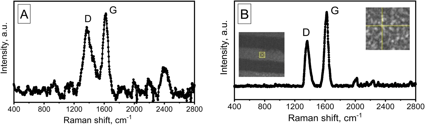 | ||
| Fig. 8 Raman spectra (λ = 473 nm) of MWCNTs for samples of two variants: (A) sample no. 1, (B) sample no. 2, measured at the location indicated in the photo, the inset shows surface SEM image of the experimental sample. | ||
The spectra have been found to contain two bands in the region of 1361 cm−1 (D band) and 1618 cm−1 (G band), respectively, which correspond to vibrational states of defects in the structure of the hexagonal carbon lattice, including the edges of carbon crystallites. The G band corresponds to the doubly degenerate phonon mode of the sp2 carbon network. The ratio of IG/ID intensities, which is the main indicator of CNT quality, is equal to 1.2 in variant 1 and nearly 1.6 in variant 2, suggesting that variation 2 of CNTs has a relatively high level of quality. It should be noted that the increased intensity of the D band may be related to the abundance of short nanotubes, where edge effects are more noticeable. Typical for MWCNTs, sample no. 2's Raman spectra (λ = 473 nm) includes D and G areas at about 1361 and 1618 cm−1, respectively.78
The Raman spectrum of sample no. 1 also shows a distinct band at 2450 cm−1. A comparison of these spectra (A and B) shows that this peak is most likely due to the influence of the substrate (PAA), as these tubes are formed on the PAA pore walls. In addition, it is likely that the growth mechanism of tubes of variant 1 differs significantly from the growth mechanism of tubes of variant 2 (classical growth mechanism on small-sized catalyst particles).
Several variants of the growth mechanism of classical CNTs are proposed. The widely acknowledged process for the formation of SWCNTs is the breakdown of the carbon source to elemental carbon on the catalyst particle's surface, which is then stored there and released when the concentration reaches a critical point to create CNTs.79–82 The function of the catalyst in the process of catalytic CVD is to form more reactive intermediates with pyrolysis products of carbon-containing compounds to reduce the activation energy of the chemical reaction of CNT formation. Catalysts (transition metals), have a number of important properties that affect the process of CNT synthesis, such as melting point, equilibrium vapor pressure, ability to dissolve carbon and form a chemical bond with it, etc. Carbon solubility is considered to be one of the most important properties of the catalyst in the CNT growth process.80,83–85 This is the mechanism by which variant 2 of CNTs is formed.
The proposed mechanisms of MWCNT growth on catalyst particles of 1–10 nm (ref. 57) make it difficult to explain the nanotube growth on catalyst particles of larger size (in sample no. 1, the size of catalyst particles is (30 ± 5) nm). Presumably, the conditions for the synthesis of CNTs in this specific instance (in porous PAA) are comparable to those for synthesis in a one-dimensional nanoreactor (in each alumina pore), and the oxide itself takes part in this process.86,87 In addition, crystalline alumina is frequently employed as a matrix in the epitaxial growth of lattice-mismatched semiconductors, and that anodic alumina crystallization processes start at the CNT synthesis temperature (1172 K) (while maintaining morphological parameters),88,89 there is a significant possibility that the synthesis of graphite flakes on PAA walls takes place by deposition or epitaxy processes.87
Decane (C10H22) molecules on the inner pore surface of alumina heated to 1172 K thermally decompose to create MWCNTs at the sites with Ni clusters at the bottom of the pores. At this temperature, hydrogen is desorbed, hydrocarbon molecules disintegrate into atoms, and carbon atoms move along the pore surface to form expanding graphite islands that eventually cover the pore's interior. In other words, synthesis, as thin film deposition, can be accomplished by thermally decomposing the gas on a relief substrate.
3.2. Electrochemical studies of the obtained Ti/PAA/Ni/CNT-based nanocomposite material
Applying a linear anodic polarization measuring technique, the electrochemical processes on the surface of the Ti/PAA/Ni/CNT-based nanocomposite material were investigated. Linear sweep voltammograms were utilized to measure the currents and corrosion potentials. A series of experiments were carried out to investigate the electrochemical properties of nanocomposite interfaces. This method is widely used to study the kinetics of electrode processes, in which the potential of the electrode changes over time (usually according to a linear law) and the current flowing through the electrochemical cell is measured.58 It is based on obtaining and analyzing the current–voltage dependences of the interface between a polarizing electrode and an electrolyte solution. Using linear sweep voltammograms, one can approximately test the reversibility of the electrode system, determine whether multisteps occur, and recognize faradaic and non-faradaic adsorption–desorption processes.90,91The Ti/PAA/Ni/CNT-based nanocomposite material was subjected to electrochemical tests utilizing an AUTOLAB/PGSTAT302N potentiostat/galvanostat (Netherlands, Utrecht). 1.10 version of the NOVA program was utilized to process the data. An artificial physiological solution containing 0.9% NaCl (pH: 7.0 to 7.5) was used for all tests. Artificial physiological solutions imitate the liquids that are employed as a foundation for the processing of analyte samples in microbiological analyses. In accordance with “Microbiology of Food and Animal Feed. General requirements and guidance for microbiological examinations” (ISO 7218-96),92 the tests were conducted.
Preliminary studies58 have shown that PAA is passive in the wide potentials range from −1.0 to +1.0 V (Ag/AgCl) and makes an insignificant contribution to the corrosion current of the nanocomposite. Evaluation using previous SEM investigations (Fig. 4 and 5 presented in our previous work58) and polarization measurements showed that there were no signs of surface degradation of the Ti electrodes. Alumina on the working surface of the electrode does not prevent the deposition of Ni into the pores since a fairly good contact is formed with the Ti film. Titanium in the electrode area (without alumina) also shows high chemical resistance under these experimental conditions.
Next, we studied the behavior of the Ni catalyst deposited into the PAA pores using DC- and AC-electrodeposition. The results of the linear sweep voltammetry are shown in Fig. 9A–D for two variants of samples: in sample no. 1, Ni was deposited in PAA using DC-electrodeposition, and in sample no. 2, Ni was deposited in the same electrolyte but with AC-electrodeposition. Fig. 9A–D shows linear sweep voltammograms depending on the immersion time of the samples in the background electrolyte (0.9% aqueous NaCl solution). For Ti/PAA/Ni samples obtained via DC-electrodeposition (sample no. 1): (A) dependence 1 – after 5 min after immersion, (B) dependence 2 – after 45 min; for Ti/PAA/Ni samples obtained via AC-electrodeposition (sample no. 2): (C) dependence 3 – after 5 min; (D) dependence 4 – after 45 min.
 | ||
| Fig. 9 Linear sweep voltammograms for Ti/PAA/DC-Ni (A and B), and Ti/PAA/AC-Ni (C and D), linear sweep voltammograms of samples after MWCNTs deposition into the PAA pores: (E) sample no. 1, (F) sample no. 2. Background electrolyte: 0.9% aqueous NaCl solution. | ||
From the presented results, it is evident that after holding sample no. 1 in the background electrolyte for 45 min, the current density (anode branch) decreases and stabilizes at a lower level (dependence 2, Fig. 9B) compared to the moment of immersion (dependence 1, Fig. 9A). The open-circuit potential increases slightly to −0.263 V as Ni passivation occurs on the surface of nanoislands. For the samples of the second variant (sample no. 2), such a tendency is not observed. It is seen from Fig. 9D that after holding the sample in the electrolyte for 45 min, the open-circuit potential changes from −0.163 V for Ni (dependence 3) to −0.458 V for Ti (dependence 4), i.e., it can be assumed that AC-Ni has almost completely dissolved during this time. The current density increases sharply without any limitation in magnitude. But this may be due to the size and discrete nature of the Ni nanoparticles, which are distributed along the pore walls to the surface. In this case, the area of the treated surface is significantly larger, and the current density increases (S2 ≫ S1), as presented in the insert of Fig. 9D. In general, samples of the second variant with AC-electrodeposited Ni showed the possibility of operation in this background electrolyte for a time not exceeding the 25–30 min (in linear sweep voltammograms of AC-Ni, there is no current stabilization section). Samples with DC-Ni show greater stability up to 45–50 min.
Next, electrochemical studies of the Ti/PAA/Ni/MWCNT samples were carried out. Fig. 9E and F show the linear sweep voltammograms of the samples after CNTs deposition in the PAA pores of the first (E) and second variant (F) after 15 min of immersion in the background electrolyte. In the first case, the inner surface of the PAA pores is actually covered with a continuous layer of carbon material after the MWCNTs deposition of the first type of (sample no. 1) on the DC-Ni catalyst. In the second case, the voltammograms for samples of the second variant with deposited MWCNTs also show the stability of the polarization current after 15 min of immersion in the background electrolyte. The nature of the obtained dependencies (rapid stabilization of current) shows that such structures can operate in this background electrolyte for a longer time (up to 40 min).
The obtained results show that both variants of forming the composite material arrays of MWCNTs on Ni NPs are suitable for use in biosensing applications. In this case, the electrochemical properties of the composite material and the dimensional parameters of the bioobjects are of greater importance. We employed C2H2O4 (oxalic acid) in our work, but other electrolytes can also be used to create PAA templates, allowing for pore sizes between 20 and 200 nm and pore densities ranging from 109 to 1011. Since in the first variant the diameter of MWCNTs corresponds to the diameter of pores, this possibility can be used (to change the diameter of pores and MWCNTs). In the second variant, as preliminary studies have shown, the use of the H2SO4 (sulfuric acid) electrolyte for the formation of PAA allows to obtain not CNTs, but carbon fibers, which completely fill the pores and have the diameter equal to the diameter of pores. Such fibers can also be used, but this will another story (another work). We used the electrolyte that allows to compare the results when obtaining MWCNTs of different types.
The quality of MWCNTs in the second variant is higher and corresponds to the quality of conventional MWCNTs obtained by the CVD method, so they can be used in the manufacture of other CNTs-based electronic devices that require a close pack ordering. When used for biosensing applications, the electrochemical properties of the nanocomposite material and the dimensional parameters of bioobjects are more important. These parameters include sizes corresponding to the sizes of a number of viruses (from 2 to 400 nm), proteins (from 5 to 50 nm) and geometric parameters of genes (width 2 nm and length from 10 to 100 nm),93 ensuring good dimensional compatibility and possibilities of their practical use. It is possible to change the pore sizes and distances between them in a fairly wide range, using various electrolytes and technological regimes during anodization process (Table 3).56,57
| Electrolyte | Anodizing voltage (V) | Interpore distance (nm) | Pore density (per cm2) |
|---|---|---|---|
| (1) H2SO4 (sulfuric acid) | 25 | 63 | ∼1011 |
| (2) C2H2O4 (oxalic acid) | 40 | 105 | ∼1010 |
| (3) H3PO4 (phosphoric acid) | 195 | 500 | ∼109 |
Thus, both variants of forming the nanocomposite material arrays of MWCNTs on Ni NPs are suitable for use in biosensing applications.94–96 But MWCNTs obtained by the second variant can also be used in other applications for electronic devices that require a close pack ordering.97
4 Conclusion
Ti/PAA/Ni/CNT-based nanocomposite experimental samples were fabricated. Two variants of template synthesis of MWCNTs in PAA pores are considered, which differ in the way of etching the barrier layer and the mode of Ni catalyst deposition: at constant potential (DC deposition) and at alternating current (AC deposition). Using CVD and common microelectronics technological processes, such as vacuum deposition of thin metal films, photolithography, and electrochemical deposition, MWCNTs can be integrated into planar electrodes of biosensors of a sufficiently large size in the experimental structures under investigation in both variants.This work not only reports the fabrication of ordered arrays of MWCNTs on Ni NPs of different diameters (varying the electrodeposition conditions) using PAA templates but also proposes growth mechanisms for two types of MWCNTs. The formation of different types of MWCNTs in identical PAA templates is explained by the fact that different methods of electrochemical deposition of Ni NPs, which are used as catalysts in the synthesis of CNTs, form different types of Ni NPs in the pores of PAA, which in turn change the growth mechanism of CNTs. Both variants for formation of the nanocomposite material arrays of MWCNTs on Ni NPs are suitable for use in biosensing applications.
According to electrochemical research, the morphological characteristics (porosity, surface development) that are dictated by the catalyst and the conditions for obtaining oxide layers have a major effect on the charge transfer process at the interface between the metal-oxide heterostructure and the corrosion-active environment. This, in turn, determines the electrochemical properties of the Ti/PAA/Ni/CNTs nanocomposite material, including its anti-corrosion capabilities. In particular, it was revealed that the intensity and stages of corrosion are mainly determined by the chemical stability of the catalyst nanoparticles included in the nanocomposite material.
Further work is being continued to increase the specific density of CNTs, their quality and degree of alignment (CNTs of the second type) by improving the process of anodization of Al film (diameter and regularity of pores), electrochemical deposition parameters of Ni (crystallite size), and conditions of CNT synthesis (temperature and duration), as well as the optimization of the reactor design for CNT synthesis.
Aside from enabling the quick identification of bacterial or viral infections, the results obtained could be practically helpful for future advancements in the field of electrochemical detection of biological objects, specifically for the detection of small biologically active molecules, high molecular-weight compounds, and natural nucleic acid targets.98–100 The results show that the employment of non-lithographically self-organized alumina templates with carbon nanotubes is a suitable method for creating nanobiosensors that can be integrated into existing semiconductor technology. Investigating this nanocomposite material's electrochemical characteristics will advance production techniques and forecast the long-term stability of structures built with it, such as sensitive components of biosensors and other nanodiagnostic devices.
Data availability
The data presented in this article are available from the corresponding author upon reasonable request.Author contribution
Daria I. Tishkevich, Alla I. Vorobjova formulated of overarching research goals and aims; Alla I. Vorobjova, Daria I. Tishkevich, Elena A. Outkina, Ihar U. Razanau, Tatiana I. Zubar, M. I. Sayyed, M. V. Silibin and A. Yu. Gerasimenko made investigations; Anastasia A. Rotkovich and Anastasia A. Bondaruk visualized the main results of the paper; Sergei V. Trukhanov prepared the graphics; Alla I. Vorobjova, M. V. Silibin and Alex V. Trukhanov supervised the project. All authors reviewed the manuscript.Conflicts of interest
The authors declare no competing interests.Acknowledgements
The work was carried out as part of a major scientific project with financial support from the Russian Federation represented by the Ministry of Science and Higher Education of the Russian Federation under agreement No. 075-15-2024-555 dated April 25, 2024.References
- G. R. Dangel, H. Kumakli, C. E. Rahm, R. White and N. T. Alvarez, Appl. Sci., 2021, 11(18), 8399 CrossRef CAS.
- M. Mabrouk, R. Rajendran, I. E. Soliman, M. M. Ashour, H. H. Beherei, K. M. Tohamy, S. T. N. Kalarikkal, G. Arthanareeswaran and D. B. Das, Pharmaceutics, 2019, 11(6), 294 CrossRef CAS PubMed.
- D. W. M. Arrigan, Analyst, 2004, 129, 1157–1165 RSC.
- N. Karimian, L. M. Moretto and P. Ugo, Sensors, 2017, 17(1), 65 CrossRef PubMed.
- Y. Tu, Y. Lin and Z. F. Ren, Nano Lett., 2003, 3(1), 107–109 CrossRef CAS.
- G. Liu, Y. Lin, Y. Tu and Z. Ren, Analyst, 2005, 130, 1098–1101 RSC.
- Y. Lin, F. Lu, Y. Tu and Z. Ren, Nano Lett., 2004, 4(2), 191–195 CrossRef CAS.
- Y. Liu, J. Zhang, Y. Cheng and S. P. Jiang, ACS Omega, 2018, 3(1), 667–676 CrossRef CAS PubMed.
- V. P. Menon and C. R. Martin, Anal. Chem., 1995, 67(13), 19201928 CrossRef.
- D. S. Kim, E. S. Kang, S. Baek, S. S. Choo, Y. H. Chung, D. Lee, J. Min and T. H. Kim, Sci. Rep., 2018, 8, 14049 CrossRef PubMed.
- M. A. Beluomin, N. Karimian, N. R. Stradiotto and P. Ugo, Sens. Actuators, B, 2019, 284, 250–257 CrossRef.
- R. Li, L. Cao, C. Liang, S. Sun, H. Liu and P. Yan, Ionics, 2020, 26, 4661–4670 CrossRef CAS.
- Z. Li, C. Liu, V. Sarpong and Z. Gu, Biosens. Bioelectron., 2019, 126, 632–639 CrossRef CAS PubMed.
- M. Ongaro, M. Signoretto, V. Trevisan, A. M. Stortini and P. Ugo, Chemosensors, 2015, 3(2), 146–156 CrossRef CAS.
- N. R. Shanmugam, S. Muthukumar, S. Chaudhry, J. Anguiano and S. Prasad, Biosens. Bioelectron., 2017, 89, 764–772 CrossRef PubMed.
- M. Jamal, M. Hasan, A. Mathewson and K. M. Razeeb, Biosens. Bioelectron., 2013, 40(1), 213–218 CrossRef CAS PubMed.
- A. Periyakaruppan, R. P. Gandhiraman, M. Meyyappan and J. E. Koehne, Anal. Chem., 2013, 85(8), 3858–3863 CrossRef CAS PubMed.
- J. Abbott, T. Ye, L. Qin, M. Jorgolli, R. S. Gertner, D. Ham and H. Park, Nat. Nanotechnol., 2017, 12, 460–466 CrossRef CAS PubMed.
- Z. Wang, R. M. Latonen, C. Kvarnström, A. Ivaska and L. Niu, Materials, 2010, 3(1), 672–681 CrossRef CAS.
- Y. H. Yun, Z. Dong, V. N. Shanov, A. Doepke, W. R. Heineman, H. B. Halsall, A. Bhattacharya, D. K. Y. Wong and M. J. Schulz, Sens. Actuators, B, 2008, 133, 208–212 CrossRef CAS.
- J. S. Ye, Y. C. Bai and W. D. Zhang, Microchim. Acta, 2009, 165, 361–366 CrossRef CAS.
- R. Lin, T. M. Lim and T. Tuan, Electrochem. Commun., 2018, 86, 135–139 CrossRef CAS.
- A. J. S. Ahammad, J. Lee and M. A. Rahman, Sensors, 2009, 9(4), 2289–2319 CrossRef PubMed.
- J. Li, Q. Zhang, D. Yang and J. Tian, Carbon, 2004, 42(11), 2263–2267 CrossRef CAS.
- T. Tong, W. Liu, J. Yan, M. Zou, L. Qian and J. Zhang, Carbon, 2023, 205, 27–32 CrossRef CAS.
- A. Kohls, M. M. Ditty, F. Dehghandehnavi and S.-Y. Zheng, ACS Appl. Mater. Interfaces, 2022, 14(5), 6287–6306 CrossRef CAS PubMed.
- X. Zhang, S. Cao, Z. Wu and L. Piao, Appl. Surf. Sci., 2017, 402, 360–368 CrossRef CAS.
- X. T. Hoang, D. T. Nguyen, B. C. Dong and H. N. Nguyen, Adv. Nat. Sci.:Nanosci. Nanotechnol., 2013, 4, 035013 CAS.
- S. H. Jeong, H. Y. Hwang, S. K. Hwang and K. H. Lee, Carbon, 2004, 42(10), 2073–2080 CrossRef CAS.
- Y. Lei, W. Cai and G. Wilde, Prog. Mater. Sci., 2007, 52(4), 465–539 CrossRef CAS.
- T. Altalhi, M. Ginic-Markovic, N. Han, S. Clarke and D. Losic, Membranes, 2011, 1(1), 37–47 CrossRef CAS PubMed.
- Y. Chen, F. Meng, M. Li and J. Liu, Sens. Actuators, B, 2009, 140(2), 396–401 CrossRef CAS.
- T. Yanagishita, M. Sasaki, K. Nishio and H. Masuda, Adv. Mater., 2004, 16(5), 429–432 CrossRef CAS.
- H. Y. Jung, J. Kim, J. Hahn and J. S. Suh, Chem. Phys. Lett., 2005, 402(4–6), 535–538 CrossRef CAS.
- P. L. Chen, J. K. Chang, C. T. Kuo and F. M. Pan, Diamond Relat. Mater., 2004, 3(11–12), 19491953 Search PubMed.
- M. J. Kim, T. Y. Lee, J. H. Choi, J. B. Park, J. S. Lee, S. K. Kim, J. B. Yoo and C. Y. Park, Diamond Relat. Mater., 2003, 12(3–7), 870–873 CrossRef CAS.
- J. S. Lee and J. S. Suh, J. Appl. Phys., 2002, 92(12), 7519–7522 CrossRef CAS.
- J. H. Yen, I. C. Leu, M. T. Wu, C. C. Lin and M. H. Hon, ECS Trans., 2004, 7(8), H29–H31 CAS.
- H. Chen, A. Roy, J. B. Baek, L. Zhu, J. Qu and L. Dai, Mater. Sci. Eng., R, 2010, 70(3–6), 63–91 CrossRef.
- A. I. Vorobyova and B. G. Shulitsky, Nano- and Microsystem Technology, 2012, 11, 5–11 Search PubMed.
- L. N. Sacco and S. Vollebregt, Nanomaterials, 2023, 13(2), 260 CrossRef CAS PubMed.
- M. R. Maschmann, A. D. Franklin, T. D. Sands and T. S. Fisher, Carbon, 2007, 45(11), 2290–2296 CrossRef CAS.
- S. Hofmann, G. Csanyi, A. C. Ferrari, M. C. Payne and J. Robertson, Phys. Rev. Lett., 2005, 95(3–15), 036101 CrossRef CAS PubMed.
- M. R. Maschmann, A. D. Franklin, P. B. Amama, D. N. Zakharov, E. A. Stach and T. D. Sands, Nanotechnology, 2006, 17(15), 3925–3929 CrossRef CAS.
- A. I. Vorobyeva, E. A. Utkina and O. M. Komar, Thin Solid Films, 2013, 548, 109–117 CrossRef.
- A. I. Vorobyova, E. A. Outkina and A. A. Khodin, Appl. Phys. A, 2016, 122, 130 CrossRef.
- H. Liu, Z.-Z. Pan, T. Itoh, T. Kyotani and H. Nishihara, Appl. Phys. Rev., 2024, 11, 031313 CAS.
- K. Nilsch, F. Muller, A. P. Li and U. U. Gosele, Adv. Mater., 2000, 2, 582 CrossRef.
- D. I. Tishkevich, A. I. Vorobjova and D. A. Vinnik, Mater. Sci. Forum, 2019, 946, 235–241 Search PubMed.
- D. I. Tishkevich, A. I. Vorobjova and A. V. Trukhanov, Solid State Phenom., 2020, 299, 281–286 Search PubMed.
- T. Sjöström, N. Fox and B. Su, Electrochim. Acta, 2010, 15(1), 203–210 CrossRef.
- M. Bendova, J. Kolar, M. Marik, T. Lednicky and A. Mozalev, Electrochim. Acta, 2018, 281, 769–809 CrossRef.
- M. Shaban, H. Hamdy, F. Shahin, J. Park and S. W. Ryu, J. Nanosci. Nanotechnol., 2010, 10(5), 3380–3384 CrossRef CAS PubMed.
- A. Vorobjova, D. Tishkevich, D. Shimanovich, T. Zubar, K. Astapovich, A. Kozlovskiy, M. Zdorovets, A. Zhaludkevich, D. Lyakhov, D. Michels, D. Vinnik, V. Fedosyuk and A. Trukhanov, RSC Adv., 2021, 11, 3952 RSC.
- M. T. Wu, I. C. Leu, J. H. Yen and M. H. Hon, Electrochem. Solid-State Lett., 2004, 5, C61–C63 CrossRef.
- G. D. Sulka and K. G. Parkota, Electrochim. Acta, 2007, 52(5), 1880–1888 CrossRef CAS.
- L. Zaraska, G. D. Sulka, J. Szeremeta and M. Jaskuła, Electrochim. Acta, 2010, 55(15), 4377–4386 CrossRef CAS.
- A. I. Vorobjova, D. I. Tishkevich, D. L. Shimanovich, M. V. Zdorovets, A. L. Kozlovskiy, T. I. Zubar, D. A. Vinnik, M. Dong, S. V. Trukhanov, A. V. Trukhanov and V. M. Fedosyuk, Nanomaterials, 2020, 10(173), 1–21 Search PubMed.
- R. Lin, T. M. Lim and T. Tran, Electrochem. Commun., 2018, 86, 135–139 CrossRef CAS.
- C. Oncel and Y. Yurum, Fullerenes, Nanotubes Carbon Nanostruct., 2006, 14(1), 17–37 CrossRef.
- H. Chen, A. Roy, J. B. Baek, L. Zhu, J. Qu and L. Dai, Mater. Sci. Eng., 2010, 70(7), 63–91 CrossRef.
- L. Sacco, I. Florea, M. Châtelet and C.-S. Cojocaru, J. Phys.: Mater., 2018, 1, 015004 CAS.
- R. Inguanta, S. Piazza and C. Sunseri, Electrochim. Acta, 2008, 53(19), 5766–5773 CrossRef CAS.
- F. Maurer, J. Brots, S. Karim, M. E. Morales, C. Trautmann and H. Fuess, Nanotechnol, 2007, 18, 135709 CrossRef PubMed.
- H. Cao, L. Wang, Y. Qiu, Q. Wu, G. Wang, L. Zhang and X. Liu, ChemPhysChem, 2006, 7(7), 1500–1504 CrossRef CAS PubMed.
- X. Li, Y. Wang, G. Song, Z. Peng, Y. Yu, X. She and J. Li, Nanoscale Res. Lett., 2009, 4, 1015 CrossRef CAS PubMed.
- Y. Fukunaka, M. Motoyama, Y. Konishi and R. Ishii, Electrochem. Solid-State Lett., 2006, 9, C62 CrossRef CAS.
- J. Kong, H. T. Soh, F. M. Cassell, C. F. Quate and H. Dai, Nature, 1998, 395(6705), 878–881 CrossRef CAS.
- G. L. Hornyak, L. Grigorian, A. C. Dillon, P. A. Parilla, K. M. Jones and M. J. Heben, J. Phys. Chem., 2002, 106(11), 2821–2825 CrossRef CAS.
- K. Hata, D. N. Futaba, K. Mizuno, T. Namai, M. Yumura and S. Iljima, Science, 2004, 306(5700), 1362–1364 CrossRef CAS PubMed.
- A. I. Vorobjova, A. L. Prudnikova, Y. P. Shaman, B. G. Shulitski, V. A. Labunov, S. Gavrilov, A. Belov and A. Basaev, Adv. Mater. Sci. Appl., 2014, 3(2), 46–52 CAS.
- S. Q. Feng, D. P. Yu, G. Hub, X. F. Zhang and Z. Zhang, J. Phys. Chem. Solids, 1997, 58(11), 1887–1892 CrossRef CAS.
- C. R. Martin, Science, 1994, 266(5193), 1961–1966 CrossRef CAS PubMed.
- A. J. Yin, J. Li, W. Jian, A. J. Bennet and J. M. Xu, Appl. Phys. Lett., 2001, 9(7), 1039–1041 CrossRef.
- X. Pan, Z. Fan, W. Chen, Y. Ding, H. Luo and X. Bao, Nat. Mater., 2007, 6, 507–511 CrossRef CAS PubMed.
- M. R. Maschmann, P. B. Amam, A. Goyal, Z. Iqbal and T. S. Fisher, Carbon, 2006, 44(13), 2758–2763 CrossRef CAS.
- M. F. De Volder, S. H. Tawfick, R. H. Baughman and A. J. Hart, Science, 2013, 339(6119), 535–539 CrossRef CAS PubMed.
- R. Saito, M. Hofmann, G. Dresselhaus, A. Jorio and M. S. Dresselhaus, Adv. Phys., 2011, 60(3), 413–550 CrossRef CAS.
- J. Gavillet, A. Loiseau, C. Journet, F. Williams, F. Ducastelle and J. C. Charlier, Phys. Rev. Lett., 2001, 87, 275504 CrossRef CAS PubMed.
- A. Moisala, A. G. Nasibulin and E. I. Kauppinen, J. Phys.:Condens. Matter, 2003, 15(42), S3011–S3035 CrossRef CAS.
- A. I. Vorobjova, D. I. Tishkevich, E. A. Outkina, Y. Yao, I. U. Razanau, T. I. Zubar, A. A. Rotkovich, A. A. Bondaruk, M. I. Sayyed, S. V. Trukhanov, I. V. Kubasov, V. M. Fedosyuk and A. V. Trukhanov, Ceram. Int., 2024, 50, 45703–45712 CrossRef CAS.
- V. Balakrishnan, M. Bedewy, E. R. Meshot, S. W. Pattinson, E. S. Polsen, F. Laye, D. N. Zakharov, E. A. Stach and A. J. Hart, ACS Nano, 2016, 10(12), 11496–11504 CrossRef CAS PubMed.
- R. B. Little, J. Cluster Sci., 2003, 14, 135–185 CrossRef CAS.
- A. R. Harutyunyan, E. Mora, T. Tokune, K. Bolton, A. Rosén, A. Jiang, N. Awasthi and S. Curtarolo, Appl. Phys. Lett., 2007, 90(16), 163120 CrossRef.
- Q. Zhang, J. Q. Huang, M. Q. Zhao, W. Z. Qian and F. Wei, ChemSusChem, 2011, 4(7), 864–889 CrossRef CAS PubMed.
- A. S. Basaev, B. G. Shulitskii, A. I. Vorob’eva, E. L. Prudnikova, V. A. Labunov, A. M. Mozalev, Yu. P. Shaman and V. N. Kukin, Nanotechnol. Russ., 2011, 6, 171–180 CrossRef.
- W. S. Im, Y. S. Cho, G. S. Choi, F. C. Yu and D. J. Kim, Diamond Relat. Mater., 2004, 13(4–8), 1214–1217 CrossRef CAS.
- A. I. Vorob’eva, D. L. Shimanovich and O. A. Sycheva, Russ. Microelectron., 2018, 47(1), 40–49 CrossRef.
- A. I. Vorobjova, D. L. Shimanovich, O. A. Sycheva, T. I. Ezovitova, D. I. Tishkevich and A. V. Trukhanov, Russ. Microelectron., 2019, 48(2), 128–139 CrossRef.
- D. I. Tishkevich, A. I. Vorobjova and D. A. Vinnik, Solid State Phenom., 2020, 299, 100–106 Search PubMed.
- E. E. Stansbury and A. R. Buchanan, Fundamentals of the Electrochemical Corrosion, Materials Park, 2000 Search PubMed.
- International Organization for Standardization, Multiple. Distributed through American National Standards Institute (ANSI), 2007, ISO 7218-96.
- R. Glaser, Biophysics: an Introduction, Springer, 1999 Search PubMed.
- S. Alim, J. Vejayan, M. M. Yusoff and A. K. M. Kafi, Biosens. Bioelectron., 2018, 121, 125–136 CrossRef CAS PubMed.
- R. Lin, T. M. Lim and T. Tran, Electrochem. Commun., 2018, 86, 135–139 CrossRef CAS.
- P. Ambhorkar, Z. Wang, H. Ko, S. Lee, K. Koo, K. Kim and D. Cho, Micromach, 2018, 9(12), 679 CrossRef PubMed.
- J. Li, Q. Zhang, D. Yang and J. Tian, Carbon, 2004, 42(11), 2263–2267 CrossRef CAS.
- J. A. Moreno, C. Bran, M. Vazquez and J. Kosel, IEEE Trans. Magn., 2021, 57(4), 800317 CAS.
- A. Bonanni and M. Valle, Anal. Chim. Acta, 2010, 678(1), 7–17 CrossRef CAS PubMed.
- I. Young, L. D. Ailles, K. Deugau and R. Kisilevsky, Lab. Invest., 1991, 64(5), 709–712 CAS.
| This journal is © The Royal Society of Chemistry 2025 |