
 Open Access Article
 This Open Access Article is licensed under a Creative Commons Attribution-Non Commercial 3.0 Unported Licence
Fabrication and characterization of an Al2O3/OPSZ/Al2O3 barrier film on a PEN substrate via PEALD and spray-spin coating techniques
Xiaojie Sun and
Wei Feng*
and
Wei Feng*
School of Materials Science and Engineering, Tianjin University, Tianjin, 300350, China. E-mail: weifeng@tju.edu.cn
First published on 31st January 2025
Abstract
One of the main drawbacks of the current flexible devices is the lack of a thin-film encapsulation with superior moisture barrier performance, light transmittance and mechanical flexibility. In this study, an inorganic/organic/inorganic composite film was fabricated on a 10 cm × 10 cm polyethylene naphthalate (PEN) substrate, which consisted of two inorganic layers of Al2O3 with an organic layer of organic polysilazane (OPSZ) in between. Al2O3 was deposited via plasma-enhanced atomic layer deposition (PEALD) with a thickness of about 40 nm. Approximately 200 nm thick OPSZ was prepared using the spray-spin coating method. The multilayer film exhibited outstanding optical transmittance (>90%) and an extremely low water vapor transmission rate (WVTR) (4.6 × 10⁻⁵ g per m2 per day, 38 °C, 90% RH), which is two orders of magnitude lower than that of the corresponding single-layer Al2O3 film. Moreover, the introduction of an organic layer helped the Al2O3/OPSZ/Al2O3 film to exhibit good tensile and bending resistance. Thus, the multilayer film may find applications in the encapsulation of flexible devices.
1. Introduction
Film encapsulation is an important technical assurance for the commercial application of flexible devices, such as flexible displays and flexible solar cells. Encapsulation barrier films play a crucial role in preventing the devices from being permeated by moisture and oxygen.1–5 In particular, water causes more severe degradation than oxygen, and hence, effective protection from water vapor is crucial during the encapsulation of flexible electronic devices.6–8Metal foils are potential barrier materials owing to their good mechanical properties, low cost, ease of formability, and good barrier properties.9 However, barrier films for flexible electronic devices require transparency. Glass-based materials display good barrier properties and transparency, but their mechanical properties and processibility are undesirable.10 Alternatively, metal oxide deposited onto transparent and soft substrates affords nearly all requirements for flexible devices.11 Metal oxides, such as Al2O3, MgO and ZrO2, grown by atomic layer deposition (ALD) are reported to provide excellent moisture barrier properties.12–14 Further, alternating inorganic laminates, such as Al2O3/MgO,15 Al2O3/ZrO2![[thin space (1/6-em)]](https://www.rsc.org/images/entities/char_2009.gif) 16 and Al2O3/HfO2,17 have shown superior barrier performance over corresponding single-layer films. However, during the fabrication process, microcracks or pinholes might be introduced, inevitably providing pathways for the penetration of oxygen and moisture.18,19 To enhance the barrier performance, the total number of dyads and the thickness of the layers are often increased. However, shortcomings such as cracking occurring in films and low optical transmittance may still persist. Inserting an organic layer into neighboring inorganic layers can decouple defects or pinholes and prolong permeation pathways, and this appears to be a promising strategy.20–23 Van de Weijer et al.24 reported a thin-film encapsulation stack consisting of two inorganic barrier layers separated by an organic planarization layer. The 1.5-dyad structure exhibited a significant delay in the formation of black spots when applied on an OLED display. Duan et al.25 fabricated multiple stacked layers of Al2O3/alucone film on a flexible PET substrate and delivered an extremely low water vapor transmission rate (WVTR) (9.94 × 10⁻⁵ g per m2 per day). Previous studies have demonstrated the synergetic effect of hybrid films on the barrier properties. However, among the various fabrication protocols, achieving cost-effective manufacturing of multilayer architecture and realizing them as smooth, stretchable, durable barrier films are still challenging.
16 and Al2O3/HfO2,17 have shown superior barrier performance over corresponding single-layer films. However, during the fabrication process, microcracks or pinholes might be introduced, inevitably providing pathways for the penetration of oxygen and moisture.18,19 To enhance the barrier performance, the total number of dyads and the thickness of the layers are often increased. However, shortcomings such as cracking occurring in films and low optical transmittance may still persist. Inserting an organic layer into neighboring inorganic layers can decouple defects or pinholes and prolong permeation pathways, and this appears to be a promising strategy.20–23 Van de Weijer et al.24 reported a thin-film encapsulation stack consisting of two inorganic barrier layers separated by an organic planarization layer. The 1.5-dyad structure exhibited a significant delay in the formation of black spots when applied on an OLED display. Duan et al.25 fabricated multiple stacked layers of Al2O3/alucone film on a flexible PET substrate and delivered an extremely low water vapor transmission rate (WVTR) (9.94 × 10⁻⁵ g per m2 per day). Previous studies have demonstrated the synergetic effect of hybrid films on the barrier properties. However, among the various fabrication protocols, achieving cost-effective manufacturing of multilayer architecture and realizing them as smooth, stretchable, durable barrier films are still challenging.
In this study, we developed an inorganic/organic/inorganic composite film. Al2O3, which has the best water vapor barrier performance among the inorganic oxides, was chosen as the inorganic sublayer. Organic polysilazane (OPSZ) was chosen as the organic sublayer owing to its high transparency and thermal stability. A multilayer film consisting of two inorganic Al2O3 layers and an intermediate OPSZ layer was fabricated. The first Al2O3 layer was prepared by plasma-enhanced atomic layer deposition (PEALD) operated at a low deposition temperature, allowing a high quality Al2O3 layer with excellent barrier performance. An adjacent OPSZ layer was prepared using the spray-spin coating method. In general, spin coating is suitable for the uniform coating of small samples. A process that combines spray coating and spin coating can produce nano-scale polymer films with highly uniform thickness over a large substrate area. Afterwards, the plasma treatment was used on the hydrophobic OPSZ surface to provide rich nucleation sites for the deposition of another Al2O3 layer. The elemental content and water contact angle (WCA) verified the changes in the surface characteristics after plasma treatment. A structural analysis was carried out, and the WVTR performance and optical transmittance of the developed multilayer film were evaluated. The obtained results demonstrated that multilayer film exhibits better performance than single-layer Al2O3 film. This work also provides insights into optimizing performance by modulating a hybrid structure.
2. Experimental section
2.1 Preparation of multilayer barrier films
The PEN/Al2O3/OPSZ/Al2O3 multilayer films were prepared on a polyethylene naphthalate (PEN) substrate with a thickness of 100 μm (DuPont Tejin films). The Al2O3 layer was grown in a Picosun R-200 ALD reactor using trimethylaluminium (TMA) and O2 plasma at 120 °C. For each ALD cycle, 0.1 s exposure to TMA vapor, 6 s of N2-purge, 26 s exposure to O2 plasma, and 6 s of Ar-purge were applied in sequence. The intensity of the O2 plasma generator was 2700 W. The growth rate of Al2O3 was approximately 0.124 nm per cycle. The spray-spin coating method26 was used to prepare the nanoscale OPSZ (Durazane®1500, Merck) layer. In detail, 1 mL of OPSZ solution (20% solid content) was sprayed on the (ALD-deposited PEN/Al2O3) substrate at room temperature, followed by 60 s of spin coating. The rotation speed of the spin coating varied from 500 to 5000 rpm. The PEN/Al2O3/OPSZ film was cured at 80 °C for 2 hours. An 8 min plasma treatment was then performed to tune the wettability of the as-cured OPSZ film, in which the plasma power was set at 250 W. After that, the second layer of Al2O3 was deposited using the same ALD process conditions described above. Fig. 1 is a schematic of the multilayer film structure with information on the thickness of each layer.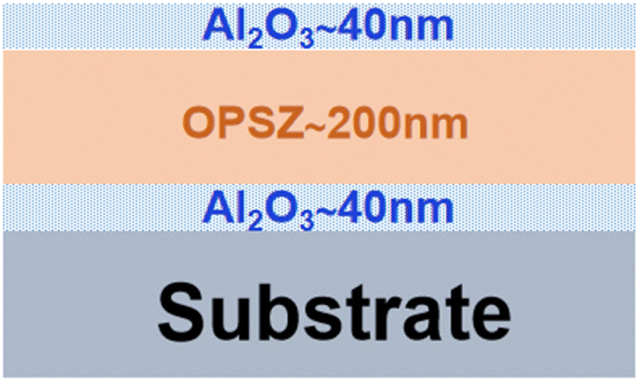 | ||
| Fig. 1 Schematic of the multilayer barrier film. | ||
2.2 Characterization of the barrier films
The microstructures of the films at varying preparation steps were characterized by applying a Scanning Electron Microscope (SEM, Nova NanoSEM 450, FEI Company). The surface morphology of the OPSZ prepared at different rotation speeds was captured using a 3D laser scanning microscope (VK-X1000, Keyence). The surface contact angle of the films was determined using a contact angle meter (DSA100, KRUSS). The surface elemental composition was measured using energy-dispersive X-ray spectroscopy (EDS) and X-ray photoelectron spectroscopy (XPS) (Escalab 250Xi, Thermo Scientific). The cross-sectional morphology of the film was observed using a Transmission Electron Microscope (TEM, JEM ARM200F, JEOL). Before TEM imaging, site-specific milling was performed by applying the focused ion beam (FIB) technique. The surface morphology and roughness of the films were evaluated using atomic force microscopy (Dimension ICON, Bruker). The optical transmittance of the films was measured using a spectrophotometer (UV-3600, Shimadzu) in the wavelength range of 400–1200 nm. The WVTR of the films with a sample size of about 10 cm × 10 cm was obtained using MOCON Aquatran 3 (Aquatran model 3, MOCON Inc., USA) at 38 °C and 90% relative humidity (RH). The fatigue tensile test method was used to study the flexibility of the barrier films. The number of tensile cycles was 100, and the tensile strain increased from 1% to 5%. In the bending test, the bending strain is calculated from the bending radius of the film. The formula is as follows: ε = (t1 + t2)/2r, where t1 and t2 are the thicknesses of the substrate and coating, respectively, and r is the bending radius. An ultra-depth 3D microscope (DSX510, OLYMPUS) was used to observe the changes in the surface topography of the samples.3. Results and discussion
3.1 Microscopic morphology of the Al2O3 layer
In this work, Al2O3 layers were deposited by PEALD at 120 °C.27 Fig. 2(a) shows the surface SEM image of the first Al2O3 layer deposited on the PEN substrate. The Al2O3 layer shows a homogeneous, smooth surface. Fig. 2(b) shows a cross-sectional SEM image of the PEN/Al2O3 film obtained after 350 ALD cycles. The Al2O3 layer thickness is about 44.7 nm, corresponding to an ALD growth rate of 0.124 nm per cycle. The number of ALD cycles was fixed at 350 for the Al2O3 layer deposition in the subsequent preparation of the Al2O3/OPSZ/Al2O3 multilayer barrier films.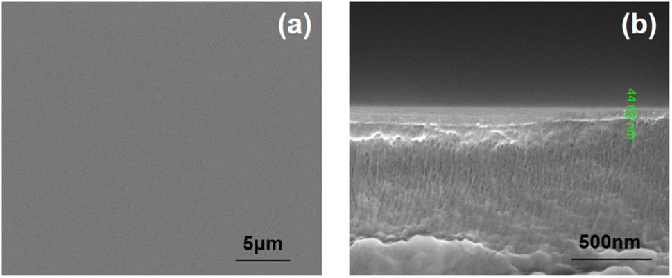 | ||
| Fig. 2 Surface (a) and cross-sectional (b) SEM images of the Al2O3 film. | ||
3.2 Microscopic morphology of the OPSZ layer
The spray-spin coating method was used to prepare the nano-scale OPSZ layer. To determine the optimum coating conditions, OPSZ layers were first prepared on a PEN substrate by varying the rotation speed in the range of 500–5000 rpm. A 3D laser scanning microscope was used to investigate the uniformity of the OPSZ films. As shown in Fig. 3(A)–(D), the OPSZ layer prepared with a rotation speed of 5000 rpm yields the smoothest surface. Besides, the thickness of the OPSZ layer decreases as the rotation speed increases, and the downward trend in film thickness levels off at rotation speeds above 3000 rpm. When the rotation speed reaches 5000 rpm, the thickness of the OPSZ layer is evaluated to be about 210 nm (Fig. 3(d)). A rotation speed of 5000 rpm was used in the subsequent spray-spin coating preparation of the OPSZ layer in the multilayer films.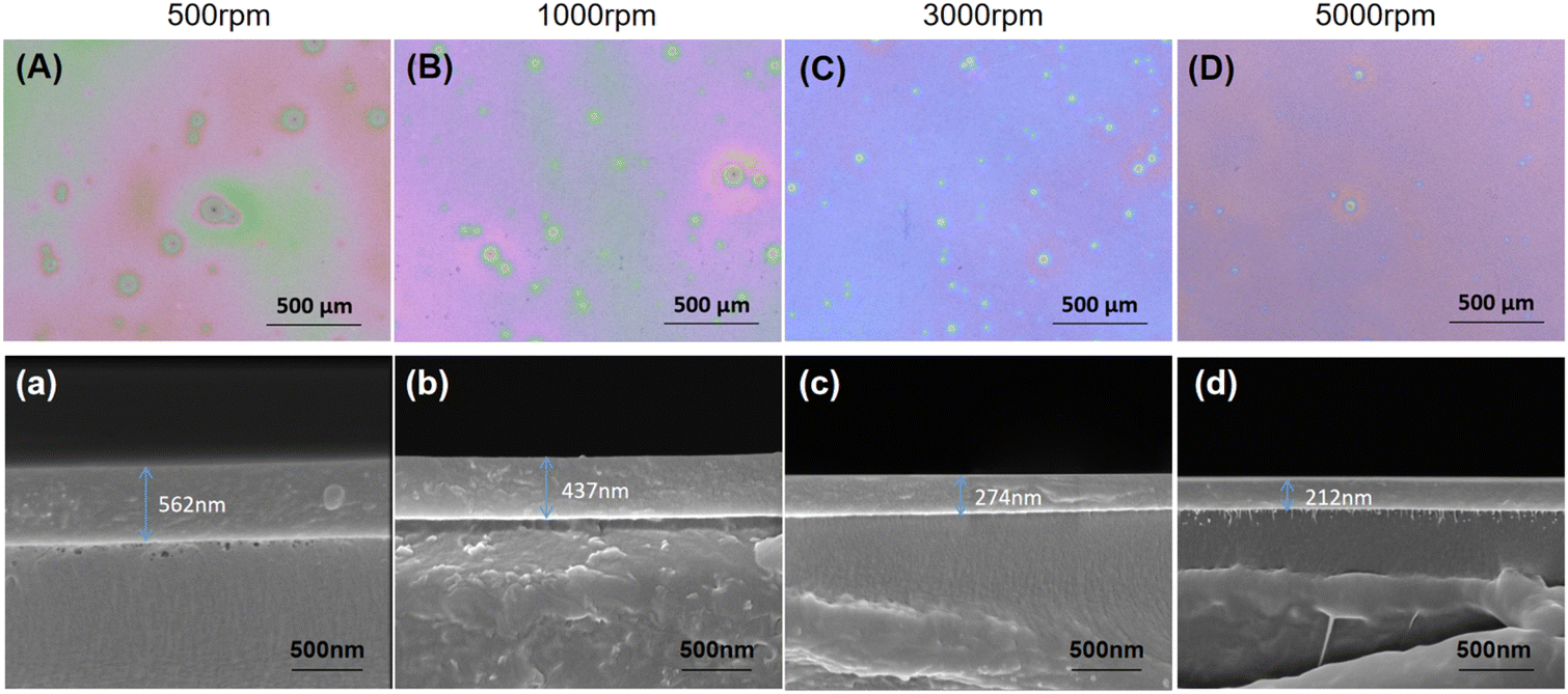 | ||
| Fig. 3 Optical microscope images (A)–(D) and SEM cross-sectional images (a)–(d) of OPSZ layers on PEN substrate. | ||
3.3 Changes in PEN/Al2O3/OPSZ film surface with plasma treatment
OPSZ layer was coated on the surface of PEN/Al2O3 film. The prepared PEN/Al2O3/OPSZ film was then cured at 80 °C for 2 hours before plasma treatment. Water contact angle (WCA) measurements were taken on the as-cured and plasma treatment films. Fig. 4(a) shows that the OPSZ layer before plasma treatment shows a generally hydrophobic character with a contact angle of around 93°. In general, hydrophobic surfaces have low surface energy,28 which is not conducive to nucleation during PEALD.29,30 As shown in Fig. 4(b), a contact angle of around 0° is observed, indicating that a complete wetting surface has been achieved after O2 plasma treatment. Fig. 4(c)–(f) further shows the effect of storage time on the WCA values on the OPSZ surface; the plasma-treated PEN/Al2O3/OPSZ film retains relative hydrophilicity after 7 days of storage time. It is thus demonstrated that plasma treatment is an effective protocol for rendering a hydrophilic surface and providing nucleation sites for the ALD process.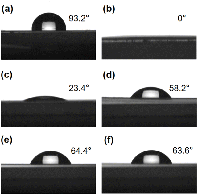 | ||
| Fig. 4 Images of contact angle before (a) and after (b)–(f) plasma treatment: 0 day (b), 1 day (c), 3 days (d), 5 days (e), and 7 days (f) storage time after treatment. | ||
Fig. 5 shows the surface elemental compositions of films containing as-cured OPSZ layers measured by Energy Dispersion Spectroscopy (EDS). After plasma treatment, the oxygen content increases as shown in Fig. 5, indicating that oxygen-containing groups were introduced onto the surface of the OPSZ layer. The introduced functionalities improved the surface hydrophilicity. However, it is found that the increase in the oxygen element is relatively low. This is mainly because the plasma treatment is confined to only a few nanometers at the surface.
 | ||
| Fig. 5 EDS results of the OPSZ surface before (a) and after (b) plasma treatment. | ||
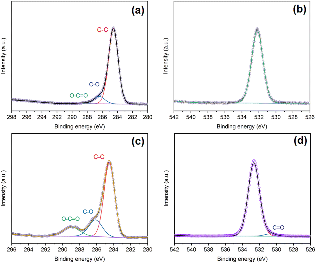
Fig. 6(a) and (c) show the C 1s high-resolution spectra of the OPSZ surface before and after plasma treatment, respectively. Compared with untreated OPSZ, plasma-treated OPSZ surface shows increased C–O and O–C![[double bond, length as m-dash]](https://www.rsc.org/images/entities/char_e001.gif) O/C–C ratios. Fig. 6(b) and (d) compare the O 1s high-resolution spectra of the OPSZ surface before and after treatment, respectively. A peak of OC (530.7 eV) is detected in the treated OPSZ surface. Simultaneously, the binding energy of O 1s shifts from 532.2 eV to 532.6 eV, suggesting the presence of hydroxyl groups. The above analysis indicates that oxygen containing groups, such as O–CO, C–O, and OH, have been successfully introduced on the OPSZ surface after the treatment.
O/C–C ratios. Fig. 6(b) and (d) compare the O 1s high-resolution spectra of the OPSZ surface before and after treatment, respectively. A peak of OC (530.7 eV) is detected in the treated OPSZ surface. Simultaneously, the binding energy of O 1s shifts from 532.2 eV to 532.6 eV, suggesting the presence of hydroxyl groups. The above analysis indicates that oxygen containing groups, such as O–CO, C–O, and OH, have been successfully introduced on the OPSZ surface after the treatment.
 | ||
| Fig. 6 C 1s and O 1s spectra of the OPSZ surface before (a) and (b) and after (c) and (d) plasma treatment. | ||
3.4 Structure and properties of Al2O3/OPSZ/Al2O3 film
Fig. 7 shows a HRTEM image of the Al2O3/OPSZ/Al2O3 film on the PEN substrate. The film consists of a 44.76 nm-thick Al2O3 layer, a 207.58 nm-thick OPSZ layer and another 43.12 nm-thick Al2O3 layer. The interfaces of PEN/Al2O3 and OPSZ/Al2O3 layers are well-defined. It is known that grain boundaries in crystalline layers are potential pathways for water vapor diffusion. Notably, the Al2O3 thin layer displays a continuous, homogeneous, and amorphous structure, minimizing the pathways for water permeating. From the mapping images, it is clearly observed that the Al and Si elements are uniformly distributed within the Al2O3 and OPSZ layers, respectively. The O element is distributed throughout the whole barrier film, while the C element is mainly distributed in the OPSZ layer. Both Au and Pt elements are artificially plated to protect the sample surface.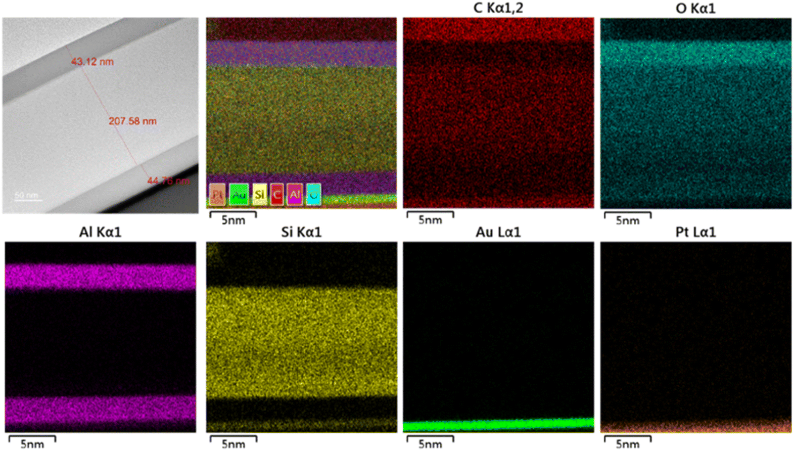 | ||
| Fig. 7 HRTEM cross-sectional image and EDS mapping of the Al2O3/OPSZ/Al2O3 three-layer barrier film. | ||
The surface smoothness of the bare PEN and different barrier films is measured by AFM over a scanned area of 5 μm × 5 μm. As shown in Fig. 8, the average surface roughness (Ra) for bare PEN is 1.25 nm. Upon deposition of the first Al2O3 layer, the surface roughness of the PEN/Al2O3 film decreases noticeably to 0.59 nm. Coating the OPSZ layer onto the above film results in further surface smoothing (Ra = 0.46 nm) (Fig. 8(c)). Thus, both the Al2O3 and OPSZ layers contribute to roughness reduction, which is conducive to the growth of a dense and pinhole-free Al2O3 surface layer of the multilayer barrier film. As expected, the subsequent Al2O3/OPSZ/Al2O3 barrier film shows a desired minimal Ra of 0.38 nm (Fig. 8(d)).
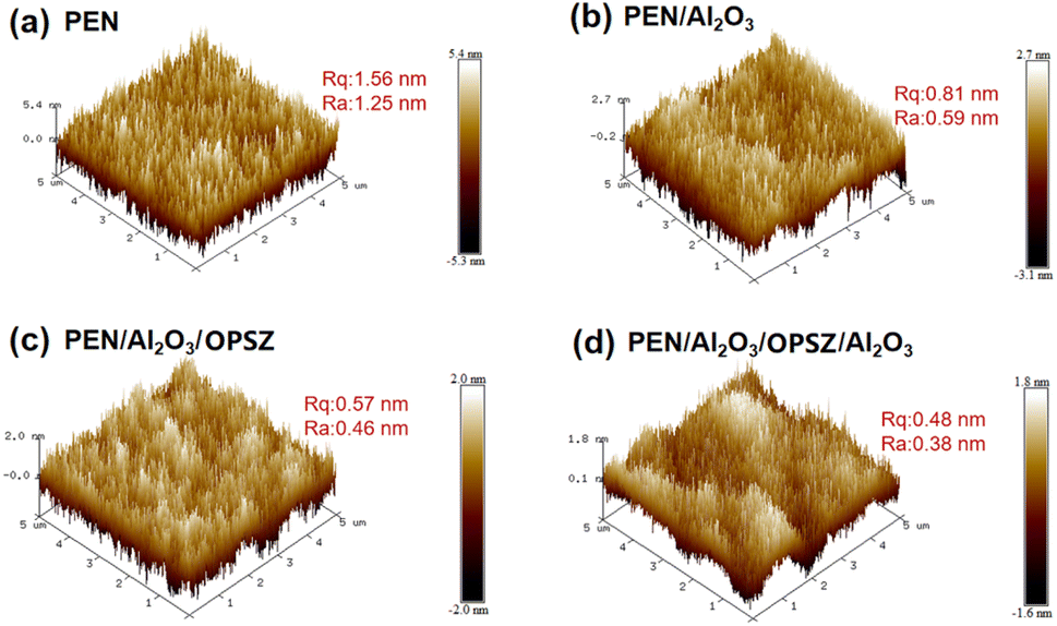 | ||
| Fig. 8 AFM images and surface roughness values of (a) PEN, (b) PEN/Al2O3, (c) PEN/Al2O3/OPSZ, and (d) PEN/Al2O3/OPSZ/Al2O3. | ||
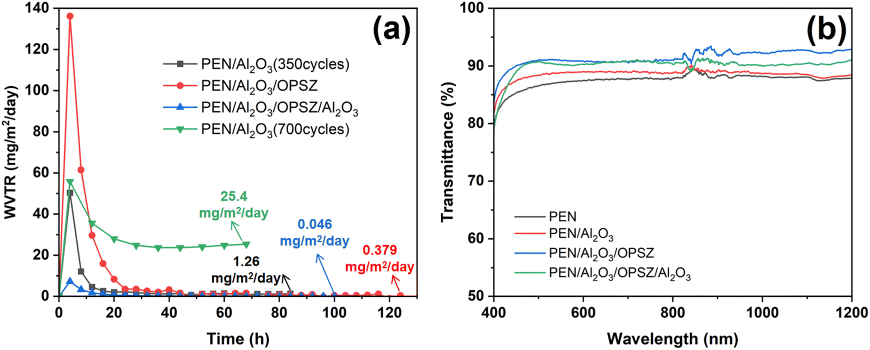
The WVTR was measured using MOCON Aquatran 3 to investigate the barrier properties of the films with regards to moisture. Unlike the small sample size of the Ca test, the size of the sample tested on MOCON equipment is as large as 10 cm × 10 cm. The WVTR for the pristine PEN substrate film is measured to be 1.3 g per m2 per day, which is consistent with the reported results.31 As shown in Fig. 9(a), the 350-cycle deposited PEN/Al2O3 thin film exhibits a WVTR value of 1.26 × 10⁻³ g per m2 per day. As the deposition cycles increase to 700, the WVTR value of the PEN/Al2O3 film increases to 2.54 × 10⁻² g per m2 per day. The increased WVTR value could be ascribed to the propagation of defects. The introduction of an OPSZ layer on PEN/Al2O3 leads to a sharply decreased WVTR value (3.79 × 10⁻⁴ g per m2 per day). Finally, after the ALD deposition of an additional layer of Al2O3, the multilayer film exhibits the lowest WVTR value of 4.6 × 10⁻⁵ g per m2 per day, which is 2–3 orders of magnitude lower than that of a single Al2O3 film.
 | ||
| Fig. 9 WVTR values (a) and optical transmittance (b) of different barrier films. | ||
Optical properties are extremely important for barrier film for flexible devices. Normally, a light transmittance of higher than 90% is required for flexible electronic device encapsulation.32 The optical transmittance as a function of wavelength for different barrier structures was measured by applying a UV-visible spectrophotometer, and the transmittance spectra are shown in Fig. 9(b). PEN/Al2O3/OPSZ and multilayer films show average transmittance values of 91.4% and 90.1% between 400 and 1200 nm wavelengths, respectively, which are more transparent than those of bare PEN substrate (Tr 87.5%) and PEN/Al2O3 film (Tr 88.5%). This demonstrates that the introduction of the OPSZ polymer layer can effectively prevent light scattering owing to its lower surface roughness, resulting in a higher transmittance of the multilayer films.
A schematic illustration of the reduced WVTR of the multilayer film compared to the neat Al2O3 film is presented in Fig. 10. First, the introduction of the OPSZ layer can help to achieve a flattened surface.33 Meanwhile, the organic layer is known to decouple defects in Al2O3 layers, thereby preventing direct penetration through defect sites. Moreover, diffusion lag times are remarkably extended with a prolonged diffusion path of water vapor permeation owing to the presence of an organic layer sandwiched between the two Al2O3 inorganic layers.34 Consequently, the Al2O3/OPSZ/Al2O3 multilayer film achieves significant barrier properties compared to the film made solely of Al2O3.
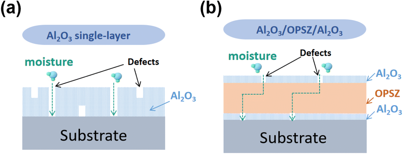 | ||
| Fig. 10 Schematic of the diffusion of water vapor through the Al2O3 single-layer (a) and Al2O3/OPSZ/Al2O3 multilayer (b) films. | ||
Tensile and bending strain measurements for 100 cycles are used to test the flexibility of barrier films. Fig. 11 shows that obvious cracks can be observed in the Al2O3 single-layer film when stretched at 5% strain, while no cracks are observed in the Al2O3/OPSZ/Al2O3 multilayer film with the applied strain from 1% to 5%. A bending test is performed with strains of 1.3%, 1.8%, 2.5%, and 3%. From Fig. 12, it can be observed that neither Al2O3 single-layer nor Al2O3/OPSZ/Al2O3 multilayer films show cracks at a low bending strain. Until the strain reaches 3%, cracks appear in the Al2O3 single-layer film. The above analysis indicates that the organic layer is advantageous for promoting the flexibility of barrier films. Therefore, the tensile and bending resistance of the Al2O3/OPSZ/Al2O3 multilayer film is better than that of the Al2O3 single-layer film.
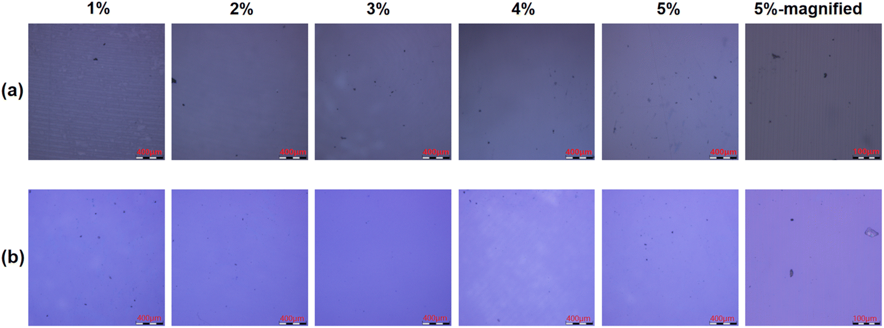 | ||
| Fig. 11 Microscopic images for Al2O3 single-layer (a) and Al2O3/OPSZ/Al2O3 multilayer (b) films after 1%, 2%, 3%, 4%, and 5% tensile strain. | ||
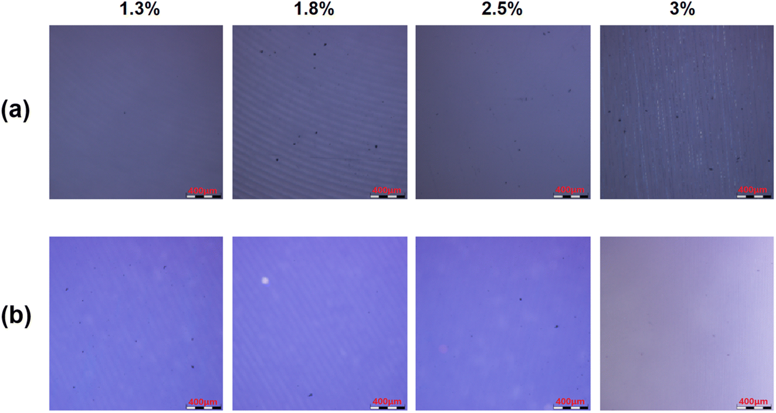 | ||
| Fig. 12 Microscopic images for Al2O3 single-layer (a) and Al2O3/OPSZ/Al2O3 multilayer (b) films after 1.3%, 1.8%, 2.5%, and 3% bending strain. | ||
The Al2O3/OPSZ/Al2O3 barrier film has potential value and wide application prospects in many industries, especially OLED and solar photovoltaic module encapsulation, which require a very high barrier grade for the encapsulation film. Furthermore, Al2O3 coatings have been used in a wide range of food packaging and bio-applications owing to their antibacterial and biocompatibility properties.35,36 The Al2O3/OPSZ/Al2O3 barrier film, owing to its superior barrier performance, has greater potential for application in these fields.
4. Conclusions
In summary, Al2O3/OPSZ/Al2O3 multilayer barrier film on a 10 cm × 10 cm large-area PEN substrate is prepared using PEALD and spray-spin coating processes. The effects of fabrication parameters, layer number, and layer interaction on optical properties and microstructure are investigated systematically. Consequently, the fabricated multilayer film shows a smooth surface characteristic with a minimal Ra of 0.38 nm. Ultra-low WVTR value (4.6 × 10⁻⁵ g per m2 per day, at 38 °C, 90% RH), high optical transmission (>90%), and good tensile and bending resistance are achieved. Thus, this work demonstrates that the fabricated multilayer structure barrier films possess great potential for the encapsulation of flexible devices.Data availability
The raw data supporting the conclusions of this article will be made available by the authors upon request.Author contributions
X. J. Sun: conceptualization, methodology, validation, formal analysis, investigation, writing—original draft preparation; W. Feng: writing-review and editing, supervision, project administration.Conflicts of interest
There are no conflicts to declare.Acknowledgements
This work was financially supported by the National Natural Science Foundation of China (Grant No. 52327802).References
- B. H. Kwon, H. Lee, M. Kim, C. W. Joo, H. Cho, J. T. Lim and Y. S. Jung, J. Ind. Eng. Chem., 2021, 93, 237–244 CrossRef CAS.
- Y. Li, K. Cao, Y. Xiong, H. Yang, Y. Zhang, Y. Lin, B. Zhou, J. Huang and R. Chen, Adv. Mater. Interfaces, 2020, 7, 2000237 CrossRef CAS.
- Y. Weng, G. Chen, X. Zhou, Y. Zhang, Q. Yan and T. Guo, ACS Appl. Polym. Mater., 2023, 5, 10148–10157 CrossRef CAS.
- S. U. Shin and S. O. Ryu, J. Electron., 2021, 50, 2015–2020 CAS.
- K. Y. Lim, H. H. Kim, J. H. Noh, S. H. Tak, J.-W. Yu and W. K. Choi, RSC Adv., 2022, 12, 4113–4119 RSC.
- J. S. Park, H. Chae, H. K. Chung and S. I. Lee, Semicond. Sci. Technol., 2011, 26, 034001 CrossRef.
- Q. Lu, Z. Yang, X. Meng, Y. Yue, M. A. Ahmad and W. Zhang, Adv. Funct. Mater., 2021, 31, 2100151 CrossRef CAS.
- Y. Weng, G. Chen, X. Zhou, Y. Zhang, Q. Yan and T. Guo, ACS Appl. Polym. Mater., 2023, 5, 10148–10157 CrossRef CAS.
- J. S. Lewis and M. S. Weaver, IEEE J. Sel. Top. Quantum Electron., 2004, 10, 45–57 CrossRef CAS.
- R. Q. Ma, R. Hewitt, K. Rajan, J. Silvernail, K. Urbanik, M. Hack and J. J. Brown, J. Soc. Inf. Disp., 2008, 16, 169–175 CrossRef.
- Y. Leterrier, D. Pellaton, D. Mendels and R. Glauser, J. Mater., 2001, 36, 2213–2225 CAS.
- Y. Li, Y. Xiong, H. Yang, K. Cao and R. Chen, J. Mater., 2020, 35, 681–700 CAS.
- S. Lee, Y. Jeon, S. J. Oh, S.-W. Lee, K. C. Choi, T.-S. Kim and J. H. Kwon, Mater. Horiz., 2023, 10, 4488–4500 RSC.
- S. J. Oh, S.-W. Lee, H. Lee, H. Kim, T.-S. Kim and J. H. Kwon, Adv. Mater. Technol., 2024, 9, 2400381 CrossRef CAS.
- M. Li, M. Xu, J. Zou, H. Tao, L. Wang, Z. Zhou and J. B. Peng, Nanotechnology, 2016, 27, 494003 CrossRef PubMed.
- J. Meyer, P. Görrn, F. Bertram, S. Hamwi, T. Winkler, H.-H. Johannes, T. Weimann, P. Hinze and P. Hinze, Adv. Mater., 2009, 21, 1845–1849 CrossRef CAS.
- A. Bulusu, A. Singh, C. Y. Wang, A. Dindar, C. Fuentes-Hernandez, H. Kim, D. Cullen, B. Kippelen and S. Graham, J. Appl. Phys., 2015, 118, 085501 CrossRef.
- Y. Duan, Y. Q. Yang, Z. Chen, Y. Tao and Y. F. Liu, Opt. Commun., 2016, 362, 43–44 CrossRef.
- P. F. Carcia, R. S. McLean and M. H. Reilly, Appl. Phys. Lett., 2006, 89, 031915 CrossRef.
- M. S. Weaver, L. A. Michalski, K. Rajan, M. A. Rothman, J. A. Silvernail and J. J. Brown, Appl. Phys. Lett., 2002, 81, 2929–2931 CrossRef CAS.
- S. H. Jen and S. M. George, ACS Appl. Mater., 2013, 5, 1165–1173 CrossRef CAS PubMed.
- J. Parka, J. Setha, S. Chob and M. M. Sung, Appl. Surf. Sci., 2020, 502, 144109 CrossRef.
- L. Sun, Y. Kurosawaa, H. Itob, Y. Makishimab, H. Kitab, T. Yoshidac and Y. Suzuri, Org. Electron., 2019, 64, 176–180 CrossRef CAS.
- P. van de Weijer, P. C. P. Bouten, S. Unnikrishnan, H. B. Akkerman, J. J. Michels and T. M. B. v. Mol, Org. Electron., 2017, 44, 94–98 CrossRef CAS.
- X. Wang, Y. H. Duan, Z. Chen, Y. Duan, Y. Q. Wang and P. Chen, Nanoscale Res. Lett., 2015, 10, 130 CrossRef PubMed.
- S. A. Mahadik, F. Pedraza and S. S. Mahadik, Prog. Org. Coat., 2017, 104, 217–222 CrossRef CAS.
- Y. Q. Ren, X. J. Sun, L. L. Chen, H. Wei, B. Feng and J. Y Chen, RSC Adv., 2023, 13, 3766–3772 RSC.
- E. J. Falde, S. T. Yohe, Y. L. Colson and M. W. Grinstaff, Biomaterials, 2016, 104, 87–103 CrossRef CAS PubMed.
- N. Y. Garces, V. D. Wheeler and D. K. Gaskill, J. Vac. Sci. Technol. B., 2012, 30, 030801 CrossRef.
- W. C. Shin, J. H. Bong, S. Y. Choi and B. J. Cho, ACS Appl. Mater., 2013, 5, 11515–11519 CrossRef CAS PubMed.
- K. L. Jarvis, P. J. Evans and G. Triani, Surf. Coat. Technol., 2018, 337, 44–52 CrossRef CAS.
- Q. Q. Chu, Z. Sun, D. Wang, B. Cheng, H. Wang, C. P. Wong and B. Fang, Matter, 2023, 6, 3838–3863 CrossRef CAS.
- H. G. Kima, J. G. Leea and S. S. Kim, Org. Electron., 2018, 52, 98–102 CrossRef.
- N. Kim, W. J. Potscavage Jr, A. Sundaramoothi, C. Henderson, B. Kippelen and S. Graham, Sol. Energy Mater. Sol. Cells., 2012, 101, 140–146 CrossRef CAS.
- V. Dias, H. Maciel, M. Fraga, A. C. Lobo, R. Pessoa and F. R. Marciano, Materials, 2019, 12, 682 CrossRef CAS PubMed.
- J.-H. Eom, T.-Y. Cho and S.-K. Cho, Appl. Surf. Sci., 2023, 638, 158011 CrossRef CAS.
| This journal is © The Royal Society of Chemistry 2025 |