Efficiency boost in perovskite solar cells via TiO2 nanodiscs embedded in the MoSe2 electron transport layer revealed by optoelectronic simulations†
Received
11th October 2024
, Accepted 17th February 2025
First published on 20th February 2025
Abstract
To improve the performance of inverted perovskite solar cells (IPSCs), we introduce a novel approach to enhance the devices' efficiency notably using the Finite Element Method (FEM). Our novel strategy incorporates a cutting-edge metasurface-based reflector featuring titanium dioxide (TiO2) nanodiscs within a MoSe2 layer, employed as an electron transport layer (ETL). Demonstrating a substantial improvement in light reflection from the lower part of the structure, the TiO2 nanodiscs as a metasurface-based reflector enhance electron transfer. Notably, the metasurface-based perfect reflector, incorporating TiO2 nanodiscs, outperforms other TiO2 nanocube variations with an impressive light reflectance of 97.95%. Exploring different materials for ETLs and hole transfer layers (HTLs), we identify molybdenum diselenide (MoSe2) as a potent secondary absorbent material, featuring a smaller bandgap than the primary absorbent CH3NH3PbI3 (MAPbI3), thereby intensifying the electric field within the active layer and improving Power Conversion Efficiency (PCE). In the final evaluation, our inverted metasurface-based device structure (indium tin oxide (ITO)/cuprous oxide (Cu2O)/MAPbI3/TiO2 nanodiscs and MoSe2/aluminum (Al)/silicon dioxide (SiO2)) significantly enhances the solar cell's electrical characteristics compared to the planar reference structure (ITO/copper(I) thiocyanate (CuSCN)/MAPbI3/TiO2/Al), with noteworthy increases in short circuit current density (Jsc), open circuit voltage (Voc), and PCE values from 17.98 mA cm−2 to 21.91 mA cm−2, 1.03 V to 1.07 V, and 15.33% to 19.17%, respectively. This comprehensive investigation underscores the promising potential of our proposed inverted metasurface-based device structure for advancing solar cell technology.
1. Introduction
The increasing demand for clean energy has become a critical issue due to the shortage of fossil fuel resources, the resulting air pollution, and the urgent need for immediate action to combat climate change.1–3 Therefore, the rapid development of new energy harvesting technologies to provide alternative clean, renewable, and sustainable energy from natural sources, such as solar—the most abundant energy resource—is crucial.4–7 In recent years, perovskite solar cells have achieved significant advancements, including higher PCE and lower manufacturing costs compared to the market-dominant silicon solar cells.8–11 Perovskite materials find application in diverse single-junction and tandem solar cell architectures, both for indoor and outdoor environments.12–16 Among all different subgroups of perovskites, there has been extensive interest on metal halide perovskite solar cells. This is widely because of their remarkable optical and electrical properties such as noticeably high light absorption spectrum, simple fabrication processes, and substantial carrier mobility and diffusion lengths.17,18 The selection of MAPbI3 is driven by the abundance of research literature and datasets, enabling a data-driven approach to model building.19–22 Therefore, MAPbI3 was used as the perovskite active layer in this work due to the wide light absorption spectra (wavelengths region including 300 to 800 nm) and proper carrier transfer (high carrier mobility and permittivity).23–25 In order to enhance the solar cell's PCE, metasurface structures were developed to manipulate the incoming incident light.26–28 Furthermore, metasurface structures are easy to fabricate and have proven to increase the light absorption because of the internal light reflections that cause light interactions with other layers.29,30 Thus, deploying this technology in solar cell devices has raised attention and is currently used by many researchers.31–34 The integrated periodic nanostructured metasurfaces perform mainly through the Snell's law by trapping the incident light and inclining the total absorption of the solar cell.35,36 Therefore, opting the material, shape and size of the nanostructure have serious consequence in the system's efficiency.37–40 The TiO2 nanodiscs can be grown on an Al substrate using a hydrothermal technique involving several steps.41,42 A research on a nanostructured cubic metasurface reflector consisting of three layers of TiO2/Ag/SiO2 proved to have a promising performance.43 Therefore, in this paper, different shapes (nanodiscs and three various types of nanocubes) of TiO2 were selected as the integrated metasurface nanostructure and the ETL on top of a planar Al/SiO2 structure to reach the optimized structure. Then, the nanostructure's size and position's degrees were optimized for one of the nanocubic structures to reach the highest light reflection to increase the total light absorption of the solar cell. However, the light reflection was further improved by using TiO2 nanodiscs instead. In order to increase the light reflection by the metasurface nanostructure, another optical study was done on discovering the material with suitable refractive index to surround the TiO2 nanostructure. Thereby, ETL materials such as zinc oxide (ZnO), Al-doped zinc oxide (AZO), cerium oxide (CeO2), and titanium dioxide–graphene (5%) (TiO2–Graphen (5%) or TiGO-5) were studied. Plus, this is a well-recognized issue that TiO2 only absorbs the visible light with the wavelength range of 300 to almost 400 nm.44 With regard to this, it can be argued that an inverted solar cell would be more beneficial to increase the total light reflection inside the device since the TiO2 nanostructure would be placed on a non-transparent contact like Al, which results in more light interaction in the ETL and consequently other layers. The IPSCs have become prominent in light of their advantageous characteristics like high stability and PCE.45,46 They consist of a reversed architecture, where the ETL and HTL are replaced by each other.47 Hence, the HTL material was required to have a low light absorption rate in order for the incident light to reach the active layer and the ETL as well. For this reason, different materials including CuSCN, Spiro-OMeTAD, copper(I) iodide (CuI), and CuO2 were studied as HTL. Additionally, another active layer, MoSe2, was used to enhance the light absorption, which was located below the MAPbI3 layer. MoSe2 exhibits a compelling set of properties that make it a promising candidate for integration into perovskite solar cells.48 Notably, its high electron mobility facilitates efficient charge transport, minimizing energy losses and boosting overall efficiency.49,50 Furthermore, MoSe2 offers tunable electrical characteristics, allowing for precise energy level alignment within the perovskite layer, crucial for optimal charge transfer.51 Its strong light absorption across the visible and near-infrared spectrum maximizes the utilization of solar energy, while its robust chemical and thermal stability ensure long-term device performance and reliability under diverse operating conditions.52 Finally, the layered structure of MoSe2 aligns well with the architecture of perovskite solar cells, potentially simplifying integration and enabling facile exfoliation for device fabrication.53 Finally, the results were compared to reach the optimized device with the highest PCE, resulted in the improvement in values of Jsc, Voc, and PCE from 17.98 mA cm−2 to 21.91 mA cm−2, 1.03 V to 1.07 V, and 15.33% to 19.17%, respectively.
2. Theory
In this section, the electrical and optical models and their coupling were discussed. Additionally, the simulation details related to these models were also described.
2.1. Optoelectronic model
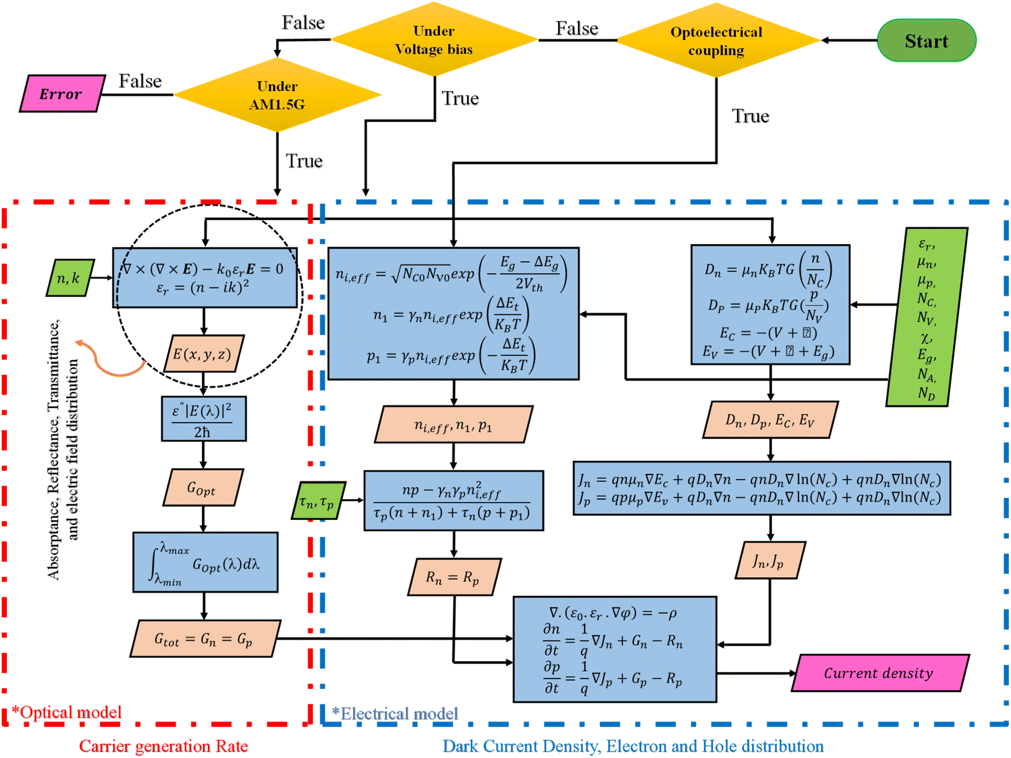
Two different sets of optical and electrical equations were analyzed in order to calculate various parameters, as shown in Fig. 1. The optical equations utilized Maxwell's equation (eqn (1)) to determine the electric field (E) with the input parameters including: refractive index (n) and extinction coefficient (k) of all layers.| | | ∇ × (∇ × E) − k0εrE = 0 | (1) |
 |
| | Fig. 1 Flowchart of the optoelectronic model to calculate solar cell parameters, where the red and blue sections are considered as separated optical and electrical models, respectively. In the optical model, the Maxwell's equation is solved to reach the carrier generation rate, whereas in the electrical model, the Poisson's and Continuity equations are solved to achieve the dark current density. The coupling of two models results in the photocurrent density of the solar cell. | |
The calculation of the electric field resulted in the optical outputs such as reflection, absorption, and the optical generation rate for electrons and holes (Gn, Gp). The optical generation rate referred to the number of the generated electron–hole pairs at each point in the device due to the absorption of photons.
The dark current density and electron–hole distribution and recombination rate of electron and hole (Rn, Rp) was then calculated by solving the Poisson's and Continuity equations (eqn (2)–(4)), as well as the related equations to Shockley–Reed–Hall (SRH) recombination by applying the input parameters such as band gap (Eg), electron affinity (χ), dielectric constant (ε), electron mobility (μn), hole mobility (μp), density state of valence band (NV), density state of conduction band (NC), acceptor and donor doping (NA,ND), electron lifetime (τn), and hole lifetime (τp) of each layer.
| |  | (3) |
| |  | (4) |
The current density in the cell was solved by coupling the two sets of equations. Fig. 1 illustrates the flowchart of the optoelectronic model. A standard AM 1.5 with the light intensity of 100 mW cm−2 perpendicular to the surface was used as the incoming light source. Different layers behaved differently after interacting with the incoming electric field according to their n and k. The dark current density, which has a direct relation with the amount of SRH recombination in the system, is calculated by solving the electric model without considering the incident electric field. To calculate the Jsc, both optical and electrical physics were solved, simultaneously. In this study, the wavelength in the range of 300 to 1200 nm was swept with 20 nm steps, and the current density spectrum was calculated in terms of wavelength. A sum of current densities in the abovementioned wavelength range with 20 nm steps was added to the dark current density to calculate the total current density in terms of voltage. In addition to SRH recombination for the metal contact, surface recombination is also considered for the simulation. The surface recombination velocity is set at 1 × 107 cm s−1 for both electrons and holes.
2.2. Simulation details
The materials' complex refractive indices (n and k) are plotted in Fig. S3, S5† and 7g. Also, the electrical parameters of the solar cell's layers (ZnO, AZO, CeO2, TiO2–Graphen (5%) (TiGO-5), CuSCN, Spiro-OMeTAD, CuI, Cu2O, MAPbI3, TiO2, MoSe2), including: ε, NC, NV, μn, μp, χ, Eg, NA, ND, τn and τp are provided in Table 1.
Table 1 Electrical parameters for the used materials in the electrical model, where εr denotes the dielectric constant, NC and NV present the density states of conduction and valence bands, respectively, μn and μp show the electron and hole mobility, respectively, χ is the electron affinity, Eg is the band gap, NA and ND are the acceptor and donor doping, respectively, and τn and τp show the electron and hole lifetime, respectively
| Parameters |
ZnO |
AZO |
CeO2 |
TiGO-5 |
CuSCN |
Spiro-OMeTAD |
CuI |
Cu2O |
MAPbI3 |
TiO2 |
MoSe2 |
|
ε
r
|
9 |
9 |
9 |
7.3 |
10 |
3 |
12.5 |
7.5 |
6.5 |
9 |
7.29 |
|
N
C (cm−3) |
2.2 × 10¹⁸ |
2.2 × 10¹⁸ |
1 × 10²⁰ |
1 × 10¹⁹ |
1.79 × 10¹⁹ |
2.2 × 10¹⁸ |
2.8 × 10¹⁹ |
2 × 10¹⁹ |
1.6 × 10¹⁹ |
1 × 10¹⁹ |
9 × 10¹⁸ |
|
N
V (cm−3) |
1.8 × 10¹⁹ |
1.8 × 10¹⁹ |
2 × 10²¹ |
1 × 10¹⁹ |
2.51 × 10¹⁹ |
1.8 × 10¹⁹ |
1 × 10¹⁹ |
1 × 10¹⁹ |
5.4 × 10¹⁹ |
1 × 10¹⁹ |
9 × 10¹⁸ |
|
μ
n/μp (cm2 V−1 s−1) |
100/25 |
10/5 |
100/25 |
12/12 |
25/25 |
2 × 10⁻⁴/2 × 10−4 |
100/43.9 |
8600/200 |
50/50 |
20/10 |
25/100 |
|
χ (eV) |
4 |
4.4 |
3.5 |
4.24 |
1.7 |
2.2 |
2.1 |
3.4 |
3.93 |
4 |
4.32 |
|
E
g (eV) |
3.3 |
3.35 |
4.6 |
3.1 |
3.6 |
3.0 |
3.1 |
2.2 |
1.55 |
3.2 |
1.4 |
|
N
A (cm−3) |
— |
— |
— |
— |
5 × 10¹⁸ |
1 × 10¹⁸ |
1 × 10¹⁸ |
1 × 10¹⁸ |
1 × 10¹³ |
— |
— |
|
N
D (cm−3) |
1 × 10¹⁸ |
1 × 10¹⁸ |
1 × 10²¹ |
5 × 10¹⁸ |
— |
— |
— |
— |
— |
5 × 10¹⁸ |
3 × 10¹⁸ |
|
τ
n/τp (ns) |
0.03/0.03 |
0.03/0.03 |
5/2 |
2/2 |
5/5 |
0.1/0.1 |
3/3 |
3/3 |
8/8 |
5/2 |
2.4/2.4 |
| Ref. |
54
|
55
|
56 and 57 |
58–61
|
56
|
56 and 62 |
56 and 63 |
64 and 65 |
62 and 64 |
66
|
67
|
3. Results and discussion
3.1. Metasurface based reflector design
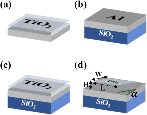
Fig. 2 shows the schematic of different types of structures in solar cells. The common inverted solar cell structures, as depicted in Fig. 2a, typically use bulk TiO2 as ETL on the contact. To enhance the reflection from the TiO2 surface, metasurface structures can be utilized. Unlike the natural behavior of materials, metasurface structures exhibit unique physical properties. Fig. 2b illustrates a reflector structure consisting of Al on SiO2 (as anti-reflection coating) substrate. Also, Fig. 2c shows the structure when the bulk TiO2 is applied on Al and SiO2. Finally, the schematic of the proposed metasurface unit cell consisting of TiO2 nanocubes on the Al and SiO2 substrate is presented in Fig. 2d. TiO2 is a preferred material for solar cell structures due to its high refractive index, smooth surface, and low heat loss, particularly in the visible region. The dimensions of the TiO2 nanocubes, including length (L), width (W), and height (H), are represented by specific parameters. Additionally, the angle of the nanocubes relative to the horizontal axis is shown with the parameter α. Based on the results, it can be argued that the use of TiO2 nanocubes on Al and SiO2 substrate can improve the efficiency of photonic structures and solar cells by enhancing the reflection from the TiO2 surface. The height of the Al and SiO2 substrate is 150 nm and 300 nm, respectively, while the length and width of the unit cell are both equal to 250 nm. Opting the mentioned dimensions serves two purposes: first, the unit cell's dimensions must be smaller than the incident wavelength, and second, the structure must be easily manufactured, particularly through electron beam lithography. The main objective of designing the proposed metasurface structure is to develop a reflector that reflects the transmitted light through the structure, to increase the total absorption in the structure.
 |
| | Fig. 2 (a) A common structure used as ETL in solar cells. (b) A reflector consisting of Al and SiO2. (c) The common structure of ETL in solar cells on SiO2 substrate. (d) TiO2/Al/SiO2 metasurface reflector structure. | |
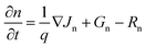
Each of the structures shown in Fig. 2 behaved differently to electromagnetic waves, and consequently, the amount of reflection from each structure varied. To increase the amount of reflectance from the reflector surface, various parameters, including H, L, W, and α were optimized. Therefore, the angle of the nanocube with the X-axis, represented by the parameter α, was swept from 0° to 70° with steps of 10° to. According to Fig. 3a and Table 2, a, and the incident power has the highest amount of reflection in the structure, reaching 91.57%, when the angle is 0°. The H, L and W parameters of the TiO2 nanocubes are also effective in determining the amount of reflectance of the structure. By examining different heights of nanocubes from 100 to 500 nm with steps of 100 nm, different results were obtained. As the height was increased, the amount of reflectance from the surface decreased, and the highest amount of reflectance from the structure was at H = 100 nm according to Table 2, b. This could be explained by the frequency shift in the reflectance spectrum, where it reached the highest amount of reflection in the wavelength range of 300 to 1200 nm at this height. The amount of reflectance was increased to 93.36% by optimizing the height, which is more efficient compared to when the angle was optimized, 91.57%. Then, the L parameter was varied from 90 nm to 210 nm with steps of 20 nm while keeping the angle and height constant at their optimized values. The best result was obtained at L = 190 nm, which increased the amount of reflection up to 94.47% compared to the height optimization. The ratio of L/W was considered equal to 15/9. The optimal dimensions of the TiO2 nanocubes were determined to be α = 0°, H = 100 nm, and L = 190 nm. By optimizing these parameters, the total reflectance of the structure in the wavelength range of 300 to 1200 nm reached a significant amount of 94.47%. The amount of reflection from the surface of the depicted structures in Fig. 2, is displayed in Fig. 3d. The metasurface structure exhibited a significant increase in reflectance compared to other structures, particularly the structure in Fig. 2a, which is commonly used in solar cells. According to Table 2, d, the amount of reflection in the wavelength range of 300 to 1200 nm in the provided metasurface structure in Fig. 2d was significantly increased from 78.08% to 94.47% compared to the given structure in Fig. 2a, which is commonly used in solar cells.
 |
| | Fig. 3 The reflectance spectrum in terms of wavelength in the range of 300 to 1200 nm for (a) different values of α (nanocubic angle with horizontal axis), while considering H = 300 nm, L = 150 nm, and W = 90 nm, (b) different values of H, while considering α = 0, L = 150 nm, and W = 90 nm, (c) different optimizations including three steps, (d) comparing the optimized metasurface structure with other structures in Fig. 2. | |
Table 2 Reflectance values for (a) different values of α considering H = 300 nm, L = 150 nm and W = 90 nm, (b) different values of H considering α = 0°, L = 150 nm and W = 90 nm, (c) different values of L considering α = 0°, H = 100 nm and L/W = 15/9, and (d) different provided structures in Fig. 2
| (a) |
|
H/L/W (nm) |
α° |
Reflectance (%) |
| 300/150/90 |
0 |
91.57 |
| 300/150/90 |
10 |
91.50 |
| 300/150/90 |
20 |
91.20 |
| 300/150/90 |
30 |
90.46 |
| 300/150/90 |
40 |
89.83 |
| 300/150/90 |
50 |
90.46 |
| 300/150/90 |
60 |
91.06 |
| 300/150/90 |
70 |
91.16 |
| (b) |
|
α°/L/W (nm) |
H (nm) |
Reflectance (%) |
| 0/150/90 |
100 |
93.36 |
| 0/150/90 |
200 |
92.97 |
| 0/150/90 |
300 |
91.57 |
| 0/150/90 |
400 |
91.11 |
| 0/150/90 |
500 |
91.81 |
| (c) |
|
α°/H (nm) |
L (nm) |
Reflectance (%) |
| 0/100 |
90 |
91.82 |
| 0/100 |
110 |
92.29 |
| 0/100 |
130 |
92.82 |
| 0/100 |
150 |
93.36 |
| 0/100 |
170 |
93.90 |
| 0/100 |
190 |
94.47 |
| 0/100 |
210 |
94.20 |
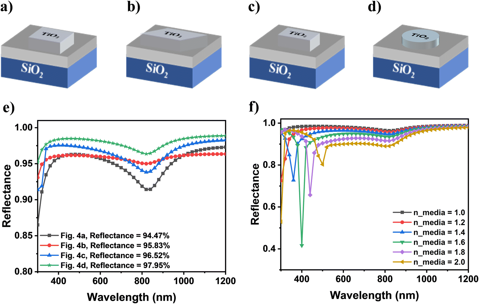
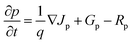
In order to enhance the light reflectance, other shapes of metasurface structures with TiO2 was further investigated. The depicted nanocubic structure in Fig. 2a, proved to reflect 94.47% of the incident light power. According to Fig. 4e, the provided structures in Fig. 4b–d shared higher values of light reflectance equal to 95.83%, 96.52%, and 97.95%, respectively. It was apparent that the TiO2 nanodiscs structure with the height of 100 nm and the diameter of 190 nm was selected as the most efficient structure for additional studies. Plus, the TiO2 nanodiscs have proven transfer electrons more effectively. Fig. 4e displays the reflectance diagram of the reflector structure in terms of wavelength in the range of 300 to 1200 nm, when using different types of nanocubes and nanodiscs as depicted in Fig. 4a–d. After rigorous examination, it was discovered that the materials' refractive indices, which surrounds the nanostructures, had a noticeable impact on the amount of the reflectance from the metasurface-based reflector structure. As illustrated in Fig. 4f, by changing the refractive index of the media around the TiO2 nanodiscs, the reflectance from the structure was changed. The investigated refractive index range was from 1 to 2 with steps of 0.2. According to the obtained results, the amount of reflection was higher in medias with lower refractive indices, which suggested that using materials with low refractive indices would results in more light absorption in the active layer of the solar cells. In conclusion, it can be claimed that photonic and metasurface nanostructures would improve the light absorption, ease fabrication, and improve efficiency in solar cells.
 |
| | Fig. 4 The schematic of the metasurface reflector nanostructure with (a–c) three different types of nanocubes and (d) nanodiscs. (e) The reflectance spectrum of the depicted nanostructures in (a–d). (f) The reflectance spectrum for the metasurface reflector considering different refractive indices values (1 to 2 with steps of 0.2) for the media around the TiO2 nanodiscs. | |
The purpose of designing the TiO2/Al/SiO2 reflector structure is to reflect light in order to reuse it in various applications such as solar cells and optical coatings. The combination of the mentioned materials allows for high reflectance at certain wavelengths. However, TiO2 has better reflective properties than other materials due to its higher dielectric constant, which leads to a higher refractive index and results in absorbing the incoming light less. Fig. S1† shows the electric field distribution of the reflector structure for three various wavelengths of 360, 500, and 740 nm. It should be pointed out that a metasurface-based reflector can exhibit resonance, when a surface is located around one of the coupled resonance frequencies. Resonance in metasurface reflectors can be reached through various methods. Moreover, it is used to achieve total reflection or design tunable metasurface unit cells. Fig. S1† depicts the three different resonances that occurred in different wavelengths, which can cause the electric field to intensify around and above the nanodiscs, leading to an increase in the total absorption of the solar cell (refer to the ESI† for more details).
3.2. Solar cell design
It is worth noting that the refractive index of the upper layer of TiO2 nanodiscs has an impact on the reflection spectra from this layer. To investigate this effect, the refractive index of this layer was swept from 1 to 4 with steps of 0.5, assuming the extinction coefficient to be equal to zero, which means no light absorption. By calculating the absorptance spectra from the surface of these layers, as provided in Fig. 5b, it was found that the refractive index range of 2 to 3 has the highest amount of light absorption in the structure. It is generally acknowledged that the enhancement in the reflectance spectra from the ETL can increase the light absorption in the active layer in an inverted solar cell. Plus, it prevents power loss by the metal contact. The finally proposed solar cell structure is presented in Fig. 5a. The structure is consisted of the following layers from top to bottom: ITO, HTL, active layer (MAPbI3), ETL including TiO2 nanodiscs and the other bulk material around these nanodiscs, Al, and SiO2. ITO was used as a transparent contact for light to pass through. The band diagram of the proposed solar cell in the presence of the metasurface reflector is illustrated in Fig. 5c. In this structure, ZnO was used as the material around the TiO2 nanodiscs, and CuSCN was used as the HTL. As plotted in Fig. 4f, the refractive index of the material around the TiO2 nanodiscs did not have a significant effect on the reflectance spectra. Therefore, a material featuring a better carrier transfer should be used along with TiO2, which can improve electron transfer, in addition to reflection improvement. According to Table 1, the MAPbI3 layer has an electron affinity of 3.93 eV and a bandgap of 1.55 eV, which can result in efficient light absorption in the wavelength range of 300 to 800 nm. On the ETL side, TiO2 and ZnO were used with the equal electron affinity value of −4 eV and the bandgap values of 3.2 eV and 3.3 eV, respectively. Due to the values of their conduction bands, these materials were able to transfer the electrons from the active layer into the Al contact with the work function of −4.3 eV. Furthermore, due to the values of their valence bands compared to MAPbI3, they prevented the holes from entering the Al contact conveniently. On the HTL side, CuSCN was used with a bandgap of 3.4 eV, which does not absorb a noticeable portion of light in the visible region. Therefore, most of the incident light was able to reach the active layer. CuSCN with an electron affinity of 1.9 eV was considered as a suitable barrier to prevent the electrons from entering the transparent contact (ITO) and transferred the generated holes in the active layer into the ITO side with a valence band energy level difference of 0.18 eV with MAPbI3.
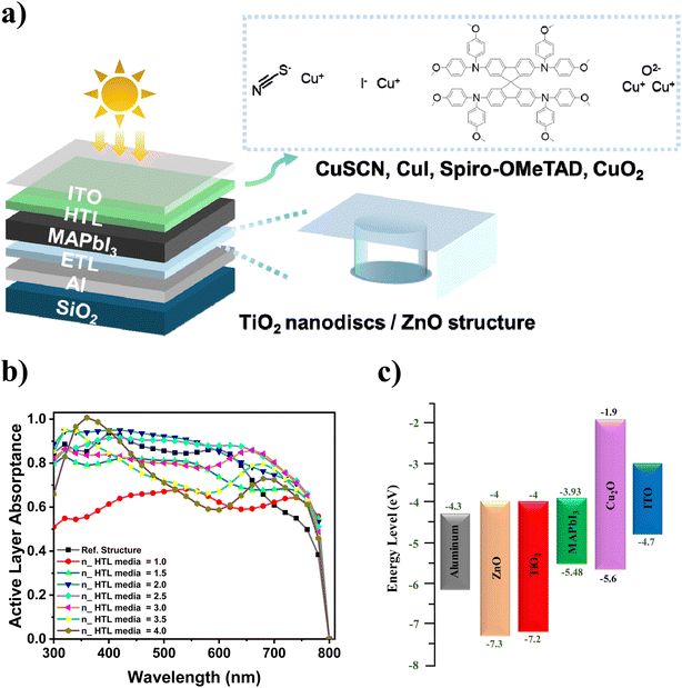 |
| | Fig. 5 (a) Schematic of the proposed solar cell with MAPbI3 as the active layer. (b) The active layer (MAPbI3) light absorptance spectrum with different HTL refractive indices between the range of 1 to 4 with steps of 0.5, while k = 0, and ZnO an TiO2 nanodiscs as ETL. (c) Band diagram of the proposed structure, considering ZnO as the material around the TiO2 nanodiscs, MAPbI3 as active layer, and CuSCN as the HTL (all energy levels depicted in this diagram are based on the values listed in Table 1). | |
It is obvious that applying different materials around TiO2 nanodiscs can affect the amount of electron transfer. Although, according to the findings pertinent to Fig. 4f, different refractive indices did not have a significant effect on the amount of light reflection, the light transmission of these materials was significant since they were not considered as absorbent materials. Therefore, various materials were considered for this purpose, including ZnO, AZO, CeO2, and TiGO-5. The refractive indices and extinction coefficients of these materials in terms of wavelength in the range of 300 to 800 nm are shown in Figs. S2.†
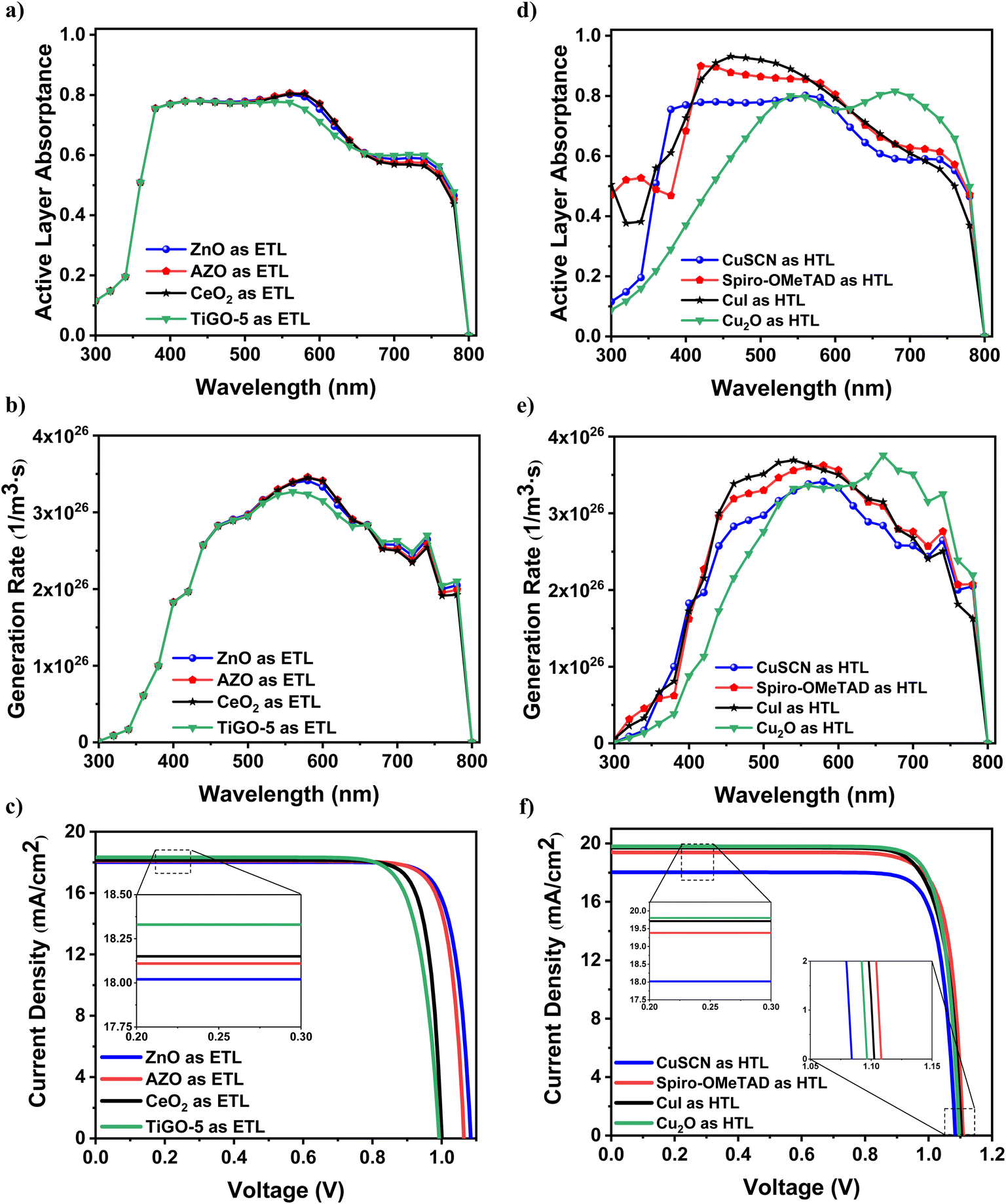
As demonstrated in Fig. 6a, the absorptance spectra of the active layer (MAPbI3) for different materials around the TiO2 nanodiscs did not change significantly in the wavelength range of 300 to 800 nm and is almost the same for different materials, including ZnO, AZO, CeO2, and TiGO-5. In order to generate electron–hole pairs, a photon with sufficient energy must be absorbed in the active layer. Therefore, the amount of carrier generation rate in different wavelengths, as depicted in Fig. 6b, is in accordance with the behavior of the absorptance diagram. Fig. 6c indicates the photocurrent density in terms of the voltage, where different values of the Voc, can be explained by the different electrical characteristics of the materials. Bearing in mind that ZnO has a higher electron mobility compared to other materials, as stated in Table 1, as well as the 0.3 eV difference in its conduction band energy compared to the Al work function, it resulted in a higher Voc value. Likewise, according to Table 1, AZO shared almost the same Voc value as ZnO due to their approximately equal electrical parameters. Despite ZnO and AZO, CeO2 showed a relatively lower Voc due to its lower conduction band than the Al work function. Similarly, TiGO-5 shared about the same Voc value to CeO2. This was because of the almost very close energy level of the TiGO-5 conduction band to the Al work function. The represented band diagram in Fig. S3† indicates that all the proposed materials as ETL can easily separate the electron from the active layer due to the lower energy level of their conduction band compared to the active layer's conduction band. Also, the holes were prevented to transfer into the metal contact in light of the same reason. It should be mentioned that the difference in Voc values is mainly contributed to the difference in the conduction band of these materials with the Al work function and also the electrical parameters of these materials according to Table 1.
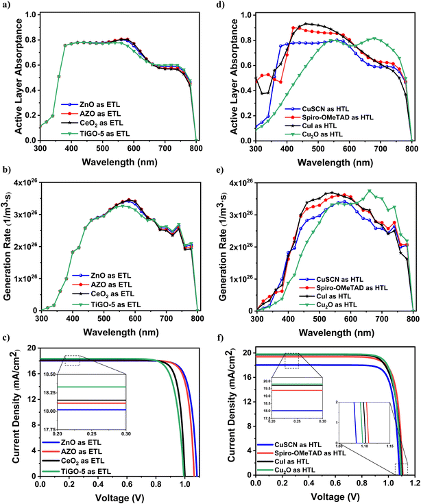 |
| | Fig. 6 The active layer (a) absorptance spectra, and (b) carrier generation rate in terms of wavelength, and (c) the photocurrent density in terms of voltage for the metasurface structure with different ETL materials around the TiO2 nanodiscs. The active layer (d) absorptance spectra, and (e) carrier generation rate in terms of wavelength, and (f) the photocurrent density in terms of voltage for the metasurface structure with different HTL materials and ZnO as ETL. | |
Table 3 denotes the values of Jsc, Voc, PCE, and FF of the solar cell, when the mentioned different materials around TiO2 nanodiscs were investigated. According to Fig. 4f and S2(a),† the surface reflectance value is higher for the materials with lower refractive indices. Therefore, TiGO-5 represented the highest Jsc value of 18.33 mA cm−2, owing to featuring the lowest refractive index among other ETL materials. However, as illustrated in Fig. 4f, the reflectance curves represented an insignificant difference for materials with different refractive indices. Also, as it was stated earlier, the structure with ZnO around TiO2 nanodiscs presented the highest Voc value of 1.08 V. Correspondingly, this structure showed the highest values of PCE and FF equal to 16.40% and 0.84, respectively.
Table 3 The values for photovoltaic parameter including Jsc, Voc, PCE and FF for solar cells with TiO2 nanodiscs embedded in various ETLs
| ETL materials around the TiO2 nanodiscs |
J
sc (mA cm−2) |
V
oc (V) |
PCE (%) |
FF |
| ZnO |
18.02 |
1.08 |
16.40 |
0.84 |
| AZO |
18.11 |
1.06 |
16.25 |
0.84 |
| CeO2 |
18.15 |
1.00 |
15.37 |
0.85 |
| TiGO-5 |
18.33 |
0.99 |
14.83 |
0.82 |
According to Fig. 5b, the refractive indices of HTL materials appeared to have a striking impact on the amount of the active layer's light absorption. More particularly, materials with refractive indices between 2 to 3 showed the highest amount of light absorption by the active layer. Hence, it was concluded that the light interaction between the HTL and MAPbI3 played an effective role in the amount of light reflection from the surface they shared and the proportion of the light that reached the active layer. In this regard, materials with different refractive indices were selected as HTL. These materials include CuSCN, Spiro-OMeTAD, CuI, and Cu2O. Among these materials, the refractive indices of CuI and Cu2O were in the target range. The refractive indices and extinction coefficients of these materials are shown in Fig. S4.† It was also observed that Cu2O features a high extinction coefficient at lower wavelengths, which reduced the amount of active layer's light absorption at lower wavelengths.
The light reflection and absorption properties of a material can be described from its complex refractive index. The proportion of the transmitted light through the ITO and HTL layers and the reflected light from the layers below the active layer are considered as effective factors in the light absorption of the active layer. It was also distinguished earlier that employing materials with refractive indices in the range of 2 to 3 can increase the light reflection from the metasurface-based reflectors. Therefore, different HTL materials can cause different light absorption spectrum in the active layer. Fig. 6d shows the light absorptance curve of the active layer for different HTLs. Among the applied materials as HTL, CuI and Cu2O, with refractive indices in the range of 2 to 3 in the visible light spectrum, the active layer experienced the highest light absorption in the wavelength range below 600 nm, and above 600 nm, respectively. According to Fig. 4b, the HTL medias with lower refractive indices resulted in lower light absorption spectrum in the active layer, and since the HTLs were assumed to absorb no light, this can be explained by the lower light reflection from the metasurface reflectors. Therefore, the HTL medias with lower refractive indices proved to effect on the light reflection from the metasurface reflectors. This is why the light absorption of the active layer was lower when CuSCN and Spiro-OMeTAD were employed as HTLs (Fig. 4d). Also, Fig. 6e shows the carrier generation rate of the active layer for different HTL materials. For the wavelengths below 600 nm, the light absorptance was the highest, when CuI was used as HTL, which is also evident in the carrier generation rate diagram. For the wavelengths above 600 nm, the carrier generation rate was the highest when Cu2O was used as HTL due to the significant light absorption of the active layer. In view of the fact that the carrier generation rate has a direct relation with Jsc, Fig. 6f, illustrates the highest Jsc values for the structures with Cu2O and CuI as HTLs. Conversely, the structure with CuSCN as HTL represented the lowest Jsc value, which is due to its low refractive index and the noticeable light reflection reduction from the metasurface reflector. However, the Voc values for different HTLs remained almost constant because the materials were all capable of effectively separating holes from the active layer and preventing the electrons from entering ITO contact. This can be explained through the energy band diagram of the HTLs, which are shown in Fig. S5.† The mentioned HTLs, also known as electron-blocking layers, including CuSCN, Spiro-OMeTAD, CuI, and Cu2O, performed slightly different conduction bands equal to 2.03 eV, 1.73 eV, 1.83 eV, and 2.03 eV, respectively, which resulted in the moderately different Voc. Additionally, the HTLs' electrical parameters, such as dielectric constant, electron and hole mobility, density of state for the conduction and valence band, electron and hole life-time and concentration of p-type doping, which are given in Table 1, were considered effective, too.
Table 4 presents the values of Jsc, Voc, PCE, and FF for the proposed structure with different HTLs. As mentioned above, CuI and Cu2O represented the highest values of almost the same Jsc equal to 19.71 mA cm−2 and 19.80 mA cm−2, respectively. Although the Voc values did not changed significantly, the Spiro-OMeTAD held the highest value equal to 1.11 V, due to its electrical characteristics. Nevertheless, the Cu2O reported the highest value of PCE among other HTLs, equal to 18.15%, with the FF value of 0.83. Comparing the values in Tables 2 and 3, the PCE value was increased by 1.75%, when the HTL was changed from CuSCN to Cu2O.
Table 4 The values for photovoltaic parameter including Jsc, Voc, PCE and FF for solar cells with various HTLs
| HTL materials |
J
sc (mA cm−2) |
V
oc (V) |
PCE (%) |
FF |
| CuSCN |
18.02 |
1.08 |
16.40 |
0.84 |
| Spiro-OMeTAD |
19.38 |
1.11 |
17.74 |
0.82 |
| CuI |
19.71 |
1.10 |
17.73 |
0.80 |
| Cu2O |
19.80 |
1.09 |
18.15 |
0.83 |
In order to enhance the light absorption, a second absorbent layer, MoSe2, was introduced. MoSe2 with a bandgap of 1.4 eV can absorb light in higher wavelengths compared to MAPbI3. The MoSe2 absorption range is from 300 to 920 nm, as provided in Fig. S6(b).† However, employing materials with higher refractive indices, around the TiO2 nanodiscs did not have a critical impact on the light reflection from the surface of the metasurface reflector, as shown in Fig. 4f. Therefore, MoSe2 can be used around the TiO2 nanodiscs. The refractive indices and extinction coefficients of the other materials, including MAPbI3, ITO, and TiO2, are depicted in Fig. S6.†
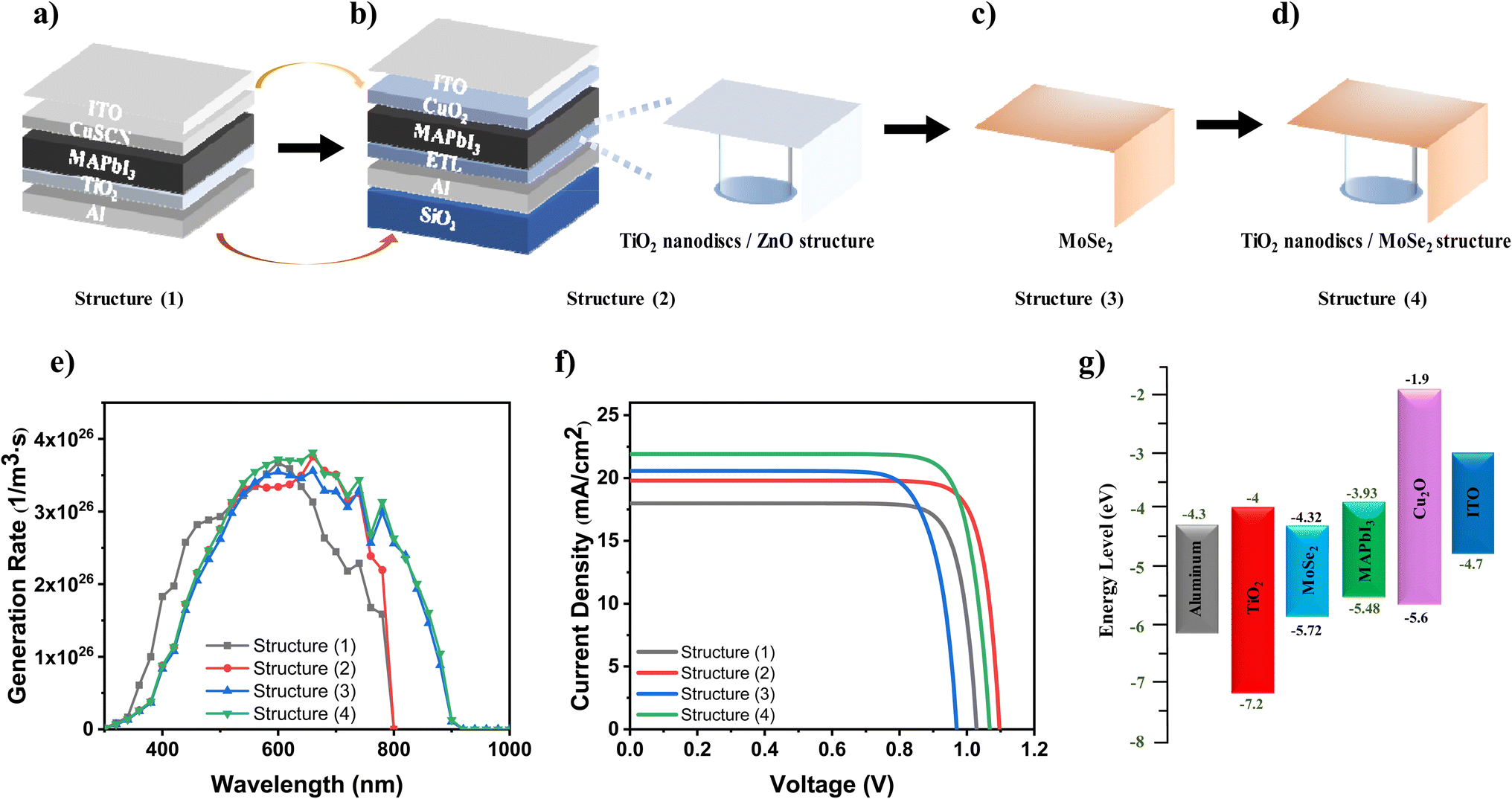
The planar reference structure, as shown in Fig. 7a, from top to bottom was composed of ITO as a transparent contact, CuSCN as the HTL, MAPbI3 as the active layer, TiO2 as the ETL, and Al as the metal contact. Finally, four main structures were investigated, which can be explained as: (1) the planar reference structure (Fig. 7a), (2) the proposed metasurface-based structure with ZnO around the TiO2 nanodiscs as ETL, and Cu2O as HTL (Fig. 7b), (3) the planar structure with MoSe2 as ETL and the second absorbent, and Cu2O as HTL (Fig. 7c), and (4) the metasurface-based structure with MoSe2 around TiO2 nanodiscs as the second absorbent, and Cu2O as HTL (Fig. 7d). The presence of TiO2 nanodiscs can improve the efficiency of the system in two ways: (1) creating a metasurface reflector to increase the light reflection from the lower surface of the active layer to increase the Jsc value, and (2) improving the electron transfer through the nanodiscs, which increases Voc. According to Fig. 7e, the carrier generation rate was higher in the structure (4) compared to the other structures owing to the presence of both the MoSe2 as the second absorbent layer and the TiO2 nanodiscs. The increase in the carrier generation rate, resulted in an increase in the Jsc value. According to Fig. 7f, which demonstrates the current density curves in terms of voltage, the Jsc value of the structure (4) is higher than the other structures due to the smaller bandgap of MoSe2 compared to MAPbI3, which absorbs light with wavelengths greater than 800 nm in the infrared region, as well as the higher light reflectance caused by the TiO2 nanodiscs. Utilizing the TiO2 nanodiscs along with ZnO in the structure (2) enhanced the carrier transfer rate, where both materials acted as hole blockers in the system. Therefore, the Voc value was increased slightly more than the other structures. On this account, structure (2) held a higher Voc value compared to structures (3 and 4) in light of the lack of proper hole blocking in MoSe2, which consequently increased the carrier recombination rate. Fig. 7g presents the energy band diagram related to the metasurface-based structure, where the TiO2 nanodiscs were surrounded by the MoSe2. In order to further discuss the lower Voc of the structures (3 and 4), the electrical properties of MoSe2 were studied. As indicated in Table 1, MoSe2 has an electron affinity equal to 4.32 eV and a bandgap equal to 1.4 eV. As a consequence of the lower energy level of the conduction band in MoSe2 compared to MAPbI3, the generated electrons in MAPbI3 layer were able to be transferred into the metal contact, which resulted in lower Voc values of the structures (3 and 4) compared to structure (2). However, the lower energy level of the valence band in MoSe2 compared to MAPbI3, was beneficial as it prevented the generated holes in MAPbI3 from entering the metal contact and transferring the generated holes in MoSe2 into the MAPbI3.
 |
| | Fig. 7 The device architecture for (a) the planar reference structure (structure (1)), (b) the proposed metasurface-based structure with ZnO around the TiO2 nanodiscs as ETL, and Cu2O as HTL (structure (2)), (c) the planar structure with MoSe2 as ETL and the second absorbent, and Cu2O as HTL (structure (3)), and (d) the metasurface-based structure with MoSe2 around TiO2 nanodiscs as the second absorbent, and Cu2O as HTL (structure (4)). The (e) carrier generation rate in terms of wavelength, and (f) current density in terms of voltage for the provided structures 1 to 4. (g) Band diagram of the structure 4 (all energy levels depicted in this diagram are based on the values listed in Table 1). | |
Table 5 displays the values of the Jsc, Voc, PCE, and FF for the structures (1 to 4). The Jsc value was enhanced from 19.80 mA cm−2 to 21.91 mA cm−2, when the MoSe2 was applied into the structure (2) instead of the ZnO. However, as a result of the better electron transfer and hole blocking in the ZnO layer compared to MoSe2, the value of the Voc in structure (3) fell from 1.09 V to 1.07 V compared to structure (2). Accordingly, the total PCE value was increased from 18.15% to 19.17%, when MoSe2 replaced the ZnO around the TiO2 nanodiscs. Both structures (2 and 4) were improved, comparing their electrical characteristics including Jsc, Voc, PCE, and FF to the planar structures (1 and 3) provided in Table 5, respectively. However, structure (4) was improved more significantly and reached the highest value of PCE equal to 19.17% as the champion structure among others. Also, the lack of optimal carrier separation in the system reduces the FF. By incorporating MoSe2 into the structure, due to its narrow band diagram, some electrons generated in the MAPbI3 layer enter the HTL. As illustrated in the band diagram of the structure (Fig. 7g), the electron entry into the HTL increases the series resistance, thereby reducing the FF. Additionally, some of these electrons recombine with the holes in the HTL, which leads to a decrease in the Voc when using MoSe2. However, considering the significant increase in Jsc compared to the decreases in Voc and FF, it can be concluded that MoSe2 is a better choice compared to ZnO.
Table 5 Comparison of the Jsc, Voc, PCE and FF values for different structures of: (1) the planar reference structure, (2) the proposed metasurface-based structure with ZnO around the TiO2 nanodiscs as ETL, and Cu2O as HTL, (3) the planar structure with MoSe2 as ETL and the second absorbent, and Cu2O as HTL, and (4) the metasurface-based structure with MoSe2 around TiO2 nanodiscs as the second absorbent, and Cu2O as HTL
| Structure |
J
sc (mA cm−2) |
V
oc (V) |
PCE (%) |
FF |
| 1 |
17.98 |
1.03 |
15.33 |
0.84 |
| 2 |
19.80 |
1.09 |
18.15 |
0.83 |
| 3 |
20.56 |
0.97 |
15.75 |
0.78 |
| 4 |
21.91 |
1.07 |
19.17 |
0.82 |
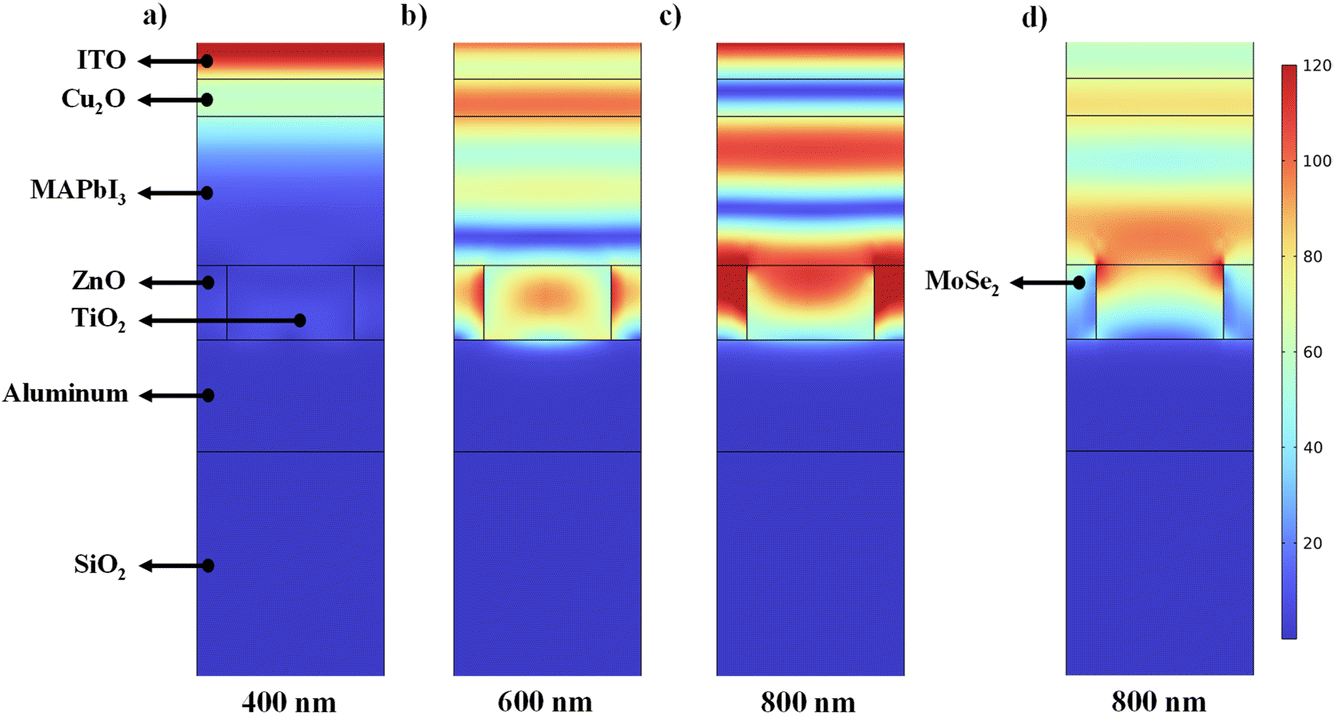
Fig. 8 illustrates the electric field distribution in three different wavelengths of 400, 600, and 800 nm for the structure (2) and at the wavelength of 800 nm for the structure (4). At the wavelength of 400 nm, provided in Fig. 8a, only a small percentage of the electric field entered the active layer due to light absorption in HTL (Cu2O), where it absorbed approximately 30% of the input power, which is less than other materials. At the wavelength of 600 nm, according to Fig. 8b, the layers above the active layer (ITO and Cu2O) showed no light absorption. In fact, Fig. S4(b) and S6(b)† indicate that most of the sunlight reached the active layer. About 75% of the incident light was absorbed in the active layer, together with the reflected light from the lower layers. Additionally, a strong electric field was formed around the TiO2 nanodiscs due to their resonances. At the wavelength of 800 nm, according to Fig. 8c, the electric field reached the ETL. Due to the light reflection from the metasurface reflector and the resonance of the electric field between the nanodiscs, a strong field was formed in the ETL as well as the lower part of the active layer. Applying MoSe2 as an absorbent material with the smaller bandgap than MAPbI3 intensified the transmitted electric field through the active layer and increased the PCE. Fig. 8d shows the electric field distribution at the wavelength of 800 nm for structure (4). Moreover, a significant portion of the electric field around the TiO2 nanodiscs that was depicted in Fig. 8c was absorbed by MoSe2 in structure (4). According to Fig. 7e, the overall light absorptance and carrier generation of structure (4) in the presence of MoSe2 at the wavelength of 800 nm seemed to have a significant portion, while for structure (2), this value is zero at this wavelength.
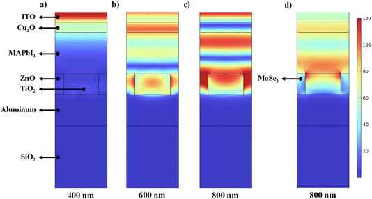 |
| | Fig. 8 Distribution of the electric field for the single junction metasurface reflector at different wavelengths of (a) 400 nm, (b) 600 nm, and (c) 800 nm. (d) Distribution of the electric field for the structure in the presence of MoSe2 as the second absorbent layer at the wavelength of 800 nm. | |
4. Conclusion
The efficiency of an inverted perovskite solar cell using a new perfect metasurface-based reflector with TiO2 nanodiscs/MoSe2 structure as ETL was enhanced through several optimizations. Initially, the perfect metasurface-based reflector structure (TiO2/Al/SiO2) was investigated and compared in different types of nanostructures, including: four different nanocubes and nanodiscs structures. It was explored that using TiO2 as nanodiscs compared to TiO2 as a bulk layer on an Al substrate increased the reflectance from 78.08% to 97.95%. Subsequently, the light absorption in the active layer and the carrier transfer through the structure were improved. Additionally, different materials were investigated as the ETLs around the TiO2 nanodiscs (ZnO, AZO, CeO2, and TiGO-5), while other materials as an HTL above the active layer (CuSCN, Spiro-OMeTAD, CuI, and Cu2O). The optimum structure consisting of ITO/Cu2O/MAPbI3/TiO2 nanodiscs and ZnO/Al/SiO2, obtained the values of the Jsc, Voc, PCE, and FF equal to 19.80 mA cm−2, 1.09 V, 18.15%, and 0.83, respectively. By applying MoSe2 around TiO2 nanodiscs with a smaller bandgap than the MAPbI3, as the second absorbent in the infrared region, the electrical characteristics of the cell were improved compared to the planar reference invert solar cell structure (ITO/CuSCN/MAPbI3/TiO2/Al), where the values of the Jsc, Voc, and PCE were increased from 17.98 mA cm−2 to 21.91 mA cm−2, 1.03 V to 1.07 V, and 15.33% to 19.17%, respectively.
Data availability
The data supporting this article have been included as part of the ESI.† Additional datasets generated and analyzed during the study, including optoelectronic simulations and characterization results, can be made available upon reasonable request by contacting the corresponding author.
Author contributions
Javad Maleki and Maryam Shahrostami: conceptualization, data curation, formal analysis, investigation, methodology, software, validation, visualization, writing – original draft, writing – review & editing. Siming Huang: investigation, validation, visualization, writing – review & editing. Mojtaba Abdi-Jalebi: conceptualization, data curation, formal analysis, funding acquisition, investigation, methodology, project administration, supervision, resources, validation, visualization, writing – review & editing.
Conflicts of interest
The authors declare no conflict of interest.
Acknowledgements
M. A.-J. acknowledges the Department for Energy Security and Net Zero (Project ID: NEXTCCUS), University College London's (UCL) Research, Innovation and Global Engagement, University of Sydney–University College London Partnership Collaboration Awards, Cornell-UCL Global Strategic Collaboration Awards and UCL-IITD Joint seed fund for their financial support. M. A.-J. acknowledges the ACT program (Accelerating CCS Technologies, Horizon 2020 Project No. 691712) for the financial support of the NEXTCCUS project (Project ID: 327327). M. A.-J. and S. H. acknowledge the UCL-IISc Seed Grant and UCL-Peking University Strategic Partner Fund for financial support. We wish to acknowledge the support of the Henry Royce Institute for Advanced Materials through the Industrial Collaboration Programme (RICP-R4-100061) and MATcelerateZero (MATZ0), funded from a grant provided by the Engineering and Physical Sciences Research Council EP/X527257/1.
References
- S. Kanwal, M. T. Mehran, M. Hassan, M. Anwar, S. R. Naqvi and A. H. Khoja, An integrated future approach for the energy security of Pakistan: Replacement of fossil fuels with syngas for better environment and socio-economic development, Renewable Sustainable Energy Rev., 2022, 156, 111978 CrossRef CAS.
-
F. A. Malla, S. A. Bandh, S. A. Wani, A. T. Hoang and N. A. Sofi, Biofuels: Potential Alternatives to Fossil Fuels, in Biofuels in Circular Economy, Springer, 2023, pp. 1–15 Search PubMed.
- Y. Huang, J. Lin, Y. Wang, J. Min, R. Wang, D. Jin and B. Wei, Forecast of fossil fuel demand based on low carbon emissions from the perspective of energy security, Chem. Technol. Fuels Oils, 2023, 58(6), 1075–1082 CrossRef CAS.
- M. K. H. Rabaia, M. A. Abdelkareem, E. T. Sayed, K. Elsaid, K.-J. Chae, T. Wilberforce and A. Olabi, Environmental impacts of solar energy systems: A review, Sci. Total Environ., 2021, 754, 141989 CrossRef CAS PubMed.
- S. E. Hosseini and M. A. Wahid, Hydrogen from solar energy, a clean energy carrier from a sustainable source of energy, Int. J. Energy Res., 2020, 44(6), 4110–4131 CrossRef.
- C. M. S. Kumar, S. Singh, M. K. Gupta, Y. M. Nimdeo, R. Raushan, A. V. Deorankar, T. M. A. Kumar, P. K. Rout, C. S. Chanotiya and V. D. Pakhale,
et al., Solar energy: A promising renewable source for meeting energy demand in Indian agriculture applications, Sustain. Energy Technol. Assessments, 2023, 55, 102905 CrossRef.
- Y. Park, B. Zhao and S. Fan, Reaching the ultimate efficiency of solar energy harvesting with a nonreciprocal multijunction solar cell, Nano Lett., 2021, 22(1), 448–452 CrossRef PubMed.
- Z. Wu, E. Bi, L. K. Ono, D. Li, O. M. Bakr, Y. Yan and Y. Qi, Passivation Strategies for Enhancing Device Performance of Perovskite Solar Cells, Nano Energy, 2023, 108731 CrossRef CAS.
- Y.-E. Lye, K.-Y. Chan and Z.-N. Ng, A Review on the Progress, Challenges, and Performances of Tin-Based Perovskite Solar Cells, Nanomaterials, 2023, 13(3), 585 CrossRef CAS PubMed.
- M. Haghighi, N. Ghazyani, S. Mahmoodpour, R. Keshtmand, A. Ghaffari, H. Luo, R. Mohammadpour, N. Taghavinia and M. Abdi-Jalebi, Low-Temperature Processing Methods for Tin Oxide as Electron Transporting Layer in Scalable Perovskite Solar Cells, Sol. RRL, 2023, 7(10), 2201080 CrossRef CAS.
- M. Abdi Jalebi, The Future of Halide Perovskite Solar Cells, Nanoscale Adv. Mater., 2024, 1(2), 87–94, DOI:10.22034/nsam.2024.04.02.
- D. Wang, M. Chen, X. Lei, Y. Wang, Y. Bao, X. Huang, P. Zhu, J. Zeng, X. Wang and S. Tsang,
et al., All-In-One Additive Enabled Efficient and Stable Narrow-Bandgap Perovskites for Monolithic All-Perovskite Tandem Solar Cells, Adv. Mater., 2024, 2411677 CrossRef CAS PubMed.
- Z.-E. Shi, T.-H. Cheng, C.-Y. Lung, C.-W. Lin, C.-L. Wang, B.-H. Jiang, Y.-S. Hsiao and C.-P. Chen, Achieving over 42% indoor efficiency in wide-bandgap perovskite solar cells through optimized interfacial passivation and carrier transport, Chem. Eng. J., 2024, 498, 155512 CrossRef CAS.
- B. H. Jiang, Z. J. Gao, C. Y. Lung, Z. E. Shi, H. Y. Du, Y. W. Su, H. S. Shih, K. M. Lee, H. H. Hung and C. K. Chan,
et al., Enhancing the Efficiency of Indoor Perovskite Solar Cells through Surface Defect Passivation with Coplanar Heteroacene Cored A–D–A-type Molecules, Adv. Funct. Mater., 2024, 34(19), 2312819 CrossRef CAS.
- M. A. Mahmud, J. Zheng, J. F. Chang, G. Wang, C. Liao, M. H. Rahman, W. B. Tarique, S. Tang, J. Bing and C. G. Bailey,
et al., Halogenated Polycyclic Aromatic Hydrocarbon for Hole Selective Layer/Perovskite Interface Modification and Passivation for Efficient Perovskite-Organic Tandem Solar Cells with Record Fill Factor, Adv. Energy Mater., 2024, 2400691 CrossRef CAS.
- S. Liu, Z. Sun, X. Lei, T. Miao, Q. Zhou, R. Chen, J. Wang, F. Ren, Y. Pan and Y. Cai,
et al., Stable Surface Contact with Tailored Alkylamine Pyridine Derivatives for High-Performance Inverted Perovskite Solar Cells, Adv. Mater., 2024, 2415100 Search PubMed.
- B. Gil, A. J. Yun, J. Lim, J. Cho, B. Kim, S. Ryu, J. Kim and B. Park, Design of SnO2 Electron Transport Layer in Perovskite Solar Cells to Achieve 2000 h Stability Under 1 Sun Illumination and 85 °C, Adv. Mater. Interfaces, 2023, 10(11), 2202148 CrossRef CAS.
- A. A. Said, J. Xie and Q. Zhang, Recent progress in organic electron transport materials in inverted perovskite solar cells, Small, 2019, 15(27), 1900854 CrossRef PubMed.
- M. Noman, M. Shahzaib, S. T. Jan, S. N. Shah and A. D. Khan, 26.48% efficient and stable FAPbI 3 perovskite solar cells employing SrCu 2 O 2 as hole transport layer, RSC Adv., 2023, 13(3), 1892–1905 RSC.
- Q. Lin, D. J. Kubicki, M. Omrani, F. Alam and M. Abdi-Jalebi, The race between complicated multiple cation/anion compositions and stabilization of FAPbI 3 for halide perovskite solar cells, J. Mater. Chem. C, 2023, 11(7), 2449–2468 RSC.
- G. Nan, X. Zhang, M. Abdi-Jalebi, Z. Andaji-Garmaroudi, S. D. Stranks, G. Lu and D. Beljonne, How methylammonium cations and chlorine dopants heal defects in lead iodide perovskites, Adv. Energy Mater., 2018, 8(13), 1702754 CrossRef.
- Q. Lin, S. P. Senanayak, N. Yaghoobi Nia, M. Alsari, S. Lilliu and M. Abdi-Jalebi, Impact of A-Site Cation Modification on Charge Transport Properties of Lead Halide Perovskite for Photovoltaics Applications, Energy Technol., 2023, 11(9), 2300358 CrossRef CAS.
- H. Li, C. Ding, D. Liu, S. Yajima, K. Takahashi, S. Hayase and Q. Shen, Efficient Charge Transfer in MAPbI3 QDs/TiO2 Heterojunctions for High-Performance Solar Cells, Nanomaterials, 2023, 13(7), 1292 CrossRef CAS PubMed.
- D. M. Niedzwiedzki, H. Zhou and P. Biswas, Exciton binding energy of MAPbI3 thin film elucidated via analysis and modeling of perovskite absorption and photoluminescence properties using various methodologies, J. Phys. Chem. C, 2022, 126(2), 1046–1054 CrossRef CAS.
- T. Ouslimane, L. Et-Taya, L. Elmaimouni and A. Benami, Impact of absorber layer thickness, defect density, and operating temperature on the performance of MAPbI3 solar cells based on ZnO electron transporting material, Heliyon, 2021, 7(3), e06379 CrossRef CAS PubMed.
- Z. Hu, C. Liu and G. Li, Disordered optical metasurfaces: from light manipulation to energy harvesting, Adv. Phys.:X, 2023, 8(1), 2234136 Search PubMed.
- A. S. Rana, M. Zubair, Y. Chen, Z. Wang, J. Deng, M. T. S. Chani, A. Danner, J. Teng and M. Q. Mehmood, Broadband solar absorption by chromium metasurface for highly efficient solar thermophotovoltaic systems, Renewable Sustainable Energy Rev., 2023, 171, 113005 CrossRef CAS.
- M. I. Hossain, N. Yumnam, W. Qarony, A. Salleo, V. Wagner, D. Knipp and Y. H. Tsang, Non-resonant metal-oxide metasurfaces for efficient perovskite solar cells, Sol. Energy, 2020, 198, 570–577 CrossRef CAS.
- S. S. Bukhari, J. Vardaxoglou and W. Whittow, A metasurfaces review: Definitions and applications, Appl. Sci., 2019, 9(13), 2727 CrossRef CAS.
- A. V. Prokhorov, P. D. Terekhov, M. Y. Gubin, A. V. Shesterikov, X. Ni, V. R. Tuz and A. B. Evlyukhin, Resonant light trapping via lattice-induced multipole coupling in symmetrical metasurfaces, ACS Photonics, 2022, 9(12), 3869–3875 CrossRef CAS.
- H. Lu, X. Guo, J. Zhang, X. Zhang, S. Li and C. Yang, Asymmetric metasurface structures for light absorption enhancement in thin film silicon solar cell, J. Opt., 2019, 21(4), 045901 CrossRef CAS.
- D. Katrodiya, C. Jani, V. Sorathiya and S. K. Patel, Metasurface based broadband solar absorber, Opt. Mater., 2019, 89, 34–41 CrossRef CAS.
- S. K. Patel, J. Parmar and V. Katkar, Metasurface-based solar absorber with absorption prediction using machine learning, Opt. Mater., 2022, 124, 112049 CrossRef CAS.
- R. Bilal, M. Baqir, P. Choudhury, M. Naveed, M. Ali and A. Rahim, Ultrathin broadband metasurface-based absorber comprised of tungsten nanowires, Results Phys., 2020, 19, 103471 CrossRef.
-
M. A. Shameli and L. Yousefi, Absorption Enhancement in Thin-Film Solar Cells using Integrated Photonic Topological Insulators, in 2021 29th Iranian Conference on Electrical Engineering (ICEE), IEEE, 2021, pp. 826–830 Search PubMed.
-
C. Cotirlan-Simioniuc and I.-R. Schiopu, Metasurface integrated in thin solar cells for index modulation, in Society of Photo-Optical Instrumentation Engineers (SPIE) Conference Series, 2023, vol. 12493, p. 1249321 Search PubMed.
- S. Charola, S. K. Patel, K. Dalsaniya, R. Jadeja, T. K. Nguyen and V. Dhasarathan, Numerical investigation of wideband L-shaped metasurface based solar absorber for visible and ultraviolet region, Phys. B, 2021, 601, 412503 CrossRef CAS.
- V. Sorathiya, S. Lavadiya, A. AlGhamdi, O. S. Faragallah, H. S. El-sayed, M. M. Eid and A. N. Z. Rashed, A comparative study of broadband solar absorbers with different gold metasurfaces and MgF 2 on tungsten substrates, J. Comput. Electron., 2021, 20, 1840–1850 CrossRef CAS.
- S. Charola, S. K. Patel, J. Parmar and R. Jadeja, Broadband and angle-insensitive metasurface solar absorber, Opt. Quantum Electron., 2022, 54(6), 348 CrossRef.
- S. K. Patel, S. Charola, J. Parmar, M. Ladumor, Q. M. Ngo and V. Dhasarathan, Broadband and efficient graphene solar absorber using periodical array of C-shaped metasurface, Opt. Quantum Electron., 2020, 52, 1–19 CrossRef.
- A. Prathan, J. Sanglao, T. Wang, C. Bhoomanee, P. Ruankham, A. Gardchareon and D. Wongratanaphisan, Controlled structure and growth mechanism behind hydrothermal growth of TiO2 nanorods, Sci. Rep., 2020, 10(1), 8065 CrossRef CAS PubMed.
- R. A. Saleh, O. N. Salman and M. O. Dawood, Physical investigations of titanium dioxide nanorods film prepared by hydrothermal technique, J. Appl. Sci. Nanotechnol., 2021, 1(3), 32–41 CrossRef.
- Q. Fan, P. Huo, D. Wang, Y. Liang, F. Yan and T. Xu, Visible light focusing flat lenses based on hybrid dielectric-metal metasurface reflector-arrays, Sci. Rep., 2017, 7(1), 45044 CrossRef CAS PubMed.
- M. A. Rahman, Enhancing the photovoltaic performance of Cd-free Cu2ZnSnS4 heterojunction solar cells using SnS HTL and TiO2 ETL, Sol. Energy, 2021, 215, 64–76 CrossRef.
- Q. Cao, Y. Li, H. Zhang, J. Yang, J. Han, T. Xu, S. Wang, Z. Wang, B. Gao and J. Zhao,
et al., Efficient and stable inverted perovskite solar cells with very high fill factors via incorporation of star-shaped polymer, Sci. Adv., 2021, 7(28), eabg0633 CrossRef CAS PubMed.
- H. Li, C. Zhang, C. Gong, D. Zhang, H. Zhang, Q. Zhuang, X. Yu, S. Gong, X. Chen and J. Yang,
et al., 2D/3D heterojunction engineering at the buried interface towards high-performance inverted methylammonium-free perovskite solar cells, Nat. Energy, 2023, 1–10 Search PubMed.
- F. Ma, Y. Zhao, J. Li, X. Zhang, H. Gu and J. You, Nickel oxide for inverted structure perovskite solar cells, J. Energy Chem., 2021, 52, 393–411 CrossRef CAS.
- A. Ghosh, A. A. Hassan, H. Alrafai and S. K. A. Abdelrahim, A comprehensive study on electron and hole transport layers for designing and optimizing the efficiency of MoSe2-Based solar cells using numerical simulation techniques, Heliyon, 2024, 10(16), e35061 CrossRef CAS PubMed.
- Z. Cui, H. Wang, Y. Shen, K. Qin, P. Yuan and E. Li, MoSe2 and WSSe heterojunction with exceptional power conversion efficiency and photogalvanic effect, Mater. Today Phys., 2024, 40, 101317 CrossRef CAS.
- X. Li, S. Aftab, H. Liu, D. Vikraman, S. Hussain, J. Kang and A. A. Al-Kahtani, Enhancing perovskite solar cells and X-ray photodetectors with hybrid MoSe2@ CNT composites: a path to improved efficiency and sensitivity, J. Power Sources, 2024, 624, 235588 CrossRef CAS.
- L. Qiu, G. Si, X. Bao, J. Liu, M. Guan, Y. Wu, X. Qi, G. Xing, Z. Dai and Q. Bao, Interfacial engineering of halide perovskites and two-dimensional materials, Chem. Soc. Rev., 2023, 52(1), 212–247 RSC.
- X. Chen, X. Chen, Y. Han, C. Su, M. Zeng, N. Hu, Y. Su, Z. Zhou, H. Wei and Z. Yang, Two-dimensional MoSe2 nanosheets via liquid-phase exfoliation for high-performance room temperature NO2 gas sensors, Nanotechnology, 2019, 30(44), 445503 CrossRef CAS PubMed.
- M. Zhang, Y. Lin, J. Li, X. Wei, Y. Peng, Z. Wang and Z. Jiang, Interfacial Electronic and Photovoltaic Performance of a Novel Lead-Free Z-Scheme CsSnBr3/MoSe2 Perovskite Heterostructure: A Theoretical and Experimental Study, Sol. RRL, 2023, 7(3), 2200784 CrossRef CAS.
- F. I. Za’abar, Y. Yusoff, H. Mohamed, S. F. Abdullah, A. W. Mahmood Zuhdi, N. Amin, P. Chelvanathan, M. S. Bahrudin, K. S. Rahman and N. A. Samsudin,
et al., A numerical investigation on the combined effects of MoSe2 interface layer and graded bandgap absorber in CIGS thin film solar cells, Coatings, 2021, 11(8), 930 CrossRef.
- Ø. Nordseth, R. Kumar, K. Bergum, L. Fara, C. Dumitru, D. Craciunescu, F. Dragan, I. Chilibon, E. Monakhov and S. E. Foss,
et al., Metal oxide thin-film heterojunctions for photovoltaic applications, Materials, 2018, 11(12), 2593 CrossRef PubMed.
- M. K. Hossain, M. H. K. Rubel, G. I. Toki, I. Alam, M. F. Rahman and H. Bencherif, Effect of various electron and hole transport layers on the performance of CsPbI3-based perovskite solar cells: A numerical investigation in DFT, SCAPS-1D, and wxAMPS frameworks, ACS Omega, 2022, 7(47), 43210–43230 CrossRef CAS PubMed.
- Y. Ma, P. Ou, Z. Wang, A. Zhu, L. Lu, Y. Zhang, W. Zeng, J. Song and J. Pan, Interface engineering in CeO2 (1 1 1) facets decorated with CdSe quantum dots for photocatalytic hydrogen evolution, J. Colloid Interface Sci., 2020, 579, 707–713 CrossRef CAS PubMed.
- H. Zhang, P. Xu, G. Du, Z. Chen, K. Oh, D. Pan and Z. Jiao, A facile one-step synthesis of TiO 2/graphene composites for photodegradation of methyl orange, Nano Res., 2011, 4, 274–283 CrossRef CAS.
- V. Stengl, D. Popelková and P. Vlácil, TiO2–graphene nanocomposite as high performace photocatalysts, J. Phys. Chem. C, 2011, 115(51), 25209–25218 CrossRef CAS.
- S. A. Kazmi, S. Hameed, A. S. Ahmed, M. Arshad and A. Azam, Electrical and optical properties of graphene-TiO2 nanocomposite and its applications in dye sensitized solar cells (DSSC), J. Alloys Compd., 2017, 691, 659–665 CrossRef CAS.
- M. Shanmugam, A. Alsalme, A. Alghamdi and R. Jayavel, In-situ microwave synthesis of graphene–TiO2 nanocomposites with enhanced photocatalytic properties for the degradation of organic pollutants, J. Photochem. Photobiol., B, 2016, 163, 216–223 CrossRef CAS PubMed.
- M. Gholipoor, N. Solhtalab and M. H. Mohammadi, High-performance parallel tandem MoTe2/perovskite solar cell based on reduced graphene oxide as hole transport layer, Sci. Rep., 2022, 12(1), 20455 CrossRef CAS PubMed.
- M. M. Khatun, A. Sunny and S. R. Al Ahmed, Numerical investigation on performance improvement of WS2 thin-film solar cell with copper iodide as hole transport layer, Sol. Energy, 2021, 224, 956–965 CrossRef CAS.
- Y. Raoui, H. Ez-Zahraouy, N. Tahiri, O. El Bounagui, S. Ahmad and S. Kazim, Performance analysis of MAPbI3 based perovskite solar cells employing diverse charge selective contacts: Simulation study, Sol. Energy, 2019, 193, 948–955 CrossRef CAS.
-
Y. Wang, Z. Xia, Y. Liu and H. Zhou, Simulation of perovskite solar cells with inorganic hole transporting materials, in 2015 IEEE 42nd Photovoltaic Specialist Conference (PVSC), IEEE, 2015, pp. 1–4 Search PubMed.
-
H. Suman and A. Kumar, Two-terminal tandem solar cells based on perovskite and transition metal dichalcogenides, arXiv, 2021, preprint, arXiv:2110.13780, DOI:10.48550/arXiv.2110.13780.
-
E. I. Ahamed, M. Matin and N. Amin, Modeling and simulation of highly efficient ultra-thin CIGS solar cell with MoSe2 tunnel, in 2017 4th International Conference on Advances in Electrical Engineering (ICAEE), IEEE, 2017, pp. 681–685 Search PubMed.
|
| This journal is © The Royal Society of Chemistry 2025 |
Click here to see how this site uses Cookies. View our privacy policy here. 
 Open Access Article
 This Open Access Article is licensed under a
  a,
Maryam
Shahrostami‡
a,
Maryam
Shahrostami‡