
 Open Access Article
 This Open Access Article is licensed under a
 Creative Commons Attribution 3.0 Unported Licence
Chloride-improved crystallization in sequentially vacuum-deposited perovskites for p–i–n perovskite solar cells†
Jin
Yan
 ab,
Jasmeen
Nespoli
b,
Reinder K.
Boekhoff
ab,
Haoxu
Wang
a,
Timo
Gort
b,
Martijn
Tijssen
a,
Bernardus
Zijlstra
a,
Arjan
Houtepen
b,
Tom J.
Savenije
b,
Olindo
Isabella
a and
Luana
Mazzarella
*a
ab,
Jasmeen
Nespoli
b,
Reinder K.
Boekhoff
ab,
Haoxu
Wang
a,
Timo
Gort
b,
Martijn
Tijssen
a,
Bernardus
Zijlstra
a,
Arjan
Houtepen
b,
Tom J.
Savenije
b,
Olindo
Isabella
a and
Luana
Mazzarella
*a
aPVMD Group, Delft University of Technology, Mekelweg 4, 2628 CD Delft, The Netherlands. E-mail: l.mazzarella@tudelft.nl
bDepartment of ChemE, Delft University of Technology, Van der Maasweg 9, 2629 HZ Delft, The Netherlands
First published on 14th April 2025
Abstract
Sequential thermal evaporation is an emerging technique for obtaining perovskite (PVK) photoactive materials for solar cell applications. Advantages include solvent-free processing, accurate stoichiometry control, and scalable processing. Nevertheless, the power conversion efficiency (PCE) of PVK solar cells (PSCs) fabricated by evaporation still lags behind that of solution-processed PSCs. Here, based on multi-cycle sequential thermal evaporation, we systematically investigate the effects of the post-deposition annealing temperature on the PVK properties in terms of surface morphology, opto-electronic properties, and device performance. We find that the average grain size increases to almost 1 μm and charge carrier mobilities exceed 50 cm2 V−1 s−1 when the annealing temperature is increased to 170 °C. We introduce a trace of PbCl2 to the multi-cycle sequential deposition to improve the absorber crystallinity at a lower annealing temperature of 150 °C, as evidenced by the XRD and PL analyses. The resulting PSC in a p–i–n structure yields a PCE of 18.5% with a cell area of 0.09 cm2. With the same deposition parameters, the cell area is scaled up to 0.36 cm2, achieving champion PCEs of 17.06%. This indicates the great potential of this technology for the commercialization of PSCs in the future.
1. Introduction
Thermal evaporation is a promising technique for the commercialization of perovskite (PVK) solar cells (PSCs) due to its numerous advantages, including controllable thickness, solvent-free processing, and compatibility with textured substrates.1–3 Since the first work reported in 2013,4 remarkable progress has been achieved in this field. To date, PSCs based on vapor-deposited PVK have achieved a record power conversion efficiency (PCE) of 26.4%.5 Additionally, fully evaporated PSCs have demonstrated a PCE above 20%.6 Despite these significant advancements, several challenges hinder progress toward the industrial application of vacuum-based PSCs, including the control of organic ammonium compounds7 and the complexity associated with multisource deposition processes involving more than two precursors.8 In contrast to co-evaporation, sequential thermal evaporation demonstrates compatibility with in-line fabrication,9 and it exhibits enhanced reproducibility due to the absence of cross-influence among the sources during deposition.10 However, constrained by limitations in precursor mixing and interdiffusion, it is crucial to optimize the thickness of each layer during sequential deposition. Conversely, an excessive number of layers in sequential deposition is time-consuming compared to the co-evaporation process. As a result, there are limited reports on multi-cycle sequential vacuum deposition processes.11–13Thermally deposited films typically exhibit lower charge carrier mobility, primarily constrained by grain size, and a shorter carrier lifetime due to defects introduced during film preparation.14,15 These defects lead to photovoltage losses, which detrimentally affect device efficiency and stability.16,17 In solution-based processing, the incorporation of lead-based dopants or salts into the precursor solution, such as lead chloride (PbCl2)18 and lead thiocyanate (Pb(SCN)2),19 has emerged as an effective strategy to suppress non-radiative recombination. In contrast to solution-based approaches, the use of lead-based salts in thermal evaporation technology has been rarely reported, largely due to the challenges associated with controlling the sublimation of Pb(SCN)2.20 Different from lead-based salts, PbCl2 has been extensively studied not only in solution-based methods21,22 but also in vacuum-based deposition techniques,23,24 where it plays a crucial role in modulating crystallization dynamics and enhancing the optoelectronic properties of PVK materials.
Specifically, mixed cation, mixed halide perovskites, CsxFA1−xPbI3−xBrx exhibit thermal stability,25 phase stability,26 and tunable bandgaps (Eg),27 which satisfy the requirements for use as top cells in PVK/c-Si tandem devices enabling current matching. For PVK/c-Si tandem devices, a p–i–n structure is preferable due to the low parasitic absorption of the hole transporting layer.28 To date, studies on sequential multi-cycle vacuum deposited CsxFA1−xPbI3−xBrx remain limited. Feng et al.29 demonstrated a sequential deposition method involving PbI2, FAI, and CsI, coupled with in vacuo annealing, achieving a champion efficiency of 21.3%. Similarly, Li et al.17 reported an efficiency exceeding 24% by first co-evaporation of PbI2, CsI, and PbCl2, followed by subsequent deposition of FAI. These studies highlight the high potential of sequential thermal evaporation technology for achieving elevated PCEs. However, both studies focus on the n–i–p structure and iodide-based PVK absorber, which are unsuitable as top cells when aiming for tandem device preparation.17,29
Based on the process proposed in our previous work,30,31 we demonstrate here efficient p–i–n PSCs based on multi-cycle thermally deposited CsxFA1−xPbI3−xBrx. In this work, the impact of post-deposition annealing is systematically investigated in terms of crystallinity, morphology, opto-electronic properties and performance. We find that the grain size increases on average from 500 nm to 1 μm as the annealing temperature increases from 130 °C to 170 °C. We demonstrate that a trace amount of PbCl2 improves the PCE by enhancing the open circuit voltage (Voc) and fill factor (FF), which is attributed to the improved absorber crystallinity. With these optimized parameters, we fabricate p–i–n solar cells with cell area of 0.09 cm2, achieving an efficiency of 18.5% with a Voc of 1.001 V, a short circuit-current (Jsc) of 23.75 mA cm−2, and a FF of 78.5%. These results show comparable device performance, especially the high FF, to co-evaporated MA-free based perovskites. Furthermore, the best PSCs achieve the highest PCE of 17.06% for 0.36 cm2. Our findings provide an alternative approach for thermal evaporated absorber preparation and scaling up in PSC applications.
2. Methodology
2.1 Materials
Indium tin oxide (ITO)-coated glass substrates and PTAA were purchased from Yokou. CsBr, fullerene (C60) and BCP were purchased from Sigma-Aldrich. CH(NH2)2I (FAI), PbCl2, and PbI2 were purchased from Greatcell Solar Materials. All chemicals are used as received.2.2 Film and device preparation
ITO-coated glass substrates were cleaned with acetone, ethanol, and oxygen plasma for 5–10 min. As a hole-extraction layer, 1.5 mg mL−1 PTAA was spin coated at 6000 rpm (acceleration 2000 rpm), and then annealed at 100 °C for 10 min. Then, the samples were transferred to a vacuum chamber (Perovap, CreaPhys) for PVK deposition at a base pressure of 10−6 mbar. PVK films are prepared with a simplified approach consisting of a multi-cycle sequential thermal deposition method described in our previous studies.30,31 To obtain a Cs0.15FA0.85PbI2.85Br0.15 film, three precursors were sequentially evaporated, PbI2, FAI, and CsBr, into one stack with a total thickness of 200–250 nm. Afterwards, two additional stacks were deposited by repeating the same sequence to reach a total target thickness of about 600 nm. A 1.8% molar ratio of PbCl2 to 1 of PbI2 was thermally deposited between the PbI2 and FAI layers in each stack for samples w/ PbCl2. Fig. 1a shows a schematic illustration of the sequential evaporation process. The detailed parameters for the deposition of each precursor are reported in Table S1.† The final PVK layers prepared in three cycles were annealed on a hot plate at different annealing temperatures (130 °C, 150 °C, and 170 °C) and times (10 min, 15 min, and 20 min). Afterwards, the samples were transferred into a second vacuum chamber (Optivap 2, CreaPhys) for the thermal evaporation of a 20 nm-thick C60 layer, and a 2 nm-thick BCP layer, followed by a 100-nm thick Ag electrode (Optivap 1, CreaPhys) using metal masks to define the cell area. | ||
| Fig. 1 (a) Schematic illustration of sequential thermal evaporation to prepare a PVK absorber. (b) XRD patterns of PVK films w/o and w/ PbCl2 subjected to different annealing temperatures for 10 minutes, and the XRD patterns are shifted for an easier comparison. Both the diffraction peak of PbI2 and PVK are illustrated with different symbols. (c) Cross-sectional SEM of PVKs at varying annealing temperatures (10 minutes) for both w/o and w/ PbCl2 samples. (d) FWHM and absolute peak intensities of the (100) crystal plane of w/o and w/ PbCl2 samples as a function of annealing temperature. (e) Grain size distribution of PVK films w/ PbCl2 at different annealing temperatures. Grain sizes were measured using ImageJ software and data were extracted from top view SEM images in Fig. S1.† | ||
2.3 Characterization
X-ray diffraction patterns (XRD) were measured with a Bruker D8 Advance diffractometer equipped with a Cu-Kα X-ray source at a wavelength of 1.54 Å.The top-view morphology and cross-section of PVK films and devices were measured using a scanning electron microscope (SEM, Thermo Scientific) with an accelerating voltage of 5 kV.
The absorption of samples was measured by ultraviolet-visible spectroscopy (UV/vis, PerkinElmer, Lambda 950) over a wavelength range of 300–850 nm.
The photoluminescence spectra of the samples were investigated by steady-state photoluminescence (PL, HORIBA, FL3-111) with an excitation wavelength of 405 nm; besides, the emission light was filtered using a 550 nm filter. Time-resolved photoluminescence spectra were recorded using an Edinburgh LifeSpec spectrometer equipped with a single-photon counter. The films were excited at 405 nm, and the emission light was filtered using a 550 nm filter.
Time-resolved microwave conductivity (TRMC) was applied to investigate the photo-induced carrier lifetime, mobility, and recombination dynamics (band-to-band recombination, trapping, and detrapping). The effective electron and hole mobilities (∑μ) are derived from the maximum TRMC signal (ΔGmax), which is normalized by the absorptance at an excitation wavelength of 650 nm. The charge carrier half-lifetime is obtained from the photoconductance decay.
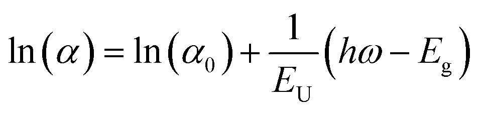
For the determination of the Urbach energy, sub-bandgap excitations from 750 nm to 950 nm (intervals of 25 nm) were performed. Thanks to the excellent sensitivity of TRMC, we calculated the absorption coefficient down to ∼10−2 cm−1 from the photoconductance and photo-induced carrier density upon sub-bandgap excitation, considering mobility, film thickness, photon fluence and reflection losses as previously reported.32 The Urbach energy, EU, is obtained by fitting the linear portion of the absorption coefficient (on a logarithmic scale) within the energy spectrum below the bandgap and calculating the inverse of the corresponding slope as shown in eqn (1).
 | (1) |
The current density–voltage (J–V) characteristics were recorded using a Keithley 2604 source-measure unit along with a solar simulator (OAI TriSol Class AAA) at 1 sun intensity, corrected by calculating the 1.2–1.28 sun shown on the run screen of the system. The J–V curve was obtained by scanning from 1.2 to −0.2 V and −0.2 to 1.2 V with a step size of 20 mV in both the forward and reverse sweeps. The active area of the solar cells was determined using the top metal contact, measuring 0.09 cm2 and 0.36 cm2.
3. Results and discussion
Based on the sequential thermal deposition approach described above, we investigated the impact of PbCl2 on the film properties at different annealing temperatures, including crystal structure, morphology, and optoelectronic properties. Samples without PbCl2 are denoted as w/o, while those with PbCl2 are referred to as w/ in the subsequent text and figures.Fig. 1b presents the X-ray diffraction (XRD) patterns of samples w/o and w/ PbCl2 annealed at temperatures ranging between 130 °C and 170 °C. The major peaks of the PVK films are located at 14.05° and 28.16°, which are assigned to the (100), and (200) crystal planes of cubic PVK, respectively. The absence of significant peak shifts across different conditions implies identical lattice constants (Table S2†) even with the introduction of trace amounts of PbCl2. However, the increasing peak intensities indicate improved crystallinity with higher annealing temperatures for both w/o and w/ PbCl2 samples. This observation is consistent with both top-view (Fig. S1†) and cross-sectional-view (Fig. 1c) SEM images. In Fig. 1c, the grain size shows a strong dependence on the annealing temperature. For both w/o and w/ PbCl2 samples, large grains form when the temperature exceeds 150 °C, whereas annealing conditions at lower temperature (≤150 °C) result in smaller grains throughout the film. To further investigate the effect of PbCl2, the full width at half maximum (FWHM) and the peak intensities of the w/o and w/ PbCl2 samples are reported in Fig. 1d as a function of annealing temperature. Interestingly, the w/ PbCl2 samples annealed at 130 °C show similar intensity and FWHM to the w/o PbCl2 samples annealed at 150 °C (highlighted in light orange and light blue bars in Fig. 1d), indicating improved crystallinity in the presence of PbCl2. Furthermore, both w/ PbCl2 samples annealed at 150 °C and 170 °C exhibit almost columnar grain growth, as shown in the cross-sectional SEM (Fig. 1c). This columnar growth has been reported to be beneficial for efficient charge carrier collection,33–35 as evidenced by the high FF in cell performance (Fig. S2†). In addition to the cross-sectional SEM, the grain size distribution statistics are summarized in Fig. 1e for samples w/ PbCl2 at different annealing temperatures. These data are extracted from the top-view SEM shown in Fig. S1.† Similar to the observations made in Fig. 1d, the grain size distribution confirms that in the presence of PbCl2, an annealing temperature of 150 °C is sufficient to convert the precursors into a dense PVK film with large grain sizes. Table S3† compares the grain size statistics obtained from top-view SEM with the crystallite size calculated using the Scherrer equation, both of which demonstrate improved crystallinity with increasing annealing temperature. This enhancement in crystal grains is consistent with previously published studies on both solution-processed and co-evaporated PSCs.24,36,37
Following the structural and morphological analysis, Fig. 2 shows the comparison of optoelectronic properties of w/o and w/ PbCl2 samples annealed at 150 °C. The UV-vis absorption spectra of the PVK films are shown in Fig. 2a. The higher absorption measured for the sample w/o PbCl2 compared to the w/ PbCl2 one can be related to small thickness variations. Fig. S3† shows the evolution of absorption with increasing annealing temperature for both w/o and w/ PbCl2 samples, together with a zoomed-in view of the absorption edge in the inset. Unlike the samples w/o PbCl2 shown in Fig. S3a,† the addition of PbCl2 in Fig. S3b† results in almost no change in the absorption edge for PVK films annealed at different temperatures. This difference indicates that PVK is fully converted already at a lower annealing temperature of 130 °C in the presence of PbCl2. Our conclusion is consistent with the XRD and SEM results discussed above. Fig. 2b displays the steady-state photoluminescent (PL) spectra of the two types of films. Compared to the w/o PbCl2 film, no significant shift in the peak position is observed in the PL spectrum of the PbCl2-based film. This aligns with the XRD peak positions provided in Table S2,† suggesting that Cl− is not incorporated into the PVK lattice but rather enhances the crystallization and conversion during annealing.36
 | ||
| Fig. 2 Opto-electronic properties of the w/o and w/ PbCl2 samples annealed at 150 °C for 10 minutes. (a) Absorptance spectra, (b) steady state PL, (c) TRPL decay, (d) PL intensity and half-lifetime as a function of annealing temperature; the comparison of PL intensity and half-lifetime is highlighted in light orange and light blue bars, (e) TRMC traces recorded under laser pulses at 650 nm, (f) Urbach energies for w/o and w/PbCl2 samples. | ||
To support the above conclusion, XPS spectra at different etching times are recorded to investigate the elemental composition of the PbCl2–PVK-based film, as shown in Fig. S4.† Interestingly, both the surface and bulk show no Cl signal. This could result from either a Cl content below the detection limit or from the fact that Cl evaporates in the form of an organic salt, as reported in ref. 36. However, the improved PL intensity with the introduction of PbCl2 indicates that the PbCl2-based film has fewer non-radiative recombination centres.38 Similarly, the TRPL decays are shown in Fig. 2c for both samples. The w/ PbCl2 PVK film shows a longer half-lifetime compared to the w/o PbCl2 film, indicating improved crystalline quality of the PbCl2-based films. To further verify the role of PbCl2, PL intensities and half-lifetimes are summarized in Fig. 2d as a function of annealing temperature (130 °C, 150 °C, and 170 °C) for both w/o and w/ PbCl2 samples. The samples w/ PbCl2 annealed at 130 °C show similar PL intensity and even a higher half lifetime (τ1/2) compared to the w/o PbCl2 sample annealed at 150 °C, highlighted in the light orange and light blue bars. This result indicates that introducing PbCl2 has similar effects to increasing the annealing temperature, both of which are related to enhanced film crystallinity and decreased trap states. Given that PbCl2 improves PVK crystallization as evidenced by XRD and PL, we applied time-resolved microwave conductivity (TRMC) to study the electronic properties and charge-carrier dynamics. An enhancement in the charge-carrier mobility by a factor of about 1.3 from 14.5 cm2 V−1 s−1 to 19.0 cm2 V−1 s−1 was observed, implying a significantly improved diffusion length for the w/ PbCl2 PVK (Fig. 2e). The increased mobility in the w/ PbCl2 sample can be attributed to the larger grains, as observed by SEM. Finally, the Urbach energies (EU), defining the sub-band gap tail states in the PVKs, were obtained by using TRMC for both samples.32Fig. 2f shows the logarithmic absorption coefficient, ln(α), as a function of the photon energy, Eph. From the resulting slope near the offset, the Urbach energy (EU) can be derived, amounting to 14.5 and 13.9 meV for the w/o PbCl2 and w/ PbCl2 PVK films, respectively (Fig. S5†). These relatively low EU values39 for both samples are indicative of a low degree of energetic disorder, implying a low concentration of sub gap tail states.
Next, we investigated the influence of annealing on the performance of solar cells, first w/o PbCl2 and later-on w/ PbCl2. The cell configuration is illustrated in Fig. S6.† Doubling the annealing time from 10 to 20 minutes at 150 °C shows a negligible impact on the photovoltaic parameters of the cell, as indicated in Fig. S7.† This result suggests that higher annealing temperatures are necessary to achieve improved PVK crystallization and enhanced cell efficiency, as evidenced by the high mobility (above 50 cm2 V−1 s−1) shown in Fig. S8.† However, PTAA is not thermally stable when the temperature is increased to 170 °C, even though this temperature is optimal for the absorber. The J–V curve of solar cells annealed at 170 °C in Fig. S8,† shows a significantly reduced PCE of below 10% compared to around 15% for the reference case annealed at 150 °C. Therefore, most of the discussion in the following part is limited to PVK annealed at 150 °C. The record solar cells with PbCl2-based PVK achieved a PCE of 18.5% in the forward bias scan (Voc = 1.001 V; Jsc = 23.75 mA cm2; FF = 78.5%), compared to 15.8% for the sample w/o PbCl2 (Voc = 0.85; Jsc = 23.88 mA cm2; FF = 76.3%). For a more exhaustive comparison, we report in Table S4† the solar cell parameters from the literature based on p–i–n cell structures. As evidenced by the film crystallinity and opto-electronic properties, the champion cell w/ PbCl2 shows improved Voc and FF compared to the sample w/o PbCl2 (Fig. 3a), benefitting from the enhanced passivation and the extended carrier diffusion length (lifetime and mobility). The PCE statistical distribution is summarized in Fig. 3b based on 20 solar cells for each condition, where the average PCEs are approximately 15.0% and 17.6% for the samples w/o and w/ PbCl2, respectively. The corresponding statistical distributions of the photovoltaic parameters (Voc, Jsc, and FF) are reported in Fig. S2.† Moreover, the statistics of the FF in reverse and forward scans are summarized in Fig. S9† for PSCs w/o and w/ PbCl2. In contrast to the samples w/o PbCl2, the PbCl2-based PSCs show comparable FF values for reverse and forward scans, demonstrating that PbCl2 effectively reduces the hysteresis, in agreement with findings for spin-coated PSCs.48,49 The reason of this improvement in hysteretic behavior could be attributed to fewer defect states near the surface of PVK/transporting layers.50 To further link the film morphology and optoelectronic properties to cell-level performance, we plotted the PCE and carrier mobility as a function of grain size in Fig. 3c, including data reported in the literature based on similar cell structures (p–i–n) and fabricated with thermally deposited absorbers. The data distribution clearly delineates two main regions, indicating that both PCE and carrier mobility are largely influenced by the grain size.
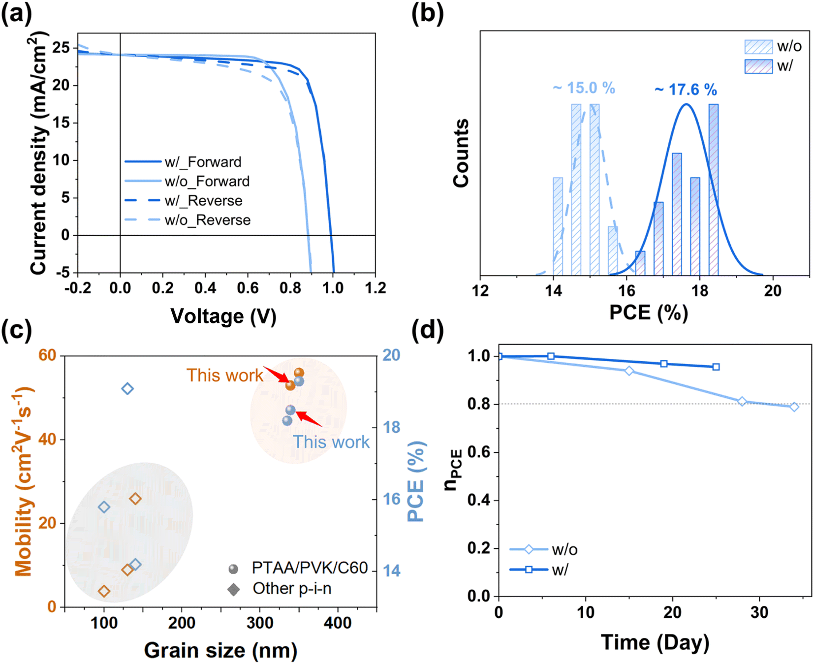 | ||
| Fig. 3 Photovoltaic performance of solar cells w/o and w/ PbCl2 annealed at 150 °C. (a) J–V curves in forward and reverse scan modes of the champion PSC and (b) PCE distribution of 20 cells for each condition, extracted from Fig. S2.† (c) Recently reported mobilities and PCEs as a function of grain size based on PSCs with thermally deposited absorbers. Sphere symbols represent the PTAA/PVK/C60 architecture,20 identical to the structure used in this study, while square symbols represent solar cells with other p–i–n.24,40–47 (d) Normalized PCE (nPCE) of p–i–n devices versus time over nearly 30 days with the solar cells are stored in a N2 filled glovebox between measurements. The solar cells area is 0.09 cm2. | ||
Benefiting from the reduced trap states, stability tests of the PSCs stored for 30 days in a glovebox proved that both PSCs w/o and w/ PbCl2, retained 77% and 88% of their initial efficiency, respectively (Fig. 3d). Besides, the sample with the introduction of PbCl2 also showed improved stability when the bare films were stored in ambient air compared to the reference sample; the corresponding photo is shown in Fig. S10.†
The PCE values of the PSCs reported above are all based on a cell area of 0.09 cm2; therefore we prepared devices with a cell area of 0.36 cm2 based on the absorber w/ PbCl2. Fig. 4a–c show dark and illuminated current density–voltage (J–V) curves in the forward and reverse scan directions of the champion PSCs with cell areas of 0.09 cm2 and 0.36 cm2, all annealed at 150 °C. The corresponding external parameters measured in the reverse/forward scans and the corresponding hysteresis values are reported in Table S5.† From the J–V curves, it is evident that the FF drops as cell area increases. Despite similar dark J–V characteristics, there is a marked difference in the slope of the light J–V curve at the 0 bias-voltage region, indicating significant photon-shunting as the cell areas increase. This is due to problems in carrier transport and interfacial accumulation. Interestingly, preliminary attempts to increase the cell area from 0.09 cm2 up to 1 cm2, show no Voc drop, as shown in Fig. S11,† which suggests the feasibility of preparing large-area cells without pinholes using this deposition technology. To further explore the impact of annealing temperature on cell performance as the cell area varies, we applied annealing temperatures of 130 °C, 150 °C, and 170 °C to the absorber for cells with areas of 0.09 cm2 and 0.36 cm2. The corresponding cell statistics are summarized in Fig. 4d–f. Similar to what has been reported in the literature, Fig. 4d demonstrates a decrease in PCE as the cell area increases. However, this drop mainly results from reductions in both Jsc and FF because of carrier transport issues, as discussed in Fig. 4a–c. Notably, when increasing the active area from 0.09 cm2 to 0.36 cm2, the Voc remains largely unaffected, especially at low annealing temperatures, which helps exclude the influence of PTAA degradation. The Voc for larger cell areas shows relative variations between 1% and 2% as compared to the 0.09 cm2 PSCs. These findings further confirm the reduced trap densities and high uniformity of the thermally evaporated PVK thin films over larger areas. Moreover, it indicates that PCE losses over large areas are primarily due to the increased electrode resistance.
 | ||
| Fig. 4 Influence of annealing temperature on J–V curves and external parameters of w/ PbCl2 PSCs. (a–c) Dark, forward, and reverse J–V curves of PSCs with active areas ranging from 0.09 to 0.36 cm2 annealed at 150 °C. (d–f) Distribution of external parameters (PCE, Voc, Jsc, and FF) of PSCs as a function of annealing temperature and cell area. Data of more than 20 cells are collected for each variation. The cells reported here are prepared in the same batch. | ||
To assess the uniformity of large-area PVKs deposited via sequential evaporation, a 15.6 × 15.6 cm2 film (Fig. 5a) was deposited on glass and evaluated in terms of homogeneity of thickness, PL, and device performance. The thickness mapping of the sample in Fig. 5b indicates that the PVK layer thickness varies by less than 15% between the center and edges, confirming the potential of this deposition technique for fabricating highly efficient large-area devices. Besides, the non-uniformity decreases to less than 9% when excluding the external edges, as shown by the yellow dash line in Fig. 5b. In Fig. 5c, the PL distribution reveals relatively comparable signal intensities, indicating uniform emission properties across the film. In addition to the full area test, specific samples were selected from different regions for both film-level and device-level measurements. Fig. 5d shows the selected positions of the large-area PVK film (1, 5, 7, 9, 11 and 15) for PL and XRD investigations. It was found that the peak intensities of the (100) plane from XRD and bandgap values extracted from PL in different regions are comparable, as shown in Fig. 5e. This result suggests uniform crystallization and composition throughout the large-area PVK films. Fig. 5f and S12† present the performance of 0.09 cm2 wide solar cells, demonstrating that all photovoltaic parameters exhibit less than 10% variation across different positions, confirming the uniformity and reliability of the fabricated large-area PVK devices.
 | ||
| Fig. 5 Uniformity test of the large area PVK film in terms of thickness, crystal structure, optoelectronic properties, and device performance. PVK films shown here are fabricated with PbCl2 and annealed at 150 °C for 10 min. (a) Photograph of the sequentially thermal deposited PVK film. The substrate size in the photograph is 15.6 × 15.6 cm2, (b) thickness mapping of the film shown in (a), (c) PL mapping of film shown in (a), and (d) photograph of PVK films at different positions for the measurement of crystal structure, optoelectronic properties, and device performance. (e) Absolute peak intensity for the (100) crystal plane and bandgap as a function of samples from different positions on the large area film as shown in (d). (f) Boxplot distribution of PCEs at 6 different locations, with each location having 20 cells with an area of 0.09 cm2, as shown in Fig. 4a. | ||
4. Conclusion
In conclusion, we fabricated and characterized Cs0.15FA0.85PbI2.85Br0.15 films and p–i–n devices using sequential thermal evaporation. We found that the grain size of PVK films increases significantly from less than 200 nm to almost 1 μm as the annealing temperature increases from 130 °C to 170 °C. The introduction of minor amounts of PbCl2 in the sequential evaporation improves the perovskite crystallinity as evidenced by XRD, SEM, TRMC and PL as well as device performance. We experimentally demonstrated that the introduction of PbCl2 in the PVK film reduces the optimal annealing temperature promoting crystallization already at 150 °C. This finding enables the use of a wider range of organic hole transport layers that might not withstand higher temperature processes. The champion efficiency in this work is observed in devices w/ PbCl2 and annealed at 150 °C, achieving a maximum power conversion efficiency of 18.5% and exhibiting a Voc and a FF of 1.001 V and 78.5%, respectively, for 0.09 cm2 wide cell. Building on these optimized parameters, we increased the device size up to 0.36 cm2. Despite the increase in cell area, larger area devices showcase a Voc >1 V. Besides, 15.6 × 15.6 cm2 perovskite films were prepared with uniform crystallization and comparable photovoltaic parameters, showing less than 10% variation across different positions. These results indicate the potential of this technology for the commercialization of perovskite solar cells.Data availability
The data supporting this article have been included as part of the ESI.†Conflicts of interest
There are no conflicts to declare.References
- Y. Vaynzof, Adv. Energy Mater., 2020, 10, 2003073 CrossRef CAS.
- J. Yan, T. J. Savenije, L. Mazzarella and O. Isabella, Sustainable Energy Fuels, 2022, 6, 243–266 RSC.
- S. R. Bae, D. Y. Heo and S. Y. Kim, Mater. Today Adv., 2022, 14, 100232 CrossRef CAS.
- M. Liu, M. B. Johnston and H. J. Snaith, Nature, 2013, 501, 395–398 CrossRef CAS.
- J. Zhou, L. Tan, Y. Liu, H. Li, X. Liu, M. Li, S. Wang, Y. Zhang, C. Jiang, R. Hua, W. Tress, S. Meloni and C. Yi, Joule, 2024, 8, 1691–1706 CrossRef CAS.
- C. Momblona, L. Gil-Escrig, E. Bandiello, E. M. Hutter, M. Sessolo, K. Lederer, J. Blochwitz-Nimoth and H. J. Bolink, Energy Environ. Sci., 2016, 9, 3456–3463 RSC.
- M. Kroll, S. D. Öz, Z. Zhang, R. Ji, T. Schramm, T. Antrack, Y. Vaynzof, S. Olthof and K. Leo, Sustainable Energy Fuels, 2022, 6, 3230–3239 RSC.
- L. Gil-Escrig, C. Dreessen, F. Palazon, Z. Hawash, E. Moons, S. Albrecht, M. Sessolo and H. J. Bolink, ACS Energy Lett., 2021, 6, 827–836 CrossRef CAS PubMed.
- M. Kam, Y. Zhu, D. Zhang, L. Gu, J. Chen and Z. Fan, Sol. RRL, 2019, 3, 1900050 CrossRef.
- J. H. Lee, B. S. Kim, J. Park, J. W. Lee and K. Kim, Adv. Mater. Technol., 2022, 8, 2200928 CrossRef.
- C. W. Chen, H. W. Kang, S. Y. Hsiao, P. F. Yang, K. M. Chiang and H. W. Lin, Adv. Mater., 2014, 26, 6647–6652 CrossRef CAS PubMed.
- Y. Zhang, L. Luo, J. Hua, C. Wang, F. Huang, J. Zhong, Y. Peng, Z. Ku and Y.-b. Cheng, Mater. Sci. Semicond. Process., 2019, 98, 39–43 CrossRef CAS.
- M. M. Tavakoli, A. Simchi, X. Mo and Z. Fan, Mater. Chem. Front., 2017, 1, 1520–1525 RSC.
- A. Babaei, W. Soltanpoor, M. A. Tesa-Serrate, S. Yerci, M. Sessolo and H. J. Bolink, Energy Technol., 2019, 8, 1900784 CrossRef.
- H. Li, M. Liu, M. Li, H. Park, N. Mathews, Y. Qi, X. Zhang, H. J. Bolink, K. Leo, M. Graetzel and C. Yi, iEnergy, 2022, 1, 434–452 Search PubMed.
- L. Gil-Escrig, C. Dreessen, I. C. Kaya, B.-S. Kim, F. Palazon, M. Sessolo and H. J. Bolink, ACS Energy Lett., 2020, 5, 3053–3061 CrossRef CAS.
- L. Hang, Z. Junjie, T. Liguo, L. Minghao, J. Chaofan, W. Siyang, Z. Xing, L. Yue, Z. Yu, Y. Yiran, T. Wolfgang and Y. Chenyi, Sci. Adv., 2022, 8, 8 CrossRef PubMed.
- W. Kaiser, E. Radicchi, E. Mosconi, A. Kachmar and F. De Angelis, ACS Appl. Energy Mater., 2021, 4, 9827–9835 CrossRef CAS.
- Y. Sun, J. Peng, Y. Chen, Y. Yao and Z. Liang, Sci. Rep., 2017, 7, 46193 CrossRef CAS PubMed.
- P. Y. Lin, A. Loganathan, I. Raifuku, M. H. Li, Y. Y. Chiu, S. T. Chang, A. Fakharuddin, C. F. Lin, T. F. Guo and L. Schmidt-Mende, Adv. Energy Mater., 2021, 11, 2100818 CrossRef CAS.
- X. Qi, G. Liu, D. Wang, N. Zhu, Y. Zhang, Z. Zhang, C. Wu, X. Li, W. Luo, Y. Li, H. Hu, Z. Chen, L. Xiao, S. Wang and B. Qu, Org. Electron., 2019, 74, 52–58 CrossRef CAS.
- S. Chen, X. Yu, X. Cai, M. Peng, K. Yan, B. Dong, H. Hu, B. Chen, X. Gao and D. Zou, RSC Adv., 2016, 6, 648–655 RSC.
- H. Li, L. Tan, C. Jiang, M. Li, J. Zhou, Y. Ye, Y. Liu and C. Yi, Adv. Funct. Mater., 2022, 33, 2211232 CrossRef.
- K. B. Lohmann, S. G. Motti, R. D. J. Oliver, A. J. Ramadan, H. C. Sansom, Q. Yuan, K. A. Elmestekawy, J. B. Patel, J. M. Ball, L. M. Herz, H. J. Snaith and M. B. Johnston, ACS Energy Lett., 2022, 7, 1903–1911 CrossRef CAS PubMed.
- L. Xie, P. Song, L. Shen, J. Lu, K. Liu, K. Lin, W. Feng, C. Tian and Z. Wei, J. Mater. Chem. A, 2020, 8, 7653–7658 RSC.
- R. Larciprete, A. Agresti, S. Pescetelli, H. Pazniak, A. Liedl, P. Lacovig, D. Lizzit, E. Tosi, S. Lizzit and A. Di Carlo, Materials, 2021, 14, 3954 CrossRef CAS PubMed.
- Y. Li, Y. Lu, X. Huo, D. Wei, J. Meng, J. Dong, B. Qiao, S. Zhao, Z. Xu and D. Song, RSC Adv., 2021, 11, 15688–15694 RSC.
- F. Fu, J. Li, T. C. Yang, H. Liang, A. Faes, Q. Jeangros, C. Ballif and Y. Hou, Adv. Mater., 2022, 34, e2106540 CrossRef PubMed.
- J. Feng, Y. Jiao, H. Wang, X. Zhu, Y. Sun, M. Du, Y. Cao, D. Yang and S. Liu, Energy Environ. Sci., 2021, 14, 3035–3043 RSC.
- J. Yan, J. Zhao, H. Wang, M. Kerklaan, L. J. Bannenberg, B. Ibrahim, T. J. Savenije, L. Mazzarella and O. Isabella, ACS Appl. Energy Mater., 2023, 6, 10265–10273 CrossRef CAS.
- J. Yan, L. S. Stickel, L. van den Hengel, H. Wang, P. R. Anusuyadevi, A. Kooijman, X. Liu, B. Ibrahim, A. Mol, P. Taheri, L. Mazzarella, O. Isabella and T. J. Savenije, J. Phys. Chem. Lett., 2023, 14, 8787–8795 CrossRef CAS PubMed.
- V. M. Caselli, Z. Wei, M. M. Ackermans, E. M. Hutter, B. Ehrler and T. J. Savenije, ACS Energy Lett., 2020, 5, 3821–3827 CrossRef CAS.
- J. X. Zhong, W. Q. Wu, J. F. Liao, W. Feng, Y. Jiang, L. Wang and D. B. Kuang, Adv. Energy Mater., 2020, 10, 1902256 CrossRef CAS.
- X. Cao, L. Zhi, Y. Li, F. Fang, X. Cui, L. Ci, K. Ding and J. Wei, ACS Appl. Energy Mater., 2018, 1, 868–875 CrossRef CAS.
- H. Eggers, F. Schackmar, T. Abzieher, Q. Sun, U. Lemmer, Y. Vaynzof, B. S. Richards, G. Hernandez-Sosa and U. W. Paetzold, Adv. Energy Mater., 2019, 10, 1903184 CrossRef.
- K. H. Stone, A. Gold-Parker, V. L. Pool, E. L. Unger, A. R. Bowring, M. D. McGehee, M. F. Toney and C. J. Tassone, Nat. Commun., 2018, 9, 3458 CrossRef PubMed.
- X. Wang, J. Fang, S. Li, G. Xie, D. Lin, H. Li, D. Wang, N. Huang, H. Peng and L. Qiu, Small, 2024, 20, e2404058 CrossRef PubMed.
- Y. Shao, Z. Xiao, C. Bi, Y. Yuan and J. Huang, Nat. Commun., 2014, 5, 5784 CrossRef CAS PubMed.
- B. Subedi, C. Li, C. Chen, D. Liu, M. M. Junda, Z. Song, Y. Yan and N. J. Podraza, ACS Appl. Mater. Interfaces, 2022, 14, 7796–7804 CrossRef CAS PubMed.
- M. Piot, J. E. S. Alonso, K. P. S. Zanoni, N. Rodkey, F. Ventosinos, C. Roldan-Carmona, M. Sessolo and H. Bolink, ACS Energy Lett., 2023, 8, 4711–4713 CrossRef CAS PubMed.
- M. Ross, L. Gil-Escrig, A. Al-Ashouri, P. Tockhorn, M. Jost, B. Rech and S. Albrecht, ACS Appl. Mater. Interfaces, 2020, 12, 39261–39272 CrossRef CAS PubMed.
- J. Li, H. A. Dewi, H. Wang, J. Zhao, N. Tiwari, N. Yantara, T. Malinauskas, V. Getautis, T. J. Savenije, N. Mathews, S. Mhaisalkar and A. Bruno, Adv. Funct. Mater., 2021, 31, 2103252 CrossRef CAS.
- B. S. Kim, L. Gil-Escrig, M. Sessolo and H. J. Bolink, J. Phys. Chem. Lett., 2020, 11, 6852–6859 CrossRef CAS PubMed.
- A. Babaei, K. P. S. Zanoni, L. Gil-Escrig, D. Perez-Del-Rey, P. P. Boix, M. Sessolo and H. J. Bolink, Front. Chem., 2019, 7, 936 CrossRef CAS PubMed.
- T. Abzieher, T. Feeney, F. Schackmar, Y. J. Donie, I. M. Hossain, J. A. Schwenzer, T. Hellmann, T. Mayer, M. Powalla and U. W. Paetzold, Adv. Funct. Mater., 2021, 31, 2104482 CrossRef CAS.
- Y. H. Chiang, M. Anaya and S. D. Stranks, ACS Energy Lett., 2020, 5, 2498–2504 CrossRef CAS PubMed.
- R. Ji, Z. Zhang, C. Cho, Q. An, F. Paulus, M. Kroll, M. Löffler, F. Nehm, B. Rellinghaus, K. Leo and Y. Vaynzof, J. Mater. Chem. C, 2020, 8, 7725–7733 RSC.
- L. Li, P. Zhou, J. Li, Y. Mo, W. Huang, J. Xiao, W. Li, Z. Ku, J. Zhong, Y. Peng, Y.-B. Cheng and F. Huang, J. Mater. Chem. C, 2018, 6, 13157–13161 RSC.
- L. Fan, Y. Ding, J. Luo, B. Shi, X. Yao, C. Wei, D. Zhang, G. Wang, Y. Sheng, Y. Chen, A. Hagfeldt, Y. Zhao and X. Zhang, J. Mater. Chem. A, 2017, 5, 7423–7432 RSC.
- R. van Heerden, P. Procel, L. Mazzarella, R. Santbergen and O. Isabella, Front. Photonics, 2022, 3, 889837 CrossRef.
Footnote |
| † Electronic supplementary information (ESI) available. See DOI: https://doi.org/10.1039/d4se01744g |
| This journal is © The Royal Society of Chemistry 2025 |