
 Open Access Article
 This Open Access Article is licensed under a Creative Commons Attribution-Non Commercial 3.0 Unported Licence
Evolving solar cell manufacturing: the promising outlook of open-air perovskite printing
Naresh-Kumar Pendyala
 *a,
Ankita Kolay
b,
Yallam Naidu Ponnada
c,
Antonio Guerrero
a and
Lioz Etgar
d
*a,
Ankita Kolay
b,
Yallam Naidu Ponnada
c,
Antonio Guerrero
a and
Lioz Etgar
d
aInstitute of Advanced Materials (INAM), Universitat Jaume I, 12006 Castelló, Spain. E-mail: pendyala@uji.es
bDepartment of Chemical Sciences, Indian Institute of Science Education and Research (IISER) Kolkata, Mohanpur 741246, India
cDepartment of Chemistry, Indian Institute of Technology Hyderabad, Kandi, 502284, Sangareddy, Telangana, India
dInstitute of Chemistry, Casali Center for Applied Chemistry, The Hebrew University of Jerusalem, Jerusalem 91904, Israel
First published on 19th February 2025
Abstract
Perovskite-based solar cells stand out as promising candidates due to their remarkable optoelectronic properties and cost-effective processing methods. These advanced materials have garnered considerable research interest owing to their rapidly increasing power conversion efficiencies. Additionally, perovskite solar cells (PSCs) can be flexible, lightweight, and semi-transparent, expanding their applicability. While conventional spin-coating techniques have achieved record power conversion efficiencies for PSCs, scalability remains a challenge. Furthermore, these materials face two significant hurdles: instability when exposed to open air and concerns regarding chemical toxicity, primarily from lead (Pb) and solvent use. Recent advancements have focused on open-air printing techniques, which offer scalability and adaptability for large-scale production. However, the lack of standardized fabrication protocols and the need to mitigate chemical toxicity remain ongoing challenges. In this comprehensive review, we thoroughly examine the latest developments in perovskite solar cell technology, with a particular emphasis on open-air printing processes. We explore the strategies employed to enhance stability, efficiency, and scalability, highlighting the critical role of open-air printing in achieving these objectives. Furthermore, this review addresses the challenges and opportunities associated with open-air printing, including material synthesis, and device architecture. We analyze recent breakthroughs in materials and interface, and solvent engineering, as well as device fabrication techniques, driving advancements in the field towards simplified, large-area fabrication protocols for PSCs.
 Naresh-Kumar Pendyala | Dr Pendyala Naresh Kumar received his Master's degree in Chemistry from Kakatiya University, India, in 2011. In 2017, he earned his PhD in Chemistry from the Indian Institute of Technology Hyderabad (IIT-Hyderabad) for his research on inorganic quantum dot solar cells. Following his doctoral studies, Dr Naresh pursued postdoctoral research in China (2018–2019), where he worked on thin-film transistors. He then continued his research in Israel (2020–2022), focusing on semi-transparent perovskite solar cells utilizing inkjet printing technology. Since 2023, Dr Naresh has been working at Universitat Jaume I, Spain, where his research is centered on halide perovskite memory devices. His contribution, conceptual development, manuscript drafting, and overall organization. |
 Ankita Kolay | Dr Ankita Kolay received both her Master's degree in Chemistry in 2016 and PhD degree in 2021 from the Indian Institute of Technology (IIT) Hyderabad. Her doctoral research was focused on developing quantum dot solar cells integrated with electrochromic layers. Currently, she is pursuing post-doctoral research at the Indian Institute of Science Education and Research (IISER) Kolkata on the design of halide perovskite nanostructures and fabrication of perovskite optoelectronic devices. She contributed in drafting, preparing the figures and reorganization of the manuscript. |
 Yallam Naidu Ponnada | Ponnada Yallam Naidu received his Master's degree in Chemistry from Osmania University, India, in 2018. Since 2021, he is a PhD scholar at the Indian Institute of Technology (IIT) Hyderabad. His research is focused on designing liquid junction solar cell assemblies using metal chalcogenides and chromic metal oxide composites. He contributed in collection of the literature and preparing the table for the manuscript. |
 Antonio Guerrero | Prof. Antonio Guerrero, a chemist (2002, Alcalá de Henares, Spain), is an Associate Professor in Applied Physics at the University Jaume I. He obtained his PhD in Organometallic Chemistry (2006, University of East Anglia, UK) with industrial support from Bayer, focusing on catalyst design for plastic production. He then spent four years at Cambridge Display Technology developing advanced semiconducting materials for OLEDs. Since 2010, at the University Jaume I, his research has primarily focused on three areas: (1) photovoltaic applications, (2) electronic memory devices, and (3) advanced solutions for energy vectors and the Circular Economy. His contribution includes revising the MS. |
 Lioz Etgar | Prof. Lioz Etgar earned his PhD in 2009 from the Technion–Israel Institute of Technology and conducted postdoctoral research with Prof. Michael Grätzel at EPFL, Switzerland, receiving the Marie Curie Fellowship and Wolf Prize for Young Scientists. He joined the Hebrew University of Jerusalem in 2012, becoming a Full Professor in 2021. Prof. Etgar pioneered the use of perovskite as both a light harvester and hole conductor in solar cells, leading to a seminal publication in the field. Awarded the Krill Prize and Kaye Innovation Award, his research focuses on advanced solar cell and LED technologies. His contribution includes revising the MS. |
1. Introduction
Renewable and clean energy findings have become increasingly important in recent years as a means to combat climate change. The use of photovoltaic devices (solar cells) is a promising technology, which convert the freely available solar energy to electricity. According to current statistics, solar cells account for just 3.6% of global electricity production.1 However, current solar cells face several limitations, including high production costs, limited power conversion efficiency, heavy-weight modules, and a lack of tunable transparency, making them opaque and less versatile.2–4 To tackle these issues, researchers have focused on exploring halide perovskites for solar cells. However, fabrication of PSCs in open-air has remained challenging.5–7 Open-air fabrication is a process where materials are applied to a substrate within no sealed environment. This allows for more flexibility and lower costs to produce large-area solar cells.Perovskite materials have a distinctive crystal structure characterized by the chemical formula ABX3, where ‘A’ represents a monovalent cation, ‘B’ a divalent cation, and ‘X’ a monovalent anion. In perovskite-based solar cells (PSCs), the monovalent ‘A’ cations are typically alkyl amines or inorganic cations such as Cs+ and Rb+. The divalent ‘B’ positions within the lattice are occupied by metal ions like Pb, Sn, Cu, or Mn. The anionic components (‘X’) in the perovskite lattice are halides, such as I−, Br−, and Cl−, or a combination of these halides in mixed compositions. The mixed halide composition in perovskites can significantly influence their optical properties. Numerous research groups have explored mixed halide compositions in PSCs to achieve an optimal optical bandgap, enhancing both efficiency and transparency in solar cells. At the same time, several studies have focused on improving the stability of these solar cells by tuning the cationic composition.8–10
Semiconductors in solar cells with a bandgap of 1.1 to 3.5 eV are capable of absorbing solar radiation within the 1100–350 nm range. Identifying a semiconductor with both a high absorption coefficient and excellent charge mobility remains a critical challenge for achieving efficient solar cells. Notably, laboratory-scale PSCs have surpassed the efficiency of commercial multi-crystalline silicon solar cells and are now nearly on par with the performance of CIGS and CdTe thin-film solar cells.11,12 Similar to the PSCs, the colored organic dye and inorganic quantum dot solar cells have distinctive optical and structural properties and can be solution-processed. Nevertheless, their lower power conversion efficiencies (PCEs) have impeded their adoption in the photovoltaics field.13–26 Even though, the reached efficiencies for PSCs are high (Record PCE >26%,27), and set a benchmark, their long-term stability, chemical toxicity and scalability needs to be improved for commercial viability. Moreover, PSCs must withstand towards environmental factors like high temperatures, humidity, and UV-light over long duration of time. The morphology of perovskite solar cells has a significant impact on the efficiency and stability of the device. The morphology of perovskite is highly dependent on the fabrication process and has a significant effect on the performance of the device. This can be achieved by controlling the perovskite growth parameters such as temperature, pressure, and deposition rate. For perovskite solar cells, other than perovskite layer's quality, the electron transport layer (ETL), and hole transport layer (HTL) also play an important role. These layers provide a pathway for the electrons and holes to move from the perovskite layer to the electrodes. In recent times, the concept of structural confinement of perovskites has been introduced. The regular perovskite films are considered as bulk perovskite or 3D perovskites whereas if the A cite cation in ABX3 is larger than the BX6 octahedra, it forms sheets of corner shared 2D perovskite layers. Thus, the A cations used are alkyl/aryl amines with longer carbon chains that protect from moisture, improving the stability of the perovskite solar cell. Additionally, the confinement of the perovskite structure in lower dimensions allows for tuning of its optical properties.28–34 Thus, in this review, we have discussed the literature involved in perovskite's structural and compositional tuning, additive engineering, solvent engineering, surface treatments and process engineering, etc., in improving the open-air fabrication methodology.
2. Perovskite solar cell structure
The potential PSC device architectures are illustrated in Fig. 1(a–c), showcasing various construction approaches. These designs highlight different configurations and structural components crucial to optimizing the performance and efficiency of perovskite solar cells. Printed perovskite solar cells typically consist of multiple layers, including a transparent conductive electrode (such as indium tin oxide, ITO), a perovskite absorber layer, hole transport layer (HTL), electron transport layer (ETL), and metal contacts. Based on the solar cell construction, top layer's stability, fabrication temperatures, and device performance, one can choose to work with either n-i-p or p-i-n structures. The ETL, Perovskite, and HTL layers are deposited in a sequence over the conducting substrate to produce n-i-p structure and vice versa.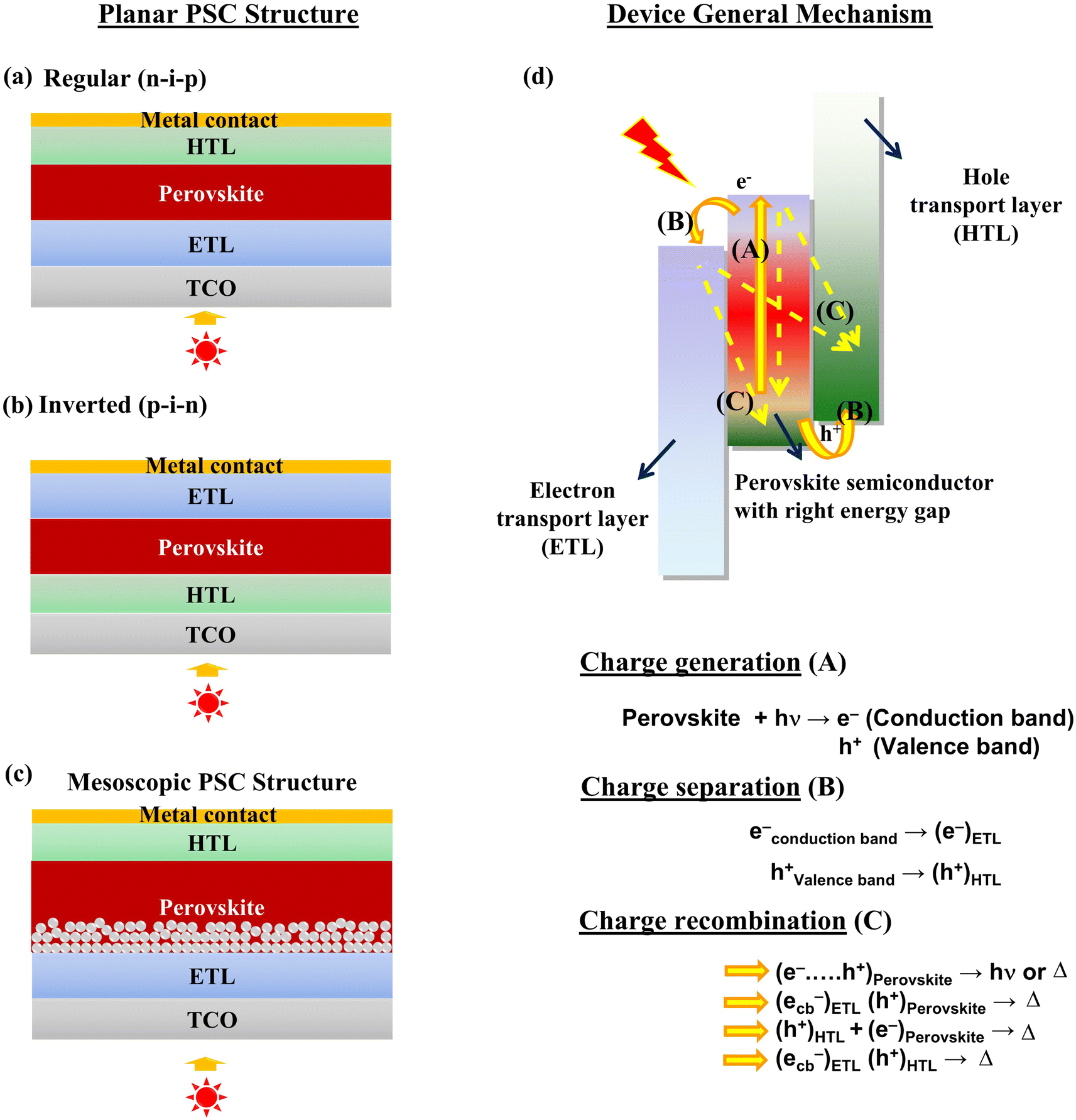 | ||
| Fig. 1 The schematic illustration details the sandwich structure of a perovskite solar cell in two configurations: n-i-p and p-i-n (a and b). It further illustrates the n-i-p configuration with a mesoporous structure (c), and demonstrates the process of charge generation under light, highlighting potential charge recombination pathways, including radiative (hν) and thermal (Δ) recombinations (d). | ||
Upon absorption of a photon from the solar radiation, the electron will be excited from the valence band to its conduction band (CB), leaving holes in the valence band (VB), as it is represented in Fig. 1b. Since the perovskite layer is sandwiched in between the ETL and the HTL. The photoelectron is transported to the load by the ETL, and the hole will be scavenged by the HTL. This directional movement of charges is driven by the built-in potential and the electric field within the device. Thus, the perovskite layer can produce electricity continuously out from the device until we stop irradiating the PSC. Under irradiation, three key processes occur in PSCs. The first is charge generation, where the perovskite layer acts as the primary light-absorbing material. The second is charge separation, facilitated by the interfaces between the perovskite, HTL, and ETL, which are crucial for efficient charge extraction. Finally, charge recombination can occur, often due to the presence of pinholes, cracks, or poor interfacial properties, which lead to the loss of charge carriers and diminished device performance.
The potential charge trapping defects and other challenges faced by perovskite materials are illustrated schematically in Fig. 2a–f. This figure highlights the key issues affecting perovskite performance, providing a visual representation of the various defects and obstacles that impact charge transport and overall efficiency. Compared to the lab-scale spin-coating method, open-air printing techniques encounter significant challenges in growing perovskite films. In open-air conditions, there is no control over oxygen and moisture exposure. If the perovskite formulation is not optimized, this can result in uncontrolled and non-uniform perovskite crystallization, leading to grain boundaries and surface dangling bonds. These imperfections are particularly vulnerable to air and moisture, resulting in poor interfaces and reduced charge separation efficiency. Additionally, the thickness of the perovskite film in large-scale production tends to be irregular, in contrast to the more consistent layers produced in lab-scale settings. This irregularity can cause photoelectrons to become trapped at defect sites, hindering their transport to charge collectors. Moreover, the lack of control over surface roughness in large-scale production further exacerbates the problem, increasing the series resistance (RS) and hampering efficient charge separation. Controlling perovskite thickness remains a significant challenge. The formation of cracks and pinholes during large-scale production further degrades performance, as these defects reduce shunt resistance (RSH), promote radiative charge recombination, and ultimately lead to poor PCE. Moreover, PSCs exhibit hysteresis in current–voltage measurements, primarily attributed to ion migration. Under applied voltage, halide ions and organic cations tend to migrate, causing chemical reactions at interfaces, penetration into electrode materials, and the formation of ionic double layers (Fig. 2g). These processes contribute to reduced device efficiency and stability. Additionally, the phase purity and uniformity of the perovskite material are strongly influenced by crystallization time (Fig. 2h). In open-air conditions, delayed crystallization often leads to suboptimal perovskite growth, significantly impairing both the overall efficiency and the long-term stability of PSCs.
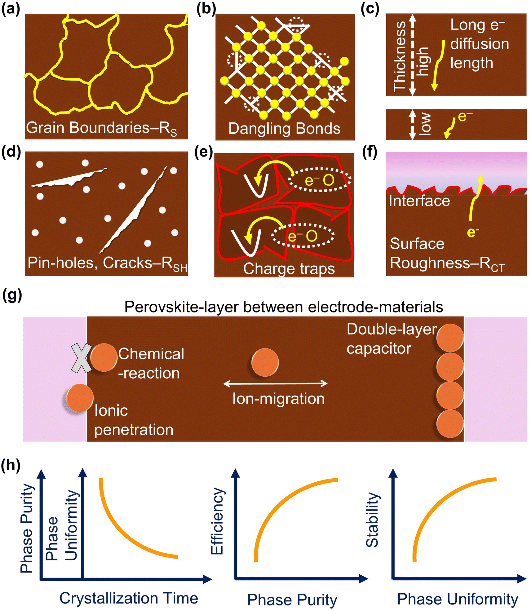 | ||
| Fig. 2 Key performance-influencing factors are identified, such as grain boundaries (a), dangling bonds on the perovskite surface (b), excessive thickness causing charge trapping (c), cracks and pinholes (d), and charge traps from all these lattice defects (e), surface roughness (f). Illustration of possible chemical reactivity, ion diffusion, double-layer capacitor formation, and ionic penetration within the perovskite layer under applied bias conditions (g). Additionally, the schematic explores the relationship between perovskite phase purity and perovskite crystallization time, the correlation between PSC efficiency and phase purity, and the impact of phase uniformity on device stability (h). | ||
To address this issue, researchers have employed various strategies such as encapsulation with moisture-resistant materials, interface engineering to minimize moisture ingress, and developing moisture-resistant perovskite compositions.
The degradation mechanisms of halide perovskites in open air typically involve the reaction of the halide ions (e.g., iodide, bromide, or chloride) with moisture and oxygen. One of the key reactions is the oxidation of the halide ions by oxygen, leading to the formation of halogen gases (e.g., iodine, bromine, or chlorine) and other byproducts. For example, in the case of methylammonium lead iodide perovskite, results in the formation of lead iodide (PbI2), methylamine (CH3NH2), molecular iodine (I2), and water (H2O), leading to the degradation of the perovskite structure and a decrease in device performance. Halide perovskites are also prone to thermal degradation, especially at elevated temperatures encountered during device fabrication processes or under operational conditions.35,36
Regardless of the perovskite deposition method, a critical step in device fabrication involves precisely controlling the perovskite layer's thickness, morphology, and crystallinity during the crucial phase transition from solution to solid film, as illustrated in the schematic (Fig. 3). The most commonly used solvents in the spin-coating approach are N,N-dimethylformamide (DMF) and dimethyl sulfoxide (DMSO). However, these solvents are less frequently used in large-scale printing techniques. For instance, Mai and his team used N-methyl-2-pyrrolidinone (NMP) that forms a stronger coordination with PbI2 compared to DMF or DMSO. This characteristic plays a crucial role in achieving uniform crystalline perovskite thin films through the blade-coating approach.37 However, aprotic solvents are not suitable for all perovskite formulations. For example, 1-methoxy-2-propanol (PM) has proven to be an effective co-solvent in the inkjet printing of uniform perovskite thin films.38 Similarly, in the blade-coating approach, 2-methoxyethanol is identified as an efficient solvent.39 This underscores the importance of carefully selecting appropriate solvents for perovskite processing. The illustration below demonstrates how lead halide coordinates with solvent molecules and alkylamines in the precursor solution state. This coordination also persists in the adduct state, where the thin film is initially deposited. However, the adduct form remains stable for only a few seconds, as the solvent molecules rapidly evaporate. To achieve better and more uniform crystallization, techniques such as antisolvent treatment or air-knife-assisted perovskite crystallization are employed. These methods facilitate the removal of solvent molecules, promoting the formation of crystalline films. In particular, the interaction between the antisolvent or the compressed air pressure, as well as the air-knife's duration over the film, plays a crucial role in ensuring the complete extraction of residual solvent molecules from the evolving perovskite lattice.40–42
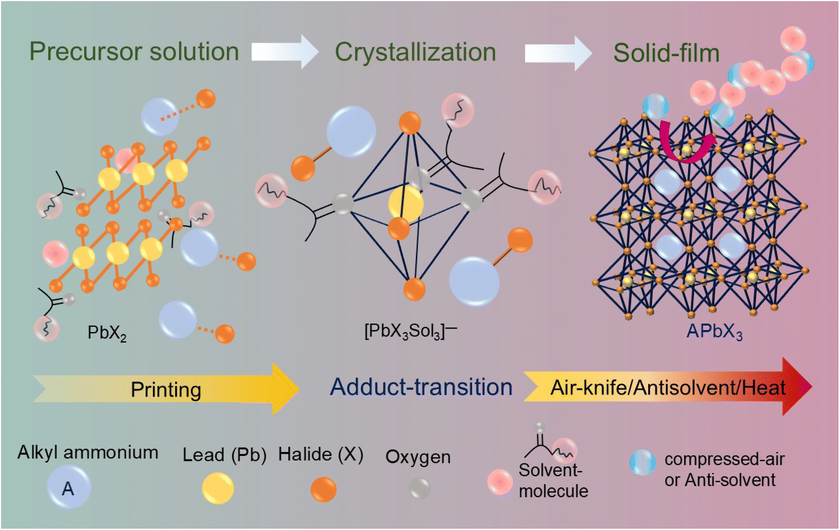 | ||
| Fig. 3 The schematic depicts the perovskite thin film formation from its solution phase. | ||
3. Large-scale deposition methods
Printed perovskite solar cells represent a promising avenue in the field of photovoltaics, combining the high efficiency potential of perovskite materials with the scalability and cost-effectiveness of printing techniques. These solar cells are fabricated by depositing of perovskite materials and other functional layers onto a substrate using various printing methods such as inkjet printing, screen printing, blade coating, or roll-to-roll coating. Inkjet printing, for example, enables precise droplet deposition, while screen printing allows for large-area patterning can be used for producing semi-transparent layers without chemical modifications for building-integrated photovoltaics (BIPVs). Whereas, the blade coating and slot-die coating offer continuous deposition over large areas. The Perovskite inks are formulated by dissolving perovskite precursors, such as lead halides and organic cations, in suitable solvents. Additives may be included to optimize ink properties, such as viscosity, surface tension, and drying behavior. Formulating stable and reproducible inks is essential for successful printing. Once the successful ink is formulated, the next step is printing the so + lar cell. Printing techniques allow for precise deposition of each layer, facilitating the fabrication of efficient solar cells. However, in recent times, the current research is highly focused on finding protocols of developing perovskite layer. This includes the development of stable perovskite compositions, interface engineering to improve moisture resistance, and the integration of advanced encapsulation techniques to protect against both moisture and heat-induced degradation, discussed below for every printing method.The importance of low-temperature processability has led to the use of multiple approaches for producing the PSCs. Thus, the perovskite precursors are used as inks suitable for printing/coating approaches. However, the perovskite morphology and crystallization is highly dependent on each method with processing conditions. Two different approaches can be used to fabricate the perovskite layer, in the first approach (contact method), this technique involves contact between the perovskite precursor and a sharp metal part of the instrument, thus the distance that is maintained between the substrate and the metal contact controls the perovskite layer thickness. In this contact approach, the perovskite layer will be grown from blade coating, roll-to-roll slot-die, and screen printing or mesh-assisted methods. Whereas in the second approach (non-contact method), there is no direct contact between the drying perovskite layer and the instrument. In this non-contact approach, the perovskite layer will be grown from spray coating, inkjet printing. Based on the required perovskite layer thickness, morphology, dimensional control and the feasibility, the contact or non-contact perovskite printing approach can be chosen. Both contact and non-contact approaches are schematically shown in the Fig. 4.
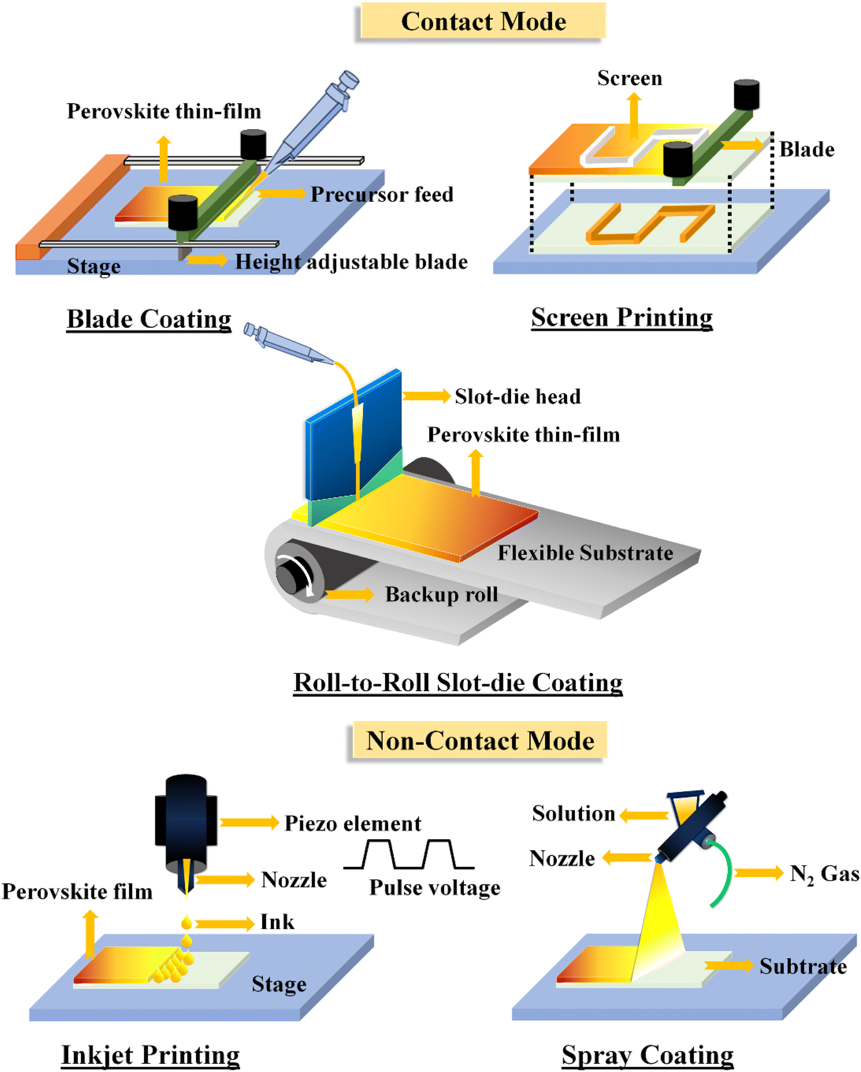 | ||
| Fig. 4 The diagram illustrates both contact and non-contact methods for applying a perovskite solution onto a substrate. | ||
In printing techniques, the key strategy is to apply materials during the critical adduct transition phase. Consequently, much of the research has focused on ink and solvent engineering. To optimize open-air printable methods for PSCs several innovations have emerged recently. These include solvent engineering, ink formulation, passivation strategies, modifications of the interfacial layers, improvements in deposition methods, and advancements in both pre-and post-deposition processes. The table below (Table 1) summarizes key findings from the literature concerning the development of various printing technologies. It specifically details the performance metrics of PSC configurations produced under open-air conditions, with efficiency parameters provided for each perovskite printing method.
| Device configuration | Printing method | Jsc (mA cm−2) | Voc (V) | FF (%) | Efficiency (%) | Progression | Substrate condition | Anti solvent treatment | References (year) |
|---|---|---|---|---|---|---|---|---|---|
| ITO/PTAA/PSK/PC70 BM/BCP/Ag perovskite:PSK (MA0.7 FA0.3 PbI3) | Blade coating: only PSK | 24.61 | 1.15 | 79.9 | 22.7 | Surface-treatment | RT, ambient air, RH ∼15 ± 5% | No | 43 (2024) |
| FTO/NiOx:Zn/PSK/PC61BM/BCP/Ag (PSK: MAPbCl3) | Blade coating: only PSK | 18.23 | 1.06 | 74.7 | 14.4 | Solvent-engineering | 150 °C, ambient air, RH% (NA) | No | 44 (2024) |
| Glass/ITO/SnO2/PSK/Spiro-OMeTAD/Au (PSK: Cd-FAPbI3) | Blade coating: SnO2, PSK and Spiro-OMeTAD. | 25.9 | 1.10 | 79.6 | 22.7 | Ink-engineering | RT, ambient air, RH ∼35% | No | 45 (2024) |
| FTO-glass/SnO2/PSK/carbon (PSK: FAPbBr3) | Blade coating: SnO2, PSK | 8.47 | 1.57 | 82.0 | 10.85 | In situ defect-passivation | RT, ambient air, RH ∼20 ± 5% | No | 46 (2024) |
| FTO/bTiO2/SnO2/PSK/Spiro-OMeTAD/Au (PSK: ((FAPbI3)0.95(MAPbBr3)0.05)) | Blade coating: SnO2, PSK | 23.8 | 1.16 | 85.0 | 23.4 | Ink-engineering | RT, ambient air, RH ∼25% | No | 47 (2023) |
| ITO/SnO2/PSK@KSCN/Spiro-OMeTAD/Au (PSK: MAPbI3) | Blade coating: PSK and Spiro-OMeTAD | 22 .62 | 1.116 | 80.8 | 20.40 | Ink-additive engineering (KSCN addition) | RT, ambient air, RH% (NA) | No | 48 (2023) |
| Glass/ITO/PTAA/PSK-SCW/PEACI/C60/BCP/Cu (PSK: MAPbI3) | Blade coating: only PSK | 22.75 | 1.11 | 80.0 | 20.05 | Ink-additive engineering (PEACI addition) | RT, ambient air, RH ∼30% | No | 49 (2023) |
| FTO/C–TiO2/TiO2/PSK/Spiro-OMETAD/Au (PSK: CH3NH3PbI3) | Blade coating: only PSK | 18.9 | 1.0 | 70.5 | 13.3 | Crystallization of PbI2 with air-flow | Air flow 100 °C, RH% (NA) | No | 50 and 51 (2023) |
| Glass/ITO/PTAA/PSK@BTACI/C60/BCP/Ag (PSK: MAPbI3) | Blade coating: only PSK | 22.5 | 1.13 | 81.3 | 20.5 | Additive assist-passivation technique, stability | RT, ambient air, RH of <50% | No | 51 and 52 (2022) |
| Glass/ITO/SAM/PSK/C60/BCP/Ag (PSK: MAPbI3) | Blade coating: only PSK | 21.5 | 1.08 | 79.2 | 18.4 | HTL surface engineering-improved perovskite wettability | RT, ambient air, RH of ≤50% | No | 52 (2022) |
| Glass/FTO/C–TiO2/mp TiO2/PSK/CB:Two bis(alkoxy)diphenylaminocarbazole/Ag (PSK: CH3NH3PbI3) | Blade coating: both PSK and HTL | 23.6 | 1.15 | 78.0 | 21.1 | Dopant-free HTL for printing techniques | 130 °C, ambient air, RH ∼30–40% | No | 53 (2022) |
| Glass/ITO/PEDOT:PSS/PSK/PCBM/BCP/Ag (PSK: CH3NH3PbI3) | Blade coating: PEDOT:PSS,PSK, PCBM and BCP | 21.1 | 1.02 | 69.1 | 14.1 | Buffer layer to block hole transfer | RT, ambient air, RH ∼35–50% | No | 54 (2020) |
| Glass/ITO/PSK + Me-4PACz/C60/(BCP)/Ag (PSK: Cs0.05 (FA0.98 MA0.02)0.95 Pb(I0.98Br0.02)3) | Blade coating: PSK + SAM | 23.88 | 1.16 | 81.23 | 22.1 | Co-deposition of perovskite and HTL | RT, ambient air, RH ∼40% | No | 55 (2023) |
| Glass/ITO/NiOx/SAM/PSK/PCBM/BCP/Ag (PSK: MAPbI3) | Spray coating: only PSK | 23.13 | 1.06 | 82.0 | 20.3 | Wettability/interfacial engineering | 40 °C, ambient air RH% (NA) | No | 56 (2024) |
| FTO/SnO2/PSK(n-propylammonium chloride)/PC61BM/Au (PSK: FAI/FABr/PACl) | Spray coating: only PSK | 20.33 | 1.17 | 81.6 | 19.42 | Additive engineering | RT, ambient air, RH ∼40% | No | 57 (2023) |
| PEN/ITO/PTAA/PSK/C60/BCP/Au (PSK: (CsPbI3)0.02(FA0.8 MA0.2Pb(I2.8 Br0.2))0.98) | Spray coating: only PSK | 22.4 | 1.06 | 75.7 | 18.04 | Uniform film on flexible substrate | 60 °C ambient air, RH% (NA) | No | 58 (2022) |
| FTO/c-TiO2/PSK/MoO2-with-5.0 wt% PTAA/carbon black (CB) submodule (PSK: CsPbI2Br) | Spray coating: all layers | 107.17 | 3.32 | 70.85 | 10.08 | Additive assist-wettability | 60 °C, ambient air, RH% (NA) | No | 59 (2022) |
| Glass/ITO/c-TiO2/m-TiO2/pervoskite/Spiro-oMeTAD/Au | Spray coating: Only PSK 2nd step | 19.11 | 0.91 | 56.0 | 9.86 | Defect formation mechanism | 50 °C, ambient air, RH% (NA) | No | 60 (2023) |
| ITO/PTAA/PSK/OMXene-CsPbI3 composite/CPTA/BCP/Ag (PSK: CsPbI3) | Spray coating: only PSK | 19.86 | 1.21 | 81.9 | 19.69 | Surface engineering | 170 °C, ambient air, RH% (NA) | No | 61 (2022) |
| ITO/NiOx/PSK/C60/BCP/Ag (PSK: CH3NH3PbI3) | Spray coating: only PSK | 22.04 | 1.00 | 80.0 | 17.43 | Additive assisted perovskite crystallization | Ambient air, 40 °C, RH% (NA) | No | 62 (2022) |
| Glass/ITO/c-TiO2/m-TiO2/PSK/Spiro-oMeTAD/Au (PSK: MAPbI3) | Spray coating: only PSK | 21.40 | 1.02 | 74.7 | 16.34 | Argon assisted spray coating | RT, ambient air, RH% (NA) | No | 63 (2022) |
| FTO/compact-TiO2/mp-TiO2/MAPbI3/mp-ZrO2/mp-carbon (PSK: MAPbI3) | Screen printing: TiO2, ZrO2, and carbon layers (PSK is dropped) | 24.31 | 0.93 | 68.12 | 15.39 | Additive -assisted perovskite crystallization | RT, ambient air, RH% (NA) | No | 64 (2023) |
| FTO/TiO2/ZrO2/PSK/carbon (PSK: FAPbI3) | Screen printing: TiO2, ZrO2, and carbon layers (PSK is dropped) | 22.08 | 1.02 | 76.0 | 17.11 | α/δ phase perovskite interface enhanced VOC | RT, ambient air, RH% (NA) | No | 65 (2022) |
| Glass/FTO/c-TiO2/PSK/ZrO2/C-layer (PSK: MAPbI3) | Screen printing: TiO2, ZrO2, and carbon layers (PSK is dropped) | 23.3 | 0.96 | 73.0 | 16.32 | Influenced precursor concentration | RT, ambient air, RH% (NA) | No | 66 (2020) |
| Glass/FTO/c-TiO2/ZrO2/C-layer/PSK (PSK: CH3NH3PbI3−xClx) | Screen printing: TiO2, ZrO2, and carbon layers (PSK is blade coated) | 20.01 | 0.96 | 60.0 | 11.53 | Compact layer deposited from chemical bath | 100 °C, ambient air, RH% (NA) | No | 67 (2019) |
| Glass/FTO/c-TiO2/TiO2/Al2O3/NiO/PSK/C (PSK: CH3NH3PbI3) | Screen printing: TiO2, Al2O3 and NiO layer (PSK is dip coated) | 21.62 | 0.91 | 76.0 | 15.03 | Additional NiO interlayer for charge separation | 70 °C, ambient air, RH% (NA) | No | 68 (2015) |
| FTO/compact-TiO2/mp-TiO2/mp-ZrO2/mp-carbon/PSK (PSK: MAI) | Screen printing: TiO2, ZrO2, and carbon layers (PSK is drop casted) | 24.3 | 0.97 | 65 | 15.4 | Low-temperature processed mp-carbon | RT, ambient air, RH ∼40% | No | 69 (2022) |
| FTO/compact-TiO2/mp-TiO2/mp-ZrO2/mp-carbon/FA-perovskite | Screen printing: TiO2,ZrO2 and carbon (PSK is drop casted) | 23.74 | 0.98 | 78 | 18.3 | Additive-assisted perovskite crystallization | RT, ambient air, RH% (NA) | No | 70 (2023) |
| ITO/SnO2/PSK/Spiro-OMeTAD/Au (PSK: PbI2 + FAI:MABr:MACl) | R2R: SnO2 and PSK | 21.31 | 1.09 | 72.9 | 16.87 | IPL for annealing | RT, ambient air, RH ∼20–30% | No | 71 (2024) |
| ITO-PET/SnO2/PSK/P3HT/C (PSK: MAPI) | R2R: SnO2, PSK and P3HT | 16.93 | 1.01 | 56.95 | 9.8 | Finding compatible HTL for carbon electrode | RT, ambient air, RH% (NA) | No | 72 (2024) |
| FTO/bl-TiO2/mp-TiO2/Na-TFSI/Perovskite/Spiro-OMeTAD/Au (module) | R2R: TiO2, PSK, and Spiro-OMeTAD | 2.55 | 10.25 | 76.29 | 19.9 | Additives, echo friendly solvents | RT, ambient air, RH% (NA) | No | 73 (2023) |
| ITO/SnO2/MAPI/PEDOT/carbon (PSK: MAPI) | R2R: All the layers | 20.91 | 0.89 | 65.1 | 13.26 | All roll-to-roll printed | RT, ambient air, RH% (NA) | No | 74 (2023) |
| ITO/PTAA/Ionogel-perovskite/choline chloride/C60/BCP/Cu | R2R: PTAA and PSK | 22.21 | 1.19 | 82.33 | 21.76 | Additive-assisted perovskite crystallization | 65 °C, ambient air, RH% (NA) | No | 75 (2022) |
| PET/TCE/SnO2/PSK/Spiro-OMeTAD/carbon/Ag (PSK: Cs0.05FA0.81 MA0.14Pb(I0.83 Br0.17)3) | R2R: SnO2, PSK and Spiro-OMeTAD | 20.9 | 1.17 | 68.1 | 16.7 | Vacuum and solvent-free | 17–21 °C, ambient air RH ∼30–60% | No | 76 (2022) |
| ITO glass/SnO2/PSK/Spiro-OMeTAD/Ag (PSK: CsPbI3) | R2R: SnO2, PSK and Spiro-OMeTAD | 21.45 | 1.0 | 60.59 | 13.0 | All roll-to-roll printed | 70 °C, ambient air, RH% (NA) | No | 77 (2022) |
| ITO/SnO2/PSK/Spiro-OMeTAD/Ag (PSK: FAPbI3) | Inkjet printing: Only PSK | 19.87 | 1.207 | 73.16 | 17.5 | Ink engineering | Ambient air, RT and RH ∼30–35% | No | 78 (2024) |
| ITO/SnO2/PSK/spiro-OMeTAD/Ag (PSK: CsFAMAPbBrxI3−x) | Inkjet printing: Only PSK | 18.32 | 1.187 | 77.73 | 16.90 | Focused on ETL | 23 °C, ambient air, RH ∼40% | No | 79 (2023) |
| PEN/ITO/NiOx/polymer pillar/PSK/PCBM/BCP/Ag (PSK: CS0.2FA0.8Pb(I0.6Br0.4)3) | Inkjet printing: polymer-pillar, and perovskite | 11.7 | 1.06 | 73.55 | 9.14 | Solvent engineering, digital control, flexible and semitransparent for BIPVs | Ambient air, RT, RH% (NA) | No | 38 (2023) |
| FTO/c-TiO2/m-TiO2/PSK/carbon (PSK: CsPbBr3) | Inkjet printing: only PSK | 7.36 | 1.51 | 81.7 | 9.09 | Device structural engineering | 60 °C, ambient air, RH ∼35% | No | 80 (2022) |
| FTO/TiO2/PSK/Spiro-OMeTAD/Au (PSK: MAPbI3/MAPbBr3) | Inkjet printing: only MAPbBr3 QDs | 21.69 | 1.21 | 75.0 | 17.06 | Intense pulse light sintering | RT, ambient air, RH% (NA) | No | 81 (2021) |
| PEN/AgNWs/PEDOT:PSS/PSK/PC71BM/PEI/Ag NWs (PSK: CH3NH3PbI3) | Inkjet printing: all the layers | 21.96 | 1.02 | 75.0 | 16.78 | All inkjet printing | 50 °C, ambient air, RH% (NA) | Yes (ethyl acetate fumes) | 82 (2021) |
| PET/IZO/PEDOT:PSS/PSK/C60/BCP/Ag (PSK: Cs0.1[(HC(NH2)2)0·83(CH3NH3)0.17]0.9 Pb (I0.83 Br0.17)3) | Inkjet printing: only PSK | 19.0 | 1.0 | 69.2 | 11.4 | Additive engineering, green solvent | RT, ambient air, RH ∼20–25% | No | 83 (2021) |
| FTO/TiO2/C60/Cs0.05MA0.14 FA0.81PbI2.55Br0.45/SpiroOMeTAD/Au. (PSK: Cs0.05MA0.14 FA0.81PbI2.55Br0.45) | Inkjet printing: only PSK | 23.48 | 1.108 | 76.2 | 19.6 | Ink engineering | RT, ambient air, and RH ∼25% | No | 84 (2020) |
| Glass/ITO/NiOx/TCP/PCBM/BCP/Au | Inkjet printing: all layers | 23.6 | 1.02 | 71.5 | 17.2 | All inkjet printed | RT, ambient air, and RH ∼45% | No | 85 (2020) |
For the fabrication of stable PSCs, the formulation of mixed cations and mixed halides has been widely reported as an effective strategy.86–88 This review examines key advancements in ink engineering, including perovskite formulations with additives, solvent optimization, surface treatments, and process innovations, all implemented across various open-air printing techniques are discussed below.
3.1. Blade-coating approach, advancement strategies
Blade coating, also known as the doctor-blading approach, involves depositing a thin layer of perovskite precursor solution onto a substrate using a moving blade apparatus. In blade coating, the thickness of the deposited film is determined by the gap between the blade and the substrate, as well as the properties of the solution, such as viscosity and surface tension. In the coating, the substrate will be placed over the stage then the perovskite precursor will be dropped, without further delay, a blade will be moved over the solution, to form a thin layer on top of the substrate. The concentration of the perovskite ink, blade moving speed, solvent evaporation rate etc., influences the quality of the perovskite film morphology. During this process, there is a precise control over the thickness of the solution deposited onto the substrate. Compared to Spin-coating, it has very low material waste and reduced manufacturing costs. This method can be also used to deposit various layers in the perovskite solar cell stack, including the perovskite absorber layer, HTL, and ETL. This versatility makes it a valuable technique for the fabrication of multi-layered devices. However, there are a few challenges, perovskite precursor solutions need to be carefully formulated to ensure stability during the coating process. Achieving optimal coating conditions requires careful optimization of parameters such as solution concentration, coating speed, blade geometry, and substrate temperature. Variations in these parameters can affect film morphology, crystallinity, and device performance. Here we focus on the improvements achieved by incorporating additives, engineering solvents, and utilizing low-dimensional perovskites via blade-coating approach.The key challenges in this method lie in optimizing the perovskite ink to achieve the appropriate wettability and in stabilizing the perovskite film under open-air conditions. This includes high-end crystallization process, protecting the surface of the blade-coated perovskite layer making it rigid towards moisture air, and thus the required interfacial engineering, and ink-engineering techniques, which are critically examined based on recent advancements in the literature.
In the air-blade-assisted deposition method (Fig. 5a), nitrogen (N2) is applied with constant pressure in the direction of the substrate's movement immediately after the perovskite layer is deposited via blade coating. The airflow serves to dynamically remove solvent molecules, facilitating the formation of a perovskite layer with enhanced crystallinity. This approach resulted in perovskite films with larger grain sizes, the surface view seen from scanning electron microscopy (SEM) images, compared to those produced by spin-coating (see Fig. 5b and c). XRD analysis also supports the air-blade technique, showing narrower FWHM values relative to spin-coating, indicating improved crystallinity. Furthermore, devices produced with air-knife-assisted deposition demonstrate enhanced stability (Fig. 5e).
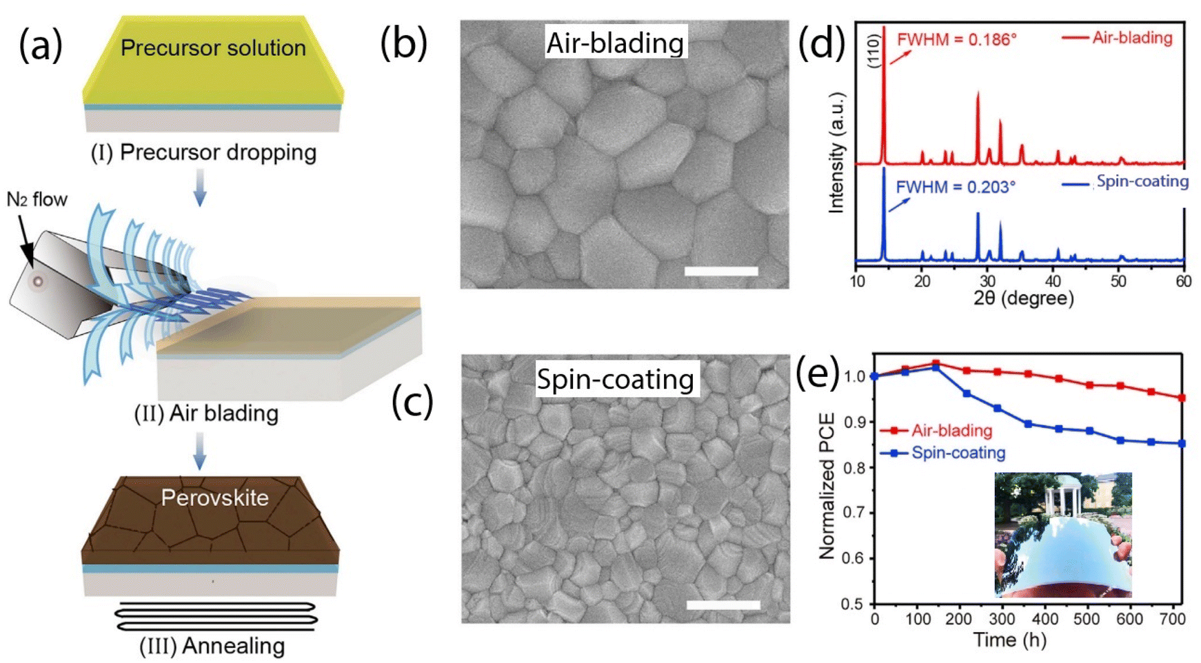 | ||
| Fig. 5 (a) Schematic illustration of perovskite film deposition using the air-knife-assisted approach. (b and c) Top-view SEM images of perovskite (MAPbI3) films deposited by air-knife (b) and spin-coating (c) methods, showcasing the differences in grain structure. (d) XRD patterns of MAPbI3 films, highlighting crystallinity improvements with the air-knife technique. (e) Stability comparison for solar cells made with each method; the inset displays a 15 cm × 15 cm perovskite module. This figure has been adapted from ref. 89 with permission from Elsevier, copyright 2018. | ||
The study found that the distribution of PCBM was influenced by the additive, which also caused a significant change in the zeta potential. The EVA additive further prevented the diffusion of halide ions through the ETL, as illustrated in Fig. 6. As a result, the blade-coated device achieved a PCE of 19.32%, with 80% retention of its initial efficiency after 1500 hours of storage under ambient conditions (52% humidity), notably without encapsulation. Additionally, when the active area of the solar cell was increased to 25 cm2, a PCE of over 10% was reported. Thus, the use of EVA significantly enhanced the blade-coating method for PSC fabrication.90
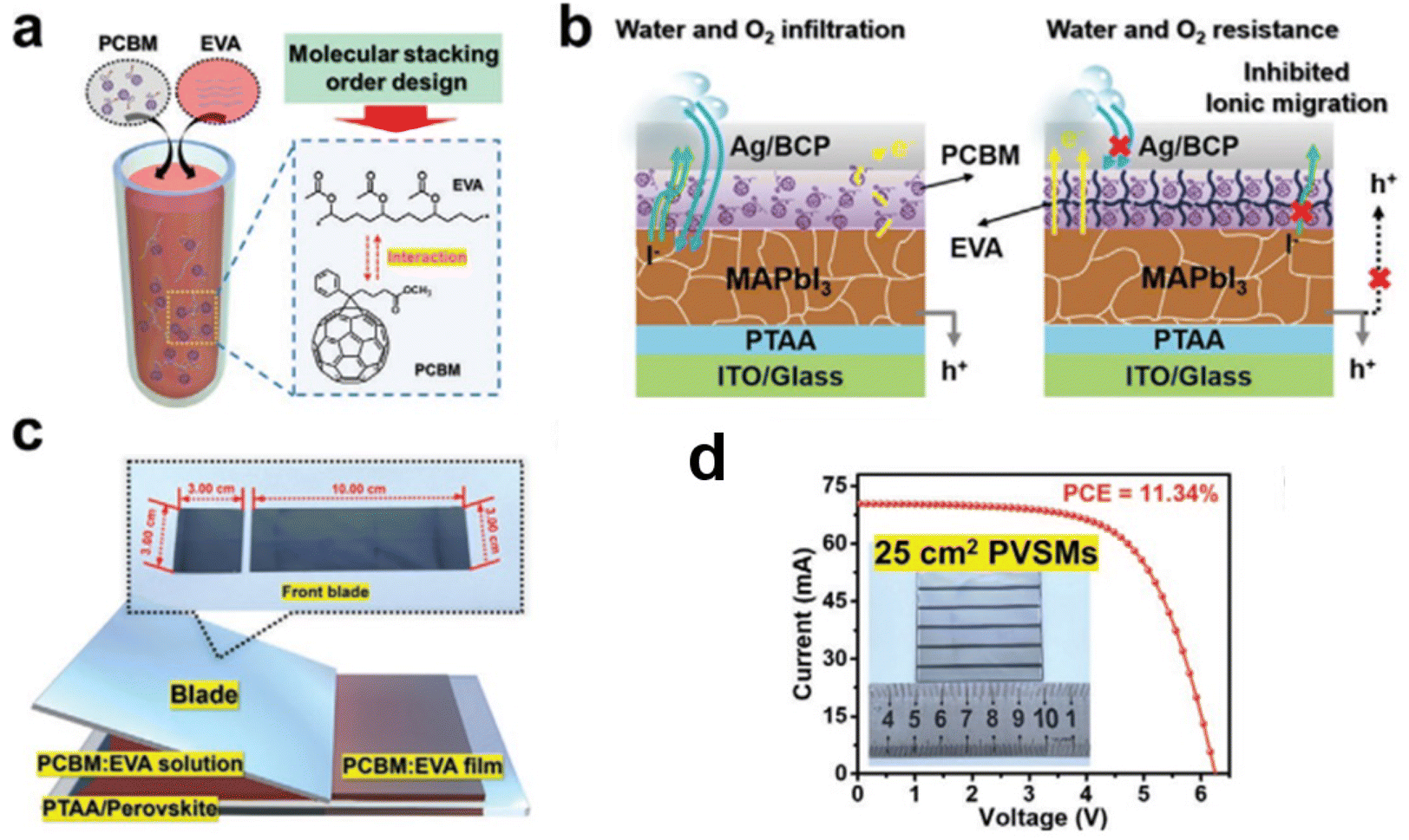 | ||
| Fig. 6 (a) Schematic illustration depicting the molecular stacking order regulation of PCBM with the addition of an EVA (ethylene-vinyl acetate) additive. (b) Diagram of PSC utilizing a PCBM-EVA ETL, highlighting improved charge transfer capability, enhanced water and oxygen barrier properties, and reduced ion migration. (c) Schematic showing the blade-coated PCBM buffer layer incorporating EVA additive. (d) Current density–voltage (J–V) curves of the larger-area PSC module based on the PCBM ETL with best efficiency. This figure has been adapted from ref. 90 with permission from John Wiley and Sons, copyright 2021. | ||
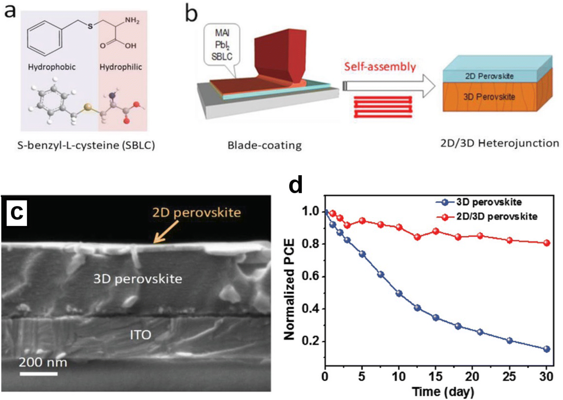 | ||
| Fig. 7 SBLC molecular structure (a); the blade-coating of the 2D/3D perovskite film schematic (b); SEM surface images of the 2D/3D perovskite film (c); shelf stability of the 3D and 2D/3D heterostructure solar cells stored in ambient air with a relative humidity (RH) of 50% ± 10% (d). This figure has been adapted from ref. 94 with permission from John Wiley and Sons, copyright 2020. | ||
Thus, in the blade coating approach, all the above strategies are employed in recent times for the fabrication of large-scale modules in open-air conditions as we have discussed above, and the attention to be paid for further development of the high efficient PSCs of reduced chemical toxicity.
3.2. Roll-to-roll slot-die printing approach, advancement strategies
This approach is commonly referred to as roll-to-roll (R2R) printing or the R2R-based slot-die printing technique. Similar to R2R, flexographic printing and gravure printing are two additional techniques that operate in a comparable manner. However, due to its suitability for versatility, and higher resolution printing, R2R is specifically utilized for PSCs.101 R2R processing is a high-throughput manufacturing technique that involves the continuous fabrication of flexible electronic devices on a roll of flexible substrate material, such as plastic or metal foil. Ensuring compatibility with perovskite materials and deposition processes is crucial to achieving high-quality devices. Maintaining precise control over deposition parameters such as coating speed, temperature, and atmosphere in a continuous roll-to-roll environment can be challenging. Variations in these parameters can affect film quality, device performance, and yield. R2R processing holds great promise for the scalable production of flexible perovskite solar cells. In a conventional roll-to-roll slot-die approach, there will be a slot-die coater, where the perovskite will be coated and then the substrate will be passed through a compressed air flow, followed by passing through a thermal heater which leads the perovskite crystallization. However, the drying process is often ineffective in producing high-quality perovskite films. As a result, researchers are actively seeking alternative methods to improve the fabrication process.3.2.1.1 Infrared pulsed light (IPL) annealing treatment. In 2018, Michael Saliba and his team pioneered the Infrared Pulsed Light (IPL) Annealing treatment, a breakthrough technique specifically designed for halide perovskites with a high level of phase purity, which has significantly advanced the efficiency and stability of these materials in solar cell applications.102
In 2024, Dong Seok Ham's research group made significant progress in understanding the phase purity of perovskite layers within the realm of ink engineering. Their study focused on incorporating cesium salts, such as cesium iodide (CsI) and cesium formate (CsF), into the PbI2 solution. This approach notably improved the preservation of phase purity in the perovskite layer, particularly when combined with formamidinium iodide (FAI) and followed by IPL annealing treatments. As illustrated in Fig. 8, this innovative ink engineering method resulted in a higher-quality perovskite layer, with IPL treatments yielding better outcomes compared to conventional thermal drying methods.71
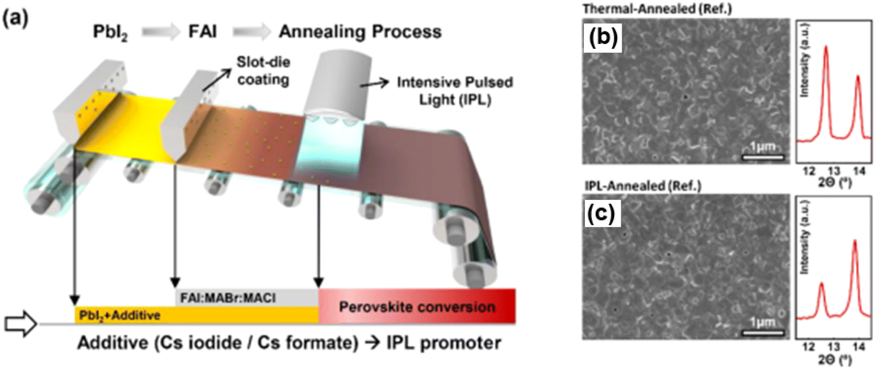 | ||
| Fig. 8 Schematic representation of the R2R two-step processing method utilizing an IPL treatment (a); FE-SEM and XRD graphs of the perovskite surface (pristine PbI2) (b); FE-SEM and XRD (pristine PbI2) analysis of perovskite surfaces treated with IPL (c). This figure has been adapted from ref. 71 with permission from American Chemical Society, copyright 2024. | ||
3.2.1.2 Dry press deposition (DPD). The fabrication of fully printed perovskite solar cells (PSCs) necessitates the careful addition of a top contact layer, which plays a critical role in achieving proper ohmic contact. A major challenge in this process is protecting the sensitive perovskite layer from damage, particularly due to solvent exposure. Additionally, the use of vacuum-assisted metal deposition significantly drives up the cost of solar cell technology. To address these challenges, Hasitha W.'s team developed a novel approach that involves mechanically pressing the top contact onto the device without the need for solvents (Fig. 9). This technique significantly reduces the risk of solvent-induced damage, making it a promising innovation in PSC fabrication. However, the success of this method hinges on the precise optimization of pressing conditions to ensure that the fragile perovskite layer remains undisturbed. Furthermore, the exceptional bending durability of flexible PSCs with printed DPD electrodes underscores their potential for various flexible electronic applications. This approach represents a crucial advancement towards the commercial viability of PSCs, offering a cost-effective, vacuum-free, and solvent-free alternative to the traditionally expensive evaporative deposition of metal electrodes. Such innovations are pivotal in driving the widespread adoption and practical implementation of perovskite solar technology.103
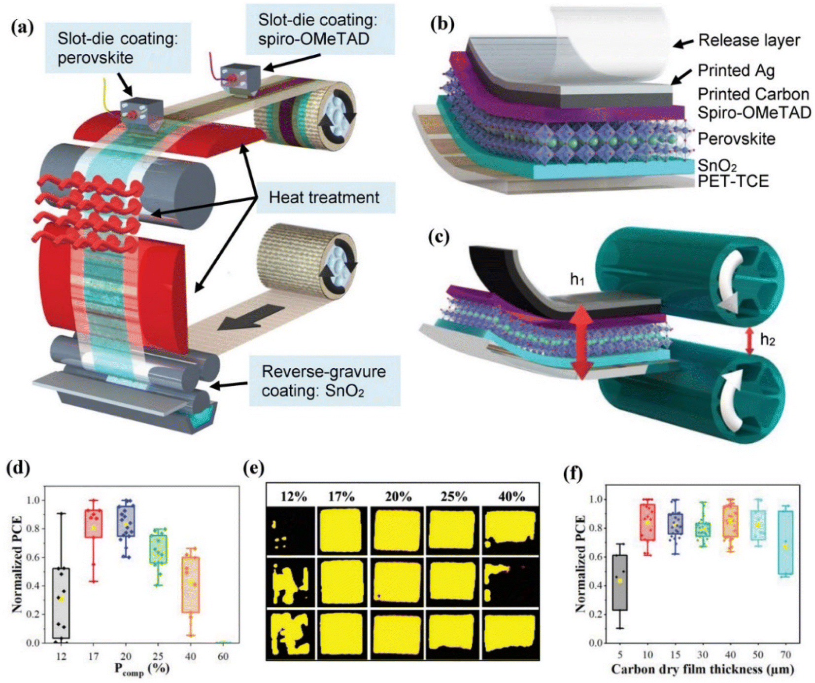 | ||
| Fig. 9 The diagram illustrates the R2R fabrication process for the PSC precursor stack (a); the PSC device architecture is depicted, highlighting the release layer mechanism that facilitates the removal of the device from the substrate (b); the Dry Press Deposition (DPD) process is shown alongside the equation used to calculate the compressive pressure applied during fabrication (c); a graph displays the normalized PCE results for devices fabricated under varying levels of compression pressure, illustrating the impact of pressure on device performance (d); light-beam induced current (LBIC) maps provide a visual representation of PSCs fabricated at different compressive pressures, indicating how pressure variations affect the uniformity and performance of the cells (e); another graph presents the normalized PCE results for devices fabricated with varying carbon film thicknesses, demonstrating the relationship between carbon layer thickness and overall device efficiency (f). This figure has been reproduced from ref. 103 with permission from John Wiley and Sons, copyright 2022. | ||
3.3. Screen-print or mesh-assisted perovskite deposition, advancements
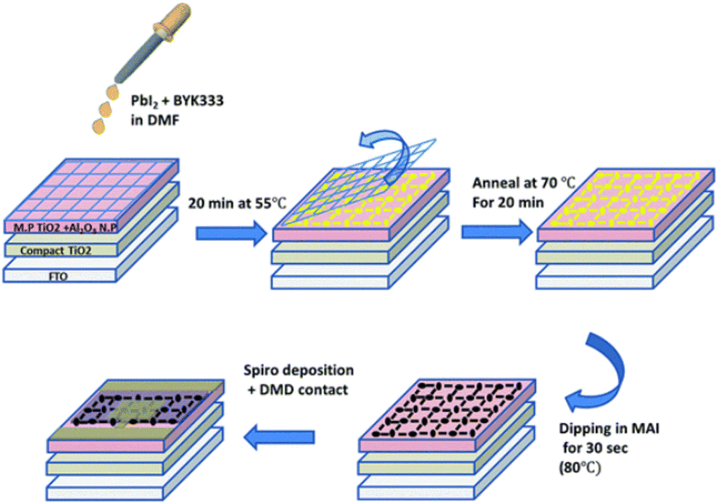
The screen-printing technique excels in rapidly coating micrometer-thick films over large areas, leveraging a screen or mesh as a support structure. These screens, often crafted from durable polymer materials, are resistant to the chemicals used during the process. As a result, this method yields highly uniform films and enables efficient production on a large scale, with the ability to achieve rapid processing times.The mesh size and precursor concentration are critical factors in tuning the film's transparency and thickness. The non-viscous nature of the perovskite solution enables it to spread uniformly over the mesh, forming a grid structure with voids that are later covered by a thin perovskite layer. The crystallization of the perovskite layer, and thus the device's efficiency, is further controlled by adding surfactants and adjusting the substrate temperature. Mixed cation and halide perovskite formulations have shown excellent stability and efficiency with this approach. Initially, perovskite grid-based solar cells achieved PCEs of around 5% with an average visible transparency (AVT) of 30%. Through compositional modifications and a refined 1.5-step deposition process (seen in Fig. 10), PCEs were later increased to 10%, with a slightly reduced AVT of 28%. This technique demonstrates significant potential for developing high-performance, semi-transparent PSCs for building-integrated applications.106
 | ||
| Fig. 10 Schematic illustration of the perovskite grid formation using the mesh-assistance method. This figure has been reproduced from ref. 105 with permission from Royal Society of Chemistry, copyright 2016. | ||
3.4. Ink-jet printing, advancements
Inkjet printing has garnered considerable attention in the fabrication of PSCs due to its advantages in low-cost, scalable production and precise material deposition. This technique minimizes material wastage by applying only the necessary amount of perovskite solution onto the substrate, which helps reduce costs associated with material consumption. Inkjet printing's non-contact nature enables precise patterning of films by controlling droplet deposition and allows for the incorporation of other functional materials into the perovskite layer at specific locations and quantities. Furthermore, inkjet printing is more environmentally friendly, as it releases fewer solvents into the environment compared to other printing technologies. Despite these benefits, there are notable challenges in using inkjet printing for perovskite solar cells. Developing stable, high-quality perovskite inks that are compatible with inkjet printing is crucial, requiring careful control of ink stability, viscosity, and overall compatibility with the printing process. Additionally, managing the crystallization of printed perovskite is essential to achieve the desired morphology and optoelectronic properties. After the perovskite precursor is printed, the film undergoes a crystallization process, typically involving vacuum treatment followed by heat treatment at carefully controlled temperatures as discussed below. Rapid ink drying can result in non-uniform film formation and defects, impacting the performance and reliability of the solar cells. These subsequent processing steps ensure the formation of a high-quality perovskite layer with optimal structural and optoelectronic properties. However, challenges also remain with the chemical compatibility of the printer's head. The efficiency of inkjet printing also depends on the viscosity and chemical behavior of the solvents used, and clogging of any nozzles can cause significant damage to the entire solar cell.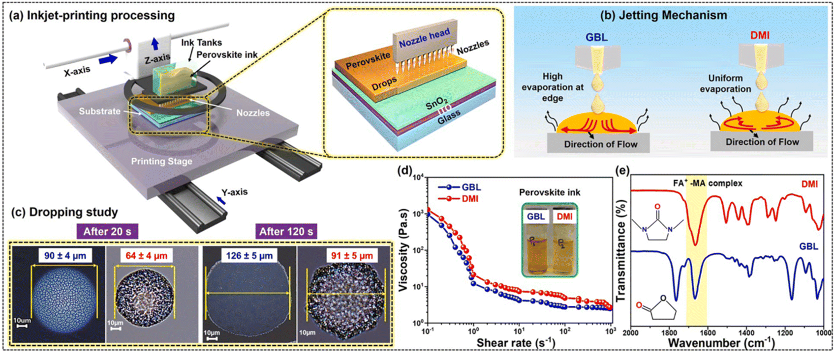 | ||
| Fig. 11 Schematic representation of the inkjet-printed perovskite film fabrication process, illustrating the steps involved from inkjet deposition to film formation (a); diagram depicting the jetting mechanism of perovskite ink formulated with GBL and DMI, detailing how these solvents influence ink ejection and patterning (b); graph showing the perovskite ink drop spreading rate over time, measured at 20 seconds and 120 seconds post-printing, highlighting the ink's behavior as it settles and spreads on the substrate (c); plot of the viscosity of GBL and DMI-based perovskite inks as a function of shear rate, demonstrating how the ink's viscosity changes under different shear conditions (d); FTIR analysis of perovskite inks prepared with GBL and DMI solvents, providing insights into the chemical composition and interactions within the inks (e). This figure has been reproduced from ref. 107 with permission from Elsevier, copyright 2024. | ||
Extensive research has been conducted on utilizing inkjet printing technology for fabricating fully printed PSCs. In a 2021 study, Ulrich and his team reported the development of a p-i-n structured PSC using a triple cation perovskite formulation. This innovative design achieved a reported efficiency of over 17%. The uniformity of the layers within this structure is illustrated in Fig. 12. The authors emphasized that controlling wettability plays a crucial role in enhancing both the stability and efficiency of the device.108
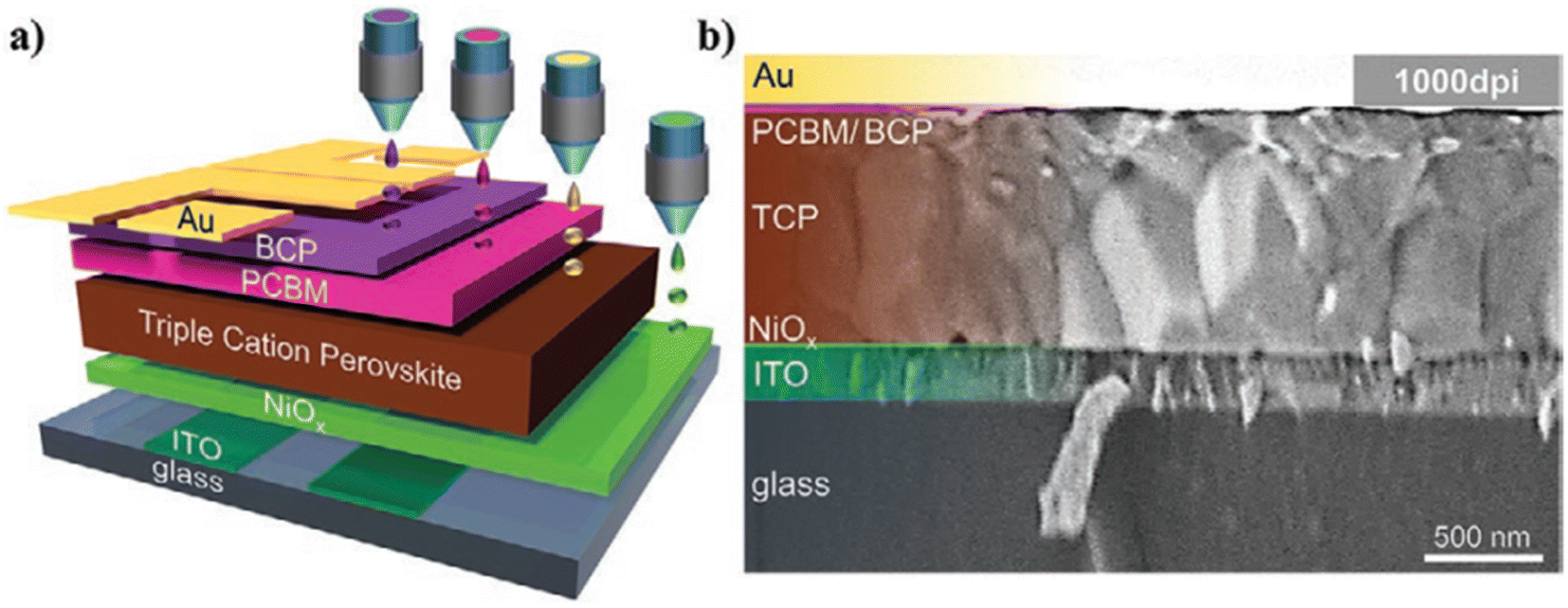 | ||
| Fig. 12 Schematic illustration of the p-i-n perovskite solar cell architecture featuring all printed layers (a). The SEM image showing a cross-section of the device (b). This figure has been adapted from ref. 108 with permission from John Wiley and Sons, copyright 2020. | ||
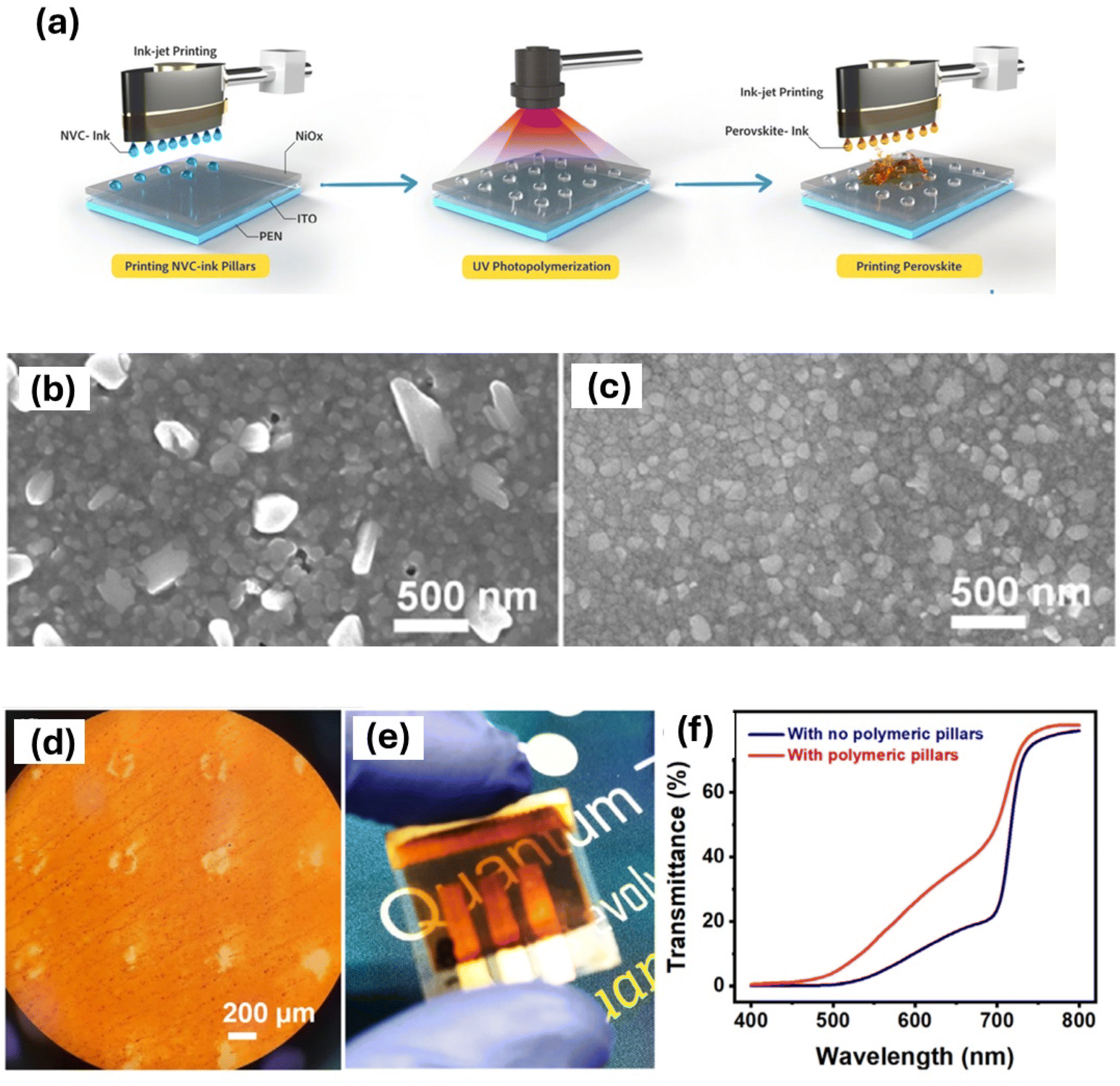 | ||
| Fig. 13 The ink-jet printing of monomer and polymerization under UV light, followed by deposition of a perovskite layer over a flexible substrate (a). The surface SEM images of the inkjet-printed perovskite are shown without surfactant (b) and with surfactant (c). Additionally, the optical image of the polymer pillar-integrated perovskite film is presented in (d), alongside the transparent, flexible PSC (e), and the optical transparency comparison of the PSC with and without polymer pillar integration is displayed in (f). This figure has been adapted from ref. 38 with permission from John Wiley and Sons, copyright 2023. | ||
While inkjet-printed PSCs have demonstrated promising efficiencies, further optimization is necessary to enhance device performance, stability, and long-term environmental resilience.
3.5. Spray-coating, advancements
Spray coating is another promising technique for fabricating perovskite solar cells, in this method, a solution containing perovskite precursors is atomized and sprayed onto a substrate, forming a thin film upon drying. Proper optimization of spray parameters, such as nozzle size, spray distance, solution concentration, and substrate temperature, is crucial for achieving uniform perovskite films with controlled thickness and morphology. As such, a diluted precursor solution is sprayed over the substrate at room temperature or at desired temperatures. Currently, spraying is often done manually, but mechanical sprayers can achieve spatial uniformity.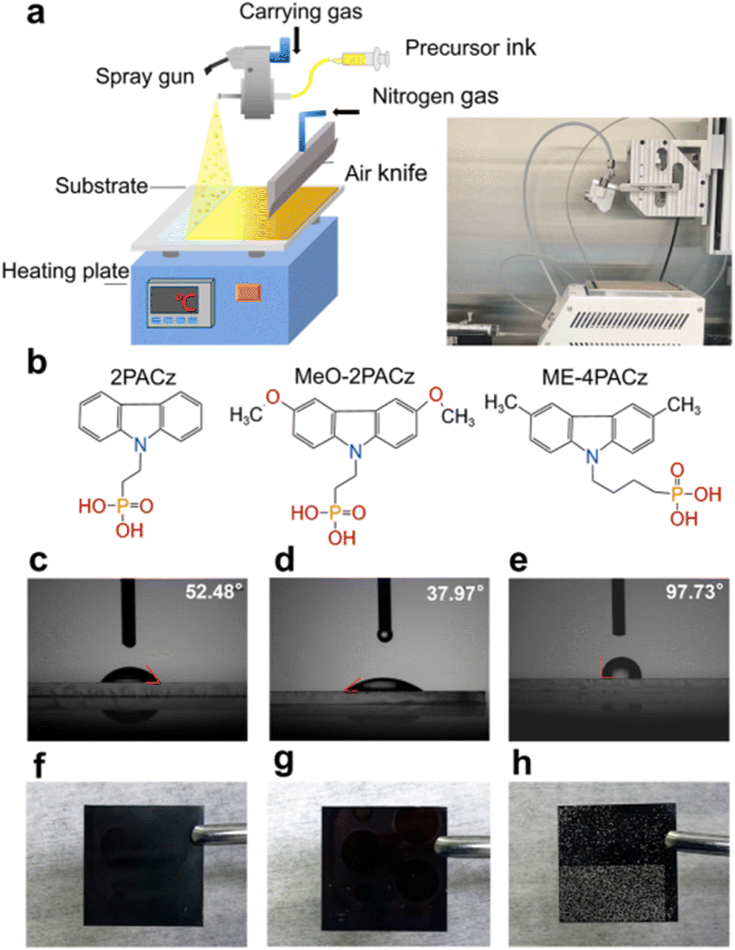 | ||
| Fig. 14 Schematic illustration and photograph of perovskite film fabrication using the ultrasonic spray-coating method (a); molecular structures of 2PACz, Me-4PACz, and MeO-2PACz (b); contact angles of the precursor solution on 2PACz, (c); MeO-2PACz, (d); and Me-4PACz (e); images of the perovskite film sprayed on 2PACz, (f); MeO-2PACz, (g); and Me-4PACz (h). This figure has been reproduced from ref. 111 with permission from American Chemical Society, copyright 2024. | ||
4. Conclusions and challenges
Perovskite solar cells are in high demand for commercialization. The focus should be on fabricating larger PSCs with improved lifetime at a lower cost using less-toxic approaches. Printable approaches, such as blade-coating, ink-jet printing, slot-die approach, spray-coating, and screen-printing, are useful for constructing solar cells in open-air conditions that could produce larger-area modules. Each approach presents its own benefits and challenges. The R2R process, for example, is limited by flexible substrates, while inkjet printing struggles with chemical and coagulation issues that affect jetting. Spray coating encounters spatial uniformity problems, and screen printing often results in poor perovskite crystallization. However, many of these challenges are being addressed. Additives in perovskites have been shown to enhance crystallization and morphology, surface treatments improve wettability, and low-dimensional perovskites boost device stability. Furthermore, simplifying processes and modifying device structures have proven effective in improving optical properties. Thus, in this review, we have discussed the literature on printing PSCs, with improved properties, including PSCs with more advanced and simplified fabrications, and with digital control over the semitransparency for BIPVs, etc. It is important to note that the chemical compositions of the hybrid perovskite materials and solvents should be less toxic in particular when working in open air. While most open-air processing currently focuses on Pb-based perovskites, directing printable approaches toward the development of Pb-free PSCs offers promising potential. Additionally, it is important to highlight that employing open-air techniques for constructing all layers is crucial for the successful production of PSC modules. Equally significant is the need to recycle PSCs to mitigate the adverse environmental effects of the materials used.Data availability
No primary research results, software or code have been included and no new data were generated or analysed as part of this review.Conflicts of interest
There are no conflicts to declare.Acknowledgements
PNK would like to acknowledge the valuable assistance of ChatGPT, in refining the clarity of the manuscript. PNK thanks the María Zambrano Talent Postdoctoral Fellowship, Spanish Ministry of Universities, supported by the European Union's Next Generation EU funds (MAZ/2021/02). AG is grateful for grant PID2022-141850OB-C21 funded by MICIU/AEI/10.13039/501100011033 and by ERDF/EU.References
- H. H. Pourasl, R. V. Barenji and V. M. Khojastehnezhad, Energy Rep., 2023, 10, 3474–3493 CrossRef.
- T. G. Allen, J. Bullock, X. Yang, A. Javey and S. De Wolf, Nat. Energy, 2019, 4, 914–928 CrossRef CAS.
- A. Richter, R. Müller, J. Benick, F. Feldmann, B. Steinhauser, C. Reichel, A. Fell, M. Bivour, M. Hermle and S. W. Glunz, Nat. Energy, 2021, 6, 429–438 CrossRef CAS.
- L. C. Andreani, A. Bozzola, P. Kowalczewski, M. Liscidini and L. Redorici, Adv. Phys.:X, 2019, 4, 1548305 CAS.
- M. S. Seetharaman, P. Nagarjuna, P. N. Kumar, S. P. Singh, M. Deepa and M. A. G. Namboothiry, Phys. Chem. Chem. Phys., 2014, 16, 24691–24696 RSC.
- J. J. Yoo, G. Seo, M. R. Chua, T. G. Park, Y. Lu, F. Rotermund, Y. K. Kim, C. S. Moon, N. J. Jeon, J. P. Correa-Baena, V. Bulović, S. S. Shin, M. G. Bawendi and J. Seo, Nature, 2021, 590, 587–593 CrossRef CAS PubMed.
- M. Jeong, I. Woo Choi, E. Min Go, Y. Cho, M. Kim, B. Lee, S. Jeong, Y. Jo, H. Won Choi, J. Lee, J.-H. Bae, S. Kyu Kwak, D. Suk Kim and C. Yang, Science, 2020, 369, 1615–1620 CrossRef CAS PubMed.
- S. Mahesh, J. M. Ball, R. D. J. Oliver, D. P. McMeekin, P. K. Nayak, M. B. Johnston and H. J. Snaith, Energy Environ. Sci., 2020, 13, 258–267 RSC.
- L. Gil-Escrig, C. Dreessen, F. Palazon, Z. Hawash, E. Moons, S. Albrecht, M. Sessolo and H. J. Bolink, ACS Energy Lett., 2021, 6, 827–836 CrossRef CAS PubMed.
- M. S. G. Hamed and G. T. Mola, Crit. Rev. Solid State Mater. Sci., 2019, 45(2), 85–112 CrossRef.
- T. Yang, L. Gao, J. Lu, C. Ma, Y. Du, P. Wang, Z. Ding, S. Wang, P. Xu, D. Liu, H. Li, X. Chang, J. Fang, W. Tian, Y. Yang, S. Liu and K. Zhao, Nat. Commun., 2023, 14, 839 CrossRef CAS PubMed.
- J. J. Yoo, S. S. Shin and J. Seo, ACS Energy Lett., 2022, 7, 2084–2091 CrossRef CAS.
- P. N. Kumar, A. Das, A. Kolay and M. Deepa, Mater. Adv., 2022, 3, 2249–2267 RSC.
- A. Kolay, P. N. Kumar, S. K. Kumar and M. Deepa, Phys. Chem. Chem. Phys., 2017, 19, 4607–4617 RSC.
- P. N. Kumar, A. Kolay, M. Deepa, S. M. Shivaprasad and A. K. Srivastava, ACS Appl. Mater. Interfaces, 2017, 9, 25278–25290 CrossRef CAS PubMed.
- R. K. Kokal, P. Naresh Kumar, M. Deepa and A. K. Srivastava, J. Mater. Chem. A, 2015, 3, 20715–20726 RSC.
- P. N. Kumar, S. Mandal, M. Deepa, A. K. Srivastava and A. G. Joshi, J. Phys. Chem. C, 2014, 118, 18924–18937 CrossRef CAS.
- P. N. Kumar, A. Kolay, S. K. Kumar, P. Patra, A. Aphale, A. K. Srivastava and M. Deepa, ACS Appl. Mater. Interfaces, 2016, 8, 27688–27700 CrossRef CAS PubMed.
- P. N. Kumar, A. Das and M. Deepa, J. Alloys Compd., 2020, 154880, DOI:10.1016/j.jallcom.2020.154880.
- P. N. Kumar, A. Kolay, S. K. Kumar, P. Patra, A. Aphale, A. K. Srivastava and M. Deepa, ACS Appl. Mater. Interfaces, 2016, 8, 27688–27700 CrossRef CAS PubMed.
- R. Narayanan, P. N. Kumar, M. Deepa and A. K. Srivastava, Electrochim. Acta, 2015, 178, 113–126 CrossRef CAS.
- P. N. Kumar, M. Deepa and A. K. Srivastava, Phys. Chem. Chem. Phys., 2015, 17, 10040–10052 RSC.
- P. N. Kumar, A. Das, M. Deepa, P. Ghosal and A. K. Srivastava, ChemistrySelect, 2016, 1, 5320–5330 CrossRef CAS.
- P. N. Kumar, R. Narayanan, M. Deepa and A. K. Srivastava, J. Mater. Chem. A, 2014, 2, 9771–9783 RSC.
- P. Subramanyam, P. Naresh Kumar, M. Deepa, C. Subrahmanyam and P. Ghosal, Sol. Energy Mater. Sol. Cells, 2017, 159, 296–306 CrossRef CAS.
- P. N. Kumar, R. Narayanan, S. Laha, M. Deepa and A. K. Srivastava, Sol. Energy Mater. Sol. Cells, 2016, 153, 138–147 CrossRef CAS.
- Y. Zheng, Y. Li, R. Zhuang, X. Wu, C. Tian, A. Sun, C. Chen, Y. Guo, Y. Hua, K. Meng, K. Wu and C.-C. Chen, Energy Environ. Sci., 2024, 17, 1153–1162 RSC.
- F. Zheng, C. Zuo, M. Niu, C. Zhou, S. J. Bradley, C. R. Hall, W. Xu, X. Wen, X. Hao, X. Hao, M. Gao, T. A. Smith and K. P. Ghiggino, ACS Appl. Mater. Interfaces, 2020, 12, 25980–25990 CrossRef CAS PubMed.
- T. Zhu, Y. Yang, K. Gu, C. Liu, J. Zheng and X. Gong, ACS Appl. Mater. Interfaces, 2020, 12, 51744–51755 CrossRef CAS PubMed.
- J. Hu, I. W. H. Oswald, S. J. Stuard, M. M. Nahid, N. Zhou, O. F. Williams, Z. Guo, L. Yan, H. Hu, Z. Chen, X. Xiao, Y. Lin, Z. Yang, J. Huang, A. M. Moran, H. Ade, J. R. Neilson and W. You, Nat. Commun., 2019, 10(1–11), 1276 CrossRef PubMed.
- X. Zhang, G. Wu, W. Fu, M. Qin, W. Yang, J. Yan, Z. Zhang, X. Lu and H. Chen, Adv. Energy Mater., 2018, 8(1–9), 1702498 CrossRef.
- Y. Wang, W. Chen, L. Wang, B. Tu, T. Chen, B. Liu, K. Yang, C. W. Koh, X. Zhang, H. Sun, G. Chen, X. Feng, H. Y. Woo, A. B. Djurišić, Z. He and X. Guo, Adv. Mater., 2019, 31, 1–10 Search PubMed.
- Y. W. Jang, S. Lee, K. M. Yeom, K. Jeong, K. Choi, M. Choi and J. H. Noh, Nat. Energy, 2021, 6, 63–71 Search PubMed.
- P. Naresh Kumar and L. Etgar, Two-Dimensional and Three-Dimensional (3D) Perovskite Structures for Robust and Efficient Solar Cell Fabrication, Nanomaterials for Energy Applications, CRC Press, 1st edn, 2023 Search PubMed.
- Y. Nakamura, N. Shibayama, K. Fujiwara, T. Koganezawa and T. Miyasaka, ACS Mater. Lett., 2022, 4, 2409–2414 CrossRef CAS.
- D. Zhang, D. Li, Y. Hu, A. Mei and H. Han, Commun. Mater., 2022, 3, 58 CrossRef.
- Y. Tang, Y. Zhang, X. Zhou, T. Huang, K. Shen, K. N. Zhang, X. Du, T. Shi, X. Xiao, N. Li, C. J. Brabec, Y. Mai and F. Guo, Nano Energy, 2023, 108653, DOI:10.1016/j.nanoen.2023.108653.
- N. K. Pendyala, S. Magdassi and L. Etgar, Sol. RRL, 2023, 2200988, DOI:10.1002/solr.202200988.
- J. W. Yoo, J. Jang, U. Kim, Y. Lee, S. G. Ji, E. Noh, S. Hong, M. Choi and S. Il Seok, Joule, 2021, 5, 2420–2436 CrossRef CAS.
- A. D. Taylor, Q. Sun, K. P. Goetz, Q. An, T. Schramm, Y. Hofstetter, M. Litterst, F. Paulus and Y. Vaynzof, Nat. Commun., 2021, 1878, DOI:10.1038/s41467-021-22049-8.
- E. Radicchi, E. Mosconi, F. Elisei, F. Nunzi and F. De Angelis, ACS Appl. Energy Mater., 2019, 2, 3400–3409 CrossRef CAS.
- D. Shen, X. Yu, X. Cai, M. Peng, Y. Ma, X. Su, L. Xiao and D. Zou, J. Mater. Chem. A, 2014, 2, 20454–20461 RSC.
- J. Zhuang, C. Liu, B. Kang, H. Cheng, M. Xiao, L. Li and F. Yan, Adv. Mater., 2024, 2309869, DOI:10.1002/adma.202309869.
- H. Yu and B. Cao, New J. Chem., 2024, 13342, 10.1039/d4nj01972e.
- D. Zhang, S. Khasnabis, W. Wang, V. Yeddu, S. Moradi, M. Awais, H. D. Nguyen, S. B. Reinecke, Y. Haruta, R. Godin, F. Tan and M. I. Saidaminov, Adv. Energy Mater., 2024, 2303858, DOI:10.1002/aenm.202303858.
- H. Yang, T. Zhou, H. Cai, W. Shen, H. Chen, Y. Liu, J. Zhao, Y. B. Cheng and J. Zhong, J. Energy Chem., 2024, 96, 396–405 CrossRef CAS.
- J. Chung, S. W. Kim, Y. Li, T. Mariam, X. Wang, M. Rajakaruna, M. M. Saeed, A. Abudulimu, S. S. Shin, K. N. Guye, Z. Huang, R. J. E. Westbrook, E. Miller, B. Subedi, N. J. Podraza, M. J. Heben, R. J. Ellingson, D. S. Ginger, Z. Song and Y. Yan, Adv. Energy Mater., 2023, 2300595, DOI:10.1002/aenm.202300595.
- Z. Zhang, J. Shang, H. Ge, Y. Zhang, L. Zhou, W. Zhu, D. Chen, J. Zhang, C. Zhang and Y. Hao, Mater. Today Energy, 2023, 36, 101343 CrossRef CAS.
- P. Baral, X. Zhang, K. Garden, N. Chakraborty, L. Shen, Z. Cao, X. Gong, L. Whittaker-Brooks and H. Wang, Org. Electron., 2023, 106763, DOI:10.1016/j.orgel.2023.106763.
- S. Razza, F. Di Giacomo, F. Matteocci, L. Cinà, A. L. Palma, S. Casaluci, P. Cameron, A. D'Epifanio, S. Licoccia, A. Reale, T. M. Brown and A. Di Carlo, J. Power Sources, 2015, 277, 286–291 CrossRef CAS.
- Z. Yu, J. Tao, J. Shen, Z. Jia, H. Zhong, S. Yin, X. Liu, M. Liu, G. Fu, S. Yang and W. Kong, ACS Appl. Mater. Interfaces, 2022, 34040, DOI:10.1021/acsami.2c07552.
- J. Zeng, L. Bi, Y. Cheng, B. Xu and A. K.-Y. Jen, Nano Res. Energy, 2022, 1, e9120004 CrossRef.
- K. M. Lee, W. H. Chiu, Y. H. Tsai, C. S. Wang, Y. T. Tao and Y. D. Lin, Chem. Eng. J., 2022, 131609, DOI:10.1016/j.cej.2021.131609.
- S. Castro-Hermosa, L. Wouk, I. S. Bicalho, L. de Queiroz Corrêa, B. de Jong, L. Cinà, T. M. Brown and D. Bagnis, Nano Res., 2021, 14, 1034–1042 CrossRef CAS.
- X. Zheng, Z. Li, Y. Zhang, M. Chen, T. Liu, C. Xiao, D. Gao, J. B. Patel, D. Kuciauskas, A. Magomedov, R. A. Scheidt, X. Wang, S. P. Harvey, Z. Dai, C. Zhang, D. Morales, H. Pruett, B. M. Wieliczka, A. R. Kirmani, N. P. Padture, K. R. Graham, Y. Yan, M. K. Nazeeruddin, M. D. McGehee, Z. Zhu and J. M. Luther, Nat. Energy, 2023, 8, 462–472 CrossRef CAS.
- J. Zhao, X. Yang, W. Zhou, R. Wang, Y. Wang, J. Zhang, X. Zhong, H. Ren, G. Hou, Y. Ding, Y. Zhao and X. Zhang, ACS Appl. Energy Mater., 2024, 7, 3540–3549 CrossRef CAS.
- X. Chen, C. Geng, X. Yu, Y. Feng, C. Liang, Y. Peng and Y. bing Cheng, Mater. Today Energy, 2023, 101316, DOI:10.1016/j.mtener.2023.101316.
- M. Park, S. C. Hong, Y. W. Jang, J. Byeon, J. Jang, M. Han, U. Kim, K. Jeong, M. Choi and G. Lee, Int. J. Precis. Eng. Manuf., 2022, 1223, DOI:10.1007/s40684-022-00485-1.
- D. S. Lee, M. J. Ki, H. J. Lee, J. K. Park, S. Y. Hong, B. W. Kim, J. H. Heo and S. H. Im, ACS Appl. Mater. Interfaces, 2022, 14, 7926–7935 CrossRef CAS PubMed.
- R. Ichwani, S. Price, O. K. Oyewole, R. Neamtu and W. O. Soboyejo, Mater. Des., 2023, 233, 112161 CrossRef CAS.
- J. H. Heo, F. Zhang, J. K. Park, H. Joon Lee, D. S. Lee, S. J. Heo, J. M. Luther, J. J. Berry, K. Zhu and S. H. Im, Joule, 2022, 6, 1672–1688 CrossRef CAS.
- S.-H. Yang, C.-H. Tsai, X.-F. Wang, T.-C. Lee and C.-L. Liu, Sustain. Energy Fuels, 2022, 6, 4962–4969 RSC.
- H. Dong, F. Zhang, H. Liu, S. Wang and X. Li, ACS Appl. Energy Mater., 2022, 5, 10307–10314 CrossRef CAS.
- L. Wang, J. Xiong, D. Wang, Y. Chen, Y. Zhang, C. Wu, Z. Zhang, J. Wang, Y. Huang and J. Zhang, Sustain. Energy Fuels, 2023, 7, 2349–2356 RSC.
- X. Chen, Y. Xia, Z. Zheng, X. Xiao, C. Ling, M. Xia, Y. Hu, A. Mei, R. Cheacharoen, Y. Rong and H. Han, Chem. Mater., 2022, 34, 728–735 CrossRef CAS.
- S. Jiang, Y. Sheng, Y. Hu, Y. Rong, A. Mei and H. Han, Front. Optoelectron., 2020, 13, 256–264 CrossRef PubMed.
- G. Il Ryu, B. Kim, S. G. Ko, J. H. Ri, K. S. Sonu and S. H. Kim, J. Electron. Mater., 2019, 48, 5857–5864 CrossRef.
- K. Cao, Z. Zuo, J. Cui, Y. Shen, T. Moehl, S. M. Zakeeruddin, M. Grätzel and M. Wang, Nano Energy, 2015, 17, 171–179 CrossRef CAS.
- N. R. Thangavel, T. M. Koh, Z. Q. Chee, D. J. J. Tay, M. J. Lee, S. G. Mhaisalkar, J. W. Ager and N. Mathews, Energy Technol., 2022, 10, 2200559 CrossRef CAS.
- Z. Zheng, M. Xia, X. Chen, X. Xiao, J. Gong, J. Liu, J. Du, Y. Tao, Y. Hu, A. Mei, X. Lu and H. Han, Adv. Energy Mater., 2023, 13, 2204335 CrossRef CAS.
- G. Y. Park, M. J. Kim, J. Y. Oh, H. Kim, B. Kang, S. K. Cho, W. J. Choi, M. Kim and D. S. Ham, ACS Appl. Mater. Interfaces, 2024, 16, 27410–27418 CrossRef CAS PubMed.
- E. Parvazian, D. Beynon, O. Jenkins, R. Patidar, J. Mcgettrick, S. Ngombe, B. Patil, R. Garcia-Rodriguez, K. V. Villalobos, P. Davies, M. Davies and T. Watson, Commun. Mater., 2024, 82, DOI:10.1038/s43246-024-00516-1.
- Y. Y. Kim, S. M. Bang, J. Im, G. Kim, J. J. Yoo, E. Y. Park, S. Song, N. J. Jeon and J. Seo, Advanced Science, 2023, 2300728, DOI:10.1002/advs.202300728.
- D. Beynon, E. Parvazian, K. Hooper, J. McGettrick, R. Patidar, T. Dunlop, Z. Wei, P. Davies, R. Garcia-Rodriguez, M. Carnie, M. Davies and T. Watson, Adv. Mater., 2023, 2208561, DOI:10.1002/adma.202208561.
- Y. Kang, R. Li, A. Wang, J. Kang, Z. Wang, W. Bi, Y. Yang, Y. Song and Q. Dong, Energy Environ. Sci., 2022, 15, 3439–3448 RSC.
- L. J. Sutherland, D. Vak, M. Gao, T. A. N. Peiris, J. Jasieniak, G. P. Simon and H. Weerasinghe, Adv. Energy Mater., 2022, 2202142, DOI:10.1002/aenm.202202142.
- H. Li, C. Zuo, D. Angmo, H. Weerasinghe, M. Gao and J. Yang, Nano-Micro Lett., 2022, 79, DOI:10.1007/s40820-022-00815-7.
- V. Vitthal Satale, H. Beng Lee, B. Tyagi, M. Mayaji Ovhal, S. Chowdhury, A. Mohamed, D. H. Kim and J. W. Kang, Chem. Eng. J., 2024, 152541, DOI:10.1016/j.cej.2024.152541.
- V. V. Satale, N. Kumar, H. B. Lee, M. M. Ovhal, S. Chowdhury, B. Tyagi, A. Mohamed and J. W. Kang, Inorg. Chem. Front., 2023, 10, 3558–3567 RSC.
- L. Zhang, S. Chen, J. Zeng, Z. Jiang, Q. Ai, X. Zhang, B. Hu, X. Wang, S. Yang and B. Xu, Energy Environ. Mater., 2024, e12543, DOI:10.1002/eem2.12543.
- S. Y. Peng, T. Sen Su, C. A. Chen, K. W. Chuang, T. C. Wei and Y. C. Liao, ACS Appl. Energy Mater., 2021, 4, 14240–14248 CrossRef CAS.
- B. Gao and J. Meng, Sol. Energy, 2021, 230, 598–604 CrossRef CAS.
- B. Wilk, S. Öz, E. Radicchi, F. Ünlü, T. Ahmad, A. P. Herman, F. Nunzi, S. Mathur, R. Kudrawiec and K. Wojciechowski, ACS Sustain. Chem. Eng., 2021, 9, 3920–3930 CrossRef CAS.
- Z. Li, P. Li, G. Chen, Y. Cheng, X. Pi, X. Yu, D. Yang, L. Han, Y. Zhang and Y. Song, ACS Appl. Mater. Interfaces, 2020, 12, 39082–39091 CrossRef CAS PubMed.
- F. Schackmar, H. Eggers, M. Frericks, B. S. Richards, U. Lemmer, G. Hernandez-Sosa and U. W. Paetzold, Adv. Mater. Technol., 2021, 2000271, DOI:10.1002/admt.202000271.
- L. K. Ono, E. J. Juarez-Perez and Y. Qi, ACS Appl. Mater. Interfaces, 2017, 9, 30197–30246 CrossRef CAS PubMed.
- D. Ghosh, A. R. Smith, A. B. Walker and M. S. Islam, Chem. Mater., 2018, 30, 5194–5204 CrossRef CAS.
- M. Karlsson, Z. Yi, S. Reichert, X. Luo, W. Lin, Z. Zhang, C. Bao, R. Zhang, S. Bai, G. Zheng, P. Teng, L. Duan, Y. Lu, K. Zheng, T. Pullerits, C. Deibel, W. Xu, R. Friend and F. Gao, Nat. Commun., 2021, 361, DOI:10.1038/s41467-020-20582-6.
- J. Ding, Q. Han, Q. Q. Ge, D. J. Xue, J. Y. Ma, B. Y. Zhao, Y. X. Chen, J. Liu, D. B. Mitzi and J. S. Hu, Joule, 2019, 3, 402–416 CrossRef CAS.
- J. Li, X. Meng, Z. Huang, R. Dai, W. Sheng, C. Gong, L. Tan and Y. Chen, Adv. Funct. Mater., 2022, 32(1–10), 2105917 CrossRef CAS.
- A. Thote, I. Jeon, J. W. Lee, S. Seo, H. S. Lin, Y. Yang, H. Daiguji, S. Maruyama and Y. Matsuo, ACS Appl. Energy Mater., 2019, 2, 2486–2493 CrossRef CAS.
- A. H. Proppe, M. Wei, B. Chen, R. Quintero-Bermudez, S. O. Kelley and E. H. Sargent, J. Am. Chem. Soc., 2019, 141, 14180–14189 CrossRef CAS PubMed.
- J. Rodríguez-Romero, J. Sanchez-Diaz, C. Echeverría-Arrondo, S. Masi, D. Esparza, E. M. Barea and I. Mora-Seró, ACS Energy Lett., 2020, 5, 1013–1021 CrossRef.
- J. Hu, C. Wang, S. Qiu, Y. Zhao, E. Gu, L. Zeng, Y. Yang, C. Li, X. Liu, K. Forberich, C. J. Brabec, M. K. Nazeeruddin, Y. Mai and F. Guo, Adv. Energy Mater., 2020, 10(1–10), 2000173 CrossRef CAS.
- J. Küffner, J. Hanisch, T. Wahl, J. Zillner, E. Ahlswede and M. Powalla, ACS Appl. Energy Mater., 2021, 4, 11700–11710 CrossRef.
- Z. Bi, S. Zhang, M. Thandapani, Y. Zhu, Y. Zheng, N. Q. Liem, X. Xiao, G. Xu, A. Guerrero and X. Xu, Adv. Sustainable Syst., 2021, 2100120, DOI:10.1002/adsu.202100120.
- Z. Bi, X. Xu, X. Chen, Y. Zhu, C. Liu, H. Yu, Y. Zheng, P. A. Troshin, A. Guerrero and G. Xu, Chem. Eng. J., 2022, 137164, DOI:10.1016/j.cej.2022.137164.
- X. Jiang, Z. Zang, M. Ma, J. Wang, H. Wang and Z. Ning, ACS Photonics, 2023, 10, 1992–1998 CrossRef CAS.
- L. Lanzetta, T. Webb, N. Zibouche, X. Liang, D. Ding, G. Min, R. J. E. Westbrook, B. Gaggio, T. J. Macdonald, M. S. Islam and S. A. Haque, Nat. Commun., 2021, 2853, DOI:10.1038/s41467-021-22864-z.
- W. Żuraw, F. A. Vinocour Pacheco, J. Sánchez-Diaz, Ł. Przypis, M. A. Mejia Escobar, S. Almosni, G. Vescio, J. P. Martínez-Pastor, B. Garrido, R. Kudrawiec, I. Mora-Seró and S. Öz, ACS Energy Lett., 2023, 8, 4885–4887 CrossRef PubMed.
- B. Parida, A. Singh, A. K. Kalathil Soopy, S. Sangaraju, M. Sundaray, S. Mishra, S. Liu and A. Najar, Advanced Science, 2022, 9(1–23), 2200308 CrossRef PubMed.
- S. Sanchez, N. Christoph, B. Grobety, N. Phung, U. Steiner, M. Saliba and A. Abate, Adv. Energy Mater., 2018, 1802060, DOI:10.1002/aenm.201802060.
- L. J. Sutherland, D. Vak, M. Gao, T. A. N. Peiris, J. Jasieniak, G. P. Simon and H. Weerasinghe, Adv. Energy Mater., 2022, 2202142, DOI:10.1002/aenm.202202142.
- C. Chen, J. Chen, H. Han, L. Chao, J. Hu, T. Niu, H. Dong, S. Yang, Y. Xia, Y. Chen and W. Huang, Nature, 2022, 612, 266 CrossRef CAS PubMed.
- S. Rahmany, M. Layani, S. Magdassi and L. Etgar, Sustain. Energy Fuels, 2017, 1, 2120–2127 RSC.
- M. Rai, S. Rahmany, S. S. Lim, S. Magdassi, L. H. Wong and L. Etgar, J. Mater. Chem. A, 2018, 6, 23787–23796 RSC.
- V. Vitthal Satale, H. Beng Lee, B. Tyagi, M. Mayaji Ovhal, S. Chowdhury, A. Mohamed, D. H. Kim and J. W. Kang, Chem. Eng. J., 2024, 152541, DOI:10.1016/j.cej.2024.152541.
- F. Schackmar, H. Eggers, M. Frericks, B. S. Richards, U. Lemmer, G. Hernandez-Sosa and U. W. Paetzold, Adv. Mater. Technol., 2021, 6(1–12), 2000271 CrossRef CAS.
- D. A. Chalkias, A. Mourtzikou, G. Katsagounos, A. Karavioti, A. N. Kalarakis and E. Stathatos, Sol. RRL, 2022, 6, 2200196 CrossRef CAS.
- P. F. Méndez, S. K. M. Muhammed, E. M. Barea, S. Masi and I. Mora-Seró, Sol. RRL, 2019, 1900191, DOI:10.1002/solr.201900191.
- J. Zhao, X. Yang, W. Zhou, R. Wang, Y. Wang, J. Zhang, X. Zhong, H. Ren, G. Hou, Y. Ding, Y. Zhao and X. Zhang, ACS Appl. Energy Mater., 2024, 7, 3540–3549 CrossRef CAS.
| This journal is © The Royal Society of Chemistry 2025 |