
 Open Access Article
 This Open Access Article is licensed under a Creative Commons Attribution-Non Commercial 3.0 Unported Licence
Enhanced P-type conductivity in Sb2Se3 through alkali and alkaline earth metal doping †
Eunkyung Cho *,
Shi-Joon Sung,
Kee-Jeong Yang,
Jaebaek Lee,
Van-Quy Hoang,
Bashiru Kadiri-English,
Dae-Kue Hwang,
Jin-Kyu Kang and
Dae-Hwan Kim*
*,
Shi-Joon Sung,
Kee-Jeong Yang,
Jaebaek Lee,
Van-Quy Hoang,
Bashiru Kadiri-English,
Dae-Kue Hwang,
Jin-Kyu Kang and
Dae-Hwan Kim*
Division of Energy and Environmental Technology, DGIST, Daegu, 42988, Republic of Korea. E-mail: ekcho@dgist.ac.kr; monolith@dgist.ac.kr
First published on 17th February 2025
Abstract
Antimony selenide (Sb2Se3) has recently received much attention as a potential candidate for light absorbers in thin-film photovoltaic technologies because of its earth abundance, nontoxicity, and promising electrical and optical properties. Treatments with alkali and alkaline earth elements have been shown to enhance the performance of conventional thin-film solar cells. In this study, we employ hybrid density functional theory to investigate the electronic structures and defect properties of Sb2Se3 doped with alkali and alkaline earth elements in comparison to those of native undoped Sb2Se3. Our results indicate that undoped Sb2Se3 exhibits slight p-type conductivity and semi-insulating property under Se-rich and Se-poor conditions, respectively, consistent with experimental observations. The calculations further reveal that potassium, magnesium, and calcium act as acceptor dopants in a Se-rich environment, improving the p-type conductivity by preferentially forming antisite defects, whereas sodium has a negligible impact. Notably, calcium substitution at Sb site shows the lowest formation energy and a shallow transition energy level, significantly enhancing p-type conductivity. Given its earth abundance, eco-friendliness, and nontoxicity, thus, calcium presents a promising p-type dopant for improving the conductivity and efficiency of Sb2Se3-based devices.
Introduction
Antimony selenide (Sb2Se3) has recently received a great deal of attention as a potential light-absorbing material for thin-film photovoltaic technologies due to its earth abundance, nontoxicity, and favorable electrical and optical properties, including an appropriate bandgap (1.1–1.3 eV) and high absorption coefficient (>105 cm−1 in the visible region).1–4 These characteristics position Sb2Se3 as a sustainable alternative to conventional photovoltaic materials and a promising candidate for efficient solar cells. Sb2Se3 features a unique one-dimensional (1D) nanoribbon structure with an orthorhombic unit cell, where the ribbons covalently connected along the c-axis are held together by weak van der Waals interactions. This structure results in large spacing between the nanoribbon chains and multiple nonequivalent atomic sites, leading to complicated intrinsic defect properties.5–12 In addition, these nanoribbons provide anisotropic charge transport properties, where carrier mobility depends on their preferential orientations. When the nanoribbons are well-oriented along the c-axis, Sb2Se3 demonstrates intrinsically inert grain boundaries and favorable charge transport properties.5,13 These attributes are critical for photovoltaic applications, as they minimize recombination losses at grain boundaries. Recently, the power conversion efficiency of Sb2Se3-based solar cells has exceeded 10% through vapor deposition or chemical bath deposition techniques,14,15 yet this is still far below the theoretical limit of 26%.16,17 This indicates the significant potential for further improvements through the development of effective doping strategies, minimization of intrinsic defects, and/or optimization of device structures and crystal growth conditions.Density functional theory (DFT) calculations are extensively employed to study the electronic, optical, and structural properties of crystalline semiconductors used in solar cell applications.18,19 Hybrid functionals incorporating nonlocal Hartree–Fock (HF) exchange are particularly effective in accurately reproducing the bandgap of materials, making them a preferred choice for describing the electronic structures and defect chemistry of such materials.11,20,21 Zhou et al. demonstrated through DFT calculations that Sb2Se3 ribbons with well-oriented grain boundaries exhibit no significant surface reconstruction.5 Additionally, DFT approaches have been employed to investigate the properties of intrinsic defects in Sb2Se3 supercells6–8,10 and evaluate the effects of extrinsic doping to identify suitable p-type and n-type dopants for Sb2Se3.9,22,23
Introducing alkali elements, such as sodium and potassium, has been shown to significantly enhance the power conversion efficiency of CZTS24,25 and CIGS26–28 solar cells by improving surface and interface properties. Similarly, alkaline earth metal treatment (MgF2 or CaF2) have been reported to improve the conductivity and device performance of CIGS solar cells.29–31 Since commercial soda-lime silicate glass contains Na, Mg, and Ca,32 these elements can diffuse into the active layers of solar cells during high-temperature growth, potentially affecting the device performance.
Considerable efforts have been made to improve the efficiency of Sb2Se3 solar cells through effective doping strategies.22,23,33–36 However, it is important to note that no systematic experimental or theoretical studies have yet addressed the impact of alkali and alkaline earth elements on Sb2Se3. Previous studies suggest that sodium and magnesium have negligible effects on device performance,36,37 while potassium has been shown to enhance the solar cell efficiency.38 Therefore, comprehensive investigation into the influence of these elements on the electrical conductivity of Sb2Se3 using DFT calculations is imperative.
In this study, we present computational results based on hybrid functional approaches to explore the effects of alkali and alkaline earth elements on the electronic properties of Sb2Se3 solar cells. We evaluate the electronic structures and intrinsic defect properties of defect-free Sb2Se3 (see Fig. 1) and subsequently analyze the extrinsic doping properties by incorporating Na and K as alkali metals and Mg and Ca as alkaline earth metals.
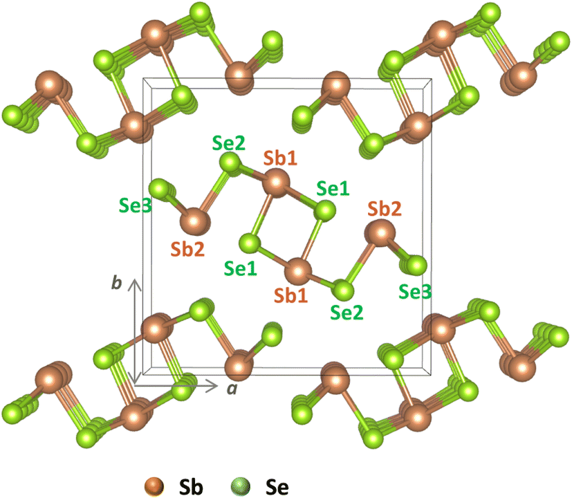 | ||
| Fig. 1 Crystal structure of Sb2Se3 with labeled nonequivalent atomic sites: Sb1 and Sb2 for antimony and Se1, Se2, and Se3 for selenium. | ||
Computational methodology
We performed DFT calculations for antimony selenide with and without dopants using the generalized gradient approximation (GGA) within the framework of the projector-augmented wave (PAW) scheme, as implemented in the Vienna Ab Initio Simulation Package (VASP).39–41 The crystal structure of Sb2Se3 was obtained from experimental data: a = 11.62 Å, b = 11.77 Å, c = 3.962 Å, and α = β = γ = 90°.42 The structure of a 1 × 1 × 3 supercell containing 60 atoms was optimized using the Perdew–Burke–Ernzerhof (PBE) functional with a 4 × 4 × 4 Monkhorst–Pack k-point grid, ensuring convergence of the total energy to less than 10−6 eV per atom and residual force to below 0.01 eV Å−1. The plane-wave cutoff energy was set to 520 eV, and GD3BJ van der Waals corrections43 were applied to account for interactions between Sb2Se3 nanoribbons. The hybrid Heyd–Scuseria–Ernzerhof (HSE) functional,44 incorporating 25% HF exchange, was employed to evaluate total energies, band structures, and density of states (DOS). Band structure calculations used high-symmetry k-points: Γ (0.0, 0.0, 0.0), X (0.5, 0.0, 0.0), Y (0.0, 0.5, 0.0), and Z (0.0, 0.0, 0.5).The defect formation energy of a specific defect α in charge state q, and the charge transition energy level (q/q′), were calculated as:
 | (1) |
 | (2) |
We considered both interstitial and substitutional configurations for potential doping sites. For interstitial defects, five possible configurations were examined within the Sb2Se3 crystal structure. Following structural optimization, the most stable configuration corresponding to the lowest total energy was selected as the thermodynamically favored defect site.
Under equilibrium growth conditions, there are a series of thermodynamic limits on the chemical potential.46 To avoid precipitation of elemental dopant (X) and host elements (Sb and Se), first, their chemical potentials μi should satisfy:
| μi ≤ 0 | (3) |
Second, the host material Sb2Se3 should remain stable, i.e.,
| 2μSb + 3μSe = ΔHf(Sb2Se3) = −1.39 eV | (4) |
Finally, the formation of secondary phases between dopant and host elements should be prevented by satisfying:
| aμX + bμSe < ΔHf(XaSeb) or aμSb + bμX < ΔHf(SbaXb) | (5) |
The formation energies of potential secondary phases were also calculated at the HSE06-GD3DJ level of theory, and the corresponding maximum chemical potential values of dopants under the two growth conditions of Sb2Se3 were determined (see Tables S1 and S2†).
Results and discussion
Undoped Sb2Se3
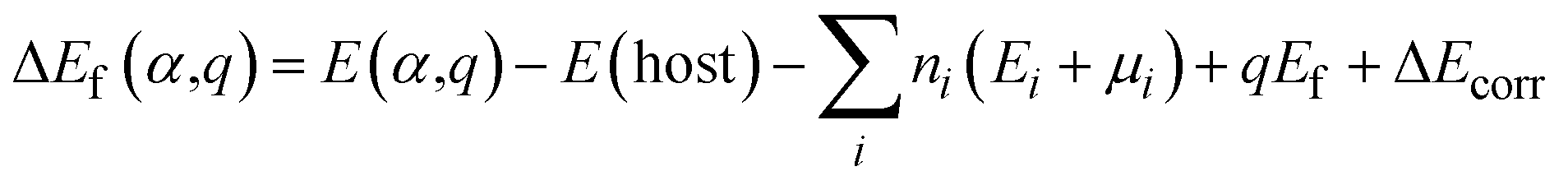
We evaluated the electronic structure of a defect-free Sb2Se3 supercell at the HSE06-GD3DJ level of theory. The calculated band structure (Fig. 2a) reveals that the VBM is located between Γ and X in reciprocal space along the a* axis, while the CBM is positioned between Γ and Z along the c* axis. This results in an indirect bandgap of 1.25 eV, consistent with experimental values of 1.2–1.3 eV.14,47,48 The partial charge densities (Fig. 2b) indicate that the VBM is predominantly localized on Se atoms, while the CBM is distributed across both Sb and Se atoms. Furthermore, the projected DOS (Fig. 2c) shows that the VB primarily originates from selenium orbitals, while the CB exhibits mixed contributions from both antimony and selenium. Overall, these results align well with previous theoretical results.7,9 | ||
| Fig. 2 (a) Band structure, (b) partial charge densities of the CBM (top) and VBM (bottom), and (c) DOS of the Sb2Se3 supercell. In panel (a), the red and blue lines represent the VBM and CBM, respectively, with the Fermi level shifted to zero. | ||
Intrinsic defect properties of Sb2Se3 were examined by calculating the formation energies and transition energy levels under Se-rich and Se-poor conditions. Three types of intrinsic defects were considered: vacancies (VSb and VSe), antisites (SeSb and SbSe), and interstitials (Sbi and Sei) at all nonequivalent atomic sites. The Fermi level (Ef) was varied from zero (VBM) to the bandgap value of 1.25 eV (CBM). For each defect, the formation energies in its lowest-energy charge states were plotted with kinks indicating charge transition energy levels (q/q′), which correspond to ionization levels within the bandgap. Our calculation results show that the same defect at different atomic sites can have distinct formation energies and transition energy levels (see Fig. 3 and 4), consistent with previous theoretical studies.7,8,10 Additionally, Table 1 provides a summary of our results for the intrinsic defect properties of Sb2Se3 and compares them with findings from previous theoretical studies.
 | ||
| Fig. 3 Formation energies of intrinsic defects in Sb2Se3 under Se-rich (left) and Se-poor (right) conditions as a function of the Fermi level (Ef). The dashed gray arrow indicates the Fermi level expected in Sb2Se3. | ||
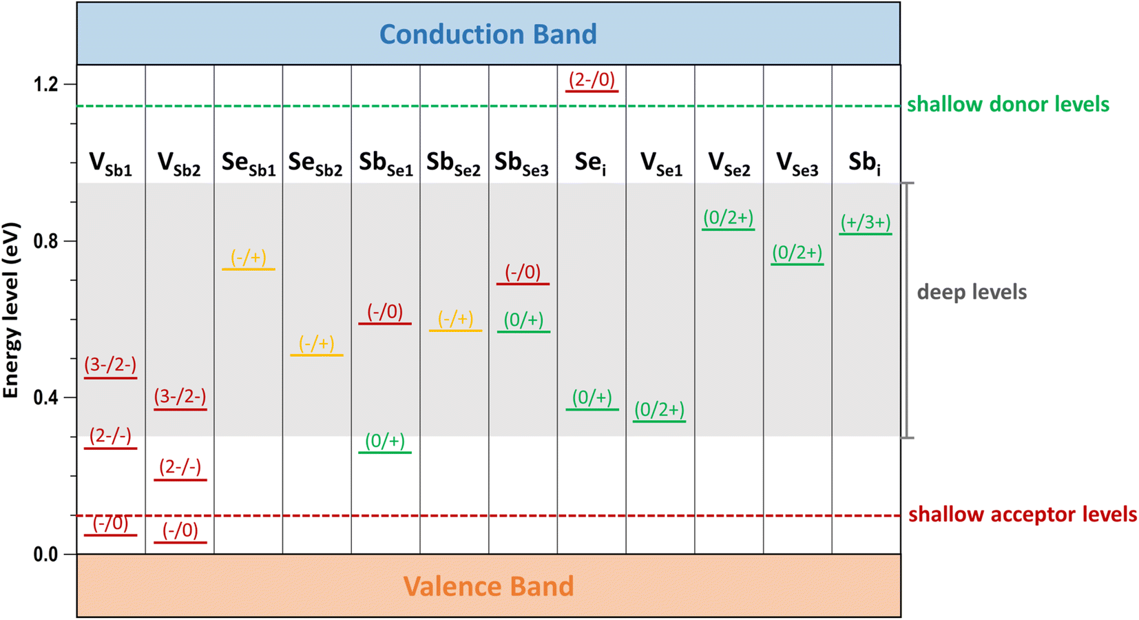 | ||
| Fig. 4 Calculated transition energy levels of intrinsic defects within the bandgap of Sb2Se3. Red, green, and yellow bars represent acceptor, donor, and amphoteric defect levels, respectively. The dashed red and green lines, along with the gray box, indicate ionization levels within the bandgap, distinguishing shallow defect levels from deep defect levels. | ||
| Defect | Defect type | Activation E (eV) | ΔEf (eV) | Ref. | Activation E (eV) | ΔEf (eV) |
|---|---|---|---|---|---|---|
| Se-rich | Our work | Other DFT results | ||||
| SeSb | Amphoteric | SeSb1: VBM + 0.73 | 1.1 | 8 | SeSb1: VBM + 0.70 | ∼1.0 |
| SeSb2: VBM + 0.51 | 1.2 | SeSb2: VBM + 0.62 | ||||
| Acceptor | 7 | SeSb1: VBM + 0.55 | ∼1.0 | |||
| Sei | Neutral | 1.4 | ||||
| VSe | Donor | VSe1: VBM + 0.34 | 1.9 | 7 and 10 | VSe1: VBM + 0.20 | ∼2.0 |
| VSe2: VBM + 0.83 | 2.0 | VSe2: VBM + 0.80 | ||||
| VSe3: VBM + 0.74 | 2.0 | VSe3: VBM + 0.65 | ||||
| 0.5 | ||||||
| Se-poor | Our work | Other DFT results | ||||
| VSe | Donor | VSe1: VBM + 0.34 | 1.4 | |||
| VSe2: VBM + 0.83 | 1.6 | 7 | VSe2: VBM + 0.80 | ∼1.0 | ||
| VSe3: VBM + 0.74 | 1.5 | 8 | VSe3: VBM + 0.81 | ∼1.4 | ||
| SbSe | Donor | SbSe1: VBM + 0.26 | 1.2 | 7 | SbSe1: VBM + 0.18 | ∼1.0 |
| Amphoteric | SbSe2: VBM + 0.57 | 1.0 | 8 | SbSe2: VBM + 0.52 | ∼1.1 | |
| Donor | SbSe3: VBM + 0.57 | 1.1 | ||||
| Sbi | Donor | VBM + 0.82 | <2.0 | 8 | <1.5 | |
As shown in Fig. 3, VSb1 and VSb2 has higher formation energies than other defects, indicating that VSb defects are not easily formed and occur at low concentrations within the lattice. The formation energy of VSb decreases as transitioning from the neutral state to the anionic state, confirming that VSb acts as an acceptor defect. Conversely, VSe behaves as a donor defect, losing electrons as it changes from the neutral state to the doubly positively charged state. The formation energies of VSb and VSe vary with growth conditions, increasing and decreasing, respectively, when the environment shifts from Se-rich to Se-poor conditions.
Antisite defects, such as SbSe and SeSb, are amphoteric, acting as either donor or acceptor defects depending on the position of the Fermi level. This behavior is consistent with previous theoretical findings.8,10 The calculated (−/+) transition energy levels of SeSb1 and SbSe2 are 0.73 eV and 0.51 eV above the VBM, respectively (see Fig. 3 and Table 1). Among the interstitial defects, the anion interstitial defect (Sei) has a lower neutral formation energy than the cation interstitial defect (Sbi). Sei remains electrically neutral across most of Ef range, contributing minimally to conductivity, as it does not significantly alter the charge carrier concentration. In contrast, Sbi acts as a donor defect but has a relatively high formation energy, limiting its concentration.
Low-energy defects result in higher defect concentrations within the material. To ensure that these defects generate free carriers contributing to electrical conductivity, their transition levels should be shallow, i.e., close to either the VBM for acceptor defects or the CBM for donor defects. The calculated transition energy levels of intrinsic defects in Sb2Se3 indicate that most donor and acceptor defects are deep (see Fig. 4). This explains why native antimony selenide exhibits intrinsic-like conductivity behavior. While the (−/0) transition energy level of VSb is shallow, its multiple transition levels suggest that it may act as a recombination centers, detrimental to solar cell performance.
Under Se-rich conditions, the dominant defects appear to be SeSb1 and SeSb2, whereas SbSe2 and SbSe3 are prevalent under Se-poor conditions (see Fig. 3 and Table 1). Note that under thermal equilibrium conditions, Ef is pinned at the intersection of the lowest acceptor and donor formation energies.49 Under Se-rich conditions, the acceptor and donor defects with the lowest formation energies are SeSb2− and SeSb1+, respectively, whereas SbSe1− and Sbi3+ are the acceptor and donor defects with the lowest formation energies under Se-poor conditions, respectively. As a result, the expected Ef positions are 0.54 eV under Se-rich conditions and 0.63 eV under Se-poor conditions (see Fig. 3), which aligns closely with the experimental values of 0.52 eV and 0.60 eV, respectively.50
These results suggest that undoped Sb2Se3 material is intrinsically weakly p-type under Se-rich conditions, whereas it is semi-insulating under Se-poor conditions. Thus, additional treatments, such as doping with alkali or alkaline earth elements, are able to further increase the conductivity and improve the solar cell performance of Sb2Se3. Both interstitial (Xi) and cationic substitutional (XSb) configurations for these dopants were considered (see Fig. 5).
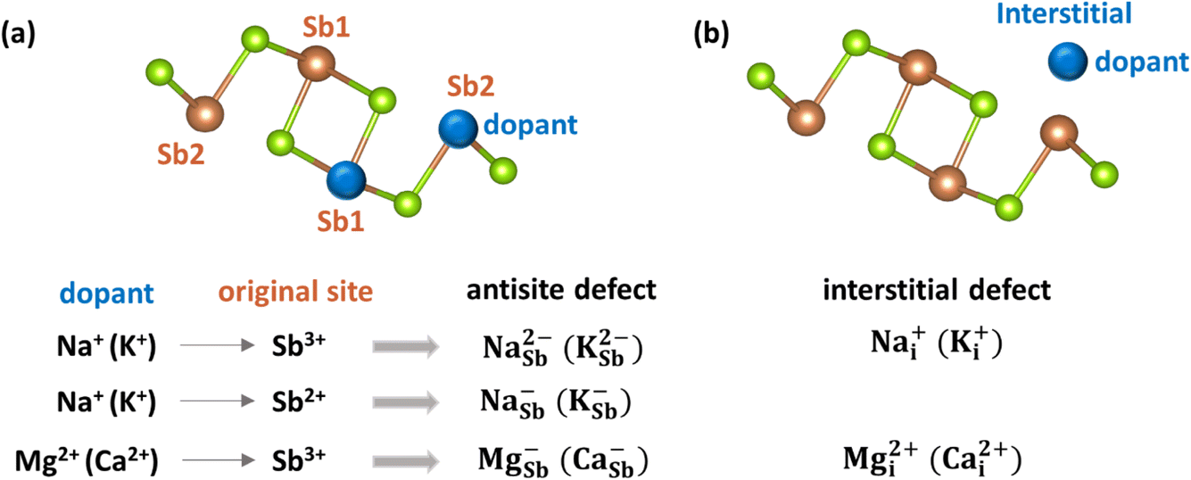 | ||
| Fig. 5 Illustrations of (a) antisite defects and (b) interstitial defects in Sb2Se3. | ||
Sodium doping
The first alkali element investigated in this study is sodium. Sodium in interstitial positions (Nai) acts as a donor defect, donating an electron when it transitions from the neutral state to the singly positively charged state. As a result, the formation energy of Nai decreases as Ef shifts downward toward the VBM (see Fig. 6a). The +1 charged state of Nai is energetically favorable across the entire range of Ef. In contrast, sodium substitution at cationic sites (NaSb) behaves as an acceptor defect, as substitution at Sb sites creates an electronic hole. The formation energy of NaSb decreases as Ef shifts upward toward the CBM. The −2 charged state of NaSb2 is energetically stable for most values of Ef. Notably, NaSb2 has a lower formation energy than NaSb1, indicating that the defect's formation energy depends on the specific atomic site. Overall, the lower formation energy of Nai in the neutral state suggests that sodium preferentially occupies interstitial spaces between Sb2Se3 ribbons, consistent with prior experimental observations.37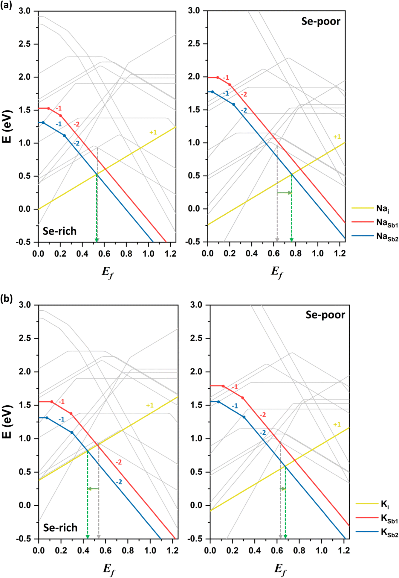 | ||
| Fig. 6 Formation energies of alkali dopants, (a) Na and (b) K, in Sb2Se3 under Se-rich (left) and Se-poor (right) conditions as a function of the Fermi level (Ef) compared with the formation energies of the intrinsic defects represented by gray lines. The dashed gray and green arrows indicate the Fermi levels expected in the undoped and doped systems, respectively. | ||
Under Se-rich conditions, the singly ionized donor defect Nai+ has the lowest formation energy when Ef is less than 0.53 eV, whereas the doubly ionized acceptor defect NaSb22− dominates when Ef is greater than 0.53 eV (see the left side of Fig. 6a). Due to charge neutrality, the Fermi level is pinned near 0.53 eV, aligning closely with the Fermi level (0.54 eV) in undoped Sb2Se3. Thus, sodium doping has a negligible effect on conductivity under Se-rich conditions, leaving the weak p-type conductivity unchanged. These calculation results are consistent with experimental findings,37 which support sodium doping minimally affects conductivity and device performance of Sb2Se3.
Under Se-poor conditions, the (0/+) transition energy level of Nai lies above the CBM, classifying it as a shallow defect. Thus, Nai is easily ionized, contributing to n-type conductivity. The competition between the lowest donor defect Nai+ and the lowest acceptor defect NaSb22− positions Fermi level at approximately 0.76 eV, representing an upward shift of more than 0.1 eV toward the CBM relative to undoped Sb2Se3 (see the right side of Fig. 6a). This upward shift indicates that Na-doped Sb2Se3 under Se-poor conditions exhibits weak n-type conductivity. Moreover, calculated band structure confirms the absence of localized Na-related defect states within the bandgap of Sb2Se3 (see Fig. S1†). Therefore, sodium doping slightly enhances the n-type conductivity under Se-poor conditions.
Potassium doping
The second alkali metal we studied is potassium. The formation energies of K-related defects in K-doped Sb2Se3 are presented in Fig. 6b alongside the formation energies of native defects in the undoped system. Similar to sodium, the doubly ionized acceptor defect KSb22− and singly ionized donor defect Ki+ determine the doping effect of potassium under both Se-rich and Se-poor conditions. However, the impact of the K-doping on electrical conductivity depends on the growth conditions.Under Se-rich conditions, the acceptor defect KSb2 has a lower formation energy than the donor Ki in the neutral state, indicating that potassium doping introduces electronic holes and increases the hole carrier concentration. KSb22− is the most stable defect when Ef is greater than 0.44 eV, while Ki+ is the most stable defect when Ef is below 0.44 eV. This places Ef at 0.44 eV, approximately 0.1 eV closer to the VBM compared with the undoped system. These results suggest that potassium doping enhances p-type conductivity. This finding is in good agreement with the experimental observations, where KOH treatment of Sb2Se3 films increased hole concentrations and shifted the VBM close to Ef.
Under Se-poor conditions, the neutral formation energy of Ki is lower than that of KSb2, meaning that potassium primarily acts as a donor defect by preferentially forming Ki. The (0/+) transition energy level of Ki lies above the CBM, confirming its classification as a shallow defect. Ki produces additional free electrons, influencing n-type conductivity and positioning Ef at 0.67 eV above the VBM. Band structure calculations also reveal that potassium hybridizes well with host material without introducing localized defect levels (see Fig. S1†). Thus, K-doped Sb2Se3 exhibits slight n-type conductivity under Se-poor conditions.
Magnesium doping
Next, we discuss the impact of alkaline earth elements on the conductivity of Sb2Se3. Magnesium is examined as the first alkaline earth atom. The neutral donor defect Mgi has a significantly higher formation energy than the acceptor defects MgSb1 and MgSb2 under both Se-rich and Se-poor conditions (see Fig. 7a). This suggests that magnesium more likely substitutes at cationic antimony sites rather than occupying interstitial positions between atomic nanoribbons. Among the acceptor defects, MgSb2 has a lower energy than MgSb1, making it the more stable defect. Mg-related acceptor defects are located below the VBM, generating free hole carriers and potentially enhancing p-type conductivity. Band structure calculations confirm that Mg doping does not introduce defect states within the bandgap (see Fig. S1†), consistent with experimental reports.36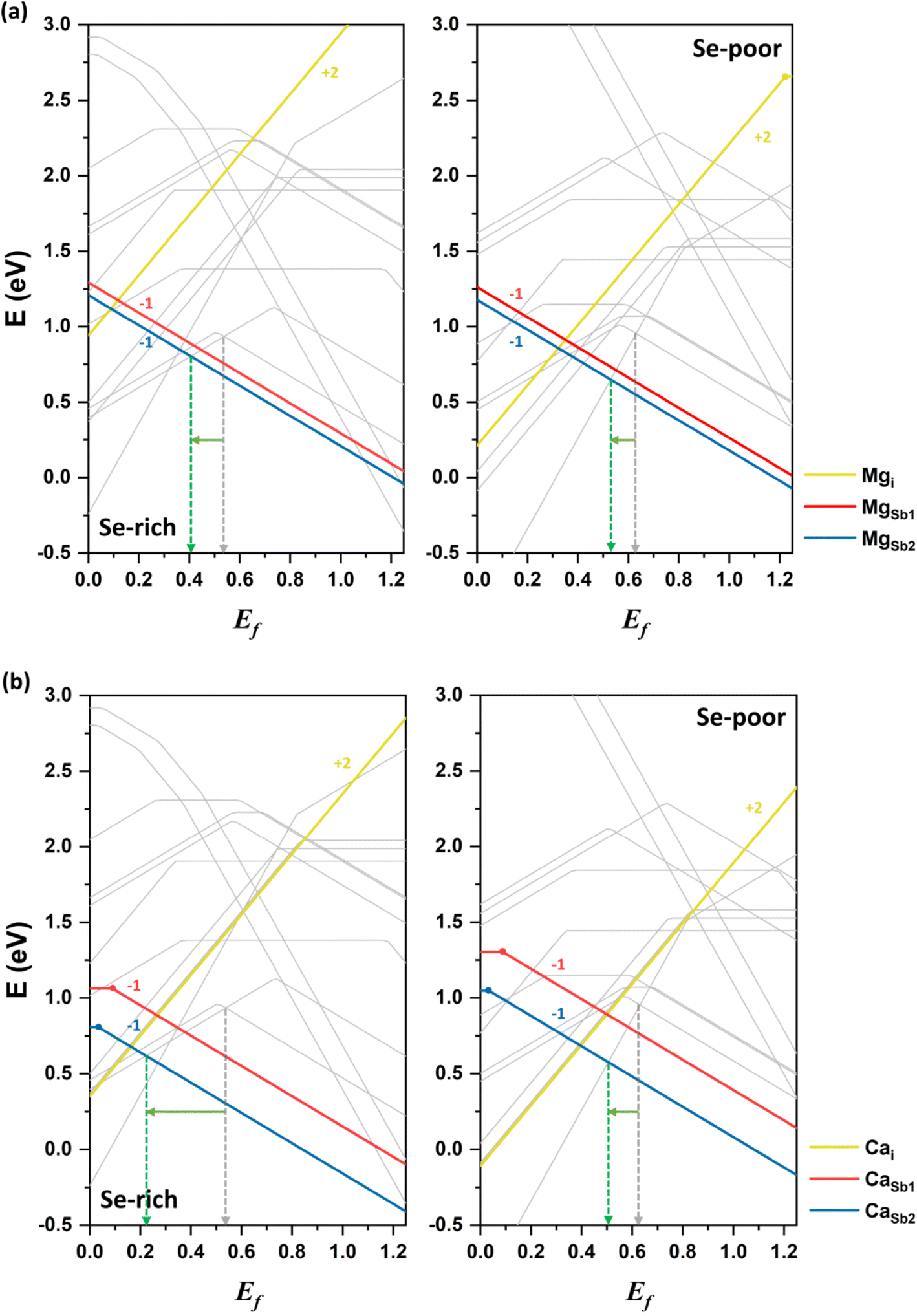 | ||
| Fig. 7 Formation energies of alkaline earth dopants, (a) Mg and (b) Ca, in Sb2Se3 under Se-rich (left) and Se-poor (right) conditions as a function of the Fermi level (Ef) compared with the formation energies of the intrinsic defects represented by gray lines. The dashed gray and green arrows indicate the Fermi levels expected in the undoped and doped systems, respectively. | ||
Experimental data indicates that Mg doping in Sb2Se3 films results in only minor changes in the mobility and device performance, leading to its characterization as an inert dopant.36 However, our calculations show that Mg preferentially forms the acceptor defect MgSb2. Under Se-rich conditions, Ef is positioned at approximately 0.41 eV, while under Se-poor conditions, it lies at 0.53 eV. These values represent a downshift of approximately 0.1 eV compared undoped Sb2Se3 system under both conditions. This shift suggests that Mg doping at Sb sites could enhance p-type conductivity by increasing the free hole concentration, particularly under Se-rich conditions. The discrepancy with experimental results is attributed to the possibility that Mg may not diffuse sufficiently into the active material to substitute for Sb sites. This limited substitution could explain the observed inert behavior of Mg doping in enhancing carrier mobility and device performance. Note that further experimental investigations are warranted to better understand the precise role of Mg doping in Sb2Se3.
Calcium doping
Finally, we consider calcium as the second alkaline earth metal. Given the lack of experimental studies on Ca doping, exploring the effects of calcium treatment of Sb2Se3 via computational approaches is valuable. The formation energy of the acceptor defect CaSb2 is lower than that of the acceptor defect CaSb1, reflecting the characteristic behavior of 1D semiconductor with nonequivalent atom environments (see Fig. 7b). Similar to magnesium, CaSb2 has a much lower formation energy than a donor defect Cai under both Se-rich and Se-poor conditions, indicating that cationic substitution at Sb sites is the dominant doping type for calcium. Consequently, Ca doping is expected to increase the concentration free hole carriers, enhancing the p-type conductivity of Sb2Se3.The Fermi level in Ca-doped system is predicted to be located at approximately 0.22 eV and 0.51 eV under Se-rich and Se-poor conditions, respectively (see Fig. 7b). These positions are determined by the dominance of the acceptor defect CaSb2− under both conditions, while SeSb1+ and Sbi3+ are the lowest-energy donor defects for Se-rich and Se-poor conditions, respectively. Calcium doping downshifts Ef toward the VBM by approximately 0.3 eV under Se-rich conditions and 0.1 eV under Se-poor conditions, supporting an increase in p-type conductivity. Moreover, the (−/0) transition energy levels for CaSb are shallow, with values of 0.09 eV and 0.03 eV for CaSb1 and CaSb2, respectively (see Fig. 8). These shallow transition levels indicate that CaSb defects are easily ionized, promoting a higher concentration of free hole carriers while reducing carrier recombination rates. Overall, our calculations identify calcium as a highly promising p-type dopant for Sb2Se3.
 | ||
| Fig. 8 Calculated transition energy levels of alkali and alkaline earth dopants at different atomic sites within the bandgap of Sb2Se3. The red and green bars represent acceptor and donor defect levels, respectively. The dashed red and green lines, along with the gray box, indicate ionization levels within the bandgap, distinguishing shallow defects from deep defects. The MgSb1 (−/0) and MgSb2 (−/0) levels are shallow acceptor states in the VB, whereas Nai (0/+), Ki (0/+), and Cai (0/2+) are shallow donor states in the CB. | ||
Recent theoretical and experimental studies have proposed lead (Pb) as an effective p-type dopant in Sb2Se3.22,33 For comparison, the formation energy of PbSb2 under Se-rich conditions is 0.7 eV, comparable to that of CaSb2 (0.8 eV). Both defects have lower formation energies than the intrinsic defects in Sb2Se3, making them likely to form. As a result, Ca potentially passivates the deep-level defects in Sb2Se3 that are detrimental to device performance. In addition, the (−/0) transition energy level of PbSb2 under Se-rich conditions (0.15 eV) is deeper than that of CaSb2 (0.03 eV). The lower formation energy of the CaSb2 suggests a higher concentration of free carriers, and its shallower defect level promotes ionization and reduces recombination of free carriers. The band structure of the Ca-doped system shows no Ca-related defect levels within the bandgap; instead, defect states are hybridized with the VB and CB of the bulk material (see Fig. S1†). These findings highlight the effectiveness of Ca doping in enhancing the p-type conductivity of Sb2Se3.
The transition energy levels of alkali and alkaline earth dopants within the bandgap of Sb2Se3 are shown in Fig. 8. Compared with intrinsic defects, these dopants produce shallow donor defects (Nai, Ki, Mgi, and Cai) and shallow acceptor defects (MgSb and CaSb), although NaSb and KSb exhibit relatively deep levels. These results demonstrate that alkali and alkaline earth metal doping can introduce shallow, low-energy defects into Sb2Se3, thereby increasing the concentration of free carriers. Furthermore, band structures calculations confirm that these dopants do not introduce localized defect states within the bandgap (see Fig. S1†). This feature ensures easier ionization of these dopants, contributing positively to the electrical conductivity of Sb2Se3.
Finally, we summarize the defect properties of doped Sb2Se3 systems in comparison to those of the undoped material (see Table 2). Notably, under Se-rich conditions, systems doped with alkaline earth metals exhibit enhanced p-type conductivity compared with the undoped system. This improvement is primarily attributed to the presence of shallow, low-energy, and hole-generating acceptor defects, such as MgSb2 and CaSb2. Experimental investigations of calcium and magnesium doping in Sb2Se3 by our research team are currently underway.
| Se-rich | Sb2Se3 | Na–SbSe2 | K–Sb2Se3 | Mg–Sb2Se3 | Ca–Sb2Se3 |
|---|---|---|---|---|---|
| Conductivity | p-Type | p-Type | p-Type | p-Type | p-Type |
| Ef expected (eV) | 0.54 | 0.53 | 0.44 | 0.41 | 0.22 |
| Hole-generating acceptors | SeSb2− | NaSb22− | KSb22− | MgSb2− | CaSb2− |
| High-population deep donors | VSe22+, SeSb1+ | VSe22+, SeSb1+ | VSe22+, SeSb1+ | VSe22+, SeSb1+ | VSe22+, SeSb1+ |
Conclusions
Using hybrid DFT calculations, we investigated the impacts of alkali and alkaline earth elements on the electronic structure and defect properties of Sb2Se3. In line with recent experimental and theoretical studies,10,50 our calculations confirm that the expected Fermi level for undoped Sb2Se3 are 0.52 eV and 0.63 eV under Se-rich and Se-poor conditions, respectively. These values indicate that the undoped Sb2Se3 has weak p-type conductivity under Se-rich conditions and semi-insulating behavior under Se-poor conditions, with a calculated indirect bandgap of 1.25 eV. The dominant intrinsic defects are SeSb1 and SeSb2 under Se-rich conditions and SbSe2 and SbSe3 under Se-poor conditions.Our findings demonstrate that alkali (Na and K) and alkaline earth (Mg and Ca) elements introduce shallow defects in Sb2Se3 without creating harmful localized defect states within the bandgap. Sodium preferentially occupies interstitial positions, behaving as a donor defect. This enhances n-type conductivity under Se-poor conditions but has minimal effects under Se-rich conditions. Potassium doping varies with crystal growth conditions. K acts as an acceptor dopant by forming KSb2 under Se-rich conditions, while under Se-poor conditions, it behaves as a donor dopant by forming Ki.
Alkaline earth atoms Mg and Ca preferentially substitute at Sb sites, forming acceptor defects that significantly increase hole conductivity. Calcium, in particular, has the lowest formation energy and shallow (−/0) transition levels, comparable to those of Pb, a recently proposed p-type dopant. These results suggest that calcium, as a nontoxic and eco-friendly alternative, could be a potential p-type dopant that enhance hole carrier concentration in Sb2Se3.
Our comprehensive theoretical study provides valuable insights into the intrinsic and extrinsic defect properties of Sb2Se3 and highlights the role of alkali and alkaline earth metal doping in improving its conductivity and solar cell performance. Furthermore, the findings offer broader implications for understanding material properties of Sb2Se3 in applications beyond photovoltaics, including electrochemical cells and photocatalysis.
Data availability
The data supporting this article have been included as part of the ESI.†Conflicts of interest
The authors declare that they have no conflicts of interest.Acknowledgements
This research is supported by the Ministry of Trade, Industry and Energy (MOTIE) and the Korea Institute for Advancement of Technology (KIAT) through the International Cooperative R&D program (Project No. P0024567) and by the DGIST R&D Program of the Ministry of Science and ICT of Korea (25-ET-01). The authors are thankful for the use of the High-Performance Computing (HPC) clusters of the Supercomputing AI Education and Research Center at DGIST.References
- A. Mavlonov, T. Razykov, F. Raziq, J. Gan, J. Chantana, Y. Kawano, T. Nishimura, H. Wei, A. Zakutayev and T. Minemoto, et al., A Review of Sb2se3 Photovoltaic Absorber Materials and Thin-Film Solar Cells, Sol. Energy, 2020, 201, 227–246 CrossRef CAS.
- C. Chen, K. Li and J. Tang, Ten Years of Sb2se3 Thin Film Solar Cells, Sol. RRL, 2022, 6, 2200094 CrossRef CAS.
- A. Bosio, G. Foti, S. Pasini and D. Spoltore, A Review on the Fundamental Properties of Sb2se3-Based Thin Film Solar Cells, Energies, 2023, 16, 1682 CrossRef.
- Y. Wang, S. Ji and B. Shin, Interface Engineering of Antimony Selenide Solar Cells: A Review on the Optimization of Energy Band Alignments, JPhys Energy, 2022, 4, 044002 CrossRef CAS.
- Y. Zhou, L. Wang, S. Chen, S. Qin, X. Liu, J. Chen, D.-J. Xue, M. Luo, Y. Cao and Y. Cheng, et al., Thin-Film Sb2se3 Photovoltaics with Oriented One-Dimensional Ribbons and Benign Grain Boundaries, Nat. Photonics, 2015, 9, 409–415 CrossRef CAS.
- X. Liu, X. Xiao, Y. Yang, D.-J. Xue, D.-B. Li, C. Chen, S. Lu, L. Gao, Y. He and M. C. Beard, et al., Enhanced Sb2se3 Solar Cell Performance through Theory-Guided Defect Control, Prog. Photovolt.: Res. Appl., 2017, 25, 861–870 CrossRef CAS.
- M. Huang, P. Xu, D. Han, J. Tang and S. Chen, Complicated and Unconventional Defect Properties of the Quasi-One-Dimensional Photovoltaic Semiconductor Sb2se3, ACS Appl. Mater. Interfaces, 2019, 11, 15564–15572 CrossRef CAS PubMed.
- C. N. Savory and D. O. Scanlon, The Complex Defect Chemistry of Antimony Selenide, J. Mater. Chem. A, 2019, 7, 10739–10744 RSC.
- A. Stoliaroff, A. Lecomte, O. Rubel, S. Jobic, X. Zhang, C. Latouche and X. Rocquefelte, Deciphering the Role of Key Defects in Sb2se3, a Promising Candidate for Chalcogenide-Based Solar Cells, ACS Appl. Energy Mater., 2020, 3, 2496–2509 CrossRef CAS.
- M. Huang, Z. Cai, S. Wang, X.-G. Gong, S.-H. Wei and S. Chen, More Se Vacancies in Sb2se3 under Se-Rich Conditions: An Abnormal Behavior Induced by Defect-Correlation in Compensated Compound Semiconductors, Small, 2021, 17, 2102429 CrossRef CAS PubMed.
- U. Wijesinghe, G. Longo and O. S. Hutter, Defect Engineering in Antimony Selenide Thin Film Solar Cells, Energy Adv., 2023, 2, 12–33 RSC.
- G. Chen, J. Zhao, S. Chen, Z. Zheng, Z. Su, J. Luo and G. Liang, Perspective of Environmentally Friendly Antimony Selenide-Based Solar Cell, Appl. Phys. Lett., 2024, 125, 20774 Search PubMed.
- K. Zeng, D.-J. Xue and J. Tang, Antimony Selenide Thin-Film Solar Cells, Semicond. Sci. Technol., 2016, 31, 063001 CrossRef.
- Z. Duan, X. Liang, Y. Feng, H. Ma, B. Liang, Y. Wang, S. Luo, S. Wang, R. E. I. Schropp and Y. Mai, et al., Sb2se3 Thin-Film Solar Cells Exceeding 10% Power Conversion Efficiency Enabled by Injection Vapor Deposition Technology, Adv. Mater., 2022, 34, 2202969 CrossRef CAS PubMed.
- Y. Zhao, S. Wang, C. Li, B. Che, X. Chen, H. Chen, R. Tang, X. Wang, G. Chen and T. Wang, et al., Regulating Deposition Kinetics Via a Novel Additive-Assisted Chemical Bath Deposition Technology Enables Fabrication of 10.57%-Efficiency Sb2se3 Solar Cells, Energy Environ. Sci., 2022, 15, 5118–5128 RSC.
- A. Shaker, M. S. Salem and K. Deepthi Jayan, Analysis and Design of P-N Homojunction Sb2se3 Solar Cells by Numerical Simulation, Sol. Energy, 2022, 242, 276–286 CrossRef CAS.
- X. Wang, S. R. Kavanagh, D. O. Scanlon and A. Walsh, Upper Efficiency Limit of Sb2se3 Solar Cells, Joule, 2024, 8, 2105–2122 CrossRef CAS.
- R. M. Martin, Electronic Structure: Basic Theory and Practical Methods, Cambridge university press, 2020 Search PubMed.
- H. M. Ghaithan, Z. A. Alahmed, S. M. H. Qaid and A. S. Aldwayyan, Density Functional Theory Analysis of Structural, Electronic, and Optical Properties of Mixed-Halide Orthorhombic Inorganic Perovskites, ACS Omega, 2021, 6, 30752–30761 CrossRef CAS PubMed.
- A. Shigemi, T. Maeda and T. Wada, First-Principles Calculation of Cu2sns3 and Related Compounds, Phys. Status Solidi B, 2015, 252, 1230–1234 CrossRef CAS.
- D. Yang, W. Ming, H. Shi, L. Zhang and M.-H. Du, Fast Diffusion of Native Defects and Impurities in Perovskite Solar Cell Material Ch3nh3pbi3, Chem. Mater., 2016, 28, 4349–4357 CrossRef CAS.
- M. Huang, S. Lu, K. Li, Y. Lu, C. Chen, J. Tang and S. Chen, P-Type Antimony Selenide Via Lead Doping, Sol. RRL, 2022, 6, 2100730 CrossRef CAS.
- T. D. C. Hobson, H. Shiel, C. N. Savory, J. E. N. Swallow, L. A. H. Jones, T. J. Featherstone, M. J. Smiles, P. K. Thakur, T.-L. Lee and B. Das, et al., P-Type Conductivity in Sn-Doped Sb2se3, JPhys Energy, 2022, 4, 045006 CrossRef CAS.
- K.-J. Yang, S. Kim, S.-Y. Kim, D.-H. Son, J. Lee, Y.-I. Kim, S.-J. Sung, D.-H. Kim, T. Enkhbat and J. Kim, et al., Sodium Effects on the Diffusion, Phase, and Defect Characteristics of Kesterite Solar Cells and Flexible Cu2znsn(S,Se)4 with Greater Than 11% Efficiency, Adv. Funct. Mater., 2021, 31, 2102238 CrossRef CAS.
- H. Xu, R. Meng, X. Xu, Y. Liu, Y. Sun and Y. Zhang, 11.88% Efficient Flexible Ag-Free Cztsse Solar Cell: Spontaneously Tailoring the Alkali Metal Level, Small, 2024, 2408122 CrossRef CAS PubMed.
- Y. Wang, S. Lv and Z. Li, Review on Incorporation of Alkali Elements and Their Effects in Cu(in,Ga)Se2 Solar Cells, J. Mater. Sci. Technol., 2022, 96, 179–189 CrossRef CAS.
- X. Shao, S. Shi, B. Liang, L. Chen, T. Qi, X. Yuan, S. Yu, W. Tang, C. Yang and W. Li, Alkali Metal Pretreatment for Precise Na Doping and Voc Improvement in Cigs Thin-Film Solar Cells, ACS Appl. Mater. Interfaces, 2024, 16, 30147–30156 CrossRef CAS PubMed.
- A. Karami, M. Morawski, H. Kempa, R. Scheer and O. Cojocaru-Mirédin, Sodium in Cu(in, Ga)Se2 Solar Cells: To Be or Not to Be Beneficial, Sol. RRL, 2024, 8, 2300544 CrossRef CAS.
- J. Chen, H. Shen, Z. Zhai, Y. Li, Y. Yi, Y. Lin, C. Yu and Z. Gu, Engineered Cu(Inga)Se2 Thin Films through Caf2 Post-Deposition Treatment for Enhancing Solar Cell Performance, J. Alloys Compd., 2018, 766, 1046–1053 CrossRef CAS.
- J. Chen, H. Shen, Z. Zhai, Y. Li and M. Wang, Effect of Calcium Incorporation on Properties of Cu(Inga)Se2 Thin Film and Solar Cell, Mater. Res. Express, 2019, 6, 096430 CrossRef CAS.
- W.-J. Lee, D.-H. Cho, M. E. Kim, K. Jeong, T.-H. Hwang, W.-J. Kim and Y.-D. Chung, Metastable Defect Curing by Alkaline Earth Metal in Chalcogenide Thin-Film Solar Cells, Appl. Surf. Sci. Adv., 2024, 19, 100539 CrossRef.
- C. F. Cruz-Garcia, J. Rickards, M. A. Garcia, L. R. de la Vega, J. Cañetas-Ortega, J. G. Morales-Morales and L. Rodríguez-Fernández, Surface Morphology and Topography Evolution of Soda-Lime Silica Glass after 1.0 Mev Si Ion Bombardment, Phys. Scr., 2023, 98, 105956 CrossRef CAS.
- W.-H. Li, M. Li, Y.-J. Hu, C.-H. Cheng, Z.-M. Kan, D. Yu, J. Leng, S. Jin and S. Cong, Enhanced Performance of Antimony Selenide Thin Film Solar Cell Using Pbi2 as a Dopant, Appl. Phys. Lett., 2021, 118, 093903 CrossRef CAS.
- G. Chen, X. Li, M. Abbas, C. Fu, Z. Su, R. Tang, S. Chen, P. Fan and G. Liang, Tellurium Doping Inducing Defect Passivation for Highly Effective Antimony Selenide Thin Film Solar Cell, Nanomaterials, 2023, 13, 1240 CrossRef CAS PubMed.
- G. Spaggiari, D. Bersani, D. Calestani, E. Gilioli, E. Gombia, F. Mezzadri, M. Casappa, F. Pattini, G. Trevisi and S. Rampino, Exploring Cu-Doping for Performance Improvement in Sb2se3 Photovoltaic Solar Cells, Int. J. Mol. Sci., 2022, 23, 15529 CrossRef CAS PubMed.
- Y. Li, Y. Zhou, Y. Zhu, C. Chen, J. Luo, J. Ma, B. Yang, X. Wang, Z. Xia and J. Tang, Characterization of Mg and Fe Doped Sb2se3 Thin Films for Photovoltaic Application, Appl. Phys. Lett., 2016, 109, 232104 CrossRef.
- Y. Li, Y. Zhou, J. Luo, W. Chen, B. Yang, X. Wen, S. Lu, C. Chen, K. Zeng and H. Song, et al., The Effect of Sodium on Antimony Selenide Thin Film Solar Cells, RSC Adv., 2016, 6, 87288–87293 RSC.
- H. Guo, C. Zhao, Y. Xing, H. Tian, D. Yan, S. Zhang, X. Jia, J. Qiu, N. Yuan and J. Ding, High-Efficiency Sb2se3 Solar Cells Modified by Potassium Hydroxide, J. Phys. Chem. Lett., 2021, 12, 12352–12359 CrossRef CAS PubMed.
- G. Kresse and J. Furthmüller, Efficiency of Ab-Initio Total Energy Calculations for Metals and Semiconductors Using a Plane-Wave Basis Set, Comput. Mater. Sci., 1996, 6, 15–50 CrossRef CAS.
- J. P. Perdew, K. Burke and M. Ernzerhof, Generalized Gradient Approximation Made Simple, Phys. Rev. Lett., 1996, 77, 3865–3868 CrossRef CAS PubMed.
- J. P. Perdew, K. Burke and M. Ernzerhof, Generalized Gradient Approximation Made Simple [Phys. Rev. Lett. 77, 3865 (1996)], Phys. Rev. Lett., 1997, 78, 1396 CrossRef CAS.
- N. W. Tideswell, F. H. Kruse and J. D. McCullough, The Crystal Structure of Antimony Selenide, Sb2se3, Acta Crystallogr., 1957, 10, 99–102 CrossRef CAS.
- S. Grimme, S. Ehrlich and L. Goerigk, Effect of the Damping Function in Dispersion Corrected Density Functional Theory, J. Comput. Chem., 2011, 32, 1456–1465 CrossRef CAS PubMed.
- J. Heyd, G. E. Scuseria and M. Ernzerhof, Hybrid Functionals Based on a Screened Coulomb Potential, J. Chem. Phys., 2003, 118, 8207–8215 CrossRef CAS.
- C. Freysoldt, J. Neugebauer and C. G. Van de Walle, Fully Ab Initio Finite-Size Corrections for Charged-Defect Supercell Calculations, Phys. Rev. Lett., 2009, 102, 016402 CrossRef PubMed.
- S.-H. Wei, Overcoming the Doping Bottleneck in Semiconductors, Comput. Mater. Sci., 2004, 30, 337–348 CrossRef CAS.
- Z. Li, X. Liang, G. Li, H. Liu, H. Zhang, J. Guo, J. Chen, K. Shen, X. San and W. Yu, et al., 9.2%-Efficient Core-Shell Structured Antimony Selenide Nanorod Array Solar Cells, Nat. Commun., 2019, 10, 125 CrossRef PubMed.
- R. Tang, S. Chen, Z.-H. Zheng, Z.-H. Su, J.-T. Luo, P. Fan, X.-H. Zhang, J. Tang and G.-X. Liang, Heterojunction Annealing Enabling Record Open-Circuit Voltage in Antimony Triselenide Solar Cells, Adv. Mater., 2022, 34, 2109078 CrossRef CAS PubMed.
- J.-H. Yang, W.-J. Yin, J.-S. Park and S.-H. Wei, Self-Regulation of Charged Defect Compensation and Formation Energy Pinning in Semiconductors, Sci. Rep., 2015, 5, 16977 CrossRef CAS PubMed.
- C. Ma, H. Guo, X. Wang, Z. Chen, Q. Cang, X. Jia, Y. Li, N. Yuan and J. Ding, Fabrication of Sb2se3 Thin Film Solar Cells by Co-Sputtering of Sb2se3 and Se Targets, Sol. Energy, 2019, 193, 275–282 CrossRef CAS.
Footnote |
| † Electronic supplementary information (ESI) available. See DOI: https://doi.org/10.1039/d4ta08978b |
| This journal is © The Royal Society of Chemistry 2025 |