
 Open Access Article
 This Open Access Article is licensed under a
 Creative Commons Attribution 3.0 Unported Licence
A wireless, battery-free temperature sensor utilizing the morphotropic phase boundary of HfxZr1−xO2 thin film†
Ketong Yang,
Seungyeob Kim,
Taeseung Jung and
Sanghun Jeon *
*
School of Electrical Engineering, Korea Advanced Institute of Science and Technology, 291 Daehak-ro, Yuseong-gu, Daejeon 34141, Korea. E-mail: jeonsh@kaist.ac.kr
First published on 21st March 2025
Abstract
The development of efficient and self-sustaining wireless sensors plays a crucial role in various applications. Temperature is an essential parameter within wireless sensor networks. It is vital for process regulation, ensuring product quality, and preventing equipment malfunctions. Conventional temperature sensors are often insufficient because they require physical contact or rely on batteries for signal transmission. Furthermore, current solutions frequently conflict with traditional mass production and miniaturization techniques. This paper introduces a wireless temperature sensor that is compatible with conventional semiconductor technologies and operates without batteries. The sensor accurately measures temperature changes by detecting variations in the dielectric constant of the hafnium zirconium oxide (HZO) morphotropic phase boundary (MPB). Wireless signal transmission utilizes passive inductor-capacitor resonance circuits. The MPB HZO temperature sensor demonstrates a temperature sensitivity of 0.15 °C K−1 over a wide temperature range from 293 K to 373 K. Additionally, it shows a sensitivity of 0.01 MHz K−1 within the frequency range of 29.71 MHz to 30.50 MHz. This sensor achieves a maximum wireless detection distance of 10 mm. Combining wireless and battery-free sensor technology with MPB HZO thin films offers a practical alternative for precise and affordable temperature monitoring. This technology has potential applications across diverse fields.
1. Introduction
Temperature sensing has become increasingly important in recent years, especially in climate change awareness,1 energy efficiency regulation,2,3 health and safety concerns,4,5 smart technologies,6,7 and supply chain management.8 The most common types of wireless sensor systems today need active parts or battery power. These include digital wireless methods that use Bluetooth standards and near-field communication protocols,9,10 as well as analog wireless transmission methods that use amplitude or frequency modulation.11–13 Collins’ 1967 initial proposal of an inductor–capacitor (LC) resonant sensor has garnered interest due to its inherent capability for passive wireless signal transmission.14 The intrinsic properties of an LC resonant sensor mean that it doesn't need an external power system or collection apparatus. This makes system design simpler and increases sensor reliability.15,16 Consequently, LC sensors offer considerable advantages in applications such as rotating parts sensing,17 implantable vital sign monitoring,18–20 and operation within extreme environmental conditions.21 However, the evolution of implantable, wearable, and portable devices, alongside the burgeoning Internet of Things, has underscored the demand for compact, highly sensitive LC passive wireless sensors.22–24 Furthermore, elevated production expenses plague conventional component manufacturing methodologies, which frequently rely on organic materials as a temperature-sensitive dielectric layer for capacitors.19,25,26 This reliance on organic materials renders LC sensors incongruent with contemporary advanced manufacturing techniques, thereby impeding the prospects of large-scale mass production.The morphotropic phase boundary (MPB), which refers to the interface between two different crystal phases of ferroelectric polar and tetragonal nonpolar symmetries, has received considerable attention because of the abrupt increase in the dielectric and piezoelectric constants occurring in this region. These properties have garnered considerable attention in various applications, including pressure sensors,27,28 electro-mechanical converters,29,30 and self-powered generators.31,32 The MPBs of zirconium dioxide (ZrO2) and hafnium dioxide (HfO2) have received significant interest in recent years because they are highly compatible with traditional complementary metal–oxide–semiconductor (CMOS) processes and can be easily deposited using atomic layer deposition (ALD) techniques.33–35 However, so far, the application and the demonstration of fluorite-structure MPBs has been limited to mostly CMOS gate insulator36–38 and DARM device39–42 applications, because high capacitance levels are observed when they are close to having no electric field.40,43,44
This study demonstrates the novel application of modern manufacturing techniques and inventive structural design to create a temperature sensor using a 6 nm HZO MPB. The sensor is equipped with a wireless passive LC construction, enabling it to operate effectively in many settings, including at human body temperature, at room temperature, and in aquatic environments. This enhances the longevity and reliability of the sensor. The capacitance value of the 6 nm HZO MPB sensor is measured to be 674.41 pF, and it exhibits a significant temperature sensitivity of 0.15 °C K−1. This article provides a detailed analysis of the temperature sensing mechanism of HZO, utilizing the oxygen vacancy concept. This study provides valuable insights into the mechanism of temperature sensing in HZO by conducting a careful comparison of the temperature sensitivity of various thicknesses of HZO MPB and different phases of 6 nm HZO. The HZO MPB temperature sensor exhibits several outstanding characteristics, including its ability to be produced in large quantities, its high level of sensitivity and reliability, and its capability for wifi passive signal transmission. Therefore, it is a very suitable option for monitoring and sensing in challenging conditions in the context of the Internet of Things.
2. Methods
2.1. Fabrication
We developed LC wireless sensor structures in order to examine the sensing properties of the HZO MPB film. At first, aluminum (Al) (500 nm) and TiN (50 nm) bottom electrodes were applied onto a SiO2/Si substrate using metal sputtering. Afterwards, the PE-ALD technique was used to apply a 6 nm MPB HZO layer with a Hf![[thin space (1/6-em)]](https://www.rsc.org/images/entities/char_2009.gif) :Zr ratio of 1:2. The upper electrode's capacitor area was defined by photolithography and wet etching, specifically using a solution of NH4OH:H2O2:H2O in a ratio of 1:2:5 at a temperature of 37 °C. The HZO film was crystallized by subjecting it to post-metallization annealing using rapid thermal annealing (RTA) at a temperature of 550 °C in a nitrogen atmosphere for a duration of 10 seconds. Furthermore, a 300 nm SiO2 protective layer was applied by chemical vapor deposition. Finally, the metal sputtering technique was used to form an Al inductor layer.
:Zr ratio of 1:2. The upper electrode's capacitor area was defined by photolithography and wet etching, specifically using a solution of NH4OH:H2O2:H2O in a ratio of 1:2:5 at a temperature of 37 °C. The HZO film was crystallized by subjecting it to post-metallization annealing using rapid thermal annealing (RTA) at a temperature of 550 °C in a nitrogen atmosphere for a duration of 10 seconds. Furthermore, a 300 nm SiO2 protective layer was applied by chemical vapor deposition. Finally, the metal sputtering technique was used to form an Al inductor layer.
2.2. Material analysis
We quantitatively measured the properties of the HZO thin film using an X-ray photoelectron spectroscopy (XPS) instrument from K-alpha Thermo VG Scientific. We examined the crystal structure and phase ratio of the HZO thin film based on the patterns obtained from grazing incidence X-ray diffraction (GIXRD, Rigaku diffractometer D/MAX-2500).2.3. Electrical analysis
We measured electrical properties, including capacitance–voltage (C–V) and the relative ratio of the polarization change, using a Keithley 4200 semiconductor parameter analyzer. Additionally, we recorded capacitance–electric field (C–V) curves 105 times of 3.5 V at 10 kHz after the wake-up process. A Keysight 8753 network analyzer read the wireless signal at varying temperatures.3. Results and discussion
Fig. 1a and b delineate the sensor's intricate structure as well as the meticulous assembly process, both highlighted by the use of advanced manufacturing methodologies. The sensor itself comprises three integral components: (1) substrate, (2) HZO MPB capacitor, and (3) inductor. The bottom electrode of the HZO MPB capacitor is a bilayer of Al and TiN. We chose this because it conducts electricity more effectively than a single TiN bottom electrode, thereby reducing frequency changes in the system caused by resistance. We meticulously deposited a protective SiO2 layer to shield the delicate HZO material from external pressure. We then etched two vias in this protective layer to establish essential contact between the capacitor and inductor elements. The inductor is an important part of the sensor architecture because it creates an LC loop when it connects to a capacitor. This generates the functional synergy that the sensor requires to work. We can calculate the resonance frequency using formula (1).
 | (1) |
 | ||
| Fig. 1 Fabrication process and basic properties of the HZO temperature sensor. (a) Fabrication process for the LC temperature sensor. (b) Device structure of the LC temperature sensor, (c) equivalent circuit of the LC temperature sensor, (d) flowchart for the signal conversion process and (e) X-ray diffraction pattern of the 6 nm MPB hafnia thin film. (f) XPS O1s spectrum of the hafnia capacitor. | ||
It is easier to do remote sensing when an inductor L (146.2 nH) is magnetically coupled to a readout coil L0 (200.9 nH). This is done by measuring the impedance Z as a function of frequency across L0. The real part of Z typically displays a peak in a graphical representation. After that, finding the sensor's resonance frequency is possible by fitting the measured data points to the functional form derived from the equivalent circuit (shown in Fig. 1c).
 | (2) |
 and the coupling constant K = 4π2M2/R (K = 10.44 at perfect coupling), where M denotes the mutual inductance between L and L0. The parameter K exclusively influences the amplitude of the resonance, without altering its shape, thereby implying that the determination of fs remains resilient against fluctuations in the distance and orientation between the sensor and the coil. In summary, the relationship of signal transport can be delineated as follows: alterations in temperature induce corresponding changes in the HZO MPB capacitance, thereby resulting in variations in sensor impedance. By deducing the readout frequency and identifying the peak frequency associated with specific temperatures, the actual temperature can be accurately recorded (Fig. 1d).
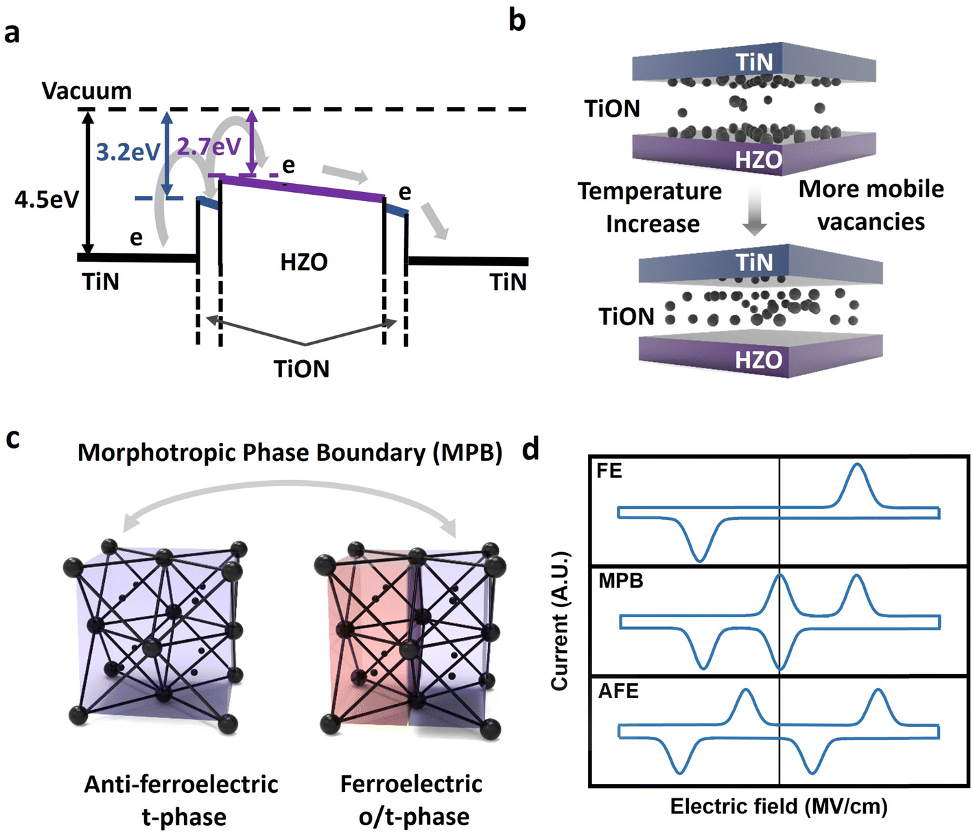
Fig. 1e displays the fundamental X-ray diffraction (XRD) characteristics of MPB HZO. These findings indicate that the material has a significant amount of high relative ferroelectric (orthorhombic; o-phase) phases and anti-ferroelectric (tetragonal; t-phase) phases. The relative content of the o-phase and t-phase in the MPB samples is approximately 1:1, contributing to the high capacitance observed in MPB HZO capacitors. This corresponds to the fact that the o-phase is dominant in FE samples, while the t-phase prevails in AFE samples (Fig. S1, ESI†). The X-ray photoelectron spectroscopy (XPS) investigation reveals the presence of oxygen vacancies at the interface between the TiN electrode and the HZO ferroelectric layer. The presence of oxygen vacancies is the fundamental cause of the temperature dependence found in HZO (Fig. 1f).
The TiON layer predominantly contains oxygen vacancies.45,46 Fig. 2a depicts the energy band diagram of the TiN/HZO/TiN capacitor. The presence of oxygen vacancies in TiON enables the formation of a lower conduction band, thereby facilitating electron transition processes (Fig. S2, ESI†). Fig. 2b shows that as the temperature rises, there are more mobile oxygen vacancies. This makes it easier for vacancies and electronic recombination to happen, which leads to higher switching currents.47 The increased switching current corresponds to the capacitor's augmented charge. Therefore, the switching current positively correlates with capacitance, which quantifies the storage capacity of charge. Consequently, as temperature increases, the capacitance also exhibits an upward trend.
 | ||
| Fig. 2 Mechanism of the HZO temperature sensor. (a) Energy band diagram of the TiN/HZO/TiN capacitor. (b) Schematic diagram of the change of mobile oxygen vacancies with temperature. (c) MPB phase tuning processes, here, represented by concentration. (d) Schematic of FE, MPB, and AFE switching current. | ||
Two primary considerations motivate the selection of MPB HZO as the dielectric layer. First, Fig. 2c shows that the MPB HZO is a mixed crystalline phase that is between the ferroelectric t-phase and the antiferroelectric o-phase in the hafnia material system. This configuration maximizes the dielectric constant (k) in the vicinity of the MPB HZO,44 implying an enhanced capacitance at the MPB in comparison to individual ferroelectric (FE) and antiferroelectric (AFE) films. Additionally, Fig. 2d demonstrates that the MPB HZO sample exhibits the highest switching current near 0 V, unlike the FE and AFE samples. Given the sensor's passive properties that necessitate operation under zero-voltage conditions, we identify the MPB phase as the most suitable option.
There are two methods to achieve MPB HZO: (1) by maintaining a constant film thickness and adjusting the solid solution ratio of ZrO2 in HfO2. For example, in a 6 nm HZO film, increasing the Zr proportion sequentially exhibits FE, MPB, and AFE properties. (2) By maintaining a constant ZrO2 solid solution ratio in HfO2 and varying the film thickness. For instance, in a 1:1 HZO composition, increasing the thickness sequentially reveals AFE, MPB, and FE properties.44 Fig. 3a illustrates the temperature dependence of the capacitance–voltage (C–V) curve for 6 nm FE HZO capacitors. The capacitance value at E+C (0.65 V) increases from 613.61 pF at 297 K to 644.32 pF at 373 K, while the capacitance value at E−C (−1 V) rises from 590.73 pF at 297 K to 614.54 pF at 373 K. Notably, these measurements corroborate the previously explained mechanism, with the rate of change at E+C exhibiting the largest increase of 4.99%. Fig. 3b displays the C–V curve of 6 nm MPB HZO at various temperatures. The capacitance value at EC (0 V) increases from 599.65 pF at 297 K to 675.36 pF at 373 K. Meanwhile, the combined effects of temperature rise and field-induced phase transition led to a transformation of the phase within MPB HZO towards a more stable monoclinic phase at elevated temperatures.40,48 This transformation results in a noticeable change in the shape of the MPB HZO C–V curve. Fig. S3 (ESI†) presents the calculation of the dielectric constant based on capacitance measurements, revealing a linear increase in the dielectric constant with rising temperature. Fig. 3c illustrates the temperature dependence of the C–V curve for 6 nm AFE HZO capacitors. At E+C (0.4 V), the capacitance value increases from 603.63 pF at 297 K to 630.63 pF at 373 K, while at E−C (−0.7 V), it increases from 563.71 pF at 297 K to 589.02 pF at 373 K. At E+C, the percentage increase from room temperature to 373 K is 4.47%, while at E−C, it is 4.49%.
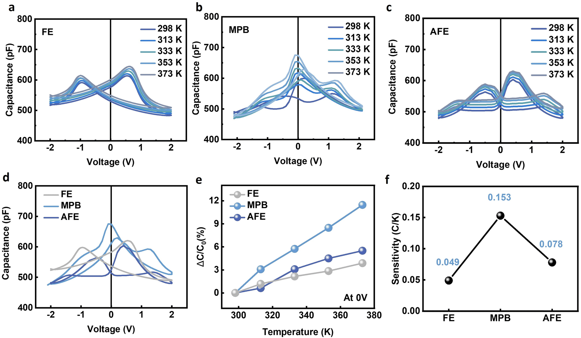 | ||
| Fig. 3 Phase dependency of the HZO temperature sensor. (a) C–V curves of the 6 nm HZO capacitor with different temperatures ((a) 1:1 FE, (b) 1:2 MPB, (c) 1:3 AFE). (d) C–V curves of different phases at room temperature. (e) ΔC/C0 percentage as a function of the temperature for different phase samples. (f) Temperature sensitivity of the different phase samples. | ||
Fig. 3d also shows how the capacitance changes with different Zr ratios in HZO. The MPB composition has the highest capacitance (675.31 pF) at 0 V. This indicates that HZO at the MPB works best for passive devices because its high capacitance value can lessen the effect of resistance in LC circuits. Furthermore, Fig. 3e shows the percentage increase in capacitance versus temperature at 0 V. It shows that MPB HZO capacitors have the highest temperature sensitivity, reaching 0.15 °C K−1 (Fig. 3f). Both FE HZO and AFE HZO also demonstrate a linear increase in capacitance with temperature, albeit with much smaller sensitivities of 0.08 °C K−1 and 0.05 °C K−1, respectively. As a result, MPB HZO capacitors are the most suitable for applications in infinite devices, regardless of passive or high capacitance values.
Fig. 4 presents the capacitance and temperature sensitivity of MPB HZO capacitors with various thicknesses. The C–V curve for 6 nm MPB HZO capacitors changes with temperature, as shown in Fig. 4a. The capacitance values are shown in Fig. 3b. The percentage increase from room temperature to 373 K at EC is 12.63%. Fig. 4b illustrates the temperature dependence of the C–V curve for 10 nm MPB HZO capacitors. The capacitance value at EC increases from 353.33 pF at 297 K to 361.01 pF at 373 K, representing a percentage increase of 2.17%. The 15 nm MPB HZO capacitor, on the other hand, only goes up 1.1% from 297 K to 373 K. Its capacitance value at EC goes up from 191.53 pF at 297 K to 193.39 pF at 373 K (Fig. 4c). Also, the 6 nm MPB HZO capacitors have twice as much capacitance as the 10 nm capacitors and six times as much capacitance as the 15 nm capacitors (Fig. 4d). This means that the resistance has less of an effect on the LC signal output. As shown in Fig. 4e, the EC values of MPB HZO capacitors are approximately 0 V, and the capacitance values change linearly with temperature. The 6 nm MPB HZO capacitor demonstrates the highest temperature sensitivity at 0.15 °C K−1 (Fig. 4f), while the temperature sensitivity of the MPB HZO capacitors is 0.03 °C K−1 at 10 nm and 0.02 °C K−1 at 15 nm. The increase in grain size following the annealing of HZO is responsible for the decrease in capacitance value and temperature sensitivity as the thickness of the HZO film increases. This results in a higher relative proportion of the m-phase in the HZO film, causing the non-ferroelectric phase to dominate.48 Since the non-ferroelectric phase does not have the characteristic of showing high capacitance at EC, the temperature sensitivity is not obvious. Furthermore, because the dead layer at the interface between HZO and TiN remains consistent at approximately 1 nm under the same deposition conditions, there are a large number of oxygen vacancies.49 The proportion of mobile oxygen vacancies in the 6 nm film is relatively high, resulting in increased sensitivity to temperature. This further supports the important role of mobile oxygen vacancies in enhancing the temperature sensitivity of HZO samples.
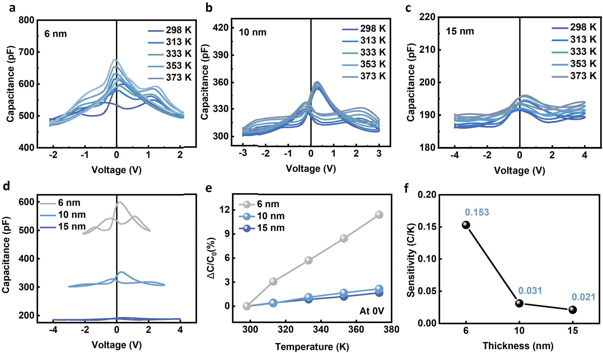 | ||
| Fig. 4 Thickness dependency of the HZO temperature sensor. (a) C–V curves of the MPB HZO capacitor with different temperatures ((a) 6 nm, (b) 10 nm, (c) 15 nm). (d) C–V curves of different thicknesses at room temperature. (e) ΔC/C0 percentage as a function of the temperature for different thickness samples. (f) Temperature sensitivity of the different thickness samples. | ||
Fig. 5 shows the wireless temperature sensor's test results using a network analyzer. Fig. 5a shows the actual test results, which output frequencies of 30.50 MHz, 30.30 MHz, 30.11 MHz, 29.91 MHz, and 29.71 MHz at temperatures of 297 K, 313 K, 333 K, 353 K, and 373 K, respectively. The corresponding output impedances are 7.15 Ω, 7.31 Ω, 7.20 Ω, 6.9 Ω, and 6.71 Ω, with a standard deviation of 0.24 Ω. The experimental output frequencies are slightly lower than the simulation results, a result of signal loss during actual wireless signal transmission.44 Output frequencies at 297 K, 313 K, 333 K, 353 K, and 373 K were simulated and found to be 30.76 MHz, 30.54 MHz, 30.26 MHz, 29.99 MHz, and 29.71 MHz, with output impedances of 6.85 Ω, 6.59 Ω, 6.84 Ω, 6.82 Ω, and 6.92 Ω, and a standard deviation of 0.13 Ω (Fig. 5b). Over 9 fabricated sensors demonstrate a similar dependence of resonance frequency on temperature, validating the design's reliability. Furthermore, Fig. 5c shows the linear decrease in the experimental output frequency with temperature, with a slope of −0.01, compared to the simulation result with a slope of −0.013. The calibration function (T) aligns with simulations, exhibiting minimal temperature hysteresis. As shown in Fig. 5e, the vertical separation distance of LC wireless signal transmission is a critical parameter. We took measurements at distances of 3 mm (Fig. 5f), 6 mm (Fig. 5g), and 10 mm (Fig. 5h). As the measurement distance increases, the output impedance decreases, measured at 6.68 Ω at 3 mm, 2.95 Ω at 6 mm, and 1.77 Ω at 10 mm. The maximum wireless measurement distance is 10 mm, beyond which signals become difficult to detect. Table S1 (ESI†) provides a comparison of key parameters of temperature sensors from previous studies. Factors such as large-scale integration capability using advanced semiconductor manufacturing processes, temperature measurement range, wireless transmission distance, and battery-free operation are evaluated.
 | ||
| Fig. 5 Sensing characteristics of the HZO temperature sensor. (a) Measured shifts of the LC-resonance peak of a sensor as a function of temperature. (c) Measured calibration curves of the change in frequency as a function of temperature. (b) Simulation results for the resonance peaks under conditions similar to those of the experiments in frame. (d) Simulated calibration curves of the change in frequency as a function of temperature. (e) Signal strength as a function of distance in the vertical configuration (x = y = 0). The readout copper ring was placed at (f) 3 mm, (g) 6 mm, and (h) 10 mm vertical distance. | ||
4. Conclusion
This research elucidates the detailed structure and operational principles of a 6 nm MPB temperature sensor, focusing on its constituent components and functionality. The fabrication of the sensor uses advanced manufacturing techniques. The inductor establishes a crucial LC loop with the capacitor, facilitating sensor operation. The resonance frequency calculation and remote sensing mechanism are emphasized, demonstrating the sensor's ability to accurately measure temperature variations. XRD and XPS analyses provide insights into the material properties, particularly the role of oxygen vacancies in influencing temperature dependency. The selection of MPB HZO as the dielectric layer is justified based on its enhanced capacitance and temperature sensitivity. The temperature dependence and capacitance variations of different HZO capacitors confirm the superiority of MPB HZO for passive sensor applications. Additionally, the sensor's performance through simulated and experimental resonance frequency measurements establishes its reliability and operational range. Overall, this study presents a comprehensive overview of the sensor's design, materials, and performance characteristics, highlighting its potential for temperature sensing applications.Author contributions
The manuscript was written through contributions of all authors. All authors have given approval to the final version of the manuscript.Data availability
The data supporting this article have been included as part of the ESI.†Conflicts of interest
There are no conflicts to declare.Acknowledgements
This work was supported by the National Research Foundation of Korea (No. 2021R1A2C2095322).References
- M. R. Miah, M. M. Hasan, J. T. Parisa, M. Alam, F. Akhtar, M. Begum, C. S. Shahriar, A. K. Sayok, F. Abdullah and M. Shamsuddin, World Environment, 2021, 11, 41–82 Search PubMed.
- R. Ruparathna, K. Hewage and R. Sadiq, Renewable Sustainable Energy Rev., 2016, 53, 1032–1045 CrossRef.
- A. Ahmed, A. Azam, Y. Wang, Z. Zhang, N. Li, C. Jia, R. T. Mushtaq, M. Rehman, T. Gueye and M. B. Shahid, Nano Convergence, 2021, 8, 1–42 CrossRef PubMed.
- X. Mu, Z. Wang, M. Guo, X. Zeng and A. J. Mason, “Fabrication of a miniaturized room temperature ionic liquid gas sensor for human health and safety monitoring,” 2012 IEEE Biomedical Circuits and Systems Conference (BioCAS), Hsinchu, Taiwan, 2012, pp. 140–143 DOI:10.1109/BioCAS.2012.6418400.
- W. S. Lee, S. Jeon and S. J. Oh, Nano Convergence, 2019, 6, 1–13 CrossRef PubMed.
- Y. Ma, B. Dong and C. Lee, Nano Convergence, 2020, 7, 12 CrossRef CAS PubMed.
- J. Neto, A. S. Dahiya and R. Dahiya, Nano Convergence, 2025, 12, 2 CrossRef CAS PubMed.
- M. M. Aung and Y. S. Chang, Food Control, 2014, 40, 198–207 CrossRef.
- X. Sun, C. Zhao, H. Li, H. Yu, J. Zhang, H. Qiu, J. Liang, J. Wu, M. Su and Y. Shi, Micromachines, 2022, 13, 784 CrossRef PubMed.
- T. Grosse-Puppendahl, S. Herber, R. Wimmer, F. Englert, S. Beck, J. Von Wilmsdorff, R. Wichert and A. Kuijper, “Capacitive near-field communication for ubiquitous interaction and perception,” Proceedings of the 2014 ACM International Joint Conference on Pervasive and Ubiquitous Computing, 2014, pp. 231–242.
- J. Oetting, IEEE Trans.Commun., 1979, 27, 1752–1762 CrossRef.
- L. Hanzo, W. Webb and T. Keller, Single-and multi-carrier quadrature amplitude modulation: principles and applications for personal communications, WATM and broadcasting, IEEE Press-John Wiley, 2nd edn, 2000 Search PubMed.
- J. F. Sevic, M. B. Steer and A. M. Pavio, International Journal of Microwave and Millimeter-Wave Computer-Aided Engineering: Co-sponsored by the Center for Advanced Manufacturing and Packaging of Microwave, Optical, and Digital Electronics (CAMPmode) at the University of Colorado at Boulder, 1996, vol. 6, pp. 197–216.
- C. C. Collins, IEEE Trans. Biomed. Eng., 1967, 74–83 CAS.
- Q.-A. Huang, L. Dong and L.-F. Wang, J. Microelectromech. Syst., 2016, 25, 822–841 CAS.
- B. Silemek, V. Acikel, C. Oto, A. Alipour, Z. G. Aykut, O. Algin and E. Atalar, Magn. Reson. Med., 2018, 79, 2824–2832 CrossRef PubMed.
- S. Scott, A. Kovacs, L. Gupta, J. Katz, F. Sadeghi and D. Peroulis, “Wireless temperature microsensors integrated on bearings for health monitoring applications,” 2011 IEEE 24th International Conference on Micro Electro Mechanical Systems, Cancun, Mexico, 2011, pp. 660–663.
- V. S. Kumar and C. Krishnamoorthi, Sens. Actuators, A, 2021, 321, 112582 CrossRef.
- D. Lu, Y. Yan, R. Avila, I. Kandela, I. Stepien, M.-H. Seo, W. Bai, Q. Yang, C. Li, C. R. Haney, E. A. Waters, M. R. MacEwan, Y. Huang, W. Z. Ray and J. A. Rogers, Adv. Healthcare Mater., 2020, 9, 2000942 CrossRef CAS PubMed.
- T. J. Harpster, S. Hauvespre, M. R. Dokmeci and K. Najafi, J. Microelectromech. Syst., 2002, 11, 61–67 CrossRef.
- Y. Wang, Y. Jia, Q. Chen and Y. Wang, Sensors, 2008, 8, 7982–7995 CrossRef PubMed.
- N. Wang, N. Zhang and M. Wang, Comput. Electron. Agric., 2006, 50, 1–14 CrossRef.
- M. Masud, P. Vazquez, M. R. Rehman, A. Elahi, W. Wijns and A. Shahzad, IEEE Access, 2023, 95235–95252 Search PubMed.
- G. Asada, et al., “Wireless integrated network sensors: Low power systems on a chip,” Proceedings of the 24th European Solid-State Circuits Conference, The Hague, Netherlands, 1998, pp. 9–16 DOI:10.1109/ESSCIR.1998.186200.
- P.-J. Chen, S. Saati, R. Varma, M. S. Humayun and Y.-C. Tai, J. Microelectromech. Syst., 2010, 19, 721–734 Search PubMed.
- R. I. Rodriguez and Y. Jia, Int. J. Smart Sens. Intell. Syst., 2011, 4, 325–337 Search PubMed.
- Y. Kang, J. Lee, S. Park, J. Kim, S. I. Kim and W. Ryu, ACS Appl. Mater. Interfaces, 2023, 15, 17653–17663 CrossRef CAS PubMed.
- V. N. Thakur, A. Zafer, S. Yadav and A. Kumar, Sens. Actuators, A, 2019, 297, 111536 CrossRef CAS.
- W. D. Dong, P. Finkel, A. Amin and C. S. Lynch, Appl. Phys. Lett., 2012, 100, 042903 CrossRef.
- I. M. McKinley, S. Goljahi, C. S. Lynch and L. Pilon, J. Appl. Phys., 2013, 114, 224111 CrossRef.
- V. Annapureddy, H. Palneedi, G.-T. Hwang, M. Peddigari, D.-Y. Jeong, W.-H. Yoon, K.-H. Kim and J. Ryu, Sustainable Energy Fuels, 2017, 1, 2039–2052 RSC.
- X. Gao, C. Qiu, G. Li, M. Ma, S. Yang, Z. Xu and F. Li, Appl. Energy, 2020, 271, 115193 CrossRef CAS.
- J. Hwang, H. Joh, C. Kim, J. Ahn and S. Jeon, ACS Appl. Mater. Interfaces, 2024, 16, 2467–2476 CrossRef CAS PubMed.
- A. Kashir and H. Hwang, Nanotechnology, 2021, 32, 445706 CrossRef CAS PubMed.
- Z. Zhou, L. Jiao, Z. Zheng, Y. Chen, K. Han, Y. Kang, D. Zhang, X. Wang, Q. Kong and C. Sun, Nano Convergence, 2025, 12, 3 CrossRef CAS PubMed.
- H. Joh, S. Nam, M. Jung, H. Shin, S. H. Cho and S. Jeon, ACS Appl. Mater. Interfaces, 2023, 15, 51339–51349 CrossRef CAS PubMed.
- T. Jung, S. Nam and S. Jeon, IEEE Trans. Electron Devices, 2024 Search PubMed.
- V. Gaddam, G. Kim, T. Kim, M. Jung, C. Kim and S. Jeon, ACS Appl. Mater. Interfaces, 2022, 14, 43463–43473 CrossRef CAS PubMed.
- G. Kim et al., “Design Guidelines of Thermally Stable Hafnia Ferroelectrics for the Fabrication of 3D Memory Devices,” 2022 International Electron Devices Meeting (IEDM), San Francisco, CA, USA, 2022, pp. 5.4.1–5.4.4 DOI:10.1109/IEDM45625.2022.10019458.
- M. Jung, V. Gaddam and S. Jeon, Nano Convergence, 2022, 9, 44 CrossRef CAS PubMed.
- M. Jung, C. Kim, J. Hwang, G. Kim, H. Shin, V. Gaddam and S. Jeon, ACS Appl. Electron. Mater., 2023, 5, 4826–4835 CrossRef CAS.
- D. Das, B. Buyantogtokh, V. Gaddam and S. Jeon, IEEE Trans. Electron Devices, 2021, 69, 103–108 Search PubMed.
- A. Kashir and H. Hwang, Phys. Status Solidi A, 2021, 218, 2000819 CrossRef CAS.
- M. H. Park, Y. H. Lee, H. J. Kim, Y. J. Kim, T. Moon, K. D. Kim, S. D. Hyun and C. S. Hwang, ACS Appl. Mater. Interfaces, 2018, 10, 42666–42673 CrossRef CAS PubMed.
- G. Tian, G. Xu, H. Yin, G. Yan, Z. Zhang, L. Li, X. Sun, J. Chen, Y. Zhang and J. Bi, Adv. Mater. Interfaces, 2022, 9, 2102351 CrossRef CAS.
- S. Lancaster, P. D. Lomenzo, M. Engl, B. Xu, T. Mikolajick, U. Schroeder and S. Slesazeck, Front. Nanotechnol., 2022, 4, 939822 CrossRef.
- M. Pešić, F. P. G. Fengler, L. Larcher, A. Padovani, T. Schenk, E. D. Grimley, X. Sang, J. M. LeBeau, S. Slesazeck and U. Schroeder, Adv. Funct. Mater., 2016, 26, 4601–4612 CrossRef.
- M. H. Park, H. J. Kim, Y. J. Kim, W. Lee, T. Moon and C. S. Hwang, Appl. Phys. Lett., 2013, 102, 072901 CrossRef.
- Y. Kim, D. Kim, J. Kim, Y. Chang, T. Noh, J. Kong, K. Char, Y. Park, S. Bu and J.-G. Yoon, Appl. Phys. Lett., 2005, 86, 102907 CrossRef.
Footnote |
| † Electronic supplementary information (ESI) available. See DOI: https://doi.org/10.1039/d4tc03033h |
| This journal is © The Royal Society of Chemistry 2025 |