
 Open Access Article
 This Open Access Article is licensed under a Creative Commons Attribution-Non Commercial 3.0 Unported Licence
Selective reaction at grain boundaries addressing organic field effect transistor trap states†
Feifei
Li
a,
Matthew C.
Williams
a,
Matthew
Waldrip
 b,
Colin
Tyznik
b,
Tharushi D.
Ambagaspitiya
c,
Derek
Dremann
b,
Katherine Leslee Asetre
Cimatu
c,
Oana D.
Jurchescu
b and
Jacob W.
Ciszek
*a
b,
Colin
Tyznik
b,
Tharushi D.
Ambagaspitiya
c,
Derek
Dremann
b,
Katherine Leslee Asetre
Cimatu
c,
Oana D.
Jurchescu
b and
Jacob W.
Ciszek
*a
aDepartment of Chemistry and Biochemistry, Loyola University Chicago, Chicago, Illinois 60660, USA. E-mail: jciszek@luc.edu
bDepartment of Physics and Center for Functional Materials, Wake Forest University, Winston-Salem, North Carolina 27109, USA
cDepartment of Chemistry and Biochemistry, Ohio University, Athens, OH 45701, USA
First published on 23rd December 2024
Abstract
Trap states generated at grain boundaries often dominate the charge transport behavior of polycrystalline organic field effect transistors (OFETs). While these grain boundaries can be reduced through careful processing, unfortunately they cannot be completely suppressed. In this work, we introduce an approach that renders the grain boundaries inactive. Diels–Alder chemistry, which selectively reacts at the grain boundaries within organic semiconductor thin films, is utilized to attach a dipole-containing molecule in a localized manner. This induced dipole alters the surface potential, shifting the mean energy within the grain boundary and resulting in significantly enhanced device performance. Conductance increases exceed two orders of magnitude with the increase proportional to the amount of grain boundary reacted. In OFETs, this generated a doubling in charge carrier mobility and a reduction in the threshold voltage. The ability to tune the performance and uniformity of fabricated films, regardless of their initial grain size or conductance, represents a significant advance in post-fabrication optimization.
Introduction
Electronic trap states can significantly hamper the properties of optoelectronic devices based on small molecule organic semiconductors.1–5 For example, charge carrier mobility values for polycrystalline films are typically lower by one to three orders of magnitude compared to single crystal measurements.6–9 The need for high mobility in devices (>10 cm2 V−1 s−1 for active-matrix driven organic light-emitting diode/OLED displays) then means the number of potential semiconductors is limited to but a handful of materials.3,10–12 Mobility limitations of polycrystalline films are generally accepted as unavoidable.Intrinsically, the trap states at grain boundaries represent one of the major factors that govern charge transport in polycrystalline small molecule organic semiconductors. The grain interface contains a high degree of structural mismatch/disorder and often the boundaries extend the entire width of the device channel.13,14 The boundary between the grains contains areas where the mean energy is significantly lower (valleys) or higher (barriers),15–17 and the energy difference of these traps is commonly on the order of 100 meV.14,18 The net result is several orders of magnitude larger resistance across grain boundaries compared to the intra-grain resistance, and overall lower conductivity in devices based on these films.14,18 Given the challenges posed by grain boundaries, significant effort has been dedicated to minimizing and even suppressing them. A major focus has been on developing techniques to grow single crystals over large areas.19,20 While eliminating grain boundaries may be a viable option in certain contexts, it is crucial to explore alternative solutions that address the root causes of this challenge.
One solution was first hinted at by He et al., who utilized highly localized chemistry to dope step edges to eliminate trap states:21 rather than focusing on minimizing defect density during film growth, they used chemistry to selectively address the flaws formed by crystallographic defects post-fabrication. This chemistry-based approach has obvious applicability to grain boundaries. Grain boundaries are typically highly reactive,22 and thus, it should be possible to selectively passivate these sites with molecules capable of shifting the mean energy in the grain boundary closer to that of the crystalline domains.6,23 Moreover, by selecting the correct chemistry, there is the potential for these reaction to propagate,22 potentially allowing the passivation to move from the surface lower into the grain boundary. If harnessed correctly, this could nullify, or at least minimize, the impact of the detrimental transport behavior within.24
Herein, we utilize Diels–Alder chemistry22,25,26 to facilitate a reaction along the grain boundaries of pentacene thin films (Fig. 1) which reduces the associated resistivity and results in an overall improvement of the electrical properties of the film. The reactive molecule, maleic anhydride, introduces a dipole at the interface, which shifts the mean energy landscape within the grain boundary to facilitate more efficient charge transport. We show that the effect is controllable, persistent, and related to the chemistry, while the measured improvements in electrical properties scale with the amount of grain boundary present in samples and the change in surface potential induced by the reaction. The impact on the threshold voltage and mobility of the organic field-effect transistors (OFETs) based on these films has also been explored. Our results introduce a powerful solution to tackle the performance bottleneck of grain boundaries in organic devices using postprocessing.
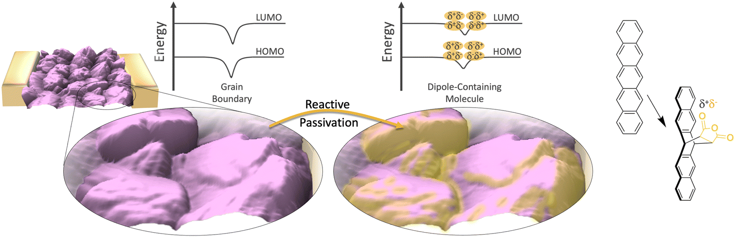 | ||
| Fig. 1 Schematic of the selective passivation of grain boundaries in a pentacene (purple) thin-film device. Reactive passivation is accomplished via the dosing of maleic anhydride, which undergoes a Diels–Alder with the pentacene (far right) at high energy grain boundaries and defects.22 The energy diagram depicts the shift of the mean energy in the grain boundary, which is induced by the molecular dipole appended to the adjoining faces of adjacent grains. | ||
Results and discussion
The majority of vapor-deposited organic semiconductors form ordered films that are polycrystalline.27 Here, organic semiconductors are usually sublimed onto substrates at high temperatures and high vacuum, with a standard nucleation/growth process generating the films.27–29 The resulting thin film contains numerous individual crystal domains. Along these domains, there are domains’ edges, which will form grain boundaries. Grain boundaries are planar defects that are ubiquitous in all polycrystalline materials and are interfaces formed naturally by numerous single-crystalline grains that connect with one another. Though detrimental to device performance, defect sites (especially grain boundaries) can serve as loci for reaction as these locations have less van der Waals stabilization and more exposed reactive groups.30 There have been a handful of reports of organic semiconductors reacting in a spatially controlled manner.21,22,31,32In this study, we perform localized chemical reactions which target the grain boundaries present in vacuum-deposited pentacene thin films and investigate the impact on charge transport. Pentacene was chosen because of extensive precedence for its post-deposition modification via reaction.22,33–35 Thin-film pentacene exposed to volatile adsorbates is known to react in a highly defined manner,25 importantly appending the grain boundaries first before later propagating into the grain.22 The adsorbates themselves are also highly tunable.26,36,37 In this work, an adsorbate containing a molecular dipole was utilized in order to shift the surface potential and mean energy of the boundary (Fig. 1). A secondary reason for choosing pentacene is that its grains can be controllably generated from 0.1 to 20 μm, allowing control over the total grain boundary length for these experiments.22,38 Beyond that, pentacene is also one of the most widely studied organic semiconductors and exhibits mobility, reaching 35 cm2 V−1 s−1 in single crystals and 2 cm2 V−1 s−1 in polycrystalline films.39–41 It also shows good chemical stability, ordered thin film structure, and a good interface with commonly used electrode metals such as gold.42
For accessing the electrical properties, gold electrodes have been defined in a bottom contact configuration. In this geometry, the contacts lie below the organic semiconductor and are unaffected by the surface chemistry, allowing these studies to focus on the pentacene film. The thin-film pentacene was exposed to maleic anhydride vapor following precedent detailed elsewhere,22,26,33,34 with the Diels–Alder reaction occurring for 8–48 h at 37 °C. Our home-built system (Fig. S1, ESI†) allows for the real-time measurement of current while the reaction is occurring in the channel. Fig. 2 shows representative current versus time measurements at constant voltage (plotted as conductance, I/V) for the reaction of maleic anhydride and pentacene. The maleic anhydride (tan line) shows a notable increase in conductance, 20 times greater than before the reaction. The characteristics of the tan line can be described as (1) a nearly linear increase where diffusion of the adsorbate to the sample limits the amount of change and (2) a saturating exponential attributed to easily accessible reaction sites being passivated. The increase is representative of our samples; we have seen increases as large as a factor of 939×, while the median change is 71× for the most common sample type reported here (100 nm thick pentacene thin films deposited onto room temperature substrates, 33 samples).
 | ||
| Fig. 2 (left) Conductance of a pentacene thin film as a function of exposure time to reactive maleic anhydride (tan) or control molecules succinic anhydride (red)/DDF (blue). Data taken at 0.2 V and a film thickness of 200 nm. (right) Associated spectroscopic samples. The top displays the infrared spectra of pentacene (grey), pentacene exposed to maleic anhydride for 12 h (dashed tan), and pentacene exposed for 22 h (solid tan). Regions displayed are associated with carbonyl stretches and ring deformations (1780 and 1260 cm−1 respectively). Atomic displacement vectors for the vibration at 1260 cm−1, are shown in the middle of the spectra. The blue lines highlight the portion of the molecules associated with the two measured vibrations at 1780 and 1260 cm−1. The bottom figure contains UV-vis spectra that quantify the extent of reaction after exposure to maleic anhydride for 42 h at a higher temperature of 50 °C. Inset highlights the small (2.6%) decrease in the S0–S1 absorption band of pentacene. | ||
The measured effects with maleic anhydride are heavily correlated with the extent of reaction. Witness samples were characterized with polarization modulation-infrared reflection–absorption spectroscopy (PM-IRRAS) before and after the maleic anhydride reaction (Fig. 2). Characteristic product peaks at 1780 cm−1, 1260 cm−1, and 930 cm−1 all display the expected increase in intensity for the timescales for these reactions.34 Additionally, device samples were directly examined via UV-vis before and after reaction to estimate the extent of reaction via the decrease in intensity of the Davydov-split S0–S1 absorption bands at 672 nm (Fig. 2).43 The reacted spectrum utilized significant harsher conditions (42 h at 50 °C) than the rest of the reactions reported herein to maximize signal change, and showed a decrease in intensity of ∼2.6%. This difference corresponds to the reaction of the first 4–5 molecular layers of pentacene.44 For the milder conditions herein, 1–3 molecular layers of pentacene are converted, depending on the exposure time. This coverage is sufficient to reach the maximum conductance, while more extensive reaction/harsher conditions result the gradual decrease from this maximum (Fig. S2, ESI†).
To further confirm the effects were due to a reaction, two non-reactive controls were selected and tested. These species have been studied extensively in the context of non-covalent surface physisorption or absorption33 and can be utilized to rule other modes of interactions with the surface. Succinic anhydride (Fig. 2, red) was chosen due to its nearly identical electronic structure to maleic anhydride, except for the double bond necessary for the reaction, though it is notably less volatile.45 5,5-Dimethyl-dihydrofuran-2-one (DDF, Fig. 2, blue) has minor structural differences but is expected to have a higher vapor pressure than that of maleic anhydride (0.30 Torr).45 Similar real-time measurements with the controls show increased conductance occurs only with the reactive maleic anhydride. Of the two controls, succinic anhydride did not show any increase in conductance, instead, there was a decrease in conductance (from 1.7 to 1.1 × 10⁻¹⁰ S). DDF showed a minor increase within the first 2 h (1.8×), and over the entirety of the measurement there is a net decrease. The increase observed with DDF may be due to the preferred alignment of some of the molecules in the initial state, which later randomizes to a non-contributing orientation. These controls provide further evidence that the increase in current for maleic anhydride is due to the covalent bonding upon the Diels–Alder reaction which gives a fixed orientation of the molecular dipole at the surface.
We found a strong correlation between the reaction-based conductance increase and the amount of grain boundary present in the pentacene sample, confirming our hypothesis. Thin films prepared on substrates at room temperature have a significantly smaller grain size (and thus more grain boundary) compared to those prepared on substrates with elevated temperatures (Fig. 3).22,38 In this case, the average grain size changes from 176 ± 37 nm (25 °C) to 287 ± 26 nm (45 °C), while the total grain boundary length decreases from 448 ± 89 μm to 250 ± 10 μm (values for 5 × 5 μm images, Fig. S3, ESI†). Unsurprisingly, the median conductance across pristine samples with the small grains (more grain boundaries) begins significantly worse than that of the larger grains (Fig. 3). What is intriguing is the conductance measured after the reaction. Post-reaction conductivity enhancement is observed in both sample types. However, the magnitude of this increase is significantly lower for samples with larger grains (reduced grain boundary). This observation aligns with the hypothesis that grain boundaries act as dominant trap state locations. Consequently, samples with a lower inherent defect density (larger grains) exhibit a diminished capacity for conductivity improvement. However, it is interesting to note that both samples converge to roughly the same conductance, that is, when grain boundaries are “healed” via reaction, both the larger grain and smaller grain samples end up at roughly the same median value.
 | ||
| Fig. 3 AFM image of pentacene grains grown on substrates at room temperature (top) or substrates at 45 °C (bottom). The scale bar in both images is 500 nm. Conductance before (grey) and after reaction (tan) is indicated to the right of each image. Device data was taken at 5 V. Central marks indicate the median, the boxes the 25th–75th percentile, and the whiskers the 10th percentile to the 90th. Pentacene thickness is 100 nm. | ||
The improvement in conductance appears to show a dependence on the thickness of the thin film. Comparing pentacene thin films that are 100 nm thick to 200 nm (Fig. 4), several aspects stand out. First, there is a slight difference in the initial conductance for the two thicknesses; the median conductance at 100 nm was 7.8 × 10⁻¹⁰vs. 4 × 10⁻⁹ S at 200 nm for these samples. Second, regardless of the initial properties, the thinner films experienced a more drastic improvement. This is especially apparent if the films are grouped by their starting conductivity levels, that is 10−10 S are grouped together as are 10−9, 10−8, and 10−7 (tan boxes, Fig. 4), so that those starting at lower currents become visually apparent. Third, it is remarkable that, regardless of the starting conductivity, all films end up with a similar current level. The median final conductance indicated in Fig. 4 are as follows: 2.7 × 10⁻⁸ S for low initial conductance 100 nm thick films, 2.6 × 10⁻⁸ S for high conductance 100 nm thick films, and 3.3 × 10⁻⁸ S for 200 nm thick films. This result mirrors the trend seen with the grain sizes, confirming the hypothesis that the reaction has the ability to ‘heal’ a device irrespective of its starting conductance level and its thickness. The latter point is worth dwelling on as uniformity is a significant impediment to OFET adoption.46 This same median is seen across multiple experiments and reached regardless of initial thickness or grain size, suggesting the potential to reduce variance stemming from the original pentacene deposition.
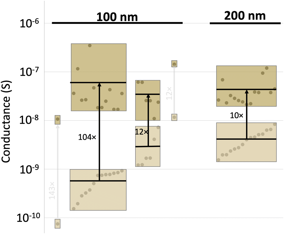 | ||
| Fig. 4 Conductance of pentacene devices containing 100 or 200 nm thick channels before (light tan) and after (dark tan) reaction. To highlight the tendency for devices to finish reactions at similar conductivity levels, individual device measurements (circles) are grouped by starting conductivity levels, with the box indicating the range of values and the black horizontal line indicating the average value. | ||
Mechanistically, we hypothesize that the dipole associated with maleic anhydride is altering the mean energy in the grain boundary, reducing its electrical resistance. The reaction generates a product with the geometry shown in Fig. 5(a) and a component of the separated charge of the dipole is oriented perpendicular to the grain boundary which will lower the energy of pentacene's Fermi level with respect to vacuum (Fig. 5(b)). If, for example, grain boundaries are accurately modeled as double Schottky barriers (or valleys),14,47 then the application of mirrored dipoles on both sides of the grain boundary reduces the energy valley opening up conduction pathways. Measurements supportive of this hypothesis can be seen in Fig. 5(c), where Kelvin probe measurements for pentacene oriented parallel to the surface show a change in the surface potential (or ΔΦ), with timescales similar to that of the conductance change and reaction. Specifically, at 12.5 h, the majority of the surface potential change has already occurred (327 mV), which is in line with the conductance changes and spectroscopy (Fig. 2 and Fig. S2, ESI†). The change in surface potential from maleic anhydride is persistent and the defined orientation of the dipole, which results from the reaction, appears to be the key to this effect. The control molecules (no preferred orientation) show negligible changes in surface potential (−24 mV and −5 mV, for DDF and succinic anhydride, respectively). Controls of untreated pentacene (99 mV and 61 mV, at 12.5 h and 18 h respectively) show only minor shifts. Note that for these measurements, the dipole applied following the reaction is oriented toward the probe (for measurement purposes). In contrast, for the thin-film phase pentacene (oriented upright), the dipole would be oriented towards the grain boundary.
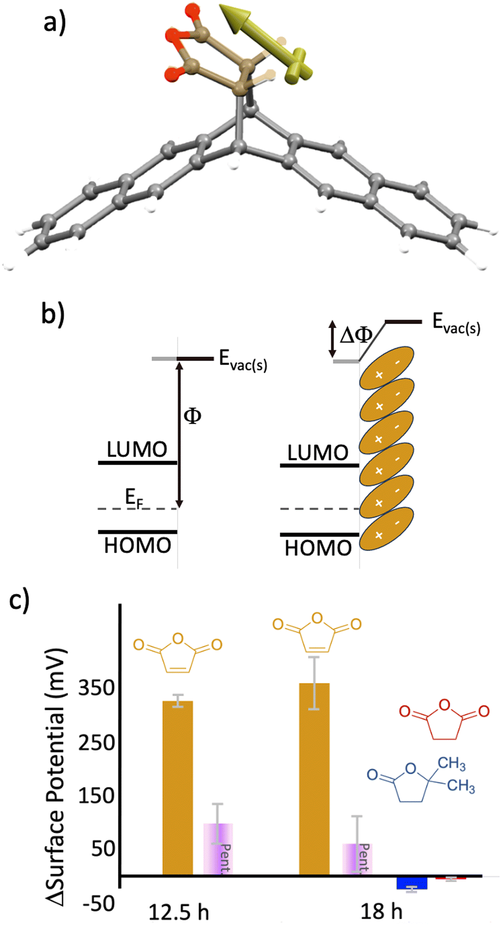 | ||
| Fig. 5 (a) Energy minimized structure of the product formed during the reaction of pentacene and maleic anhydride. The yellow vector indicates the direction of the molecular dipole. Geometry optimization was generated via molecular mechanics using Spartan molecular modeling software. (b) Electronic structure of pentacene indicating the work function Φ (left) and change in work function (ΔΦ) after application of a molecular dipole (right). (c) Relative change in the surface potential for pentacene samples that have been exposed to heat (purple box), maleic anhydride (tan), DDF (blue), and succinic anhydride (red). Error bars represent the standard deviation over the measured samples. Note, that the positive change in surface potential represents an increase in work function (i.e., Fig. 5(b)). | ||
If the results for reacted devices do indeed stem from significantly reduced valleys, there should be commensurate improvements in charge carrier mobility. Accordingly, OFET devices have been fabricated and tested to study these phenomena.48 Top-gate bottom-contacts and bottom-gate, bottom-contacts OFETs with Cytop and SiO2 dielectrics, respectively, have been fabricated on the same films by adopting the structure depicted in Fig. 6(a). By evaluating the charge carrier mobility in the same film, we eliminate the discrepancies originating from sample-to-sample inhomogeneities. This structure also provides independent access to the top and bottom surfaces of the film, allowing us to evaluate if the reactions at the grain boundaries are accruing throughout the thickness of the film, or just in the top few nm. Benchmark samples shown in Fig. 6(b) are of an unreacted pentacene thin film (100 nm) with Cytop dielectric and a top gate.49,50 The extracted device properties agree well with previous reports and show an average mobility of 1.5 ± 0.2 cm2 V−1 s−1 over 10 samples. Threshold voltages were typically on the order of 20 V.
 | ||
| Fig. 6 OFET schematic and I–V measurements. (a) OFET structure used for the top- and bottom-gate devices. (b) Representative transfer (left) and output characteristics (right) for OFET in a top gate configuration consisting of 100 nm of pentacene that has not been reacted (Vds = −50 V). (c) Transfer (left) and output characteristics (right) for a typical OFET in a bottom gate configuration consisting of 200 nm of pentacene that has not been reacted (Vds = −40 V). (d) Transfer (left) and output characteristics (right) for a representative OFET in a bottom gate configuration consisting of 200 nm of pentacene that has been reacted with maleic anhydride for 8 h (Vds = −40 V). | ||
Unfortunately, reacted devices could not be measured in this configuration; reaction products were unstable in the presence of Cytop's solvent and were readily removed from the grain boundaries during the Cytop deposition step (Fig. S4, ESI†). As such, samples were compared using the bottom gate configuration. Here, the average charge carrier mobility characteristic for the pristine pentacene OFETs was extracted to be 4.4 ± 1.3 × 10⁻⁴ cm2 V−1 s−1. This reduction in performance compared to the top-gate devices is a direct consequence of the higher trap densities present at the pentacene/SiO2 interface compared to the pentacene/Cytop interface, in agreement with results obtained on other small molecule organic semiconductors.51 Nevertheless, this structure allows us to compare the properties of devices before and after the treatment and to assess the impact of the chemical reactions. We found that the reacted pentacene shows an increase in mobility (μ), which is more than doubled for the reacted samples, i.e., 9.5 ± 2.3 × 10⁻⁴ cm2 V−1 s−1. Similarly, threshold voltages (VTh), which are highly responsive to the electrostatic landscape,16 also showed marked improvement. As such, the reaction resulted in a threshold shift from −19.7 ± 2.6 V for pristine pentacene to −5 ± 1.3 V for the reacted pentacene, with representative transfer and output data shown in Fig. 6(c) and (d), respectively.
The OFET devices paint a promising picture, but development is still required. Overall device performance shows significant improvement across multiple metrics from the VTh shifts towards zero bias, with significant increases in on-current, and mobility. All are consistent with a decrease in trap states and higher performance devices after reaction.48 Coupled with the large range of reactive molecules available (high tunability),25,26,36 and the ability to react across a variety of organic semiconductors,25,26 it is likely that there is significant room for further device improvement.52 Two significant questions, however, remain. The first arises from the fact that this improvement occurred in samples that started with low mobility values. As such it remains to be seen whether it is possible to achieve an analogous improvement in mobility and VTh in an optimized system that starts at a higher mobility value. The second question stems from the overall sensitivity of reacted surfaces to solvents/high temperatures, beyond those mentioned in this work. Finding appropriate dielectric coatings exhibiting inherent resilience towards interface effects that can be implemented within our optimized top-contact configuration represents the next key step in this project. Addressing these limitations would unlock the potential of reaction-based device modification as a versatile strategy for mitigating the ubiquitous challenge posed by grain boundaries in polycrystalline organic semiconductor devices.
Conclusions
In summary, we present a robust strategy for mitigating the negative impact of grain boundaries on charge transport in organic devices based on small molecule organic semiconductors. Selective and specific chemical reactions at the grain boundaries effectively suppress their detrimental effects, leading to a persistent and significant enhancement in device performance. Our analysis reveals that the observed conductance improvements originate from reduced resistance across grain boundaries, attributed to a shift in surface potential induced by the reaction-generated dipoles. This modification of the grain boundary energy landscape facilitates more efficient charge transport within the reacted films, manifested via an increase in mobility and significant reduction in threshold voltage. While the current demonstration focuses on low-mobility devices, the observed benefits, together with the vast landscape of potential reactants and responsive semiconductors, inspire cautious optimism for extending this approach to more optimized systems. There is significant reason to believe that, based on the large range in molecular structure for potential reactants and the large number of semiconductors demonstrated to be reactive, identifying the optimal combination of reactive species and target material will unlock industrially viable levels of performance in these electronic materials.Experimental
Materials
All evaporation metals (gold, chromium) are of 99.9% or greater purity. Pentacene (purified by sublimation) was purchased from TCI. 5,5-Dimethyl-dihydro-furan-2-one (DDF, 98%), maleic anhydride, and succinic anhydride (![[greater than or equal, slant]](https://www.rsc.org/images/entities/char_2a7e.gif) 99%) were purchased from Sigma-Aldrich. Commercial maleic anhydride was sublimed in bulk. Highly oriented pyrolytic graphite (HOPG, grade 2) was purchased from SPI. Synthetic quartz glass substrates (15 × 20 mm) coated with 20 nm SiO2 were purchased from Ossila.
99%) were purchased from Sigma-Aldrich. Commercial maleic anhydride was sublimed in bulk. Highly oriented pyrolytic graphite (HOPG, grade 2) was purchased from SPI. Synthetic quartz glass substrates (15 × 20 mm) coated with 20 nm SiO2 were purchased from Ossila.
Electrode preparation for conductance measurements
Quartz glass substrates were piranha cleaned, rinsed with copious amounts of nanopure water, and sonicated in isopropanol. Substrates were masked (Ossila, E292) and gold electrodes were deposited via thermal evaporation (Kurt J. Lesker Nano38 evaporator; <1 × 10⁻⁶ Torr base pressure; 5 nm Cr, 1 Å s−1; 100 nm Au, 1 Å s−1). Pentacene (100 or 200 nm, 1 Å s−1, <7 × 10⁻⁶ Torr base pressure) was deposited in a home-built sublimation chamber with a source to substrate distance of 16–17.5 cm.22Real-time conductance measurements
After pentacene deposition, electrical connection legs (Ossila, E242) were added and the sample was placed in the socket of a customized metal reaction chamber with the ability to monitor device current in real time, apply vacuum, purge with an inert atmosphere, and load with various molecules, shown in Fig. S1 (ESI†). The reactant (maleic anhydride, ∼10 mg) or control was placed in a vial at one end of the chamber, while the flange containing the substrate and connections was placed on the other. The chamber was sealed, evacuated and purged with nitrogen three times, and then left under vacuum. Unless indicated otherwise, the chamber was placed in the oven at 37 °C and current was measured in real time using a RDB 9103 Autoranging Picoammeter. Data was continuously collected for the duration of the experiment.IR and UV-vis analysis
Witness samples for IR spectroscopy were prepared in a manner similar to the described “surface potential” samples, and then reacted with maleic anhydride for the time indicated in the caption for Fig. 2. Reactions were carried out at the same time, in the same chamber, as the “real-time conductance” samples. Spectra were acquired on Bruker Optics Tensor 37 FT-IR with a liquid nitrogen cooled MCT detector with a polarization modulation accessory (PMA 50) under nitrogen.Samples for UV-vis are the same samples as measured for the real-time conductance measurements, and were analyzed pre-and post-reaction. Spectra were measured using a Shimadzu 2550 UV-vis spectrometer.
Initial/final conductance measurements
After pentacene deposition, initial conductance was measured by adding electrical connection legs (Ossila, E242) placing the device into a pre-mounted socket and measuring with a RDB 9103 Autoranging Picoammeter under air. Samples were then reacted in a similar manner to the real-time conductance, except that in this case multiple substrates with devices were left within the reaction chamber. After reaction, the vessel was opened to air and the sample was removed and retested for a final conductance.Larger grain pentacene preparation and measurements
Source–drain samples were prepared in a manner identical to before, except a customized holder was used for pentacene deposition. This sample holder had a small resistive heater capable of maintaining half of the samples at a higher temperature, while the remainder of the samples were held at room temperature. Photos can be seen in Fig. S5 (ESI†). Conductance measurements were performed in an identical manner to those described above. Grain size and boundary area measurements were performed with an Asylum Research MFP-3D-SA AFM with a non-coated silicon AFM probe (AC160TS-R3,Asylum Research probes) with a tip radius of 7 nm, a resonant frequency of 300 kHz, and a spring constant of 26 N m−1. Height and phase images were generated using the tapping mode at a 0.4 Hz scan rate over the scan areas of 20 μm × 20 μm, 10 μm × 10 μm, 5 μm × 5 μm, and 2 μm × 2 μm. Images were processed and analyzed using Igor Pro-MFP-3D software. Grain size and boundary area analysis was performed with Gwyiddion 2.5 with the grains marked by segmentation. AFM was performed on witness samples that were processed in the same manner, at the same time, in the same vessels as the devices.Pentacene surface potential shift
Substrates were prepared by first cleaning cut glass microscope slides with piranha, rinsing with copious amounts of nanopure water, and sonicating in isopropanol, before drying under a stream of nitrogen. Metals (5 nm Cr, 1 Å s−1; 100 nm Au, 1 Å s−1; Nano38, <1 × 10⁻⁶ Torr base pressure) and pentacene (100 nm, 1 Å s−1, <7 × 10⁻⁶ Torr) were deposited as described above, but with no masking for the metal step. The continuous gold substrate can be attached to ground for the measurement. The gold substrate also orients the pentacene appropriately for the Kelvin probe, though this requires the gold to be deposited immediately before the pentacene. Surface potential measurements were taken on a KP Technology KP020 ambient kelvin probe under a gentle purge of nitrogen with a 2 mm gold tip. In all instances, pentacene values were referenced to HOPG (SPI-2 GRADE, 7 × 7 × 1 mm) at each measurement. Reported values are the change from the initial surface potential measurement for as-deposited pentacene and are average values for the calculated change over two samples.Pentacene thin films were reacted in a Schlenk tube by placing maleic anhydride (∼10 mg) in a small vial at the far end of the tube, while the sample was placed in a hollow end glass stopper on the opposite side. The Schlenk tube was evacuated and refilled with nitrogen three times, before sealing the vessel under vacuum. The tubes were then placed in an oven at 37 °C for the times indicated in the main text. After the reaction was complete, the source end of the Schlenk tube was cooled with dry ice or liquid nitrogen to condense any residual maleic anhydride vapors, and then the tube was evacuated for 30 min. The reacted surfaces were measured in the same manner as the unreacted pentacene.
OFET measurements
Highly-doped silicon (Si++) wafers capped with a 200 nm layer of SiO2 were used as the substrates, as well as bottom gate electrode and bottom gate dielectric, respectively, for the bottom-gate OFETs. These substrates were cleaned via an acetone rinse and a 10 min immersion in acetone at 85 °C; isopropanol rinse and 10 min immersion in isopropanol at 85 °C; isopropanol rinse and dried with nitrogen gas; 10 min UV ozone treatment; DI water rinse; and dried with nitrogen gas. Source and drain contacts were evaporated through a shadow mask using a Kurt J. Lesker (KJLC) Spectros deposition system held under vacuum at ∼10−7 Torr. A 5 nm Ti adhesion layer was deposited at 1 Å s−1 with electron-beam evaporation followed by a 40 nm layer of Au using thermal evaporation at 0.5 Å s−1. Before pentacene deposition, substrates were cleaned again in hot acetone at 85 °C then isopropanol at 85 °C, and dried under a stream of nitrogen. Samples were then placed in a piranha solution (H2SO4![[thin space (1/6-em)]](https://www.rsc.org/images/entities/char_2009.gif) :H2O2 3:1) for 10 min, followed by copious rinsing with deionized water, drying under a stream of nitrogen, and baking on a hot plate at 155 °C for 10 min. Pentacene was then deposited as described above; half the devices were then reacted with maleic anhydride, as described under “Pentacene Surface Potential Shift” (8 h reaction time). To fabricate top-gate devices, a 9% solution of Cytop (Asahi Glass Co.) was spin coated at 2000 RPM for 60 s with a 2 s ramp; the 1200 nm thick Cytop dielectric layer was then cured via an 8 hour bake at 50 °C in a vacuum oven. Top gate electrodes were thermally evaporated through a shadow mask using the same Kurt J. Lesker (KJLC) Spectros deposition system at ∼10−7 Torr (40 nm Au, 2 Å s−1). The resulting OFET devices were characterized in a Lake Shore TTPX probe station in the dark, under a nitrogen atmosphere and at room temperature using an Agilent 4155C semiconductor parameter analyzer.
:H2O2 3:1) for 10 min, followed by copious rinsing with deionized water, drying under a stream of nitrogen, and baking on a hot plate at 155 °C for 10 min. Pentacene was then deposited as described above; half the devices were then reacted with maleic anhydride, as described under “Pentacene Surface Potential Shift” (8 h reaction time). To fabricate top-gate devices, a 9% solution of Cytop (Asahi Glass Co.) was spin coated at 2000 RPM for 60 s with a 2 s ramp; the 1200 nm thick Cytop dielectric layer was then cured via an 8 hour bake at 50 °C in a vacuum oven. Top gate electrodes were thermally evaporated through a shadow mask using the same Kurt J. Lesker (KJLC) Spectros deposition system at ∼10−7 Torr (40 nm Au, 2 Å s−1). The resulting OFET devices were characterized in a Lake Shore TTPX probe station in the dark, under a nitrogen atmosphere and at room temperature using an Agilent 4155C semiconductor parameter analyzer.
Data availability
The data supporting this article have been included as part of the ESI.†Conflicts of interest
There are no conflicts to declare.Acknowledgements
J. W. C. acknowledges financial support from the National Science Foundation (NSF) 1956202. J. W. C. thanks Shawn Dalke, Sergey Rozhov, and Dan Batzel for some preliminary experiments. The work at Wake Forest University was supported by NSF under grants ECCS-1810273 and DMR-2323423.References
- H. Bässler, Adv. Mater., 1993, 5, 662–665 CrossRef
.
- H. F. Haneef, A. M. Zeidell and O. D. Jurchescu, J. Mater. Chem. C, 2020, 8, 759–787 RSC
- H. H. Choi, A. F. Paterson, M. A. Fusella, J. Panidi, O. Solomeshch, N. Tessler, M. Heeney, K. Cho, T. D. Anthopoulos, B. P. Rand and V. Podzorov, Adv. Funct. Mater., 2020, 30, 1903617 CrossRef CAS
- A. Campos, S. Riera-Galindo, J. Puigdollers and M. Mas-Torrent, ACS Appl. Mater. Interfaces, 2018, 10, 15952–15961 CrossRef CAS PubMed
- A. F. Paterson, A. D. Mottram, H. Faber, M. R. Niazi, Z. Fei, M. Heeney and T. D. Anthopoulos, Adv. Electron. Mater., 2019, 5, 1800723 CrossRef
- T. Meier, H. Bässler and A. Köhler, Adv. Opt. Mater., 2021, 9, 2100115 CrossRef CAS
- O. D. Jurchescu, S. Subramanian, R. J. Kline, S. D. Hudson, J. E. Anthony, T. N. Jackson and D. J. Gundlach, Chem. Mater., 2008, 20, 6733–6737 CrossRef CAS
- S. Anand, K. P. Goetz, Z. A. Lamport, A. M. Zeidell and O. D. Jurchescu, Appl. Phys. Lett., 2019, 115, 073301 CrossRef
- Y. Mei, D. Fogel, J. Chen, J. W. Ward, M. M. Payne, J. E. Anthony and O. D. Jurchescu, Org. Electron., 2017, 50, 100–105 CrossRef CAS
- H. Sirringhaus, Adv. Mater., 2014, 26, 1319–1335 CrossRef CAS
- C. Liu, X. Liu, T. Minari, M. Kanehara and Y.-Y. Noh, J. Infect. Dis., 2018, 19, 71–80 CAS
- Z. A. Lamport, K. J. Barth, H. Lee, E. Gann, S. Engmann, H. Chen, M. Guthold, I. McCulloch, J. E. Anthony, L. J. Richter, D. M. DeLongchamp and O. D. Jurchescu, Nat. Commun., 2018, 9, 5130 CrossRef PubMed
- S. S. Lee, J. M. Mativetsky, M. A. Loth, J. E. Anthony and Y.-L. Loo, ACS Nano, 2012, 6, 9879–9886 CrossRef CAS PubMed
- F. Steiner, C. Poelking, D. Niedzialek, D. Andrienko and J. Nelson, Phys. Chem. Chem. Phys., 2017, 19, 10854–10862 RSC
- I. Vladimirov, M. Kühn, T. Geßner, F. May and R. T. Weitz, Sci. Rep., 2018, 8, 14868 CrossRef CAS
- L. G. Kaake, P. F. Barbara and X.-Y. Zhu, J. Phys. Chem. Lett., 2010, 1, 628–635 CrossRef CAS
- L. S. Walter, A. Axt, J. W. Borchert, T. Kammerbauer, F. Winterer, J. Lenz, S. A. L. Weber and R. T. Weitz, Small, 2022, 18, 2200605 CrossRef CAS
- T. W. Kelley and C. D. Frisbie, J. Phys. Chem. B, 2001, 105, 4538–4540 CrossRef CAS
- I. Vladimirov, M. Kellermeier, T. Geßner, Z. Molla, S. Grigorian, U. Pietsch, L. S. Schaffroth, M. Kühn, F. May and R. T. Weitz, Nano Lett., 2018, 18, 9–14 CrossRef CAS PubMed
- Y. Diao, B. C.-K. Tee, G. Giri, J. Xu, D. H. Kim, H. A. Becerril, R. M. Stoltenberg, T. H. Lee, G. Xue, S. C. B. Mannsfeld and Z. Bao, Nat. Mater., 2013, 12, 665–671 CrossRef CAS
- T. He, M. Stolte, Y. Wang, R. Renner, P. P. Ruden, F. Würthner and C. D. Frisbie, Nat. Mater., 2021, 20, 1532–1538 CrossRef CAS PubMed
- G. J. Deye, J. R. Vicente, J. Chen and J. W. Ciszek, J. Phys. Chem. C, 2018, 122, 15582–15587 CrossRef CAS
- B. H. Hamadani, D. A. Corley, J. W. Ciszek, J. M. Tour and D. Natelson, Nano Lett., 2006, 6, 1303–1306 CrossRef CAS
- D. Zhao, J. Chen, B. Wang, G. Wang, Z. Chen, J. Yu, X. Guo, W. Huang, T. J. Marks and A. Facchetti, J. Am. Chem. Soc., 2020, 142, 5487–5492 CrossRef CAS PubMed
- B. A. Qualizza, S. Prasad, M. P. Chiarelli and J. W. Ciszek, Chem. Commun., 2013, 49, 4495 RSC
- S. Piranej, D. A. Turner, S. M. Dalke, H. Park, B. A. Qualizza, J. Vicente, J. Chen and J. W. Ciszek, CrystEngComm, 2016, 18, 6062–6068 RSC
- A. A. Virkar, S. Mannsfeld, Z. Bao and N. Stingelin, Adv. Mater., 2010, 22, 3857–3875 CrossRef CAS
- R. Ruiz, D. Choudhary, B. Nickel, T. Toccoli, K.-C. Chang, A. C. Mayer, P. Clancy, J. M. Blakely, R. L. Headrick, S. Iannotta and G. G. Malliaras, Chem. Mater., 2004, 16, 4497–4508 CrossRef CAS
- S. Verlaak, S. Steudel, P. Heremans, D. Janssen and M. S. Deleuze, Phys. Rev. B: Condens. Matter Mater. Phys., 2003, 68, 195409 CrossRef
- M. R. Carr, M. Kochert, W. L. I. Waduge, G. J. Deye, K. W. Olsen and J. W. Ciszek, CrystEngComm, 2023, 25, 5714–5721 RSC
- B. Lee, T. Choi, S.-W. Cheong and V. Podzorov, Adv. Funct. Mater., 2009, 19, 3726–3730 CrossRef CAS
- J. J. Kim, S. Bachevillier, D. L. G. Arellano, B. P. Cherniawski, E. K. Burnett, N. Stingelin, C. Ayela, Ö. Usluer, S. C. B. Mannsfeld, G. Wantz and A. L. Briseno, ACS Appl. Mater. Interfaces, 2018, 10, 26745–26751 CrossRef CAS
- S. Piranej, M. A. W. S. Sayers, G. J. Deye, S. N. Maximoff, J. P. Hopwood, H. Park, J. G. Slavsky and J. W. Ciszek, CrystEngComm, 2020, 22, 4108–4115 RSC
- G. J. Deye, J. R. Vicente, S. M. Dalke, S. Piranej, J. Chen and J. W. Ciszek, Langmuir, 2017, 33, 8140–8146 CrossRef CAS PubMed
- F. Li and J. W. Ciszek, RSC Adv., 2019, 9, 26942–26948 RSC
- B. A. Qualizza and J. W. Ciszek, J. Phys. Org. Chem., 2015, 28, 629–634 CrossRef CAS
- F. Li, J. P. Hopwood, X. Hu, T. D. Ambagaspitiya, K. L. Asetre Cimatu and J. W. Ciszek, Chem. Mater., 2021, 33, 9515–9523 CrossRef CAS
- M. Weis, K. Gmucová, V. Nádaždy, E. Majková, D. Haško, D. Taguchi, T. Manaka and M. Iwamoto, Jpn. J. Appl. Phys., 2011, 50, 04DK03 CrossRef
- O. D. Jurchescu, J. Baas and T. T. M. Palstra, Appl. Phys. Lett., 2004, 84, 3061–3063 CrossRef CAS
- D. J. Gundlach, H. Klauk, C. D. Sheraw, C.-C. Kuo, J.-R. Huang and T. N. Jackson, in International Electron Devices Meeting 1999. Technical Digest (Cat. No. 99CH36318), 1999, pp. 111–114.
- H. Klauk, D. J. Gundlach, M. Bonse, C.-C. Kuo and T. N. Jackson, Appl. Phys. Lett., 2000, 76, 1692–1694 CrossRef CAS
- D. J. Gundlach, L. Zhou, J. A. Nichols, T. N. Jackson, P. V. Necliudov and M. S. Shur, J. Appl. Phys., 2006, 100, 024509 CrossRef
- D. Faltermeier, B. Gompf, M. Dressel, A. K. Tripathi and J. Pflaum, Phys. Rev. B: Condens. Matter Mater. Phys., 2006, 74, 125416 CrossRef
- F. Zheng, B.-N. Park, S. Seo, P. G. Evans and F. J. Himpsel, J. Chem. Phys., 2007, 126, 154702 CrossRef PubMed
- D. R. Stull, Ind. Eng. Chem., 1947, 39, 517–540 CrossRef CAS
- S. Lai, K. Kumpf, P. C. Ricci, P. Fruhmann, J. Bintinger, A. Bonfiglio and P. Cosseddu, Org. Electron., 2023, 122, 106887 CrossRef CAS
- C. Qian, J. Sun, L. Zhang, H. Huang, J. Yang and Y. Gao, J. Phys. Chem. C, 2015, 119, 14965–14971 CrossRef CAS
- Z. A. Lamport, H. F. Haneef, S. Anand, M. Waldrip and O. D. Jurchescu, J. Appl. Phys., 2018, 124, 071101 CrossRef
- H. F. Iqbal, Q. Ai, K. J. Thorley, H. Chen, I. McCulloch, C. Risko, J. E. Anthony and O. D. Jurchescu, Nat. Commun., 2021, 12, 2352 CrossRef CAS
- M. Waldrip, Y. Yu, R. I. Holley, Y.-L. Loo, J. E. Anthony and O. D. Jurchescu, Chem. Mater., 2023, 35, 8645–8653 CrossRef CAS
- P. J. Diemer, Z. A. Lamport, Y. Mei, J. W. Ward, K. P. Goetz, W. Li, M. M. Payne, M. Guthold, J. E. Anthony and O. D. Jurchescu, Appl. Phys. Lett., 2015, 107, 103303 CrossRef
- M. Waldrip, O. D. Jurchescu, D. J. Gundlach and E. G. Bittle, Adv. Funct. Mater., 2019, 30(20), 1904576 CrossRef
Footnote |
| † Electronic supplementary information (ESI) available: Description of reaction chamber for source–drain measurements and description of use; corroboration of spectroscopic reactivity data with conductance changes; AFM measurements of grain size and average grain boundary length; device stability under exposure to CYTOP; photos of setup to control substrate temperature during pentacene deposition. See DOI: https://doi.org/10.1039/d4tc03579h |
| This journal is © The Royal Society of Chemistry 2025 |