
 Open Access Article
 This Open Access Article is licensed under a
 Creative Commons Attribution 3.0 Unported Licence
Pd3Se10: a semiconducting cluster-based material†
Cullen T.
Irvine
 a,
Chenguang
Wang
a,
Bowen
Yu
b,
Tianze
Song
a,
Alexander
Reifsnyder
b,
Yehia
Khalifa
a,
Wolfgang
Windl
b,
David W.
McComb
b and
Joshua E.
Goldberger
*a
a,
Chenguang
Wang
a,
Bowen
Yu
b,
Tianze
Song
a,
Alexander
Reifsnyder
b,
Yehia
Khalifa
a,
Wolfgang
Windl
b,
David W.
McComb
b and
Joshua E.
Goldberger
*a
aDepartment of Chemistry and Biochemistry, The Ohio State University, 151 W. Woodruff Ave, Columbus, Ohio 43210, USA. E-mail: goldberger.4@osu.edu
bDepartment of Materials Science and Engineering, The Ohio State University, 140 W 19th Ave, Columbus, Ohio 43210, USA
First published on 6th February 2025
Abstract
Superatomic clusters have long attracted attention as active components in a broad range of optical and electronic technologies, making the discovery and understanding of new cluster-based materials an important frontier. Here, we establish the optimized synthesis and properties of a metastable palladium selenide Pd3Se10 phase comprised of Pd6Se20 cube-like clusters. The solution-phase electrochemically balanced reaction between Pd2+ and sodium polyselenide precursor mixtures, under precise reaction conditions, enables the formation of a crystalline product in high yields. The Raman fingerprint of Pd6Se20 shows that the cluster is also present in amorphous products that form at lower reaction temperatures. Pd3Se10 is stable up to 340 °C, above which it disproportionates into Se and orthorhombic PdSe2. Finally, the optical absorption, electronic resistivity, and photoconductivity measurements indicate that crystalline Pd3Se10 is semiconducting with a 1.18 eV indirect gap. Overall, this understanding opens a pathway toward accessing a new superatomic building block which has potential in optoelectronic devices.
Introduction
Cluster-based materials, often referred to as superatomic crystals,1,2 or cluster-assembled materials,3,4 are periodic lattices entirely or partially constructed from atomically precise ensembles of atoms in an analogous way that traditional solid-state crystals are composed of atoms or ions. Some well-established families of these cluster-based materials include Chevrel phases, which have the general formula MxMo6Ch8 (M = metal, Ch = chalcogen),5,6 or those derived from fullerenes2,7,8 or Zintl ions.9,10 The electronic structure and properties of these materials are determined by the bonding within the cluster, between clusters, and between clusters and additional atoms or molecules that may comprise the material.4,11,12 With the large degree of structural tunability available by changing the type and number of atoms or ligands in a cluster, there is a huge potential to synthesize new materials with precisely tailored properties.2–4,12–15 Already, there exists several examples of cluster-assembled materials with intriguing electronic,16,17 ballistic excitonic transport,18 magnetic,16,19 thermal,20 optical,21 and superconductive behavior.7A small subset of these cluster-based materials are comprised of completely non-ligated clusters which are held together through only intercluster interactions, typically van der Waals forces.22 Some examples include C60 and C70,8 Pd6Cl12,23 Sb4O6,24 As4O6,25 Au6Te12Se8,26 P4Se3,27 and S8.28 This type of cluster-based material has decreased spacing between clusters due to the absence of ligands. Thus, they present an excellent opportunity to study systems in which the intercluster electronic and magnetic interactions are maximized.1,27 Furthermore, if the appropriate synthetic techniques can be developed, there is also a potential to explore how properties change when you create crystals composed of multiple types of non-ligated clusters or molecules, such as SbI3·3S8.22,29
In 2023, we discovered Pd3Se10, a metastable inorganic crystal inherently composed of non-ligated Pd6Se20 clusters.30 In this initial report, Pd3Se10 typically only formed transiently, within the first ten minutes before converting into more thermodynamically stable palladium selenide phases, hindering efforts to prepare large quantities and fully evaluate its properties. Here, we establish a reproducible, high-yield (71–78%) solution-phase synthesis of Pd3Se10 that prevents its conversion into more thermodynamically stable phases, and we perform a detailed experimental characterization of its physical properties. The reproducibility and yield of the synthesis was improved by developing a chemically and electrochemically balanced reaction scheme that utilizes a precise sodium polyselenide precursor mixture at an optimal temperature and precursor injection rate. Raman spectroscopy identifies a fingerprint of Pd6Se20 clusters and shows that they assemble into an amorphous solid below the optimal synthesis temperature. Additionally, Pd3Se10 is found to be thermally stable up to 340 °C, before decomposing into selenium and orthorhombic PdSe2 (O-PdSe2). Computational predictions confirm the metastability of Pd3Se10, and its lower surface energies compared to O-PdSe2 explains why Pd3Se10 can form under kinetic control. Finally, a combination of diffuse reflectance spectroscopy, electronic resistivity, and photoconductivity measurements show that Pd3Se10 is semiconducting with a 1.18 eV indirect band gap, making it an intriguing material for a variety of optoelectronic applications.
Experimental
Materials
Sodium (Na, 99.9%), sodium borohydride (NaBH4, 99%), sodium tetrachloropalladate(II) (Na2PdCl4, 98%), palladium (Pd, ≥99.9%), ethyl alcohol (anhydrous, ≥99.5%), and methanol (≥99.8%) were purchased from Sigma-Aldrich. Selenium powder (200 mesh, 99.999%), platinum powder (200 mesh, 99.98%) and triethylene glycol (TREG, 99%) were purchased from Alfa Aesar. Potassium bromide (KBr) was purchased from Mallinckrodt. Gold-epoxy paste (Type GE-40) was purchased from Transene Company, Inc.Synthesis of a 2![[thin space (1/6-em)]](https://www.rsc.org/images/entities/h3_char_2009.gif) :1 Na2Se3 and Na2Se4 molar mixture (Na2Se3.33)
:1 Na2Se3 and Na2Se4 molar mixture (Na2Se3.33)
Caution! Avoid contacting sodium polyselenides with acids. Na2Se3.33 powder was synthesized in a similar way to our previously described method for making Na2Se2 powder,30 with the only main difference being that the ratio of reactants was changed to form a sodium polyselenide mixture with a different Na to Se ratio. 0.356 g (0.0155 mol) of sodium, 0.084 g (0.0022 mol) of NaBH4, 2.094 g (0.0265 mol) of selenium, and 35 mL of anhydrous ethanol were each put into a separate flask and sealed with septa inside an argon glovebox. The flasks were removed from the glovebox and connected to a Schlenk line to perform the reaction under air-free conditions. 10 mL of ethanol was added to the three-neck flask containing Se, which was also equipped with a water-cooled condenser. 25 mL of ethanol was added to the flask with sodium to form a sodium ethoxide/ethanol solution. Caution! Ensure your flask can release pressure as sodium reacts with ethanol to evolve hydrogen gas. Once all the sodium had reacted, the sodium ethoxide solution was transferred to the flask with NaBH4 and stirred until all the NaBH4 dissolved. Then, the NaBH4/sodium ethoxide solution was transferred to the three-neck flask with a stirring Se and ethanol suspension to begin the reaction. The reaction solution was stirred for 30 min at room temperature and then heated to reflux. After an additional 45 min of reaction time at reflux, the solvent was removed and the flask was taken back into the glovebox. The black sodium polyselenide powder was removed from the flask and ground with a mortar and pestle. Then, the sodium polyselenide powder was put it a new round bottom flask and sealed with a septum. The flask was removed from the glovebox and connected to the Schlenk line. The powder was annealed in a 200 °C sand bath under flowing argon for 15 hours. After the anneal, the flask was brought back into the glovebox and the powder was ground with a mortar and pestle before being stored in a vial wrapped in aluminum foil.
Synthesis of Pd3Se10
A general procedure for the synthesis of Pd3Se10 is described below. However, the reaction temperature, reaction time, and Na2PdCl4 average injection rate were varied between reactions with the details included in Table S1 (ESI†).Na2Se3.33 (0.209 g) and Na2PdCl4 (0.199 g) were weighed out in an argon glovebox. The Na2Se3.33 powder and 45 mL of TREG were put into a three-neck flask equipped with a condenser and attached to a Schlenk line so that the reaction could be conducted in an argon atmosphere. The Na2PdCl4 powder and 15 mL of TREG were mixed in a glass vial. Na2PdCl4 was dissolved by shaking manually and heating the vial to 60 °C on a hot plate. The Na2Se3.33/TREG solution was stirred and heated to the desired reaction temperature and then the Na2PdCl4 solution was added to the three-neck flask either all at once or at the desired average injection rate. For the slow injection rate experiments, the Na2PdCl4 solution was not added continuously, but rather manually in 0.25 mL or 0.5 mL portions with a set amount of time in between injections to achieve an average rate of precursor addition. Caution! The production of gas is sometimes observed during this reaction. Ensure your setup allows for pressure to be released. After an initial temperature drop, the reaction solution was heated back to the desired temperature and stirred for the rest of the desired reaction time. At the end of the reaction time, the flask was removed from the heating source and allowed to cool to room temperature. For the reactions that were less than 10 minutes, the flask was submerged in an ice bath to end the reaction. When cool, the reaction solution was poured into centrifuge tubes. DI water was also used to rinse the remaining solids from the flask into the centrifuge tubes. The tubes were centrifuged for 10 min at 1560g and then the TREG supernatant was discarded, leaving black solids in the tubes. For the purification process, the solids in each tube were mixed with 10 mL of a solvent (methanol or DI water). Then, the tube was centrifuged for 5 min at 1560g. The supernatant was discarded after centrifugation and the washing process was repeated multiple times with both DI water and methanol. The solids were air-dried overnight.
Characterization
Powder X-ray diffraction (PXRD) data was obtained using a Bruker D8 Advance Diffractometer with Cu Kα1 radiation. The Na2Se3.33 sample was prepared in an argon glovebox and covered with Kapton tape to allow for air-free data collection. Rietveld analysis was performed using GSAS-II.31For transmission electron microscopy (TEM), dilute suspensions of Pd3Se10 in methanol were prepared by bath sonication for 15 minutes. The suspensions were then drop-cast onto Formvar carbon-coated 200 mesh copper grids (electron microscopy sciences). TEM and electron diffraction was performed using a Tecnai G2-30 microscope, formerly produced by FEI, operated at a 300 kV accelerating voltage. High angle annular dark field scanning transmission electron microscopy (HAADF-STEM) samples were prepared by ultrasonication in ethanol for 30 min. The sonicated samples were drop-cast onto lacey carbon coated 200 mesh copper grids (electron microscopy sciences). HAADF-STEM was performed on a Thermo Scientific Themis Z operated at a 300 kV accelerating voltage. For the energy-dispersive X-ray spectroscopy (EDX) sample, Pd3Se10 powder was pressed onto a carbon tape substrate. EDX data was collected using a Thermo Scientific Apreo scanning electron microscope with an Octane Elect 30 mm2 EDX silicon-drift detector.
Simultaneous thermogravimetric analysis/differential scanning calorimetry (TGA/DSC) was performed using a Discovery SDT 650 (TA Instruments) in a N2-filled glovebox. The sample was heated at a rate of 10 °C min−1 in a 90 μL alumina pan under a N2 flow of 50 mL min−1.
X-ray photoelectron spectroscopy (XPS) data was acquired using a ThermoFisher Nexsa G2 X-ray photoelectron spectrometer with an Al Kα X-ray source. Samples were electrically isolated from instrument ground using non-conductive tape to maintain a constant surface potential. Survey spectra were collected at 100 pass energy and 1 eV step size and high resolution spectra were collected at 50 pass energy and 0.1 eV step size. The spectra were analyzed in CasaXPS (version 2.3.25). Energy calibration could not be performed with the normal C 1s peak32 because of interference with an overlapping Se Auger line.33 Instead, the spectra were calibrated with platinum (4f7/2, 71.2 eV),33 which was mixed into all the samples at 35 wt% by grinding with a mortar and pestle. The O-PdSe2 sample used for XPS comparison was prepared according to a previously reported Bridgman growth method.34
Raman spectra of powders were collected with a Renishaw inVia confocal Raman microscope. A 785 nm laser was used as the excitation source. The spectra were normalized by multiplying the intensities of each spectra by a constant so that the maximum intensity of each spectra equaled the same arbitrary value.
Diffuse reflectance spectroscopy (DRS) data was collected for Pd3Se10 powder samples diluted in dried KBr (20 wt% Pd3Se10) for a 0.1–3.1 eV energy range. A PerkinElmer Frontier dual-range IR spectrometer was used to measure reflectance at lower energies (diffuse reflectance infrared Fourier transform spectroscopy, DRIFTS) and a PerkinElmer Lambda 950 UV/vis spectrometer with an integrating sphere was used to make the measurements at higher energies (diffuse reflectance absorbance, DRA). Pseudo-absorption data was calculated from the measured reflectance values using the Kubelka–Munk equation and the Tauc method was used to determine the optical band gap.35 The method for calculating Urbach energies is discussed in the ESI.†
Pd3Se10 powder was pressed into a pellet for electronic resistivity and photoconductivity measurements. Electrically conducting gold epoxy was dotted on the surface of the pellet with roughly 0.8 mm between each spot. The epoxy was cured by heating the pellet on a hot plate for 15 min at 120 °C. Two probe resistivity measurements were taken using a Lakeshore CPX Cryogenic Probe Station and a Keithley 4200-SCS Semiconductor Parameter Analyzer with 4200-PA modules for low current measurements. A 532 nm laser at a power density of 13 mW cm−2 was used for the photoconductivity measurements, which were performed at a voltage bias of 2 V.
Computational details
The Vienna ab initio simulation package (VASP)36 was employed to perform density functional theory (DFT) calculations. Projector-augmented wave (PAW) potentials,37 based on the Perdew–Burke–Ernzerhof (PBE) exchange–correlation functional,38 were utilized. Convex hull energies were calculated using structures relaxed with the nonlocal van der Waals density functional (rev-vdW-DF2),39 employing a k-point spacing of 0.2 Å−1. The plane wave cutoff energy was set to 250.9 eV.The relaxed primitive structures of O-PdSe2 and Pd3Se10 were used to calculate the surface energy, applying the DFT-D3 method with Becke–Johnson damping.40 The plane wave cutoff energy was set to 250.9 eV and a k-point spacing of 0.25 Å−1 was used. To calculate the surface energy, 5 × 1 × 1, 1 × 5 × 1, and 1 × 1 × 5 supercells of the primitive PdSe2 (each containing two layers of PdSe2) were constructed along the (100), (010), and (001) surface directions, respectively. Layers were then removed to create a vacuum. The vacuum distances were set to 18.024 Å, 19.157 Å, and 19.423 Å for the respective surfaces. The surface energy was normalized by dividing the energy by the surface area of the (100), (010), and (001) primitive cells. A similar procedure was applied to the relaxed rhombohedral primitive cell of Pd3Se10, which contains one Pd6Se20 cluster. A 8 × 1 × 1 supercell was truncated to make a vacuum space of 27.51 Å and the equivalent facets were identified as {100} in the primitive cell. The surface energy was normalized by dividing the energy by the surface area of the parallelogram of the rhombohedral cell.
Results and discussion
Pd3Se10 structure
The crystal structure of Pd3Se10 (R![[3 with combining macron]](https://www.rsc.org/images/entities/char_0033_0304.gif) m space group) is comprised of neutral Pd6Se20 clusters that are bonded together by intercluster van der Waals forces (Fig. 1A and B). The deformed, cube-shaped clusters feature a Pd atom in a square planar geometry on every face and Se atoms on the centres of every edge and on every corner. The Pd–Pd distances and Se–Se distances between neighbouring clusters are 3.6 Å and 3.3–3.5 Å, respectively, which further confirms the van der Waals interactions between clusters. In contrast to the zero-dimensional structure of Pd3Se10, O-PdSe2 is a two-dimensional van der Waals material consisting of Pd2+ centres coordinated in a square planar geometry to 4 diselenide dianions (Fig. 1C). DFT calculations of the convex hull predict that Pd3Se10 is a metastable phase with an energy above the hull of 0.043 eV atom−1 (Fig. 1D). The thermodynamically stable phases that sit on the hull are O-PdSe2 and Se. A fundamentally important question is why this metastable phase forms in solution instead of O-PdSe2. It is well established that nanoparticles of metastable phases will nucleate preferentially if their surface energies are lower than their stable counterparts.41–44 Thus, we calculated and compared the surface energies of O-PdSe2 and Pd3Se10. In O-PdSe2, the (001) facet will correspond to the lower energy basal plane of this layered material, whereas the (100) and (010) edges will be higher energy facets with dangling bonds. In O-PdSe2, the energy of the (100) and (010) edge facets are 45.4 and 45.3 meV Å−2, respectively, while the energy of the (001) facet is 27.8 meV Å−2. In contrast, Pd3Se10 has six equivalent low energy surface facets: (
m space group) is comprised of neutral Pd6Se20 clusters that are bonded together by intercluster van der Waals forces (Fig. 1A and B). The deformed, cube-shaped clusters feature a Pd atom in a square planar geometry on every face and Se atoms on the centres of every edge and on every corner. The Pd–Pd distances and Se–Se distances between neighbouring clusters are 3.6 Å and 3.3–3.5 Å, respectively, which further confirms the van der Waals interactions between clusters. In contrast to the zero-dimensional structure of Pd3Se10, O-PdSe2 is a two-dimensional van der Waals material consisting of Pd2+ centres coordinated in a square planar geometry to 4 diselenide dianions (Fig. 1C). DFT calculations of the convex hull predict that Pd3Se10 is a metastable phase with an energy above the hull of 0.043 eV atom−1 (Fig. 1D). The thermodynamically stable phases that sit on the hull are O-PdSe2 and Se. A fundamentally important question is why this metastable phase forms in solution instead of O-PdSe2. It is well established that nanoparticles of metastable phases will nucleate preferentially if their surface energies are lower than their stable counterparts.41–44 Thus, we calculated and compared the surface energies of O-PdSe2 and Pd3Se10. In O-PdSe2, the (001) facet will correspond to the lower energy basal plane of this layered material, whereas the (100) and (010) edges will be higher energy facets with dangling bonds. In O-PdSe2, the energy of the (100) and (010) edge facets are 45.4 and 45.3 meV Å−2, respectively, while the energy of the (001) facet is 27.8 meV Å−2. In contrast, Pd3Se10 has six equivalent low energy surface facets: (![[1 with combining macron]](https://www.rsc.org/images/entities/char_0031_0304.gif) 11), (1), (101), (0), (01) and (01) using hexagonal axes. The surface energies of these facets were calculated to be 15.4 meV Å−2. The fact that the surface energies of Pd3Se10 are lower than those of O-PdSe2 explains why Pd3Se10 particles can form at nanoscale dimensions.
11), (1), (101), (0), (01) and (01) using hexagonal axes. The surface energies of these facets were calculated to be 15.4 meV Å−2. The fact that the surface energies of Pd3Se10 are lower than those of O-PdSe2 explains why Pd3Se10 particles can form at nanoscale dimensions.
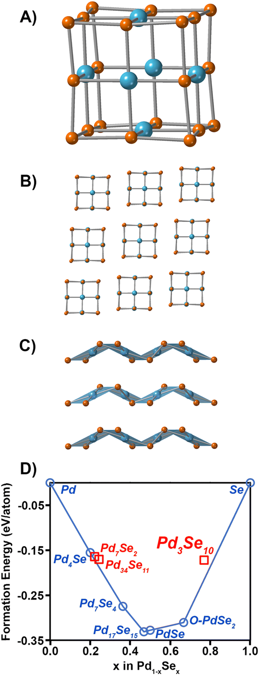 | ||
| Fig. 1 (A) Structure of a Pd6Se20 cluster. Pd atoms are in blue and Se atoms are in orange. (B) Crystal structure of Pd3Se10 looking down the [11] zone axis. (C) Crystal structure of O-PdSe2 looking down the b axis. (D) Pd–Se convex hull phase diagram. Red squares correspond to metastable phases, blue circles correspond to thermodynamically stable phases, and the blue line is the convex hull. | ||
Improving the reliability of the Pd3Se10 synthesis
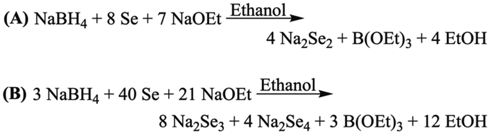
Pd3Se10 was originally synthesized by reacting Na2Se2 and Na2PdCl4 in triethylene glycol.30 Although this method was successful, the synthesis was highly irreproducible, with variable yields ranging from 1% to 65%. We hypothesized that the root of the issue was that the originally proposed reaction is not electrochemically balanced. If we assume Pd3Se10 is comprised of Pd2+ cations, each Se atom should have an overall oxidation state of −0.6 to form a charge balanced phase. Thus, the formation of Pd3Se10 from the reaction between Na2Se2 (which has a Se−1 oxidation state) and Na2PdCl4 would require an additional sacrificial oxidant. Instead, a new chemically and electrochemically balanced equation for the synthesis of Pd3Se10 was proposed (Scheme 1). In this reaction, Na2Se2 was replaced with a mixture of Na2Se3 and Na2Se4 at a 2![[thin space (1/6-em)]](https://www.rsc.org/images/entities/char_2009.gif) :1 molar ratio, in which Se would have an average oxidation state of −0.6. For simplicity, this combination of Na2Se3 and Na2Se4 will be referred to as “Na2Se3.33”, which reflects the atomic ratio of Na to Se in the new precursor, as well as the fact that it is composed of polyselenide dianions.
:1 molar ratio, in which Se would have an average oxidation state of −0.6. For simplicity, this combination of Na2Se3 and Na2Se4 will be referred to as “Na2Se3.33”, which reflects the atomic ratio of Na to Se in the new precursor, as well as the fact that it is composed of polyselenide dianions.
 | ||
| Scheme 1 Solution-phase method for synthesizing Pd3Se10 utilizing Na2Se3 and Na2Se4. | ||
Na2Se2 can be made using a modified version of Klayman's method, in which Se is reduced by NaBH4 in an ethanol solution containing sodium ethoxide (Scheme 2A).45 To synthesize Na2Se3.33, the ratio of NaBH4 to Se was altered so that less Se atoms would be reduced, making the average oxidation state of Se in the polyselenide dianion product less negative (Scheme 2B). The actual product was 63.9(7) mol% Na2Se3 and 36.1(5) mol% Na2Se4, as determined by Rietveld analysis (Fig. S1 and Table S2, ESI†).
 | ||
| Scheme 2 Synthetic scheme for (A) sodium diselenide45 and a (B) 2:1 molar mixture of sodium triselenide and sodium tetraselenide. Et = Ethyl. | ||
In the process of synthesizing this new sodium polyselenide precursor, we also solved the crystal structure of Na2Se3 from the powder X-ray diffraction (PXRD) data of the product containing Na2Se3 and Na2Se4. Although two separate papers have reported synthesizing Na2Se3 in liquid ammonia and also provided supporting UV-visible spectroscopy and 77Se NMR evidence that what they synthesized contained triselenide dianions,46,47 the crystal structure of Na2Se3 has not been reported until now. To solve the crystal structure of Na2Se3, its lattice parameters and possible space groups were first determined using the auto-indexing function in TOPAS for the peaks in the pattern that could not be attributed to Na2Se4. Next, the likely number of formula units per unit cell (Z) for Na2Se3 was inferred from its cell volume (502 Å3) and the assumption that its density would be similar to the two reported sodium polyselenides: Na2Se2 (3.38 g cm−3)48 and Na2Se4 (3.79 g cm−3).49 Assuming a possible density range of 3–4 g cm−3, the only possible integer Z value for Na2Se3 would be 4. With all of this information, a likely crystal structure was found using the Monte Carlo parallel tempering algorithm in FOX.50 Lastly, a Rietveld refinement was performed using GSAS-II to determine the crystal structure of Na2Se3 as well as the weight and mole fractions of Na2Se3 and Na2Se4 in the sodium polyselenide precursor (Fig. S1 and Table S2, ESI†).31
Na2Se3 crystallizes in the monoclinic C2/c space group and, as expected, it consists of sodium cations and triselenide dianions (Fig. S2 and Tables S3, S4, ESI†). It has a reduced crystal symmetry in comparison to the other alkali metal triselenides K2Se3, Rb2Se3, and Cs2Se3, which all share the same orthorhombic K2S3 structure type.51,52 Despite its differences in crystal symmetry, the Se–Se bond length (2.423 Å) and the Se–Se–Se bond angle (102.8°) of the triselenide dianion in Na2Se3 are in close agreement with what is reported for the other three alkali metal triselenides (Table S5, ESI†).
Optimizing the Pd3Se10 synthesis
With the Na2Se3.33 precursor ready for use, we then sought to optimize the solution phase synthesis of Pd3Se10 by tuning three parameters: reaction time, temperature, and Na2PdCl4 injection rate. The PXRD data for the results of the Pd3Se10 syntheses are shown in Fig. 2 and a summary of the different reaction conditions and results is provided in Table S1 (ESI†). For all reactions, a 60 °C solution of Na2PdCl4 was added to a hot solution of Na2Se3.33, which was connected to a Schlenk line to maintain air-free conditions. The Na2PdCl4 precursor was added either all at once (fast addition) or at a target average injection rate.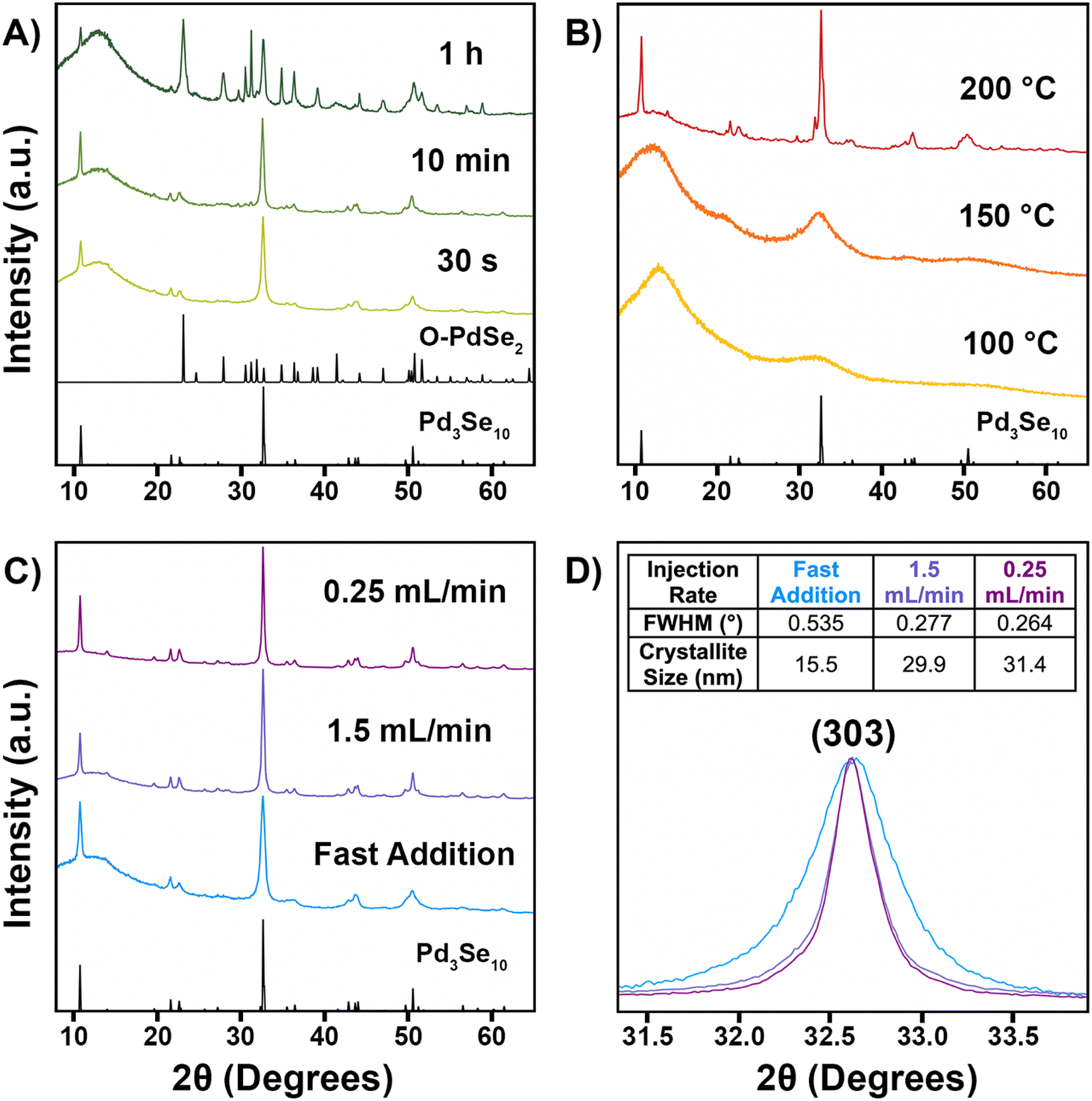 | ||
| Fig. 2 PXRD patterns for various Pd3Se10 synthesis attempts. Pd3Se10 and O-PdSe2 reference patterns are shown in black.30,53 (A) Results for syntheses of different reaction times, but the same temperature (245 °C) and Na2PdCl4 injection rate (fast addition). (B) Results for syntheses at different temperatures, but the same reaction time (1 h) and Na2PdCl4 injection rate (fast addition). (C) Results for syntheses at different Na2PdCl4 injection rates, but the same temperature (200 °C). The fast addition and 1.5 mL min−1 experiments were 10 min long and the 0.25 mL min−1 experiment was 1 h long. (D) Zoomed-in view of the (303) peak for the patterns in (C). The table inset lists the full width at half maximum (FWHM) values for the (303) peaks and the corresponding crystalline domain sizes that were calculated using the Scherrer equation.54 The broad peak around 15° in the PXRD patterns is due to the amorphous plastic sample holder used during data collection. | ||
First, the effect of reaction time was investigated (Fig. 2A) for reactions conducted at the same reaction temperature (245 °C) and injection rate (fast addition). Pd3Se10 crystallizes within 30 s, but O-PdSe2 and Se start to form soon after, with minor peaks corresponding to O-PdSe2 first appearing in the pattern for the 3 min reaction (Fig. S3, ESI†). After 1 h, O-PdSe2 had become a major component in the product, in addition to Pd3Se10. This trend is similar to what was observed for our original reaction using the Na2Se2 precursor, in which longer reactions at 245 °C led to the formation of the thermodynamically stable O-PdSe2 phase and the disappearance of the metastable Pd3Se10 phase.30
Second, the effect of reaction temperature was investigated (Fig. 2B) for 1 h reactions with a fast addition of the Na2PdCl4 precursor. Since lower activation energies are needed to synthesize metastable phases,55 our goal was to find a temperature high enough to form crystalline Pd3Se10, but low enough to avoid the formation of O-PdSe2. Only amorphous products formed for the 100 °C and 150 °C reactions, indicating that these temperatures were too low to provide the necessary energy to form any crystalline palladium selenide phase. However, Pd3Se10 did form for the 200 °C reaction, in addition to selenium and an unknown minor impurity. The impurity peaks are highlighted in Fig. S4 (ESI†). Although the structure of this impurity couldn’t be identified, it is likely a metastable product since it was able to form at 200 °C, but not at 245 °C. Additionally, the lack of peaks in the PXRD pattern corresponding to O-PdSe2 indicate that 200 °C is a low enough temperature to avoid the formation of thermodynamic phases.
For a 10 min reaction at 200 °C, with a fast addition of the Na2PdCl4 solution, Pd3Se10 formed without the presence of any impurities (Fig. 2C). Although this result validated our hypothesis that using a lower temperature would allow for the synthesis of phase pure Pd3Se10, the product formed had broad XRD peaks indicative of small crystalline domain sizes. Since using a slower injection rate typically leads to the synthesis of larger nanoparticles,56–60 we hypothesized that altering this parameter could also be used to create larger crystalline domains of Pd3Se10.
The effect of the Na2PdCl4 injection rate was investigated for syntheses performed at 200 °C, in an effort to improve the crystallinity of the Pd3Se10 product (Fig. 2C). Qualitatively, a slower injection rate produced larger crystalline domain sizes, as evidenced by the sharper peaks present in the PXRD pattern for the 10 min reaction with an average injection rate of 1.5 mL min−1. Slowing the injection rate even further to 0.25 mL min−1 for a 1 h reaction produced slightly sharper PXRD peaks and also prevented the formation of any of the aforementioned impurities that were observed with a fast precursor addition (Fig. 2B and C). To quantify how much the crystallinity of the Pd3Se10 product improved by using slower injection rates, the full width at half maximum (FWHM) values of the (303) peaks were compared (Fig. 2D). Using these values, the crystalline domain sizes of the samples were calculated using the Scherrer equation (Fig. 2D inset).54 The FWHM values for both samples made using the slower injection rates was about twice as small as the value for the sample made with a fast precursor addition. This corresponds to average crystalline domain sizes of approximately 30 nm for both slow injection samples and 15 nm for the fast addition sample.
Electron microscopy was used to further characterize the structure of the Pd3Se10 product, as well as its particle size and morphology (Fig. 3). The atomic resolution HAADF-STEM image of a Pd3Se10 particle was taken to show how the Pd6Se20 clusters pack together and the overlay highlights the match between the atomic number (Z) contrast observed in the image and the expected crystal structure (Fig. 3A). Fig. 3B shows a typical TEM image of an aggregate of Pd3Se10 particles. Pure Pd3Se10 samples had similar particle sizes regardless of their crystalline domain sizes that were calculated using the Scherrer equation. The particles had edge lengths ranging from 10–70 nm, but over 60% of the particles for both samples that were measured had edge lengths in the 20–40 nm range (Fig. S5, ESI†). Fig. 3C shows the corresponding selected area electron diffraction (SAED) ring pattern for the aggregate of Pd3Se10 particles and the indexing is shown in Fig. S6 and Table S6 (ESI†). The measured d-spacings match well with the actual Pd3Se10d-spacings and the most intense ring in the SAED pattern and the most intense peak in the PXRD data correspond to the same (303) reflection. Lastly, energy-dispersive X-ray spectroscopy (EDX) for Pd3Se10 confirmed the expected atomic ratio of Pd to Se (Fig. S7 and Table S7, ESI†).
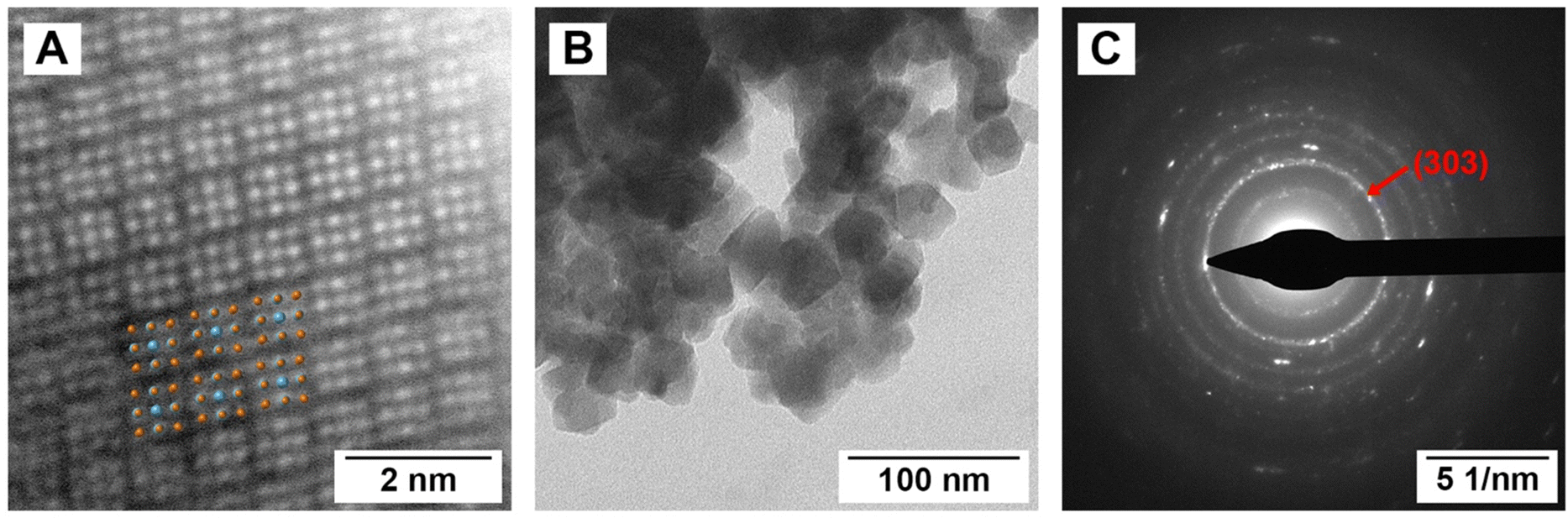 | ||
| Fig. 3 (A) HAADF-STEM image of a Pd3Se10 particle looking down the [11] zone axis, with the crystal structure overlayed on a section of the image. The orange spheres correspond to Se atoms, the blue spheres correspond to Pd atoms. (B) TEM image of an aggregate of Pd3Se10 particles and (C) the corresponding SAED pattern. The most intense ring, corresponding to the (303) reflection, is indicated with the red arrow. | ||
X-ray photoelectron spectroscopy (XPS) data of Pd3Se10 compared to Pd, Se, and O-PdSe2, supports our expectations of the Pd and Se oxidation states in Pd3Se10 (Fig. 4). The Pd 3d5/2 binding energy of Pd3Se10 (336.5 eV) is similar to that of O-PdSe2 (336.7 eV) and 1.2 eV greater than Pd (335.3 eV) (Fig. 4A). The fact that these binding energies are reasonably close in Pd3Se10 and O-PdSe2 supports the assignment of a Pd2+ oxidation state in Pd3Se10. By consequence, the average oxidation state of a Se atom in the material should be −0.6, to maintain charge neutrality. Depending on the nature of charge distribution throughout the Pd6Se20 clusters, this oxidation state could occur with the negative charge delocalized across every Se, or alternatively, with the 12 edge Se atoms having a formal Se−1 charge and the 8 corner atoms being formally Se0. The Se 3d5/2 binding energy of Pd3Se10 (54.6 eV) is closer to that of O-PdSe2 (54.7 eV) than Se (55.2 eV) (Fig. 4B). This indicates that the average Se atom in Pd3Se10 has a negative oxidation state, but it does not allow for a precise oxidation state assignment or provide information on the nature of the delocalization, especially considering the small differences in binding energies between neutral and reduced forms of Se.61–63 Regardless, the combination of the Pd and Se 3d XPS spectra and the square planar geometry of the Pd atoms in the material support this description of the Se oxidation state in Pd3Se10.
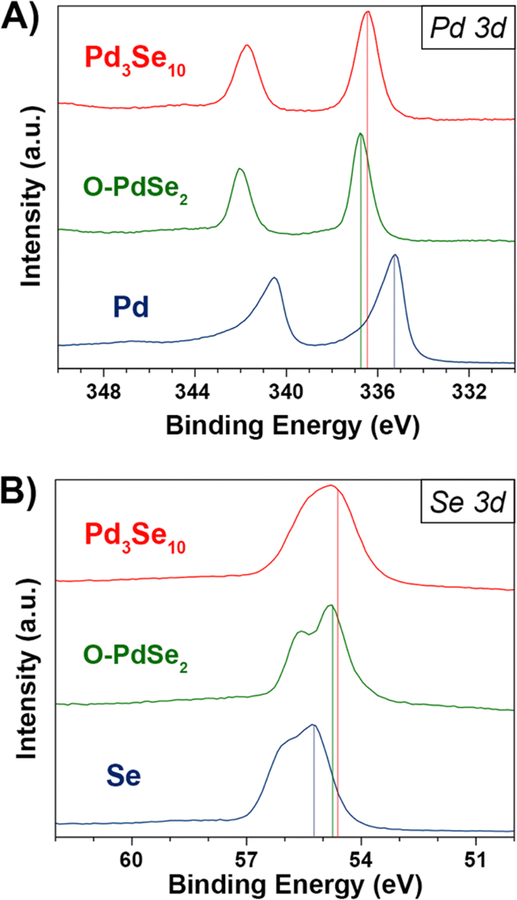 | ||
| Fig. 4 (A) Pd 3d XPS spectra for Pd3Se10, O-PdSe2, and palladium powders. (B) Se 3d XPS spectra for Pd3Se10, O-PdSe2, and selenium powders. | ||
Raman spectroscopy was also used to characterize the Pd3Se10 products to better understand the chemical nature of the amorphous samples grown at 100 °C and 150 °C (Fig. 5). An isolated cluster of Pd6Se20, assuming it has the same molecular symmetry as it has in the crystal structure, would have a D3d point group and 48 vibrational modes (8 A1g, 4 A2g, 12 Eg, 4 A1u, 8 A2u and 12 Eu), of which only the 8 A1g and 12 Eg modes are Raman active. Pd3Se10 crystallizes into the Rm space group with 3 atoms occupying different 18 h Wyckoff sites (x, −x, z), 1 atom occupying the 18g Wyckoff site (x, 0, ½) and 1 atom occupying the 6c site (0, 0, z). Considering only the Raman active modes, each atom on the 18h site would have 2 A1g and 3 Eg modes, each atom on the 18g site would have 1 A1g and 3 Eg modes, and each atom on the 6c site would have 1 A1g and 1 Eg mode. In total, crystalline Pd3Se10 should have 21 Raman active modes (8 A1g and 13 Eg). 20 of these modes correspond to the internal modes of the molecular cluster, whereas the additional Eg mode would correspond to an external mode, or a collective oscillation that involves multiple clusters throughout the crystal. In the crystalline Pd3Se10 spectrum, at least 8 intense Raman modes are observed, which could be either individual modes or combinations of closely spaced Raman modes. Because of the weak van der Waals bonding between Pd6Se20 clusters in the crystal structure, one would expect the frequencies of the internal modes to be only slightly different than an isolated cluster. The Raman spectra of the two amorphous samples (Fig. 5) both had very similar peak positions and relative intensities to the crystalline Pd3Se10 sample. These Raman spectra are clearly distinct from the spectra of selenium, O-PdSe2, and the monoclinic phase of PdSe264 (Fig. S8, ESI†). The fact that the amorphous and crystalline spectra are nearly identical indicate that the amorphous samples are indeed composed of the same Pd6Se20 clusters as crystalline Pd3Se10 but arranged in a disordered manner.
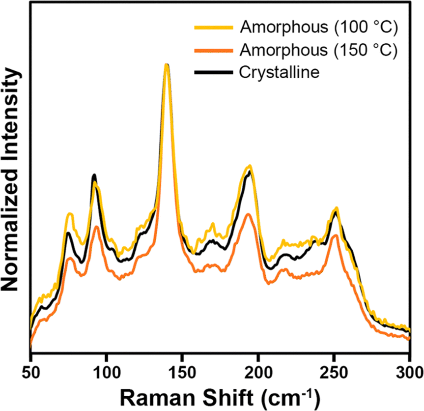 | ||
| Fig. 5 Raman spectra of a crystalline Pd3Se10 sample and the two amorphous Pd3Se10 samples synthesized at 100 °C and 150 °C. | ||
This deeper understanding of the nature of the amorphous Pd3Se10 samples allows us to infer mechanistic information on the formation of crystalline Pd3Se10 in solution. Since an amorphous material composed of Pd6Se20 clusters can form at lower temperatures, this means that the activation energy of forming Pd6Se20 clusters from the Pd and Se precursors is less than the activation energy needed for the clusters to assemble into an ordered extended solid. Consequently, the general mechanism of forming crystalline Pd3Se10 can be thought of as occurring in two steps: an initial faster step to create Pd6Se20 clusters, followed by a slower second step involving the clusters coming together and organizing themselves into a crystalline solid (Fig. S9, ESI†). In actuality, the first step of forming Pd6Se20 clusters must consist of many other elementary steps, such as substitution reactions to replace the chloride ligands in PdCl42− with polyselenide ligands and reactions to allow for Pd atoms to be connected by bridging polyselenide ligands. Obtaining experimental evidence of these elementary steps, however, would require a much more detailed investigation that considers the air-free and high temperature reaction conditions required, as well as the short timescale of cluster formation, and is beyond the scope of this work.
Thermal stability
Since Pd3Se10 is a metastable material, it is critical to know its decomposition temperature, as this sets an upper limit on the possible temperatures it can be synthesized at. To determine the decomposition temperature of Pd3Se10 and gain an understanding of how it decomposes, a simultaneous TGA/DSC experiment was performed for a crystalline Pd3Se10 sample (Fig. 6A). The first significant feature in the DSC curve is an exothermic peak with an onset at 340 °C and a maximum at 350 °C. Although some sample mass loss occurs before 350 °C, the majority happens after the exotherm, as indicated by the large decrease in weight percent in the TGA data. The second feature in the DSC curve is an endotherm that immediately follows the exothermic process. This peak ends at 470 °C, which corresponds to the temperature that the TGA curve begins to flatten out. After the Pd3Se10 sample was heated to 500 °C, a PXRD pattern of the decomposition product was obtained (Fig. 6B). The pattern reveals that O-PdSe2 formed due to the heat treatment and no Pd3Se10 remains.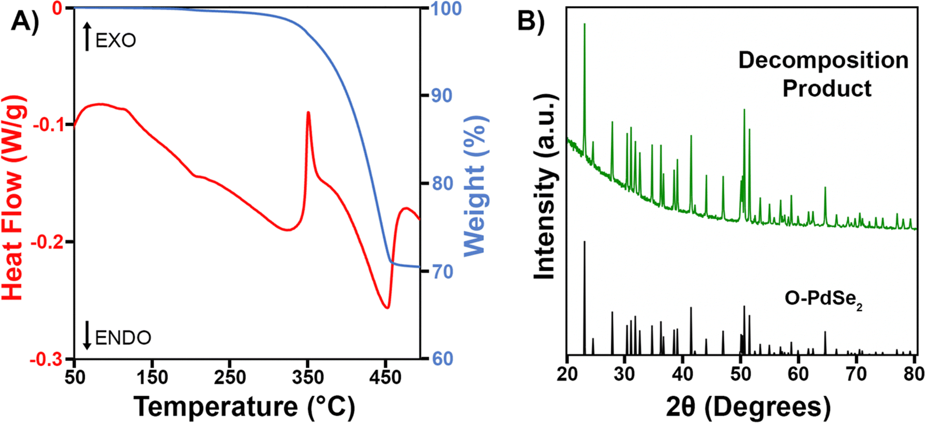 | ||
| Fig. 6 (A) TGA/DSC plot for a crystalline Pd3Se10 sample. (B) PXRD pattern of the decomposition product obtained after heating Pd3Se10 to 500 °C in the TGA instrument. | ||
Taking both the TGA/DSC and PXRD data in Fig. 6 into account, the Pd3Se10 decomposition temperature can be determined and a balanced chemical reaction for the thermal decomposition can be written (Scheme 3). First, we confirmed that the gradual downward slope of the DSC curve before the exotherm does not correspond to a phase transition by acquiring a PXRD pattern of the Pd3Se10 sample after heating it to 300 °C in the TGA instrument (Fig. S10, ESI†). This PXRD pattern shows that heating to 300 °C will not decompose Pd3Se10. However, it does cause a slight decrease in crystalline domain size as indicated by the broadening of the diffraction peaks after heating. Knowing this, the exothermic process at 350 °C can confidently be assigned to the transformation of Pd3Se10 into two more thermodynamically stable phases: O-PdSe2 and selenium. The subsequent endothermic process and sample weight loss can be attributed to the sublimation of selenium, which leaves O-PdSe2 as the only phase remaining after the 500 °C heat treatment. The total weight loss for the TGA experiment is 29.5%, which is very close to the 28.5% weight loss expected for the complete sublimation of the selenium produced by the equation in Scheme 3. The 1% discrepancy in weight percent could be due to the loss of residual solvent from the Pd3Se10 sample.
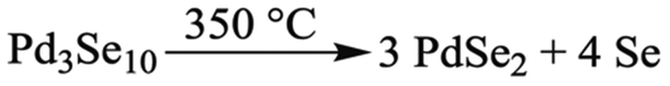 | ||
| Scheme 3 Thermal decomposition reaction of Pd3Se10. | ||
To compare, the thermal stability of an amorphous Pd3Se10 sample was also investigated using TGA/DSC and PXRD (Fig. S11 and S12, ESI†). Amorphous Pd3Se10 undergoes a nearly identical decomposition process as crystalline Pd3Se10. The DSC curve features an exothermic peak with a maximum at 330 °C, immediately followed by an endotherm and an increased rate of weight loss in the TGA plot. The total weight loss for the amorphous sample was 31.0% and the PXRD revealed that the decomposition product was O-PdSe2. The similarity in this decomposition process provides supporting evidence that the amorphous sample is composed of Pd6Se20 clusters.
Optical and electronic properties
Diffuse reflectance spectroscopy (DRS) data of different Pd3Se10 samples was acquired to better understand the material's optical properties (Fig. 7). Fig. 7A shows the Tauc plot of Pd3Se10, assuming an indirect transition, for the sample with a crystalline domain size of 30 nm. This data indicates that Pd3Se10 is an indirect semiconductor with a 1.18 eV band gap. The direct gap occurs at 1.40 eV (Fig. S13, ESI†).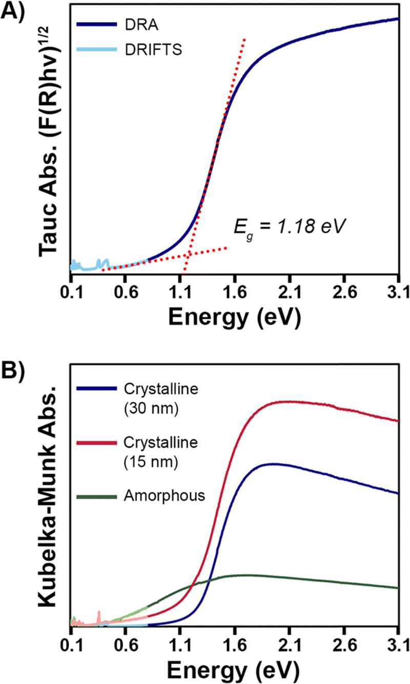 | ||
| Fig. 7 (A) Tauc plot, assuming an indirect transition, for the Pd3Se10 sample with a crystalline domain size of 30 nm, as calculated from the Scherrer equation. (B) Diffuse reflectance spectra, transformed by the Kubelka–Munk function, for amorphous Pd3Se10 and crystalline Pd3Se10 samples with 15 nm and 30 nm domain sizes. The darker-colored (higher energy) part of each spectrum is data collected using diffuse reflectance absorbance (DRA) and the lighter-colored (lower energy) part of each spectrum is data collected using diffuse reflectance infrared Fourier transform spectroscopy (DRIFTS). | ||
Probing deeper, the DRS data for the Pd3Se10 sample with a 30 nm domain size was compared to the sample with a 15 nm domain size and an amorphous sample (Fig. 7B). While the indirect optical gap for the 15 nm sample (1.14 eV) (Fig. S14, ESI†) was very similar to the 30 nm sample's gap, the 15 nm sample's DRS plot featured a broader absorption edge in the Urbach tail region. The Urbach tail is the exponential region of the band edge in between the baseline and linear region in a semiconductor's absorption plot. It is attributed to sub-bandgap absorption caused by a lack of crystallinity, defects, or impurities. The steepness of the Urbach tail can be quantified by the Urbach energy (EU), which helps to assess the relative degree of structural disorder between different samples.35,65–69
The Urbach energies for the 15 and 30 nm Pd3Se10 samples were extracted from the ln(F(R)) vs. energy plots (Fig. S15 and Table S8, ESI†). The EU for the 15 nm sample (0.346 eV) was 1.6 times greater than the EU for the 30 nm sample (0.217 eV). This analysis helps quantitatively show that the 15 nm sample has a larger degree of structural disorder and consequently more sub-bandgap absorption than the 30 nm sample, as would be expected for a material with a smaller crystalline grain size. For the amorphous Pd3Se10 sample, an optical gap was observed at 0.25 eV (Fig. S16, ESI†) and there wasn’t an easily identifiable exponential Urbach tail region in its Kubelka–Munk absorption plot. The greater ensemble of all the various intercluster interactions in this amorphous sample combine to form this significantly reduced optical gap.
The electronic resistivity and photoconductivity measurements on a polycrystalline Pd3Se10 pellet provided further evidence of the material's semiconducting behaviour. Pd3Se10 was pressed into a pellet and sintered at 120 °C to produce a sample with an estimated density of 75%. Electrical contacts on the pellet were made using gold epoxy (Fig. 8a). Two-probe current–voltage measurements at room temperature and in the dark showed ohmic behaviour (Fig. 8b), and based on the pellet dimensions, the material's very high resistivity was estimated to be 3.4 × 10⁷ Ω m. Additionally, when the pellet was illuminated with 532 nm above band gap laser light, the slope of the current–voltage plot increased, indicative of an increase in conductivity (Fig. 8b). Photoexcitation at a power density of 13 mW cm−2 produces a 2% increase in current (Fig. 8c) in less than 1 s. Turning off the illumination leads to a rapid drop in current, followed by a much slower decay back to the initial value. This instantaneous increase in conductivity with above band gap illumination is a common signature of semiconducting behaviour, arising due to the generation of photoexcited electrons and holes. The slow decay kinetics is commonly seen in many semiconducting materials as well, and is indicative of the photoexcited carriers populating long-lived trap states, which is known as persistent photoconductivity.70–72
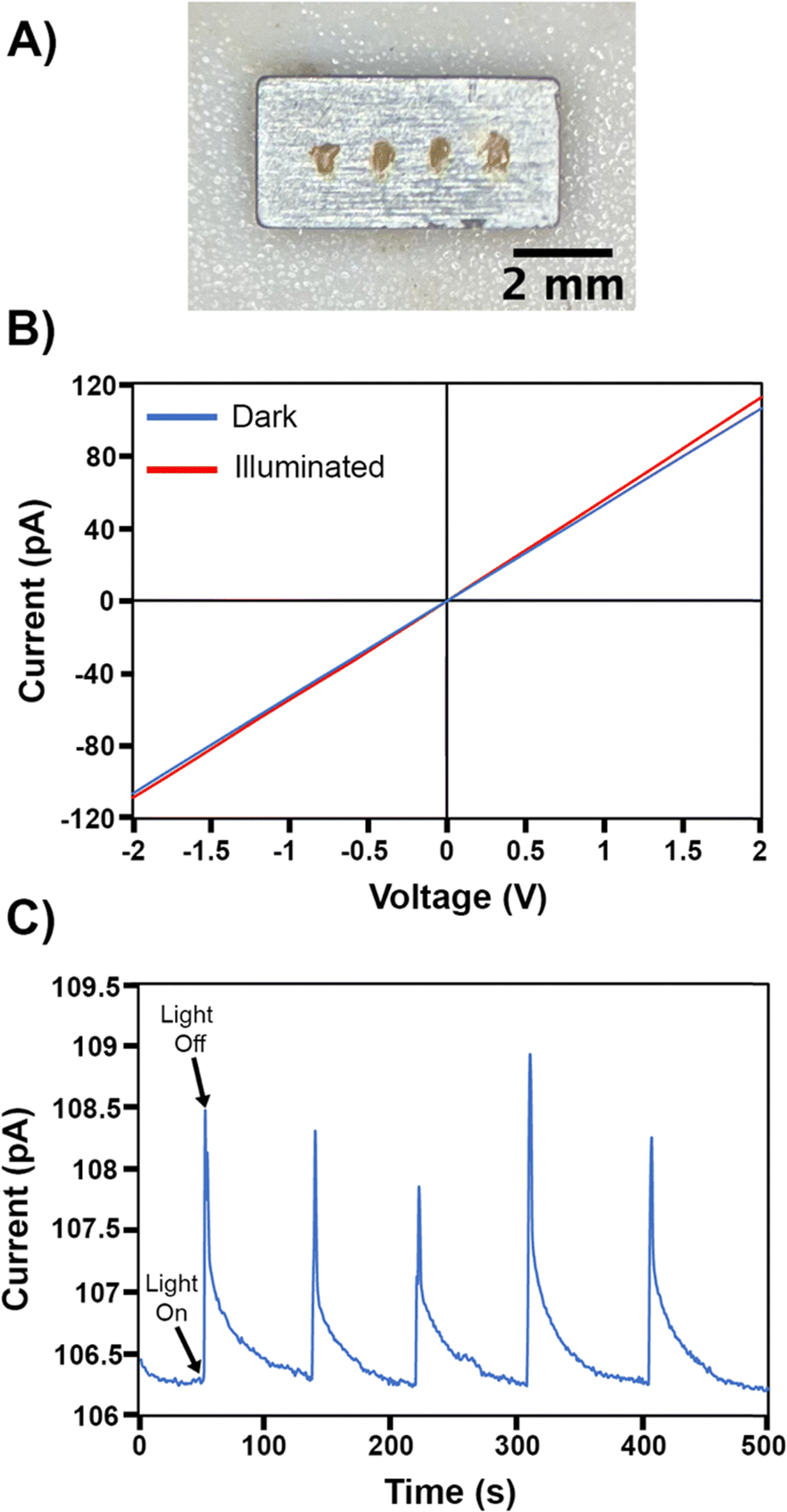 | ||
| Fig. 8 (A) Image of the Pd3Se10 pellet with gold epoxy contacts. (B) Current versus voltage plot for the Pd3Se10 pellet measured in the dark (blue line) and while illuminated with a 532 nm laser (red line). (C) Current versus time plot for the Pd3Se10 pellet showing five light on–off cycles. | ||
Conclusions
Pd3Se10 is a new Pd6Se20 cluster-based semiconducting material that shows intriguing optoelectronic properties. To overcome reproducibility issues that plagued its initial synthetic method, we developed a solution-phase electrochemically balanced reaction utilizing Na2PdCl4 and a 2:1 molar mixture of Na2Se3 and Na2Se4. Under optimized conditions, this reaction allowed for the reliable and high-yield production of crystalline Pd3Se10. The reason that Pd3Se10 can form in solution was also a point of interest, considering that convex hull calculations predict it to be a metastable phase. This prediction was supported experimentally by TGA/DSC and PXRD data which show that it decomposes at 350 °C into the more thermodynamically stable phases O-PdSe2 and Se. Further calculations suggest that the ability of Pd3Se10 to form in solution is likely due to its lower surface energies relative to O-PdSe2. Raman spectroscopy showed that Pd6Se20 clusters were present in both the crystalline sample and the amorphous samples which formed below the optimal synthesis temperature. From this, it was inferred that Pd6Se20 clusters form in solution first before assembling into a crystalline lattice. Lastly, DRS, electrical resistivity, and photoconductivity measurements show that Pd3Se10 is semiconducting, with an indirect band gap of 1.18 eV. Overall, Pd6Se20 is an exciting new entry into the library of superatomic clusters and materials.
Author contributions
C. T. I. and J. E. G. designed and organized the project. C. T. I. and C. W. conducted the synthesis and most characterization of the materials. A. R. and D. W. M. conducted and analysed the HAADF-STEM. Y. K. assisted with the collection and analysis of XPS data. B. Y. and W. W. performed and analysed theoretical computations. T. S. conducted and helped analyse the resistivity and photoconductivity measurements. C. T. I. and J. E. G. wrote the manuscript with contributions from all authors.Data availability
The data supporting this article have been included as part of the ESI.†Conflicts of interest
There are no conflicts to declare.Acknowledgements
J. E. G., C. T. I., B. Y. and W. W. acknowledge the Air Force Office of Scientific Research for primary funding from grant number FA9550-21-1-02684. A. R. and D. W. M. acknowledge the Center for Emergent Materials, an NSF MRSEC, under award number DMR-2011876 for partial support. Electron microscopy was performed at the Center for Electron Microscopy and Analysis (CEMAS) at The Ohio State University. We also thank R. A. Nelson and N. R. Jones for a PdSe2 single crystal for XPS characterization.References
- A. Pinkard, A. M. Champsaur and X. Roy, Acc. Chem. Res., 2018, 51, 919–929 CrossRef CAS PubMed.
- E. A. Doud, A. Voevodin, T. J. Hochuli, A. M. Champsaur, C. Nuckolls and X. Roy, Nat. Rev. Mater., 2020, 5, 371–387 CrossRef.
- S. A. Claridge, A. W. Castleman, Jr., S. N. Khanna, C. B. Murray, A. Sen and P. S. Weiss, ACS Nano, 2009, 3, 244–255 CrossRef CAS PubMed.
- P. Jena and Q. Sun, Chem. Rev., 2018, 118, 5755–5870 CrossRef CAS PubMed.
- O. Peña, Phys. C, 2015, 514, 95–112 CrossRef.
- W. Zhang, W. Zhang, J. Tan, Y. Tang and Q. Gao, Mater. Chem. Front., 2023, 7, 5500–5518 RSC.
- T. Yildirim, O. Zhou and J. E. Fischer, in The Physics of Fullerene-Based and Fullerene-Related Materials, ed. W. Andreoni, Springer Netherlands, Dordrecht, 2000, pp. 67–133 Search PubMed.
- J. E. Fischer, P. A. Heiney and A. B. Smith, III, Acc. Chem. Res., 1992, 25, 112–118 CrossRef CAS.
- S. Scharfe, F. Kraus, S. Stegmaier, A. Schier and T. F. Fässler, Angew. Chem., Int. Ed., 2011, 50, 3630–3670 CrossRef CAS PubMed.
- R. J. Wilson, B. Weinert and S. Dehnen, Dalton Trans., 2018, 47, 14861–14869 RSC.
- P. Jena, J. Phys. Chem. Lett., 2013, 4, 1432–1442 CrossRef CAS PubMed.
- A. W. Castleman, Jr. and S. N. Khanna, J. Phys. Chem. C, 2009, 113, 2664–2675 CrossRef.
- I. Chakraborty and T. Pradeep, Chem. Rev., 2017, 117, 8208–8271 CrossRef CAS PubMed.
- M. Hidai, S. Kuwata and Y. Mizobe, Acc. Chem. Res., 2000, 33, 46–52 CrossRef CAS PubMed.
- M. N. Sokolov and P. A. Abramov, Coord. Chem. Rev., 2012, 256, 1972–1991 CrossRef CAS.
- X. Roy, C.-H. Lee, A. C. Crowther, C. L. Schenck, T. Besara, R. A. Lalancette, T. Siegrist, P. W. Stephens, L. E. Brus, P. Kim, M. L. Steigerwald and C. Nuckolls, Science, 2013, 341, 157–160 CrossRef CAS PubMed.
- Q. Li, J. C. Russell, T.-Y. Luo, X. Roy, N. L. Rosi, Y. Zhu and R. Jin, Nat. Commun., 2018, 9, 3871 CrossRef PubMed.
- J. A. Tulyagankhodjaev, P. Shih, J. Yu, J. C. Russell, D. G. Chica, M. E. Reynoso, H. Su, A. C. Stenor, X. Roy, T. C. Berkelbach and M. Delor, Science, 2023, 382, 438–442 CrossRef CAS PubMed.
- C.-H. Lee, L. Liu, C. Bejger, A. Turkiewicz, T. Goko, C. J. Arguello, B. A. Frandsen, S. C. Cheung, T. Medina, T. J. S. Munsie, R. D’Ortenzio, G. M. Luke, T. Besara, R. A. Lalancette, T. Siegrist, P. W. Stephens, A. C. Crowther, L. E. Brus, Y. Matsuo, E. Nakamura, Y. J. Uemura, P. Kim, C. Nuckolls, M. L. Steigerwald and X. Roy, J. Am. Chem. Soc., 2014, 136, 16926–16931 CrossRef CAS PubMed.
- W.-L. Ong, E. S. O’Brien, P. S. M. Dougherty, D. W. Paley, C. Fred Higgs III, A. J. H. McGaughey, J. A. Malen and X. Roy, Nat. Mater., 2017, 16, 83–88 CrossRef CAS PubMed.
- S. Mandal, A. C. Reber, M. Qian, P. S. Weiss, S. N. Khanna and A. Sen, Acc. Chem. Res., 2013, 46, 2385–2395 CrossRef CAS PubMed.
- K. Liu, L. Liu and T. Zhai, J. Phys. Chem. Lett., 2022, 13, 2173–2179 CrossRef CAS PubMed.
- M. M. Olmstead, A. S. Ginwalla, B. C. Noll, D. S. Tinti and A. L. Balch, J. Am. Chem. Soc., 1996, 118, 7737–7745 CrossRef CAS.
- W. Han, P. Huang, L. Li, F. Wang, P. Luo, K. Liu, X. Zhou, H. Li, X. Zhang, Y. Cui and T. Zhai, Nat. Commun., 2019, 10, 4728 CrossRef CAS PubMed.
- P. Ballirano and A. Maras, Z. Kristallogr. NCS, 2002, 217, 177–178 CAS.
- X. Chen, G. Fei, Y. Song, T. Ying, D. Huang, B. Pan, D. Yang, X. Yang, K. Chen and X. Zhan, J. Am. Chem. Soc., 2022, 144, 20915–20922 CrossRef CAS PubMed.
- X. Feng, X. Peng, B. Peng, Z. Li, W. Huang, S. Yang, K. Pei, Z. Sun, F. Huang, H. Li, Z. Shuai and T. Zhai, J. Am. Chem. Soc., 2021, 143, 20192–20201 CrossRef CAS PubMed.
- G. S. Pawley and R. P. Rinaldi, Acta Crystallogr., Sect. B, 1972, 28, 3605–3609 CrossRef CAS.
- X. Feng, Z. Sun, K. Pei, W. Han, F. Wang, P. Luo, J. Su, N. Zuo, G. Liu, H. Li and T. Zhai, Adv. Mater., 2020, 32, 2003146 CrossRef CAS PubMed.
- C. T. Irvine, N. Hoefer, M. J. Moser, R. A. Nelson, D. W. McComb and J. E. Goldberger, Chem. Mater., 2023, 35, 4404–4411 CrossRef CAS.
- B. H. Toby and R. B. Von Dreele, J. Appl. Crystallogr., 2013, 46, 544–549 CrossRef CAS.
- F. A. Stevie and C. L. Donley, J. Vac. Sci. Technol., A, 2020, 38, 063204 CrossRef CAS.
- J. F. Moulder, W. F. Stickle, P. E. Sobol and K. D. Bomben, Handbook of X-ray Photoelectron Spectroscopy, Perkin-Elmer Corporation, Eden Prarie, MN, 1992 Search PubMed.
- R. A. Nelson, Z. Deng, A. M. Ochs, K. G. Koster, C. T. Irvine, J. P. Heremans, W. Windl and J. E. Goldberger, Mater. Horiz., 2023, 10, 3740–3748 RSC.
- P. Makuła, M. Pacia and W. Macyk, J. Phys. Chem. Lett., 2018, 9, 6814–6817 CrossRef PubMed.
- G. Kresse and J. Furthmüller, Phys. Rev. B: Condens. Matter Mater. Phys., 1996, 54, 11169–11186 CrossRef CAS PubMed.
- K. Lejaeghere, V. Van Speybroeck, G. Van Oost and S. Cottenier, Crit. Rev. Solid State Mater. Sci., 2014, 39, 1–24 CrossRef CAS.
- P. E. Blöchl, Phys. Rev. B: Condens. Matter Mater. Phys., 1994, 50, 17953–17979 CrossRef PubMed.
- I. Hamada, Phys. Rev. B: Condens. Matter Mater. Phys., 2014, 89, 121103 CrossRef.
- S. Grimme, S. Ehrlich and L. Goerigk, J. Comput. Chem., 2011, 32, 1456–1465 CrossRef CAS PubMed.
- A. Navrotsky, Geochem. Trans., 2003, 4, 34 CrossRef PubMed.
- Y. Zeng, N. J. Szymanski, T. He, K. Jun, L. C. Gallington, H. Huo, C. J. Bartel, B. Ouyang and G. Ceder, Sci. Adv., 2024, 10, eadj5431 CrossRef CAS PubMed.
- J. M. McHale, A. Auroux, A. J. Perrotta and A. Navrotsky, Science, 1997, 277, 788–791 CrossRef CAS.
- H. Zhang and J. F. Banfield, J. Mater. Chem., 1998, 8, 2073–2076 RSC.
- X. Yang, Q. Wang, Y. Tao and H. Xu, J. Chem. Res., 2002, 2002, 160–161 CrossRef.
- J. Cusick and I. Dance, Polyhedron, 1991, 10, 2629–2640 CrossRef CAS.
- K. W. Sharp and W. H. Koehler, Inorg. Chem., 1977, 16, 2258–2265 CrossRef CAS.
- H. Föppl, E. Busmann and F.-K. Frorath, Z. Anorg. Allg. Chem., 1962, 314, 12–20 CrossRef.
- J. Getzschmann, E. Rönsch and P. Böttcher, Z. Kristallogr. - New Cryst. Struct., 1997, 212, 87 CAS.
- V. Favre-Nicolin and R. Cerny, J. Appl. Crystallogr., 2002, 35, 734–743 CrossRef CAS.
- V. P. Böttcher, Z. Anorg. Allg. Chem., 1977, 432, 167–172 CrossRef.
- V. P. Böttcher, Z. Anorg. Allg. Chem., 1980, 461, 13–21 CrossRef.
- C. Soulard, X. Rocquefelte, P.-E. Petit, M. Evain, S. Jobic, J.-P. Itié, P. Munsch, H.-J. Koo and M.-H. Whangbo, Inorg. Chem., 2004, 43, 1943–1949 CrossRef CAS PubMed.
- C. F. Holder and R. E. Schaak, ACS Nano, 2019, 13, 7359–7365 CrossRef CAS PubMed.
- G. Bhaskar, V. Gvozdetskyi, S. L. Carnahan, R. Wang, A. Mantravadi, X. Wu, R. A. Ribeiro, W. Huang, A. J. Rossini, K.-M. Ho, P. C. Canfield, O. I. Lebedev and J. V. Zaikina, ACS Mater. Au, 2022, 2, 614–625 CrossRef CAS PubMed.
- B. K. Park, S. Jeong, D. Kim, J. Moon, S. Lim and J. S. Kim, J. Colloid Interface Sci., 2007, 311, 417–424 CrossRef CAS PubMed.
- O. B. Achorn, D. Franke and M. G. Bawendi, Chem. Mater., 2020, 32, 6532–6539 CrossRef CAS.
- J. Park, B. Koo, Y. Hwang, C. Bae, K. An, J.-G. Park, H. M. Park and T. Hyeon, Angew. Chem., Int. Ed., 2004, 43, 2282–2285 CrossRef CAS PubMed.
- B. Koo, J. Park, Y. Kim, S.-H. Choi, Y.-E. Sung and T. Hyeon, J. Phys. Chem. B, 2006, 110, 24318–24323 CrossRef CAS PubMed.
- D. Kim, S. Jeong and J. Moon, Nanotechnology, 2006, 17, 4019 CrossRef CAS PubMed.
- M. Shenasa, S. Sainkar and D. Lichtman, J. Electron Spectrosc. Relat. Phenom., 1986, 40, 329–337 CrossRef CAS.
- J. Wu, H. Ma, C. Zhong, M. Wei, C. Sun, Y. Ye, Y. Xu, B. Tang, Y. Luo, B. Sun, J. Jian, H. Dai, H. Lin and L. Li, Nano Lett., 2022, 22, 6816–6824 CrossRef CAS PubMed.
- J. Fan, X. Hu, W. Qin, M. Zhou, Z.-Y. Liu, S.-J. Gao, L.-P. Tan, L.-B. Luo and W. Zhang, ACS Appl. Nano Mater., 2023, 6, 2672–2681 CrossRef CAS.
- E. Selb, M. Tribus and G. Heymann, Inorg. Chem., 2017, 56, 5885–5891 CrossRef CAS PubMed.
- E. Ugur, M. Ledinský, T. G. Allen, J. Holovský, A. Vlk and S. De Wolf, J. Phys. Chem. Lett., 2022, 13, 7702–7711 CrossRef CAS PubMed.
- J. Klein, L. Kampermann, B. Mockenhaupt, M. Behrens, J. Strunk and G. Bacher, Adv. Funct. Mater., 2023, 33, 2304523 CrossRef CAS.
- M. Li, P. Huang and H. Zhong, J. Phys. Chem. Lett., 2023, 14, 1592–1603 CrossRef CAS PubMed.
- C. Witt, K. Schötz, A. Köhler and F. Panzer, J. Phys. Chem. C, 2024, 128, 6336–6345 CrossRef CAS.
- K. Kumar, O. V. Rambadey and P. R. Sagdeo, J. Phys. Chem. C, 2023, 127, 22164–22176 CrossRef CAS.
- R. J. Freitas and K. Shimakawa, Photoconductivity and Photoconductive Materials, 2022, pp. 549–576 Search PubMed.
- S.-L. Gao, L.-P. Qiu, J. Zhang, W.-P. Han, S. Ramakrishna and Y.-Z. Long, ACS Appl. Electron. Mater., 2024, 6, 1542–1561 CrossRef CAS.
- M. Sofos, J. Goldberger, D. A. Stone, J. E. Allen, Q. Ma, D. J. Herman, W.-W. Tsai, L. J. Lauhon and S. I. Stupp, Nat. Mater., 2009, 8, 68–75 CrossRef CAS PubMed.
Footnote |
| † Electronic supplementary information (ESI) available. See DOI: https://doi.org/10.1039/d4tc03743j |
| This journal is © The Royal Society of Chemistry 2025 |