
Enhanced electrical properties of lead-free sodium potassium niobate piezoelectric ceramics prepared via cold sintering assisted sintering†
Yao
Huang
a,
Xinyue
Song
a,
Renbing
Sun
b,
Hai
Jiang
a,
Peng
Du
 a and
Laihui
Luo
*a
a and
Laihui
Luo
*a
aDepartment of Microelectronics Science and Engineering, School of Physical Science and Technology, Ningbo University, Ningbo, 315211, China. E-mail: luolaihui@nbu.edu.cn
bCollege of Materials Science and Engineering, Ningbo University of Technology, Ningbo 315016, China
First published on 7th November 2024
Abstract
It is a great challenge to prepare dense (K,Na)NbO3 (KNN)-based ceramics with low volatilization of K+/Na+ ions utilizing a conventional solid state reaction method. Herein, ternary KNNS–BNZS–BZ ceramics were prepared utilizing the conventional solid state reaction sintering (CS) method and the cold sintering-assisted sintering (CSAS) process. The CSAS process was used to prepare discs using KMnO4 solution as a transient melt and held at 225 °C under a uniaxial pressure of 380 MPa for 30 min. The microstructures and piezoelectric properties of the prepared ceramics were investigated. The density and piezoelectric performances of the ceramics prepared via CSAS are much superior to those of the counterparts by the conventional solid-state reaction. The piezoelectric constant d33 of the CSAS ceramic with strong ferroelectric properties reaches a high value of ∼470 pC N−1. The XRD Rietveld refinement, dielectric–temperature curves and TEM show that the prepared KNNS–BNZS–BZ ceramics have a state of three-phase rhombohedral–orthorhombic–tetragonal (R–O–T) coexistence at room temperature. The enhanced piezoelectric properties of the CSAS ceramics are ascribed to the improved densification and reduced volatilization of K+/Na+ ions by the strategy of CSAS. The present investigation shows that the CSAS method is a potential route for the preparation of KNN-based ceramics.
1. Introduction
The discovery of Pb(Ti,Zr)O3 (PZT) ceramics with excellent piezoelectric performances is a milestone in the history of piezoelectric ceramics, and they are occupying the major markets of piezoelectric materials.1–5 However, the production, application and recycling of lead oxide cause serious harm to human health and the natural environment.4–7 Hence, the development of high-performance lead-free substitutes has become particularly urgent. (K,Na)NbO3 (KNN)-based lead-free piezoelectric ceramics have the potential to replace lead-based ceramics due to their advantages such as high Curie temperature and high piezoelectric properties.1,8,9 In 2004, Saito10et al. prepared KNN-based lead-free piezoelectric ceramics with a high piezoelectric coefficient d33 of 416 pC N−1via texture technology and phase boundary design, which makes the KNN-based ceramics attract much attention. It is a feasible method to construct rhombohedral–orthorhombic (R–O) phase, orthorhombic–tetragonal (O–T) phase or rhombohedral–tetragonal (R–T) phase boundaries in KNN-based ceramics for obtaining excellent piezoelectric performances.1,4,11–13It has been reported that alternative B-site Nb is usually used to construct multiphase boundaries to improve the piezoelectricity of KNN-based ceramics, in which the Sb element has been shown to move both R–O and O–T phase boundaries to near room temperature.1,14,15 Bi0.5M0.5NO3 (M = K, Na, Li, Ag; N = Ti, Zr, Sn, Hf) has a similar effect to that of the Sb element and also can also move the R–O and O–T phase boundaries to near room temperature.14,16 On the other side, BaZrO3 (BZ) is added to KNN-based ceramics to significantly move their R–O phase boundaries towards room temperature, thus increasing the piezoelectric properties of KNN-based ceramics.14,17 Zhou18et al. designed a composition of 0.96(K0.48Na0.52)(Nb0.96Sb0.04)O3–0.03BaZrO3–0.01(Bi0.5Na0.5)ZrO3, which shows a high piezoelectric coefficient d33 of ∼ 300 pC N−1 and a large electromechanical coupling factor kp of ∼ 0.56. Ma19et al. designed a composition of (0.99 − x)K0.5Na0.5Nb0.96Sb0.04O3–0.01BaZrO3–xBi0.5Na0.5ZrO3, and the ceramics showed good electrical properties (d33 ∼ 450 pC N−1 and TC ∼ 252 °C). Shi20et al., designed a composition of (0.98−x)K0.525Na0.475Nb0.965Sb0.035O3–0.02BaZr0.5Hf0.5O3–x(Bi0.5Na0.5)ZrO3 with good comprehensive properties (d33 ∼ 410 pC N−1, TC ∼ 255 °C, Suni ∼ 0.132%, and  ). Zhang21et al. designed a composition of (0.97−x)K0.5Na0.5Nb0.965Sb0.035O3–0.03Bi0.5Na0.5Zr0.8Sn0.2O3–xBaZrO3 (KNNS–BNZS–xBZ), and the phase structure of the ceramics was adjusted via BaZrO3; the obtained ceramics showed a high piezoelectric constant d33 of 454 pC N−1 and a Curie temperature TC of 241 °C.
In addition, it is difficult to fabricate KNN-based ceramics with high densities by conventional solid-state reaction sintering (CS) due to the volatilization of K2O and Na2O at high temperature, and the electrical properties of the ceramics are unsatisfactory due to the deviation from a stoichiometric ratio.22 Recently, a new sintering technique known as the cold sintering process (CSP) can achieve 80–99% of the theoretical density, which allows the ceramics to obtain densification at a low temperature by introducing a transient solvent that dissolves the particle edges with the aid of pressure and temperature while facilitating the particle rearrangement.23–26 Densified ceramics, such as KH2PO4, NaNO2,1 BaTiO3,23,27 and Na0.5Bi0.5TiO3,28 were successfully prepared using the CSP. The CSP has been shown to be a feasible method for the preparation of dense ceramics at low temperatures due to the advantages of simple equipment, the ease of operation, and low sintering temperatures compared to other sintering techniques. For some specific compositions, although they could not be densified directly by the CSP, the samples treated by the CSP method maintain the potassium-rich phase, and the prepared green density is enhanced and the volatilization of alkali ions is minimized. For example, Ma24et al. increased the green density of KNN from 53% to over 65% via the CSP and successfully reduced the sintering temperature of KNN ceramics from 1200 to 1055 °C in the following conventional high temperature sintering process. This method is derived from the CSP and then followed by conventional sintering or heat treatment and can be called cold sintering assisted sintering (CSAS). It has been demonstrated that the CSAS method can play a positive role in increasing the green density of ceramics and lowering the sintering temperatures. Therefore, the present work intends to introduce KMnO4 solution as a transient solvent to investigate the effect of the CSP on the electrical properties of 0.955K0.5Na0.5Nb0.965Sb0.035O3–0.03Bi0.5Na0.5Zr0.8Sn0.2O3–0.015BaZrO3 (KNNS–BNZS–BZ) ceramics.
2. Experimental section
2.1 Preparation process
Lead free KNNS–BNZS–BZ ceramic powders were prepared by a solid-state reaction method. The raw materials, Na2CO3 (99.8%), Nb2O5 (99.9%), K2CO3 (99.5%), Sb2O3 (99.9%), ZrO2 (99%), Bi2O3 (99.9%), SnO2 (99.5%) (Shanghai Aladdin Bio-Chem Technology Co., Ltd) and BaCO3 (99%) (Sinopharm Chemical Reagent Co., Ltd), were weighed based on the stoichiometric ratio after drying at 80 °C for 8 h to remove the absorbed water. Carbonates and oxides were mixed by ball milling at 380 rpm for 12 h in a planetary ball-mill using ethanol solution as the milling medium and agate as milling balls. The slurry was dried and calcined at 850 °C for 6 h to obtain the powders. 0.35 g of powders was taken and pressed to form a disc with a diameter of 10 mm and a thickness of ∼1.5 mm (named the CS sample). For comparison, the same powders were mixed with 0.2 ml, 0.34 mol% KMnO4 solution, and hand-milled for 5 min. The obtained mixtures were loaded into a steel die with 10 mm in diameter and uniaxially pressed into pellets under 380 MPa. Both a heater jacket and a pressure equipped with two hot plates were applied to increase the temperature to 225 °C, and the uniaxial pressure of 380 MPa was applied for 30 minutes, resulting in a disc with a diameter of 10 mm and a thickness of about 1.5 mm (named the CSAS sample). Subsequently, both CSAS and CS discs were sintered in the same batch at 1090–1120 °C for 3 h. Accordingly, the obtained samples are named CSAS-1090, CSAS-1100, CSAS-1110, CSAS-1120 and CS-1090, CS-1100, CS-1110, and CS-1120.The sintered disc ceramics were ground to 1 mm in thickness and polished with a diamond paste. For the characterization of electrical properties and electrical poling, silver electrodes were coated onto both sides of the samples and sintered at 600 °C for 30 min. The samples were pooled in silicone oil at 120 °C under an electric field of 4 kV mm−1 for 30 min.
2.2 Material characterization
The Archimedes method was used to test the densities of the sintered specimens. The phase structure of the ceramic was analyzed using a powder X-ray diffraction (XRD) analyzer with Cu-Kα radiation (D8 Advance, Bruker, Germany). The surface microstructure of the ceramics was obtained using a scanning electron microscope (SEM, Hitachi SUS-700). The piezoelectric constant of the ceramics was tested with a Belin-court meter (ZJ-3A, Institute of Acoustic, Chinese Academy of Sciences, China). The current–electric field (I–E) and polarization–electric field (P–E) hysteresis loops were recorded using an ferroelectric analyzer (Premier II, Radiant Technologies, United States). A DMS-1000 dielectric temperature spectrum measuring system (Partulab, Wuhan, China) combined with an Agilent 4294A impedance analyzer was employed to obtain the variation of dielectric performances from 30 to 300 °C at different frequencies. A TZDM-200-300 low temperature dielectric measuring system was employed to obtain the variation of dielectric performances from −150 to 150 °C at different frequencies. The mechanical quality factor Qm and the electromechanical coupling coefficient kp were measured at room temperature using an Agilent 4294A impedance analyzer. The electric field induced strain S was measured using an ferroelectric measurement system TF Analyzer 2000E (aixACCT Systems GmbH, Aachen, Germany). The XPS spectra were obtained using an Omicron Sphera II hemispherical electron energy analyzer. A commercial atomic force microscope (AFM) (Asylum Research Cypher-HV) with a mode of piezoelectric force microscopy (PFM) was used to observe ferroelectric domains of the ceramics. Atomic-resolution high-angle annular dark field (HAADF) and annular bright field (ABF) images were acquired using an atomic-resolution STEM (an aberration–corrected Titan Themis G2 microscope) and the accurate polarization vectors in the STEM images were clarified via 2D Gaussian peak fitting.3. Results and discussion
Fig. 1(a) shows the XRD patterns of CS-1110 and CSAS ceramics. No impurity phase is observed under the detection resolution of the XRD instrument, indicating that the prepared ceramics have a pure perovskite phase at room temperature. The enlarged XRD patterns in the range of 2θ from 45° to 47° are shown in Fig. 1(b). As the sintering temperature increases to 1120 °C, the XRD peaks of CSAS ceramics seem to shift towards the larger angle, which may be due to the enhanced volatilization of the A-site elements K+ and Na+ at higher temperature, which creates numerous oxygen vacancies.24 As a result, the crystal lattice decreases. The pioneer work has demonstrated that the phase structure greatly determines the piezoelectric performances of KNN-based ceramics.29,30 For KNN-based piezoelectric ceramics, the phase structure can be roughly quantified according to the relative intensities of (002) and (200) peaks (I002/I200). For orthorhombic ceramics with a random orientation, the I002/I200 ratio is equal to 2![[thin space (1/6-em)]](https://www.rsc.org/images/entities/char_2009.gif) :1, while for tetragonal ceramics, this ratio becomes 1:2.2,31,32 Observing the diffraction peak characteristics and peak intensities near 2θ = 45°, it can be preliminarily concluded that all the prepared ceramics are mixed-phase structures.
:1, while for tetragonal ceramics, this ratio becomes 1:2.2,31,32 Observing the diffraction peak characteristics and peak intensities near 2θ = 45°, it can be preliminarily concluded that all the prepared ceramics are mixed-phase structures.
 | ||
| Fig. 1 (a) XRD patterns of CS-1110 and CSAS ceramics. (b) Zoom-in XRD patterns in the 2θ range from 44° to 47°. | ||
The SEM micrographs of representative CS-1110 and CSAS ceramics are shown in Fig. 2. Before measuring, all ceramics were polished and thermally etched at 900 °C for 2 hours. The ceramics prepared by the CSAS method are significantly denser and have larger grain sizes than that prepared by the traditional solid-reaction method. This phenomenon is attributed to the formation of a liquid phase of MnO2 produced by the decomposition of KMnO4 during the sintering process, which promotes mass transport,33,34 and the presence of an amorphous potassium-rich phase on the surface of the KNN particles increases the interfacial energy of the particles, which facilitates the growth of the grains. By comparing the CSAS ceramics sintered at different temperatures, the proportion occupied by small grains in the ceramics increases with the increase of the sintering temperature, which fills up the voids between the large grains. The morphology shows a bimodal grain distribution, which is very favorable for the dense microstructure.2 Higher densities and larger grains are obtained for CSAS ceramics, which is favorable for obtaining high piezoelectric properties.
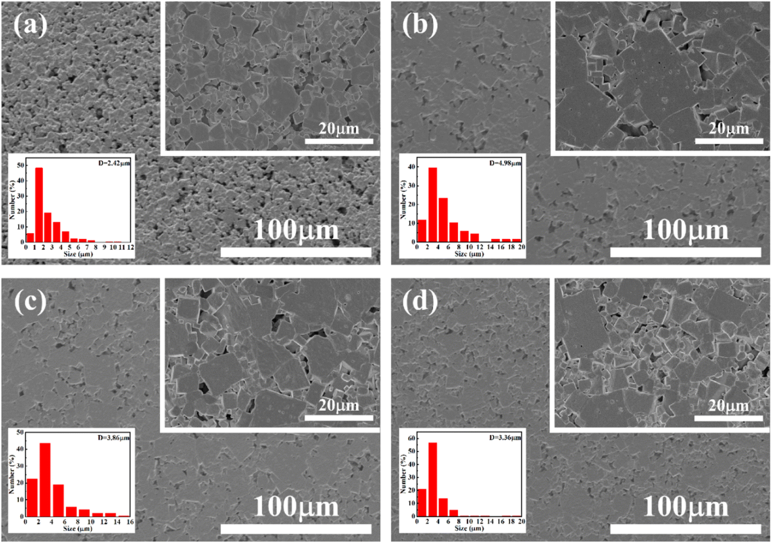 | ||
| Fig. 2 SEM images of (a) CS-1110, (b) CSAS-1090, (c) CSAS-1110, and (d) CSAS-1120 ceramics. The inset is the zoom-in SEM images and grain size distributions. | ||
Fig. 3(a) shows the d33 values of the CS and CSAS ceramics. The d33 values of ceramics prepared by the two methods have a similar trend with the sintering temperature, both an increase and then a decrease with the temperature. The highest piezoelectric coefficients are obtained at 1110 °C. The d33 value of the CSAS samples is higher than that of the CS samples with the same sintering temperature. The CSAS samples can maintain a d33 value of 397 pC N−1 at a sintering temperature of 1090 °C, whereas the CS samples sintered at the same temperature can only reach 287 pC N−1, which is speculated to be related to the density of the ceramics as well as the different phase structure of the ceramic. The highest d33 value of the CSAS-1110 ceramics reaches ∼470 pC N−1. The piezoelectric performance decreases when the sintering temperature exceeds 1110 °C. This phenomenon may be due to the increased volatilization of K+ and Na+ because of the excessively high sintering temperature, which coincides with the XRD pattern (Fig. 1(b)). Fig. 3(b) shows the comparison of the relative densities of CS and CSAS ceramics sintered at different temperatures. Compared with the samples prepared by the CS method, the relative densities of the CSAS ceramics have been greatly improved, showing a relative density of more than 90% for CSAS-1120. This is due to the introduction of a liquid phase in the CSP. During the CSP, a uniform water film on the surface of the powders forms, providing the particles a relatively smooth condition. The lubricating effect of the water film facilitates the rearrangement of the powder particles during the initial stage of the CSP, which results in a higher compaction density. With the evaporation of water, partial particles dissolve in water and KMnO4 precipitates from the supersaturated solution, filling the internal pores of the ceramic and increasing the density.27,35 The amorphous phases formed in the ceramics after the CSP are potassium-rich phases,24,25 which wrap the surface of the powder particles to inhibit the volatilization of K+ and Na+ and ultimately reduce the deviation of the stoichiometric ratio. Because of the small concentration of KMnO4, KMnO4 precipitated in the pores hardly produces a large buildup, and the pores caused by the decomposition of KMnO4 can be avoided. For the CSAS method, the particles are homogenously moisturized with an appropriate amount of transient solvents. The liquid phase lubricates the particle surface and is beneficial to a particle rearrangement in a way that the sharp edges of the particles partially dissolve into a liquid phase, and more interstitial space is hence available for particle sliding. However, the introduction of transient solvents may cause impurities in the ceramics, which may affect the electrical properties of the ceramics. Fig. 3(a) shows that d33 reaches its maximum value at 1110 °C. However, the density increases with the sintering temperature. In general, increasing the sintering temperature will improve the density of the ceramics. However, too high sintering temperature will eventually lead to the loss of K+ and Na+, especially when the temperature exceeds the melting point of KNbO3, which will evaporate severely, and result in the decrease of d33.
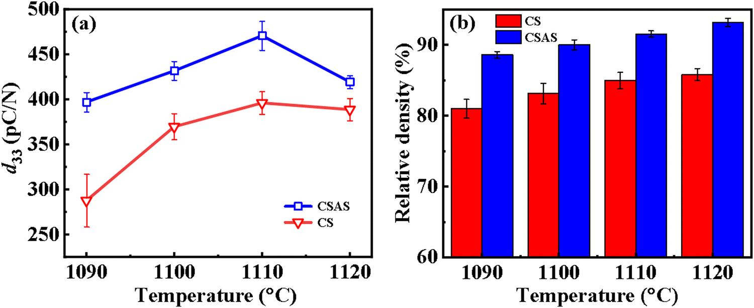 | ||
| Fig. 3 (a) d33 and (b) relative densities of CS and CSAS ceramics with different sintering temperatures. | ||
In order to further analyze the phase structure of the ceramic, the Rietveld structure refinement was performed for the two representative samples, CS-1110 and CSAS-1110, using GSAS, and the results are shown in Fig. 4(a) and (b), respectively. The XRD data were reliably fitted using a hypothetical lattice of rhombohedral (R3m), orthorhombic (Amm2), and tetragonal (P4mm) phases. The phase fractions of the two samples are shown in Table 1. The two compositions are in the coexistence of three phases R–O–T, but their phase ratios are quite different. The Rietveld refinement results show that CSAS-1110 has a reduced R-phase content and an increased T-phase content compared to CS-1110, which is favorable for high piezoelectric performances.36
 | ||
| Fig. 4 (a) and (b) Rietveld refinement of CS-1110 and CSAS-1110 powders. | ||
| Parameters | χ 2 | R p (%) | Space group | Phase proportion (%) | a (Å) | b (Å) | c (Å) | Alpha (°) |
|---|---|---|---|---|---|---|---|---|
| CS-1110 | 3.092 | 6.55 | R3m | 50.8 | 3.9822 | 3.9822 | 3.9822 | 89.982 |
| Amm2 | 36.1 | 3.9718 | 5.6527 | 5.6626 | — | |||
| P4mm | 13.1 | 4.0136 | 4.0136 | 3.9653 | — | |||
| CSAS-1110 | 2.600 | 7.53 | R3m | 26.9 | 3.9899 | 3.9899 | 3.9899 | 89.989 |
| Amm2 | 18.1 | 3.9754 | 5.6431 | 5.6599 | — | |||
| P4mm | 55.0 | 3.9800 | 3.9800 | 4.0042 | — |
Fig. 5 shows the temperature dependence of the dielectric properties of CS-1110 and CSAS-1110 ceramics. As can be seen from the figure, three dielectric anomalies appear, corresponding to the R–O, O–T, and T–C phase transitions of the ceramics. Comparing the two ceramics, the difference of TR–O is very small (around −25 °C) for both ceramics. For TO–T, the CSAS-1110 sample clearly shows a shift towards a lower temperature, which is consistent with the XRD refining results that the CSAS-1110 samples contain a larger proportion of T phase. The εr value of CSAS-1110 ceramics near room temperature at 1 kHz is ∼2 times as that of CS-1110 ceramics, which is supposed to be due to the higher density and larger grain size of CSAS ceramics. It is noteworthy that the CSAS-1110 ceramics maintain a high dielectric constant from room temperature up to 250 °C. Meanwhile, tanδ of the ceramics does not change much with temperature when the temperature is lower than the Curie temperature. When the temperature is higher than the Curie temperature, tanδ of ceramics increases rapidly. This phenomenon can be attributed to the strong migration of defect dipoles in the ceramics at high temperature, which leads to the increase of leakage conductivity and polarization loss of the ceramics.37 Fig. S1 (ESI†) shows the temperature dependence of the dielectric properties of CS-1120 and CSAS-1120 ceramics, which is similar to those of CS-1110 and CSAS-1110 ceramics.
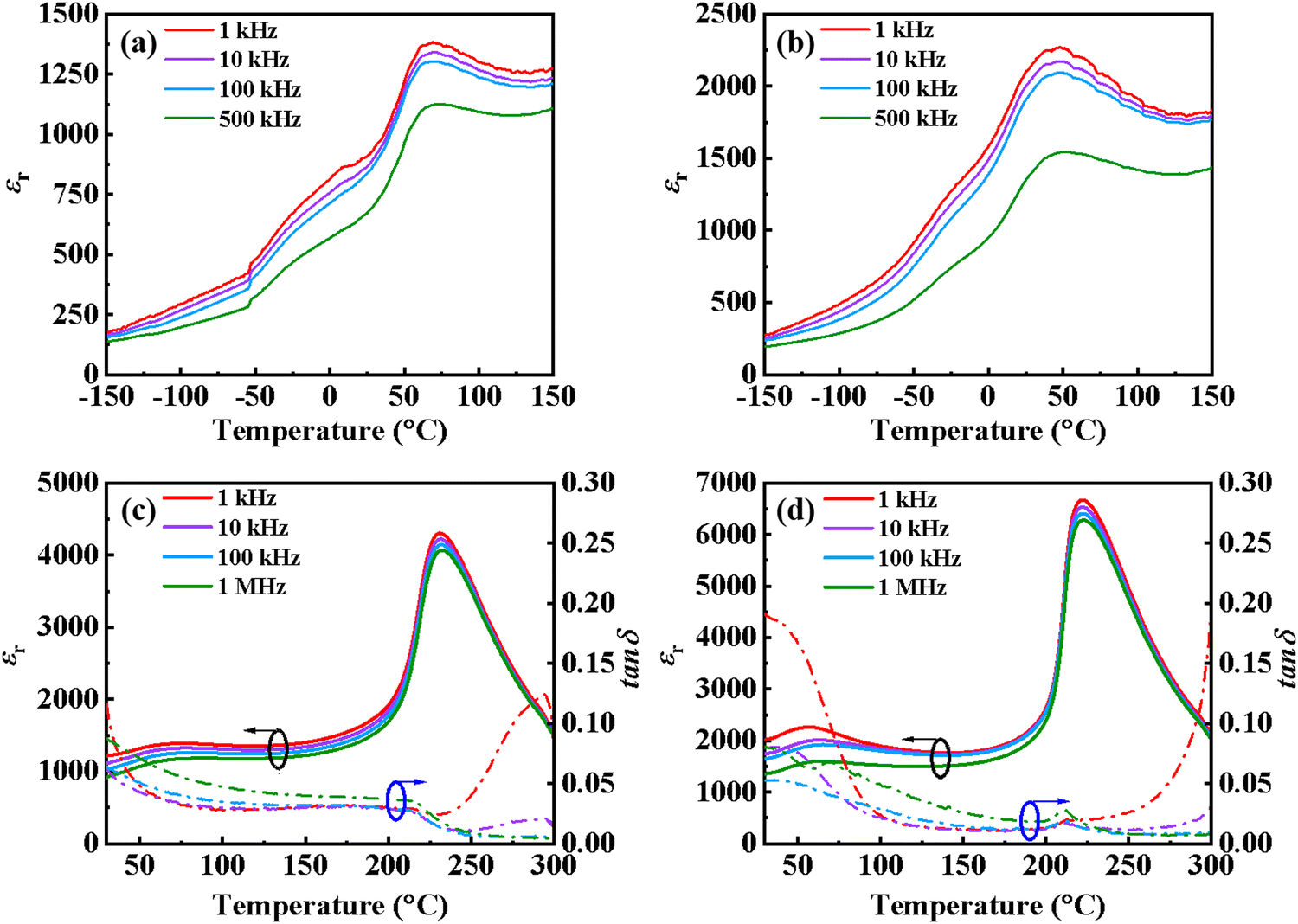 | ||
| Fig. 5 Temperature dependence of the permittivity of (a) CS-1110 and (b) CSAS-1110 ceramics from −150 to 150 °C; temperature dependence of the dielectric loss and permittivity of (c) CS-1110 and (d) CSAS-1110 ceramics from 30 to 300 °C. | ||
Fig. 6(a) shows the P–E hysteresis loops of the of CS-1110 and CSAS ceramics (measurement frequency f = 10 Hz), and all ceramics exhibit typical ferroelectric characteristics. All the P−E hysteresis loops are well saturated, which suggests the low leakage of the prepared ceramics. The CSAS ceramics have stronger ferroelectric properties than the counterpart CS-1110. Pr and EC of CSAS ceramics are shown in Fig. 6(b). Ec does vary little with the sintering temperature. Meanwhile, the Pr value increases from 3.80 to 18.6 μC cm−2 as the temperature increases from 1090 to 1110 °C, and then decreases with the increase of the sintering temperature to 1120 °C. d33 has a similar behavior with Pr. The higher Pr value of CSAS ceramics may be attributed to the larger grain size of CSAS ceramics and weak volatilization of A-site cations, which facilitates the switching of the domain. It is well-known that a high εr·Pr corresponds to a large d33, and the d33 can be calculated using the equation: d33 = 2Qεr·Pr, where Q is the electrostriction coefficient.7,12,13,38Fig. 6(c) shows the d33 and εr·Pr as a function of the sintering temperature for the CSAS ceramics. The variation of d33 and εr·Pr has a similar trend. When the temperature reaches 1110 °C, both d33 and εr·Pr reach their maximum values, indicating that εr·Pr is indeed strongly correlated with d33. Fig. 6(d) presents the electromechanical coupling factor kp and the mechanical quality factor Qm of CSAS ceramics. kp presents the same trend with d33, while Qm is opposite to them. For piezoelectric ceramics, the combination of a high Qm value and a relatively low d33 value is usually considered ‘hard’, whereby the combination of a low Qm value and a relatively high d33 is the feature of ‘soft’ piezoceramics. The low magnitude of Qm implies the relatively ‘soft’ nature of CSAS-1110 ceramics.39
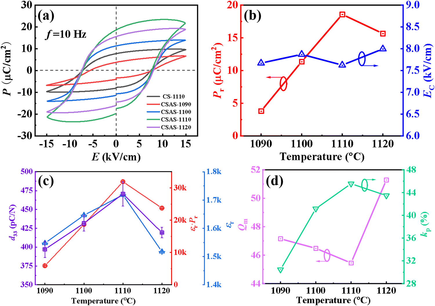 | ||
| Fig. 6 (a) P–E hysteresis loops of CS-1110 and CSAS ceramics. (b) Pr and Ec as a function of sintering temperatures. (c) The variation of d33, εr·Pr and εr with sintering temperatures. (d) kp and Qm of CSAS ceramics with different sintering temperatures. | ||
Maintaining good temperature stability and piezoelectric properties has been a challenge for KNN-based ceramics.40 In fact, although KNN-based ceramics have excellent electrical properties (d33 or  value of >300 pC N−1 or pm V−1), they still lack satisfactory thermal sensitivity. Hence, temperature-dependent unipolar strain curves were measured. As can be seen from Fig. 7(a) and (b), the unipolar strain curves of ceramics are all temperature dependent (30–180 °C). The Suni values of CS-1110 and CSAS-1110 ceramics first increase and then decrease with temperature, reaching a maximum at 60 °C and 40 °C, respectively. The Suni value of the ceramics reaches its maximum close to the phase transition temperature, which coincides with the temperature dependence of the dielectric properties in Fig. 5. For CS-1110 ceramics, Suni(60 °C)/Suni(30 °C) and Suni(180 °C)/Suni(30 °C) are 16% and −30%, respectively, and the total variation of Suni values reaches 46% in the temperature range of 30–180 °C, as shown in Fig. 7(c). Meanwhile, for CSAS-1110 ceramics, Suni(40 °C)/Suni(30 °C) and Suni(180 °C)/Suni(30 °C) are 8% and −32%, respectively, and the total variation of Suni values is 40% in the temperature range of 30–180 °C, as shown in Fig. 7(d). It shows that CSAS-1110 ceramics have superior temperature stability to CS-1110 ceramics. Furthermore, the
  of the CS-1110 ceramic reaches 498 pm V−1 at 60 °C, and this value reaches 598 pm V−1 at 40–60 °C for the CSAS-1110 ceramic. The superior temperature stability and piezoelectricity may be ascribed to the lower content of the O-phase in CSAS-1110 ceramics, which has relatively lower strain values compared to R-phase and T-phase, and thus the decrease in the proportion of the O-phase also contributes to the increase in strain.41 Fig. S2(a) and (b) (ESI†) show the temperature dependence of the unipolar strain for CS-1120 ceramics and CSAS-1120 ceramics, respectively, which is similar to those of CS-1110 and CSAS-1110 ceramics.
 | ||
Fig. 7 Temperature dependent unipolar S–E curves of the ceramics (a) CS-1110 and (b) CSAS-1110 and (c) and (d) the corresponding variation in strain and  for the samples. for the samples. | ||
To investigate the defect of the CS and CSAS ceramics, XPS was carried out for the CS-1110 and CSAS-1110 ceramics. The O 1s spectra of CS-1110 and CSAS-1110 are shown in Fig. 8(a) and (b). Two peaks are identified for both CS-1110 and CSAS-1110. One peak is centered at ∼529 eV, which is considered to correlate with the lattice oxygen. The peak centered at ∼531 eV is related to the adsorbed oxygen.38,42,43 The two peaks can be well fitted by two curves. The ratio of the fitted area of lattice oxygen to adsorbed oxygen (regarded as O2−/VO−) can denote the relative VO− content in the oxide ceramics.44 The ratio of the area under the blue curve to that under the green curve for the two ceramics is 0.085 and 0.215, respectively, which indicates that the CSAS-1110 ceramics contain less oxygen vacancies and less K+/Na+ vacancies, which is consistent with the previous results. Fig. S3(a) and (b) (ESI†) show the O 1s spectra of CS-1120 and CSAS-1120, respectively, and the ratios of the fitted areas of lattice oxygen to adsorbed oxygen for the two samples are 0.042 and 0.046, respectively. This suggests that both samples contain more oxygen vacancies than the counterparts prepared with CS and CSAS at 1110 °C, and that the K+/Na+ volatilization is more drastic when the ceramics are sintered at 1120 °C. It should be noted that XPS peaks of Mn2+ (640.3 eV), Mn3+ (641.1 eV), and Mn4+ (642.9 eV) were not detected because the amount of Mn was below the detection limit of the XPS instrument.
 | ||
| Fig. 8 XPS spectra of O 1s of (a) CS-1110 and (b) CSAS-1110. | ||
The electrical properties of piezoelectric ceramics were closely related to their domain structures. Hence, domain structures including the amplitude and phase of CS-1110 ceramics were observed by PFM. As shown in Fig. 9(a)–(c), both amplitude and phase images have no obvious coupling with the topography image. From the amplitude image in Fig. 9(b), it can be seen that unlike the pure KNN ceramics previously reported in the literature, the CSAS-1110 ceramic displays an irregular and complex domain structure, with small-sized nanodomains in addition to larger block domains (1–2 μm). The size of the domains is proportional to the square root of the energy of the domain wall, and due to lower energy barriers, small-sized nano-domains are more easily reoriented under an external electric field.38,45–47 The heterogeneous domain structure and small-size nano-domains are favorable to the excellent electrical properties of CSAS-1110 ceramics. Fig. 9(d) shows the morphology of the CSAS-1110 sample under a low magnification spherical aberration lens, where the lined area is the domain boundary. Fig. 9(e) shows the HAADF and ABF images of STEM. The difference between Nb and Na/K atoms becomes obvious due to the significant presence of the atomic number Z difference. Two electron diffractograms (Fig. 9(f1) and (f2)) at a low refractive index with the band axis [011] and [100] demonstrate a homogeneous single phase of the ceramics. However, this is actually an averaging effect that does not reflect the local symmetry within the nanodomains. STEM is considered to be a more efficient technique for structural imaging with the ability to interpret the contrast by mass-thickness or Z-contrast.48,49 As shown in Fig. 9(g), we can visually identify the symmetry properties of the three phases (T, O, and R) in the ferroelectrics by observing the spontaneous polarization (PS) (T is [001], O is [110], and R is [111]). For ferroelectric KNN, its spontaneous polarization is formed by the relative shifts of the negative (O2−) and positive (Na+/K+ and Nb5+) ion centers to form an electric dipole. The relative shifts of the Nb5+ cation center with its two nearest O2− neighboring centers (δNb–O) reveal its localized polarization condition, which further reflects its symmetry characteristics.50δNb–O is the method used to calculate the vector relationship between each Nb5+ and its two nearest-neighboring O2− centers of mass. Therefore, we can estimate the direction of the PS vector by observing the δNb–O vector with the direction from net negative charges to positive charges. Fig. 9(h) shows a visual representation of the 2D δNb–O (polarization) vector with the polarization directions of the T, O, and R phases explicitly labeled in it. This indicates that the ceramic is indeed in R–O–T three-phase coexistence, which is consistent with the XRD and dielectric measurement results.
 | ||
| Fig. 9 PFM images of CSAS-1110: (a) topography, (b) amplitude and (c) phase. (d) TEM image of CSAS-1110. (e) The atomically resolved ABF image along [110], with its inset HAADF image. (f1) and (f2) Electron diffraction patterns along [011] and [100]. (g) Schematic projection of the polarization directions for T, O and R phases in the ABO3 unit cell along the [110] zone. (h) The atomically resolved STEM HAADF image along [110], with the δNb–O displacement vector map overlaid on it. The displacement vectors are indicated as arrows, and T, O, and R regions are marked. | ||
4. Conclusions
In summary, KNNS–BNZS–BZ ceramics were prepared by the CSAS method via a low concentration of KMnO4 solution. The effects of the sintering process and sintering temperature on the microstructure and electrical properties of KNN ceramics were investigated. The grain size of the ceramics and the density of the ceramics can be increased, and the volatilization of the A-site elements can be reduced by the CSAS method, thus leading to the change of the proportion of the phase structure of the ceramics, which leads to the ceramics with a high dielectric constant and piezoelectric properties. The CSAS ceramics sintered at 1110 °C exhibit excellent ferroelectric and piezoelectric properties (d33 = 470 pC N−1, εr = 1718, Pr = 18.58 μC cm−2, kp = 0.45, and at 40–60 °C). The present results demonstrate that the CSAS method is promising for the preparation of high-performance KNN-based ceramics.
Data availability
All data supporting the findings of this study are available within the paper and its ESI.†Conflicts of interest
There are no conflicts to declare.Acknowledgements
This investigation was supported by the National Natural Science Foundation of China (12374087), the Key Research and Development Plan of Zhejiang Province (2022C01229), and the Science and Technology Innovation 2025 Major Project of Ningbo City (2022Z211).References
- J. Wu, D. Xiao and J. Zhu, Chem. Rev., 2015, 115, 2559–2595 CrossRef CAS PubMed.
- B. Wu, J. Ma, W. Wu and M. Chen, J. Mater. Chem. C, 2020, 8, 2838–2846 RSC.
- J. Ma, J. Wu, B. Wu and W. Wu, J. Mater. Chem. C, 2020, 8, 9506–9510 RSC.
- Q. Liu, Y. Zhang, J. Gao, Z. Zhou, H. Wang, K. Wang, X. Zhang, L. Li and J.-F. Li, Energy Environ. Sci., 2018, 11, 3531–3539 RSC.
- Y. Wu, P. S. Soon, J. T. Lu, J. Zhou, Y. X. Liu, Z. Guo, K. Wang and W. Gong, EcoMat, 2024, 6, 12450 CrossRef.
- C. Zhao, Y. Huang and J. Wu, InfoMat, 2020, 2, 1163–1190 CrossRef CAS.
- P. Li, Z. Fu, F. Wang, Y. Huan, Z. Zhou, J. Zhai, B. Shen and S. Zhang, Acta Mater., 2020, 199, 542–550 CrossRef CAS.
- B. Wu, C. Zhao, Y. Huang, J. Yin, W. Wu and J. Wu, ACS Appl. Mater. Interfaces, 2020, 12, 25050–25057 CrossRef CAS.
- T. Zheng, Y. Yu, H. Lei, F. Li, S. Zhang, J. Zhu and J. Wu, Adv. Mater., 2022, 34, 2109175 CrossRef CAS.
- Y. Saito, H. Takao, T. Tani, T. Nonoyama, K. Takatori, T. Homma, T. Nagaya and M. Nakamura, Nature, 2004, 432, 84–87 CrossRef CAS.
- P. Li, J. Zhai, B. Shen, S. Zhang, X. Li, F. Zhu and X. Zhang, Adv. Mater., 2018, 30, 1705171 CrossRef PubMed.
- X. Lv, J. Wu and X.-X. Zhang, Chem. Eng. J., 2020, 402, 126215 CrossRef CAS.
- Q. Liu, Y. Zhang, J. Gao, Z. Zhou, D. Yang, K.-Y. Lee, A. Studer, M. Hinterstein, K. Wang, X. Zhang, L. Li and J.-F. Li, Natl. Sci. Rev., 2020, 7, 355–365 CrossRef CAS PubMed.
- X. Lv, J. Zhu, D. Xiao, X.-X. Zhang and J. Wu, Chem. Soc. Rev., 2020, 49, 671–707 RSC.
- J. Xing, H. Chen, L. Jiang, C. Zhao, Z. Tan, Y. Huang, B. Wu, Q. Chen, D. Xiao and J. Zhu, Nano Energy, 2021, 84, 105900 CrossRef CAS.
- X. Lv, N. Zhang, J. Wu and X.-X. Zhang, Acta Mater., 2020, 197, 224–234 CrossRef CAS.
- A. Gadelmawla, U. Eckstein, K. Riess, Y. X. Liu, K. Wang, J. F. Li, Ki Kakimoto, N. H. Khansur and K. G. Webber, J. Am. Ceram. Soc., 2022, 106, 2326–2337 CrossRef.
- C. Zhou, J. Zhang, W. Yao, D. Liu and W. Su, Scr. Mater., 2019, 162, 86–89 CrossRef CAS.
- J. Ma, B. Wu, W. Wu and M. Chen, J. Mater. Sci.: Mater. Electron., 2018, 29, 12323–12329 CrossRef CAS.
- C. Shi, J. Ma, J. Wu, K. Chen and B. Wu, Ceram. Int., 2020, 46, 2798–2804 CrossRef CAS.
- Y. Zhang, B. Wu, M. li, Y. Zhu, X. Liu and D. Ren, J. Wuhan Univ. Nat. Sci. Ed., 2022, 68, 195–202 Search PubMed.
- J. L. Miranda, C. Ribeiro, A. Tkach, A. M. O. R. Senos and P. M. Vilarinho, J. Eur. Ceram. Soc., 2024, 44, 116701 CrossRef CAS.
- H. Guo, J. Guo, A. Baker and C. A. Randall, ACS Appl. Mater. Interfaces, 2016, 8, 20909–20915 CrossRef CAS.
- J. Ma, H. Li, H. Wang, C. Lin, X. Wu, T. Lin, X. Zheng and X. Yu, J. Eur. Ceram. Soc., 2019, 39, 986–993 CrossRef CAS.
- L. Cong, W. Huajing, M. Jianzhang, D. Baoyu, W. Xiao, L. Tengfei, Z. Xinghua and Y. Xing, J. Alloys Compd., 2020, 826, 154249 CrossRef.
- A. Włódarkiewicz, M. E. Costa and P. M. Vilarinho, Mater. Des., 2023, 233, 112169 CrossRef.
- H. Guo, A. Baker, J. Guo, C. A. Randall and D. Johnson, J. Am. Ceram. Soc., 2016, 99, 3489–3507 CrossRef CAS.
- H. Huang, J. Tang and J. Liu, Ceram. Int., 2019, 45, 6753–6758 CrossRef CAS.
- W. Liu and X. Ren, Phys. Rev. Lett., 2009, 103, 257602 CrossRef PubMed.
- D. Damjanovic, Appl. Phys. Lett., 2010, 97, 062906 CrossRef.
- Z. Ma, H. Zheng, L. Zhao, B. Wu, H. Tao, M. Chen and J. Ma, Ceram. Int., 2023, 49, 18629–18637 CrossRef CAS.
- N. Zhang, X. Lv, X.-X. Zhang, J. Lyu, S.-W. Yang and J. Wu, J. Mater. Sci. Technol., 2022, 115, 189–198 CrossRef CAS.
- T. Wang, D. Wang, Y. Liao, Q. Zheng, H. Sun, K. Kwok, N. Jiang, W. Jie, C. Xu and D. Lin, J. Eur. Ceram. Soc., 2018, 38, 4915–4921 CrossRef CAS.
- Z. Cen, Y. Zhen, W. Feng, P. Zhao, L. Chen, X. Wang and L. Li, J. Eur. Ceram. Soc., 2018, 38, 3136–3146 CrossRef CAS.
- J. Guo, R. Floyd, S. Lowum, J.-P. Maria, T. Herisson de Beauvoir, J.-H. Seo and C. A. Randall, Annu. Rev. Mater. Res., 2019, 49, 275–295 CrossRef CAS.
- J. Xing, S. Xie, B. Wu, Z. Tan, L. Jiang, L. Xie, Y. Cheng, J. Wu, D. Xiao and J. Zhu, Scr. Mater., 2020, 177, 186–191 CrossRef CAS.
- X. Huo, F. Wang, T. Zhang, M. Zhang and M. Guo, Ceram. Int., 2023, 49, 15751–15760 CrossRef CAS.
- R. Li, X.-x Sun, X. Lv, T. Zheng and J. Wu, Acta Mater., 2021, 218, 117229 CrossRef CAS.
- F.-Z. Yao, M.-H. Zhang, K. Wang, J.-J. Zhou, F. Chen, B. Xu, F. Li, Y. Shen, Q.-H. Zhang, L. Gu, X.-W. Zhang and J.-F. Li, ACS Appl. Mater. Interfaces, 2018, 10, 37298–37306 CrossRef CAS.
- T. Zheng and J. Wu, Acta Mater., 2020, 182, 1–9 CrossRef CAS.
- L. Jiang, Z. Tan, L. Xie, Y. Li, J. Xing, J. Wu, Q. Chen, D. Xiao and J. Zhu, J. Eur. Ceram. Soc., 2018, 38, 2335–2343 CrossRef CAS.
- Y. Chen, C. Li, X. Ma, Q. Qiang, B. Liu, S. Cao, L. Peng, L. Li and T. Lang, Appl. Surf. Sci., 2020, 506, 144816 CrossRef CAS.
- J. Gong, P. Du, W. Li, G. Yuan, X. Mao and L. Luo, Laser Photonics Rev., 2022, 2200170 CrossRef CAS.
- Y. Zhu, Y. Lv, Y. Xiao, H. Sun, Q. Zhang and X. Hao, J. Lumin., 2019, 215, 116626 CrossRef CAS.
- Y. Cheng, J. Xing, X. Li, L. Xie, Y. Xie, Z. Tan and J. Zhu, J. Am. Ceram. Soc., 2022, 105, 5213–5221 CrossRef CAS.
- Y. Huang, C. Zhao, S. Zhong and J. Wu, Acta Mater., 2021, 209, 116792 CrossRef CAS.
- X. Lv, X.-x Zhang and J. Wu, J. Mater. Chem. A, 2020, 8, 10026–10073 RSC.
- H. Wu, X. Zhao, C. Guan, L. D. Zhao, J. Wu, D. Song, C. Li, J. Wang, K. P. Loh, T. V. Venkatesan and S. J. Pennycook, Adv. Mater., 2018, 30, 1802402 CrossRef.
- T. Zheng, Y. Zhang, Q. Ke, H. Wu, L. W. Heng, D. Xiao, J. Zhu, S. J. Pennycook, K. Yao and J. Wu, Nano Energy, 2020, 70, 10–4559 Search PubMed.
- H. Tao, H. Wu, Y. Liu, Y. Zhang, J. Wu, F. Li, X. Lyu, C. Zhao, D. Xiao, J. Zhu and S. J. Pennycook, J. Am. Chem. Soc., 2019, 141, 13987–13994 CrossRef CAS.
Footnote |
| † Electronic supplementary information (ESI) available. See DOI: https://doi.org/10.1039/d4tc04031g |
| This journal is © The Royal Society of Chemistry 2025 |