
 Open Access Article
 This Open Access Article is licensed under a Creative Commons Attribution-Non Commercial 3.0 Unported Licence
Organic field-effect transistor-based sensors: recent progress, challenges and future outlook
Bibi
Amna
*ab and
Turan
Ozturk
 *bc
*bc
aDepartment of Chemistry, Quaid-i-Azam University, Islamabad 45320, Pakistan. E-mail: bibiamnahussain@gmail.com
bDepartment of chemistry, Istanbul Technical University, 34469 Maslak, Istanbul, Turkey. E-mail: ozturktur@itu.edu.tr
cTUBITAK-UME, Chemistry group of laboratories, PO Box 54, Gebze, Kocaeli 41471, Turkey
First published on 18th March 2025
Abstract
OFET-based sensors consisting of small molecules or polymers as an active layer have garnered significant attention in recent years owing to their high flexibility and sensitivity, low fabrication cost and excellent substrate conformity. Compared to their inorganic counterparts, organic materials hold a rich family of functional moieties that can selectively react or bind with analytes as specific sensing sites. This review highlights recent progress (2018–2024) in the fabrication of OFET-based gas, pressure, temperature, light, pH, humidity, chemical and biological sensors with sensitivities approaching the limits of detection at parts per billion molar concentration. The challenges that are considered a bottleneck in developing sensors that fully meet the requirements for practical applications and the solutions proposed to tackle these challenges have also been included. The optimizations of the OFET devices for sensing activity, including the modification of semiconducting layers, dielectric engineering, and electrodes and their interfaces, are also illustrated. Furthermore, their relationships with sensing parameters, such as sensitivity, selectivity, and response time, as well as the proposed sensing mechanisms are discussed. This review is expected to offer inspiration for the future design of OFET-based sensors with diverse device architectures, as it features the current progress in the design and development of the extended-gate-type OFETs, electrolyte-gated OFETs, polyelectrolyte-gated OFETs, dual-gate OFETs and water-gated OFETs.
1. Introduction
Since the discovery of conducting polymers in the late 1970s, the field of organic electronics has attracted much attention over the last several decades. Compared to their inorganic counterparts, organic semiconductors (OSCs) possess several superior characteristics such as variety in their molecular design, low operating voltage, mechanical flexibility, low cost and capacity for large-scale and low-temperature manufacturing through inkjet printing and solution processing protocols. Tremendous progress has been made in optimizing the chemical, electrical, mechanical, structural and optical properties of various organic materials for device fabrication.1–7 Over the past few decades, organic field-effect transistors (OFETs) have gained increasing attention due to their flexible, low-cost and lightweight features as compared to the traditional inorganic transistors.8–16 Its promising application in various electronic devices, such as radiofrequency identification tags, flexible displays, integrated circuits and chemical/biological sensors, have directed a great deal of research effort towards the improvement of the OFETs with the feasibility of mass production and ease of fabrication.17–261.1. General device design
A typical OFET consists of three electrodes (source, drain, and gate), a gate dielectric and an organic semiconductor layer. A channel current starts flowing through the organic semiconductor layer when a source/drain voltage is applied, which is due to the charge carrier transport. When the gate voltage is applied across the gate dielectric layer, the channel current is modulated by the gate electrode via field-effect doping. In view of the operational principle of OFETs, it is expected that these OFET devices can expand their application range to sensing platforms. The unique current amplification function of transistors makes them an ideal candidate for sensing weak signals, and their multiple output parameters (threshold voltage, source–drain current, subthreshold swing, current on/off ratio) allow them to distinguish complex signals.27–29 Moreover, the organic semiconductor layer is responsible for the sensing action, while every other component of OFET, including the gate electrode, drain/source electrodes and dielectric layer can help in modulating the sensing behavior of the device.30–36 This review primarily deals with the development of organic semiconductor materials for the active channel. There are certain parameters for assessing the sensing performance of a sensor, which are described as follows: (i) selectivity, (ii) responsivity, i.e., the ability of the sensor to respond to input signals, (iii) recovery time, (iv) limit of detection (LOD) and (v) the ability of the sensor to detect changes in the magnitude of the input signal.A sensor based on OFET combines a sensor and amplifier, in which a small change in the channel current produces pronounced variations in electrical properties upon exposure to the chemical analyte; hence, leading to the high-sensitivity, high-throughput sensor having a great potential for miniaturization (Fig. 1). Moreover, as the OFET itself acts as a sensor, the design complexity of the sensor device is significantly reduced, which enables convenient integration of the sensors into other electronics. The number of studies related to OFET-based sensors has rapidly increased irrespective of the typical drawback associated with OSCs, i.e., their low charge carrier mobility, which appears to have little impact on OFET-based sensing applications.
 | ||
| Fig. 1 Schematic of a BGTC OFET-based sensor displaying its operating mechanism. | ||
1.2. Challenges
Irrespective of the significant benefits of OFETs, they also have some intrinsic disadvantages, such as relatively low mobility, inferior operating speed, and low current density compared to inorganic materials.37–39 Moreover, OFETs suffer from poor stability and electrical properties, which result in a slow response (the response time is defined as the time required for the sensor signal to reach from baseline to 90% of its maximum response) and recovery (the recovery time is the time required for the sensor signal to drop from its maximum response to 10% above its baseline level) of the subsequent sensor device.40–42Over the years, despite the improvement in the performance parameters, such as on/off ratio, charge carrier mobility and increased responsiveness of the sensors, the operational instability is still a major problem that restricts commercial applications of OFETs.43–45 In a conventional transistor-based sensor, an analyte must be present at the OSC/environment interface, diffuse into the bulk of OSC, and ultimately reach the OSC/gate-dielectric interface to quantifiably influence the electrical signal.46,47 The arrival of the analyte at the OSC/gate-dielectric interface is vital, as the majority of the electrical charge transport in an OFET occurs at this interface.48 Nevertheless, this type of sensor inevitably suffers from a low sensitivity and a slow response, except the diffusion of the analyte through the semiconductor is immensely efficient. Thus, OFETs require specific structures that enable the analyte to penetrate quickly and adequately into the active channel to achieve high-performance sensing devices.
Over time, a general change in the electrical characteristics of the OFETs is observed with the changed mobility, increased OFF current, shifts of the threshold voltage and increased hysteresis during dual sweep of transfer curves.44,45 This drawback makes OFETs unfit for various practical applications. For instance, when OFETs are employed as sensors, the detection and identification are done by measuring the change in the current. Since the degradation of the device during its functioning also induces a change in the current for constant voltage settings, the signal-to-noise ratio would be uncertain and generally low. Thus, this restricts the use of OFETs as reproducible and reliable sensors. This instability is attributed to many factors, including the interaction with oxygen and moisture, defects in the active layers, bias stress effect and the dielectric polarity.49–51 The instability of the OFET sensors is usually indicated by the degradation of the device performance. The value of the current is decreased and the threshold voltage is increased because the mobile charge carriers become trapped, and thus cannot contribute to the current. The OFETs can recover to the extent that the shift in the threshold voltage is reversible in the case of the bias stress effect; the relaxation time is strongly dependent on the type of semiconductor and the surrounding environment. Additionally, the moisture, oxygen and other gases in air can cause degradation of the device through uncertain mechanisms. Furthermore, the transfer curves measured after a few tests barely shift back spontaneously to the original ones.45 Eliminating the effects of oxygen and moisture, and reducing the defects can reduce the device degradation and improve its operational stability.
Controlling the sensitivity can also be a challenge in designing sensing devices. Although high sensitivity sensors have the advantage of detecting small stimuli, which is important for some applications, it also increases the risk of detecting some interferent weak stimuli. This problem is mostly encountered in pressure sensors. In the case of detecting high pressure, the lower sensitivity can be a better choice. For instance, in monitoring the pulse signals for managing physical health, the weak environmental noise may interfere in the accuracy of sensors. This issue can be managed by the modification of the sensitivity to a suitable (lower) value, in which the weak environmental stimulus cannot produce an output signal. For an efficient sensing device, it is important to balance the sensitivity and selectivity using appropriate shielding, filtering or noise reduction techniques, particularly in environments with vibrations, electrical noise or other unwanted signals.
1.3. Quest of solutions
The OSC-based sensing layer is one of the most crucial factors in fabricating high-performance OFET-based sensors, as the interaction between the target analyte and OSC determines their performance. The chemical structure of OSC and the processing conditions can lead to different states of aggregation of the active layer; thus, the carrier mobility can be artificially optimized. The sensing properties of OFETs are significantly influenced by the interactions between the OSC layer and analyte. These interactions govern the response of the device towards the presence and concentration of the analyte, thus affecting its sensitivity, selectivity and response time (Fig. 2). The intermolecular interactions between the semiconductor molecules and analytes would greatly affect its sensing ability. Therefore, the sensitivity and selectivity of the sensors could be improved through the proper regulation of the molecular structure of OSC in view of the interaction with the detected object. Similarly, dielectric engineering, interface engineering, improved transmission performance, the employment of a hygroscopic insulation layer, modified medium structure, and appropriate blending have made remarkable progress in the development of OFET-based sensors,52–57 as evident from the following examples gathered from recent publications. | ||
| Fig. 2 Factors influencing the interaction between the analyte and OSC layer in the OFET-based sensors. | ||
2. Organic field-effect transistor-based sensors
OFET-based sensors are a promising area of research for developing flexible, low-cost manufacturing, and sensitive detection systems. They are integrated into a variety of applications, including smart devices, environmental sensing and health monitoring. There are various types of OFET-based sensors, depending on the nature of the detected signals (Fig. 3). The main types are discussed in the following sections.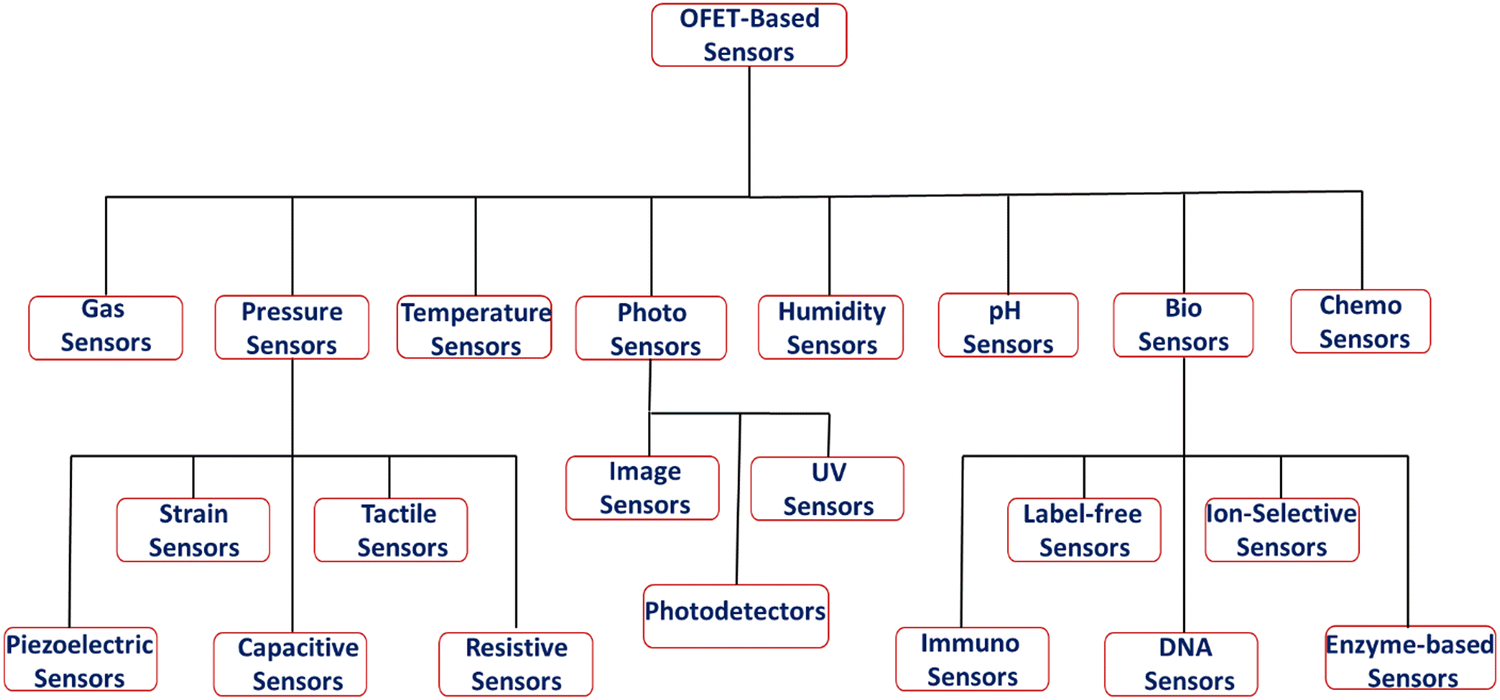 | ||
| Fig. 3 Types of OFET-based sensors discussed in this review. | ||
2.1. Gas sensors
With recent widespread increases in economic activity have come corresponding increases in the combustion of fossil fuels that release toxic gases to the atmosphere.58 NO2, known as one of the dangerous fossil fuel emissions during combustion, has been shown to have negative effects on health, including edema, and nose and throat irritation. Furthermore, NO2 is an important factor in the formation of acid rain and photochemical smog.59 It is abundantly released from industrial sources, and its strong oxidizing properties can critically damage the human respiratory system. Therefore, the accurate and fast detection of NO2 is critical for ensuring workplace safety. HCl is classified as a high-risk gas of Class III hazardous substance. However, it is used in various places, and has a limit of 5 ppm or less. Sarin gas (propan-2-yl methylphosphonofluoridate) is a very toxic gas, which can quickly cause human death at a certain concentration. Dimethyl methylphosphonate (DMMP) is often used as an alternative gas in place of sarin for research purposes, as its chemical structure is similar but its toxicity is much lower than that of sarin.60,61 NH3 is a toxic gas whose detection and quantification have a huge demand in industry and environmental monitoring, as the exposure to high concentrations of NH3 causes severe health issues, including a burning feeling of the throat, respiratory tract and nose, which leads to bronchiolar and alveolar edema and airway destruction, resulting in lung failure. An abnormal concentration of NH3 in exhaled breath is reported to have an interconnection with unhealthy internal organs; for example, the presence of NH3 in exhaled breath greater than 3.2 ppm indicates either kidney failure or renal disease.62–64Organic field-effect transistors (OFET) are especially promising as gas sensors due to their high sensitivity, reusability, good portability, low power consumption, room operating temperature, and cheap production.65,66 A gas sensor based on OFET is gas adsorbed on the surface of the active channel layer. This results in charge movement generated by the surface effect, based on which the degree of field-effect mobility (μFE), on/off current ratio (Ion/off), threshold voltage (Vth) and subthreshold slope (SS) are varied. However, good selectivity and high sensitivity are still challenging issues, hindering their widespread utilization. This has been of great concern for researchers, and constant efforts are being made to develop new sensors with enhanced sensitivity and selectivity.
Song et al. reported a promising strategy for the fabrication of selective organic gas sensors by introducing surface modification.67 Surface modification with a self-assembled monolayer (SAM) was conducted, and a change in the end group of SAM purposefully modulated the device performance and enhanced the interaction with analytes. A series of polymer FET gas sensors were deposited on different SAMs, and exhibited varied sensitivity upon exposure to several gases, including NO2, NH3, SO2 and H2S (Fig. 4). The bare PDQT device demonstrated an obvious response to NH3, but no response was recorded for an oxidative gas. After surface modification, the sensor with a fluorine terminal group, i.e., pentafluorophenylpropyltrichlorosilane (FPPTS), displayed outstanding performance towards NO2 with high responsivity of up to 780% at the saturated region and an LOD as low as 1 ppm. The CH3-terminal SAM using octadecyltrichlorosilane (OTS) and NH2-terminal SAM using 3-aminopropyltrimethoxysilane (APTS) brought moderate sensitivity to gases like NO2 and NH3. Hence, after SAM modification, the performance degradation trend was found to be FPPTS > OTS > APTS. All the devices recovered to the initial state after being exposed to NH3. However, the performance of PDQT/FPPTS could only recover 50% after exposure to NO2 for 30 min. The interaction between reductive gases, like H2S, NH3, and p type OSC resulted in the generation of hole traps and caused the reduction of charge carrier density. In contrast, oxidative NO2 absorption yielded a hole doping effect, leading to enhanced charge carrier density. In the case of oxidative NO2, the exposure of an analyte led to improved electrical performance, including the increase of the threshold voltage and current. Here, the bare devices exhibited a nearly inert response towards NO2, suggesting that the interaction between NO2 and PDQT should be not strong, or the charge transport channel was far from the location of gas absorption.
 | ||
| Fig. 4 (a) Device structure of the OFET with the modified layer (reproduced with permission from ref. 67. Copyright 2021, Elsevier). (b) Molecular structure of the semiconductor polymer PDQT and the molecular structures of the modification materials OTS, APTS and FPPTS. | ||
Wang et al. reported a three-dimensional (3D) copper phthalocyanine (CuPc)-based OFET sensor, obtained by evaporating CuPc on the polyvinyl alcohol parallel nanofiber arrays (PVA PNAs) (Fig. 5).68 The parameters of the two kinds of OFETs are shown in Table 1. This OFET with a 3D structure was conducive to the multi-angle adsorption and desorption of the target gas and active layers. The detection limit of the obtained sensors was lower, and the response and recovery times were also shorter. The response time (Ti) and recovery time (Tii) of different sensors are summarized in Table 2. The minimum detection concentration was reduced by one third, as compared to the single CuPc films and CuPc films with disordered PVA nanofibers sensors. The CuPc/PVA PNAs sensors were successfully used in the real-time monitoring of NO2 at 0.3 ppm concentration. The response and recovery times of the CuPc/PVA PNAs sensors were both 0.02 minutes for 25 ppm NO2. The response and recovery times are 350 and 130 times faster than those of the CuPc sensors having disordered PVA nanofibers, respectively. Table 3 displays a comparison of some previously reported semiconductors employed for fabricating gas sensors of different types with the sensor reported in this article.
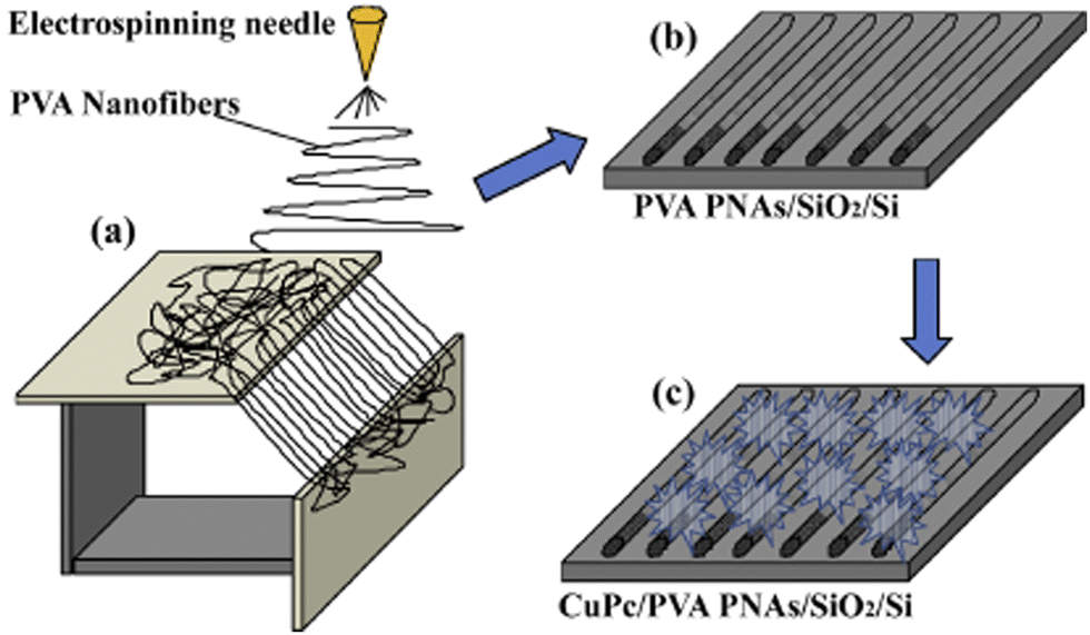 | ||
| Fig. 5 Illustrations of CuPc growth on well-ordered PVA parallel nanofiber arrays (PNAs). (a) PVA PNAs receiving board. (b) PVA PNAs were transferred to SiO2/Si substrates. (c) CuPc was evaporated on PVA PNAs/SiO2/Si (reproduced with permission from ref. 68. Copyright 2021, Elsevier). | ||
| Parameter | CuPc/PVA PNAs | CuPc |
|---|---|---|
| μ (cm2 V−1 s−1) | 8.77 × 10⁻³ | 8.20 × 10⁻³ |
| I on/Ioff | 1.37 × 10³ | 7.52 × 10² |
| SS (V dec−1) | 8.55 | 15.43 |
| C NO2 (ppm) | CuPc/PVA PNAs/SiO2/Si | CuPc/SiO2/Si | ||
|---|---|---|---|---|
| T i (min) | T ii (min) | T i (min) | T ii (min) | |
| 0.3 | 3.07 | 5.88 | — | — |
| 0.5 | 1.19 | 1.21 | — | — |
| 1 | 1.15 | 0.68 | 6.63 | >30 |
| 5 | 1.00 | 0.64 | 4.44 | >30 |
| 10 | 0.10 | 0.32 | 3.32 | 7.10 |
| 15 | 0.05 | 0.05 | 1.81 | 4.21 |
| 20 | 0.03 | 0.04 | 1.52 | 3.55 |
| 25 | 0.02 | 0.02 | 1.31 | 3.32 |
| Materials | Device type | Response definition | Responsivity | Detection limit | Target gas | Response/recovery time | Ref. |
|---|---|---|---|---|---|---|---|
| CuPc/PVA PNAs | Transistor | (Ion − Ioff)/I0 or RNO2/Rair | 952% or 8.16@20 ppm | 0.3 ppm | NO2 | 0.03 min/0.04 min | Wang et al.68 |
| CuPc thin film | Transistor | (Igas − I0)/I0 | 241%@30 ppm | 1 ppm | NO2 | NA | Jiang et al.69 |
| CuPc single nanowires | Transistor | (Igas − I0)/I0 | 764%@20 ppm | 500 ppb | SO2 | 3 min/16 min | Shaymurat et al.70 |
| CuPc/PVA nanofibers | Transistor | (Ion − Ioff)/I0 | 228%@1 ppm | 500 ppb | NO2 | 7 min/4 min | Wang et al.71 |
| CuPc/p-6P/Al2O3/PMMA | Transistor | (Ion − Ioff)/I0 | 1234%@20 ppm | Below 1 ppm | NO2 | 5 min/12 min | Xie et al.72 |
| ZnPc nanofibers | Transistor | (Ion − Ioff)/I0 | 94%@30 ppm | 5 ppm | NO2 | 20 min/20 min | Ji et al.73 |
| VOPc | Resistor | (Igas − I0)/I0 | 1500%@10 ppm | NA | NO2 | 0.5 min/16 min | Wang et al.74 |
| TIPS-pentacene | Transistor | (Ion − Ioff)/I0 | 6300%@5 ppm | 0.3 ppm | NO2 | 3 min/6 min | Wang et al.75 |
| DNTT | Transistor | ΔID/ID,0 | 73%@10 ppm | 10 ppb | NH3 | 1.5 min/— | Lu et al.76 |
| ZnO nanowires | Transistor | (Igas − I0)/I0 | 6200%@5 ppm | 500 ppb | NO2 | —/0.7 min | Ahn et al.77 |
| Electrospun polyaniline | Transistor | (Igas − I0)/I0 | 6000%@700 ppm | 50 ppb | NO2 | 0.8 min/1.2 min | Zhang et al.78 |
| PQT-12 | Transistor | (IDS, NO2 − IDS,air − ΔIreference)/IDS,air | 270%@5 ppm | NA | NO2 | 15 min/— | Li et al.79 |
Yu et al. reported on the preparation of copper phthalocyanine (CuPc)-based gas sensors via solution processable spin coating.80 The spin-coated CuPc films were successfully prepared with a CuPc solution concentration of 45 mg mL−1, 75 mg mL−1 and 105 mg mL−1. The films with a concentration of 75 mg mL−1 were found to have the smallest cracks and the greatest consistency and were the most conducive to achieving high-quality gas sensitivity. The relative responsiveness of the 75 mg mL−1 CuPc films sensors to the NO2 concentration of 20 ppm was found to be 32![[thin space (1/6-em)]](https://www.rsc.org/images/entities/char_2009.gif) 797%. The response rate was found to be 80%, while the response time and recovery time were 4.55 min and 2.50 min, respectively. The LOD was 0.3 ppm, while the sensitivity was reported to be 1492% ppm. The spin-coated CuPc films sensors had better sensitivity and resilience compared to the evaporated CuPc films because of their larger specific surface area, which resulted in the convenient adsorption and desorption of the NO2 gas molecules. The sensors with moderate cracks had the most improved performance, which could be attributed to the poor flow of carriers in the spin-coated CuPc films with several large cracks. The application of the films in gas sensing showed the potential of phthalocyanine-based materials in the field of flexible and 3D printing sensing.
797%. The response rate was found to be 80%, while the response time and recovery time were 4.55 min and 2.50 min, respectively. The LOD was 0.3 ppm, while the sensitivity was reported to be 1492% ppm. The spin-coated CuPc films sensors had better sensitivity and resilience compared to the evaporated CuPc films because of their larger specific surface area, which resulted in the convenient adsorption and desorption of the NO2 gas molecules. The sensors with moderate cracks had the most improved performance, which could be attributed to the poor flow of carriers in the spin-coated CuPc films with several large cracks. The application of the films in gas sensing showed the potential of phthalocyanine-based materials in the field of flexible and 3D printing sensing.
Xie et al. reported on OFET-based NO2 sensors with the alumina/poly(methyl methacrylate) (Al2O3/PMMA) bilayer as the gate dielectrics, and CuPc on the p-6P template layers as the gas sensitive layers.72 The highest NO2 response was displayed by the sensors with 0.8 mol L−1 Al2O3-sol dielectric layer, along with a low baseline drift, fast response/recovery time and stable sensing performance at room temperature (Table 4). The sensitivity was over 129%/ppm and the limit of detection is below 1 ppm (134%) (Tables 5 and 6). The better sensor properties were attributed to the more ordered films on the dielectric layer and better electrical properties with bilayer dielectric devices compared to those with single dielectric devices (Fig. 6). The mobility was found to be improved by above 23 times compared to OFETs with PMMA single dielectric, while the threshold voltage was reduced by 32.47 V. Furthermore, both on–off current radio and saturation current were improved above an order of magnitude for OFET devices containing the Al2O3/PMMA bilayer dielectrics at 0.8 mol L−1 Al2O3-sol.
| C NO2 (ppm) | Responsivity with different Al2O3-sol concentrations (mol L−1) | ||||
|---|---|---|---|---|---|
| 0.2 (%) | 0.4 (%) | 0.6 (%) | 0.8 (%) | 1.0 (%) | |
| 5 | 144 | 212 | 108 | 307 | 23 |
| 10 | 508 | 455 | 162 | 679 | 66 |
| 20 | 1000 | 763 | 313 | 1234 | 83 |
| C NO2 (ppm) | 1 | 3 | 5 | 10 | 15 | 20 |
|---|---|---|---|---|---|---|
| Response time (s) | 271 | 205 | 193 | 167 | 143 | 144 |
| Recovery time (s) | 691 | 933 | 884 | 702 | 816 | 764 |
| Optimal temperature | Responsivity to 6 ppm NO2 | Sensitivity | A low limit of detection | A high limit of detection | Responsivity in stability | Response time | Recovery time |
|---|---|---|---|---|---|---|---|
| To 20 ppm NO2 | |||||||
| RT | 758% | 129%/ppm | 1 ppm (134%) | >35 ppm | 1407% | 144 s | 764 s |
 | ||
| Fig. 6 Conducting channel and NO2 response mechanism based on the (a) bilayer dielectric and (b) single dielectric OFET devices layer (reproduced with permission from ref. 72. Copyright 2019, Elsevier). (c) Molecular structures of the materials. | ||
| Samples | μ FET (cm2 V−1 s−1) | V th (V) | I on/Ioff ratio |
|---|---|---|---|
| Pristine | 0.47 ± 0.036 | −3.1 ± 0.8 | ∼105 |
| Top-NR | 0.48 ± 0.053 | −4.8 ± 1.1 | ∼105 |
| Inter-NR | 0.62 ± 0.082 | −12.9 ± 2.6 | ∼105 |
| Samples | Response rate (s−1) | Recovery rate (s−1) |
|---|---|---|
| Pristine | −0.00084 ± 2.7 × 10⁻⁵ | 0.0011 ± 1.6 × 10⁻⁵ |
| Top-NR | −0.0035 ± 1.4 × 10⁻⁴ | 0.0035 ± 4.5 × 10⁻⁴ |
| Inter-NR | −0.0024 ± 5.0 × 10⁻⁵ | 0.0018 ± 2.7 × 10⁻⁴ |
Darshan et al. reported on an OFET-based room temperature sensor for NH3, employing dinaphtho[2,3-b:2′,3′-f]thieno[3,2-b]thiophene (DNTT), which exhibited a fast response to low concentrations of the analyte down to 100 ppb.82PMMA was used as the gate dielectric material and its hydrophobic surface promoted structured growth of the semiconductor, DNTT, by inducing mass transfer. The sensor performance was improved by controlling the thickness of the semiconductor film. Using a thinner and porous film of DNTT helped in achieving almost double sensitivity of the device towards 1 ppm of NH3, as compared to a thick film of DNTT. Since the intrinsic traps were already present in the organic semiconductor due to thermal vibration and structural defects, the higher number of grain boundaries in a porous film induced increased structural defects, which resulted in a higher density of trap states in the channel. Interaction of the NH3 molecules with DNTT occurred when the devices were exposed to NH3. The field-effect induced hole density produced a net positive charge on the semiconductor channel. The electron pair of NH3 could interact with positively-charged DNTT molecules to form a linkage-type structure (called the base dedoping effect). Holes could be directly immobilized or trapped by these linkages. Since NH3 is a polar molecule, its random absorption could result in disorder and dipole–charge interaction. Such interaction also trapped the holes. The porous film helped in improving this interaction by providing more active sites. Accordingly, the saturation current of the devices displayed an inverse proportionality to the concentration of NH3. When exposed to NH3, the device went into depletion, requiring increased gate voltage to make the channel conductive, which resulted in the increased threshold voltage. These results showed that the trap states at the interface of the semiconductor and dielectric influenced the change in the threshold voltage. The sensing mechanism of the devices with a thick and porous semiconductor layer is shown in Fig. 7. The optimized sensor exhibited a fast response within less than 1 min, with a recovery to 90% of the initial state within 2 min with excellent sensitivity to the NH3 concentration down to 100 parts per billion.
 | ||
| Fig. 7 Illustration of the analyte-semiconductor interaction: (a) device 1, before the exposure; (b) device 1 with the thicker DNTT film, after the exposure; (c) device 2 with the porous DNTT film, after the exposure layer (reproduced with permission from ref. 82. Copyright 2021, Elsevier); (d) semiconductor, Dinaphtho[2,3-b:2′,3′-f]thieno[3,2-b]thiophene (DNTT). | ||
Oh et al. employed the solvatochromic dye (Nile red, NR) with twisted intramolecular charge-transfer (TICT) behavior, depending on the polarity of the surrounding molecules, as an auxiliary NR sensing medium (aNR-SM).81 Intra-charge transfers from the donor diethylamine group to the ketone group occurred in the NR molecule when the polar molecule approached, causing the twisting of the donor functional group and thereby increasing its dipole moment. This characteristic was exploited for detecting NH3 by applying NR as an auxiliary sensing medium to the OFET. The Top-NR case, in which aNR-SM covered only the top of the organic semiconductor layer, was reported to display the best gas sensing performance. Furthermore, its response and recovery rates were improved by 46% and 94%, respectively, as compared to the pristine case. A sensitivity of 0.87 ± 0.045 ppm−1% was measured, having almost perfect linearity (0.999) over the range of the measured NH3 concentrations, which resulted in solving the saturation problem in the sensing characteristics of the OFET-based gas sensor. Schematic diagrams exhibiting the structural comparison of the OFET-based gas sensors are shown in the Fig. 8. The pristine case represents a basic DNTT OFET, which was fabricated with a BGTC structure without an aNR-SM. The Top-NR and Inter-NR cases were classified according to the deposited regions, where the aNR-SM was positioned. The aNR-SM is covered only on the DNTT OSC layer in the Top-NR case. Meanwhile, aNR-SM is located not only on the OSC surface, but also in the OSC/electrode interface region in the Inter-NR case, by depositing the NR after the OSC film formation. In the Inter-NR case, a large negative shift in Vth appears since it is more affected by the presence of the aNR-SM layer during the charge injection. In addition, improvements in the μFET are considered to be due to physical doping, as the NR molecules are deposited on the DNTT active layer. The Top-NR and Inter-NR cases show a greater decrease in the ID level with increasing NH3 concentration than in the pristine case. The amplification of the sensing signals of the Top-NR and Inter-NR cases could be attributed to the increase in the dipole moment of the aNR-SM formed on the OSC surface by exposure to ambient NH3 gas, and the increase in the trapping of NH3 molecules due to the interaction between the NR and NH3 molecules (Tables 7 and 8).
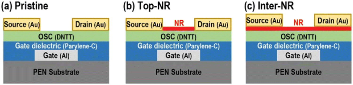 | ||
| Fig. 8 Schematics for three types of DNTT FET devices: (a) pristine, (b) Top-NR, and (c) Inter-NR cases (reproduced with permission from ref. 81. Copyright 2021, ACS). | ||
Kang et al. reported on three conjugated polymers with the same conjugated framework, but different side chains having different branch points and polarities for fabricating sensor for the detection of NO2.835-PDBF and 2-PDBF with alkyl side chains exhibited excellent carrier mobility, whereas 2EO-PDBF with glycol side chains showed moderate carrier mobility for each conjugated polymer. The response to NO2 displayed an opposite tendency to the charge carrier mobility (Fig. 9). The discriminated electrical properties of the polymers were attributed to the differences in the nano-dimensional morphology and crystallinity. 5-PDBF with partly linear side chains showed a more tightly inter-packed molecular configuration between the conjugated backbones. Thus, its film had a large crystallite with a low number of defects. However, the gas-sensing performance of 5-PDBF was inferior to that of 2EO-PDBF. In particular, the 2EO-PDBF sensor displayed fast and reversible NO2 detection with an LOD of 0.24 ppb. It also showed excellent selectivity towards NH3, SO2 and CO2. The glycol side chain played a crucial role in enhancing the adsorption and diffusion of NO2 as it provided favorable conditions, such as NO2-affinitive characteristics, loosely packed molecular arrangement, and energetically degenerated NO2-binding sites. The obtained results suggested that enhancing the affinity with target analytes is an efficient approach to ameliorate the sensitivity and selectivity of conjugated polymer-based FET gas sensors.
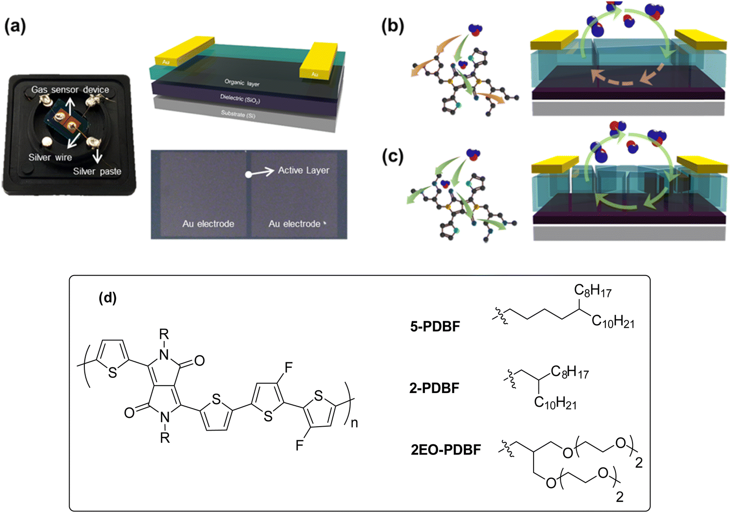 | ||
| Fig. 9 (a) Actual gas sensor image (left), device schematic (right/top), and OM image of the device (right/bottom). Schematic showing the apparent difference in the sensitivity and the saturation/recovery characteristics for (b) 2-PDBF or 5-PDBF and (c) 2EO-PDBF FET sensors (reproduced with permission from ref. 83. Copyright 2021, ACS). (d) Chemical structures of the conjugated polymers, 2-PDBF, 5-PDBF and 2EO-PDBF FET. | ||
Sizov et al. reported on a new design of reusable gas sensors based on Langmuir−Schaefer monolayer OFETs (LS OFETs) fabricated from the organosilicon derivative of [1]benzothieno[3,2-b][1]-benzothiophene for detecting NH3 and H2S at low concentrations down to tens of ppb (Fig. 10c).84 The Langmuir–Schaefer technique was employed for the OSC monolayer deposition, which enabled the formation of a 2D-crystalline monolayer film with high device yield and excellent reproducibility (Fig. 10a). The chemically inert nature of the organosilicon semiconducting material allowed for OFET manufacturing under ambient conditions in the presence of air and water vapors. Selectivity was achieved using the multiparametric detection principle, where specific variations of the device parameters were correlated with the target gas. The sensing mechanisms for NH3 and H2S molecules by the LS OFETs were significantly different (Fig. 10b). In the case of NH3, the molecules interacted with the surface of the OSC film due to the strong electron properties of NH3. The electron pair from nitrogen easily interacted with the positively charged holes, which were ejected by the field effect into the LS film. In the case of H2S, the molecules had only weak electron-donor properties and did not significantly trap holes on the OSC surface. However, they diffused into the monolayer OSC and modulated its conductivity through the variation of the potential barrier between the grains. The differences in the sensing mechanisms for these two gases led to different LS OFET characteristics’ responses, enabling a multiparametric detection of toxic gases.
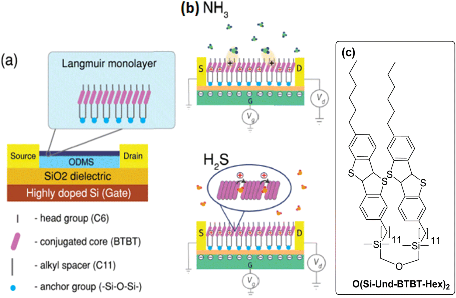 | ||
| Fig. 10 (a) LS OFET device architecture. (b) Suggested mechanisms of NH3 and H2S (reproduced with permission from ref. 84. Copyright 2018, ACS). (c) Chemical structure of the organosilicon dimer O(Si-Und-BTBT-Hex)2 in the closed conformation. | ||
Anisimov et al. reported on the microbiological verification of a novel approach for monitoring the quality of food and detecting spoilage using an electronic nose based on OFETs.85 The newly designed compact device was able to sense gases related to spoiled food as early as at the 4 × 10⁴ CFU per g bacteria count level, which is below the safe consumption threshold by 2 orders of magnitude. A cross-sensitive sensor array of monolayer OFETs based on the siloxane-containing derivative of [1]benzothieno-[3,2-b][1]-benzothiophene OSC (D2-Und-BTBT-Hex) was designed. Different metalloporphyrin receptor layers on a single substrate were used for tuning the sensor response selectivity (Fig. 11). Initially, a set of metalloporphyrin receptors (Cu–, TiO– and Zn–TPP) was considered for providing discriminative ability between four gases: H2S, NO2, ethyl mercaptan (Et-SH), and NH3. At the same time, various sulfur-containing (such as dimethyl sulfide) and amine-containing compounds (such as dimethylamine, methylamine and cadaverine) with higher or comparable molecular weights, compared to the gases mentioned above, were reported to be markers of protein decomposition, and thus can be used for detecting food spoilage. This means that the same sensors can be applied to detect them. The sensitivities toward water vapors and alcohols were found to be at least 3 orders of magnitude lower than NO2 due to the presence of long hydrophobic alkyl chains in the OSC molecules employed. This enabled sensing of the target analytes in the presence of many volatile organic compounds, water vapors and CO2 in the background.
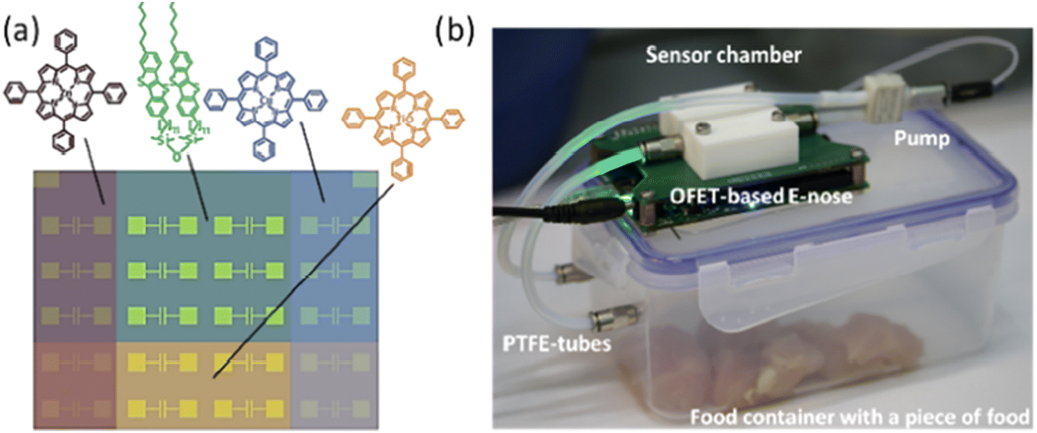 | ||
| Fig. 11 (a) Schematic representation of the sensor array with 20 monolayer OFETs, where different colors represent the areas covered by various receptor layers (TiO–, Cu–, and Zn–TPP) and nonmodified sensors in the substrate center with the bare D2-Und-BTBT-Hex organic semiconductor. (b) Scheme of the experiments with a food container connected to the sensor chamber via a micropump (reproduced with permission from ref. 85. Copyright 2021, Springer Nature). | ||
Wagner et al. reported the improved vapor responses and altered response ratios of thiophene-based copolymers containing oxygenated side chains (linear polyethylene glycol, crown ether and CH2OH) including the poly(3-hydroxymethylthiophene) (PTOH) and other newly synthesized polymers (Fig. 12).86 Hydroxymethyl-bearing copolymers displayed higher mobility than poly(3-hexylthiophene) (P3HT). The response of the thiophene-based polymers was increased towards NH3, NO2 and acetone by the incorporation of different oxygen-bearing functionalities. The polyether side chain enhanced the NO2 response sensitivity of the copolymers of both P3HT and PTOH, but the sensitivity towards gas analytes was found to be more prominent for glycol-based functionalities rather than the crown ethers. PTOH was very sensitive to NO2, and the response likely included a contribution from conductive protons on the OH group. The lack of correlation among the rank-ordered gas sensitivities imparted by each functional group was found to be useful for designing a selective sensor array. A high classification accuracy for all the polymer responses to NO2 and acetone vapors was reported, both of which gave increased device currents, but with response ratios different enough to allow for highly classifying discriminant functions to be derived.
 | ||
| Fig. 12 Chemical structures of the thiophene-based homo- and co-polymers. | ||
Fan et al. reported on a subparts per million-sensitive NO2 sensing circuit with improved humid air stability by UV-ozone treatment on a poly(bisdodecylquaterthiophene) (PQT-12)/polystyrene (PS)blend film.87 The circuit comprised of a pair of OFETs in series, one OFET with and one without this treatment. Schematic structure and the diagram of the OFET-based circuit is shown in the Fig. 13. OFETs consisting of a UV-ozone treated PQT-12/PS blend film was defined as device A, while the untreated OFETs were defined as device B. UV-ozone treatment was expected to induce functional groups on the surface of the PS film and the generated functional groups hold the ability to absorb the NO2 analyte, which was mandatory for achieving ultrasensitive sensors. In comparison to the previous OFET sensors, the readout was obtained from the voltage Vout at a point between the OFETs. The circuit displayed a low detection limit (200 ppb) towards NO2, and greatly reduced the voltage drift in the humid environment compared to the current drift of the circuit or the individual OFETs because of the balance of conductance drifts on either side of the readout point, which differed from the existing OFET-based sensors. The sensitivity of the circuit approached 25% and 400% for NO2 concentrations of 200 ppb and 20 ppm, respectively, by using Vout as the detection parameter (The U.S. government exposure limits are approximately 200 ppb and 1 ppm for long- and short-term exposure, respectively). Furthermore, the Vout is substantial enough to be easily measured by a voltmeter, which could remove the need for complex equipment (semiconductor analyzer system) for the sensing test.
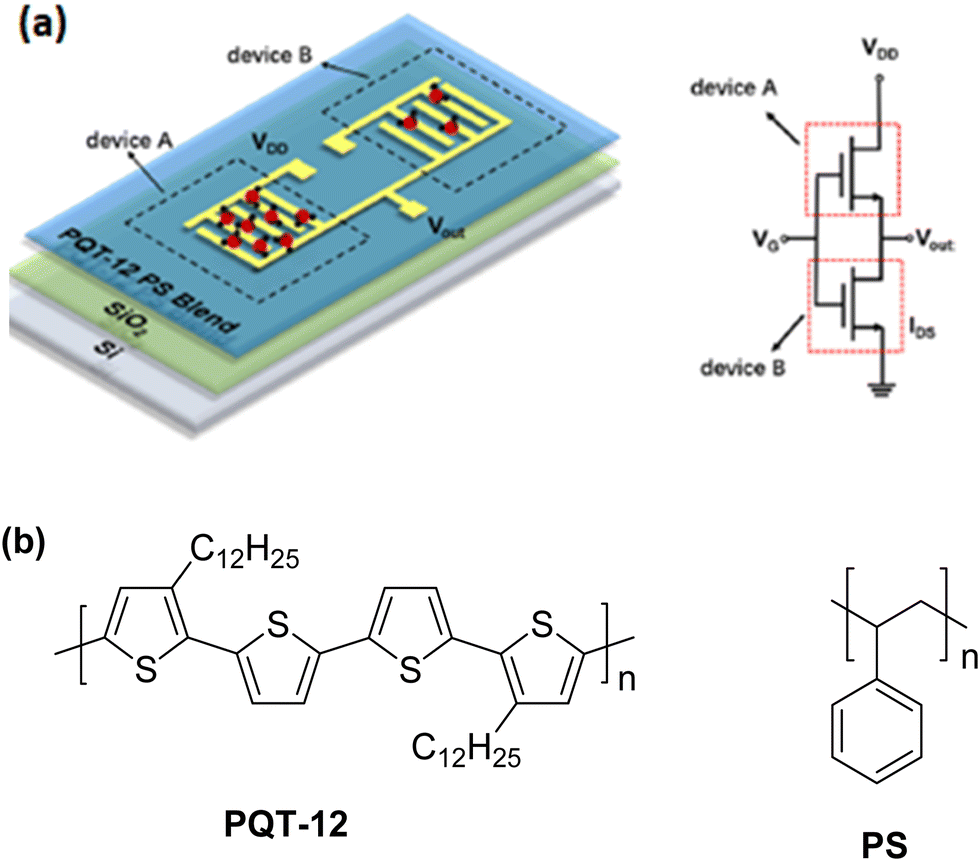 | ||
| Fig. 13 (a) Structure and diagram of the OFET-based circuit (reproduced with permission from ref. 87. Copyright 2019, ACS) and (b) the chemical structure of PQT-12 and PS. | ||
Mukhopadhyaya et al. reported a series of five diketopyrrolopyrrole-fluorene-based polymer semiconductors via modification of the polymer backbone to achieve and rationalize enhancements in gas sensitivities and electronic stability in air (Fig. 14).88 OFETs were fabricated in the BGTC configuration as sensing devices. P6 showed a high hole mobility of 0.12 ± 0.02 cm2 V−1 s−1, while the other polymers exhibited low hole mobilities. The Vth values of the polymers, containing the fluorene spacer, are higher than those of P6 and P7. These polymers were used as active layers to detect NO2 in concentrations as low as 0.5 ppm. The sensitivities displayed a bias voltage-dependent behavior. The proportional on-current change of OFETs using a dithienyl DPP−fluorene polymer reached ∼614% for an exposure to 20 ppm of NO2 for five minutes, testing at a bias voltage of −33 V. Sensitivities with the VG set to (Vth-40) are tabulated in Tables 9 and 10 to show the trends in the NO2 and NH3 sensitivities. The less electron-donating fluorene main-chain subunit led to increased signal/drift compared to the thiophene and carbazole moieties. The introduction of the fluorene unit in the DPP backbone reduced the ease of the backbone oxidation and induced traps in the thin films. The gas-absorbing properties of these materials were governed by the combination of thin-film morphology and oxidation potentials. In this class of OSCs, the ratio of responses on exposure to NO2 and NH3 compared to drifts while taking the device through repeated gate voltage sweeps is the highest for two polymers incorporating electron-donating linkers that connect the diketopyrrolopyrrole and thiophene units in the backbone. A much larger response to NO2 compared to NH3 indicated increased susceptibility to oxidization compared to the reducing gases. Furthermore, the capability of the oxidizing gases to induce additional charge density has a more dramatic electronic effect than when traps are created by the reducing gases.
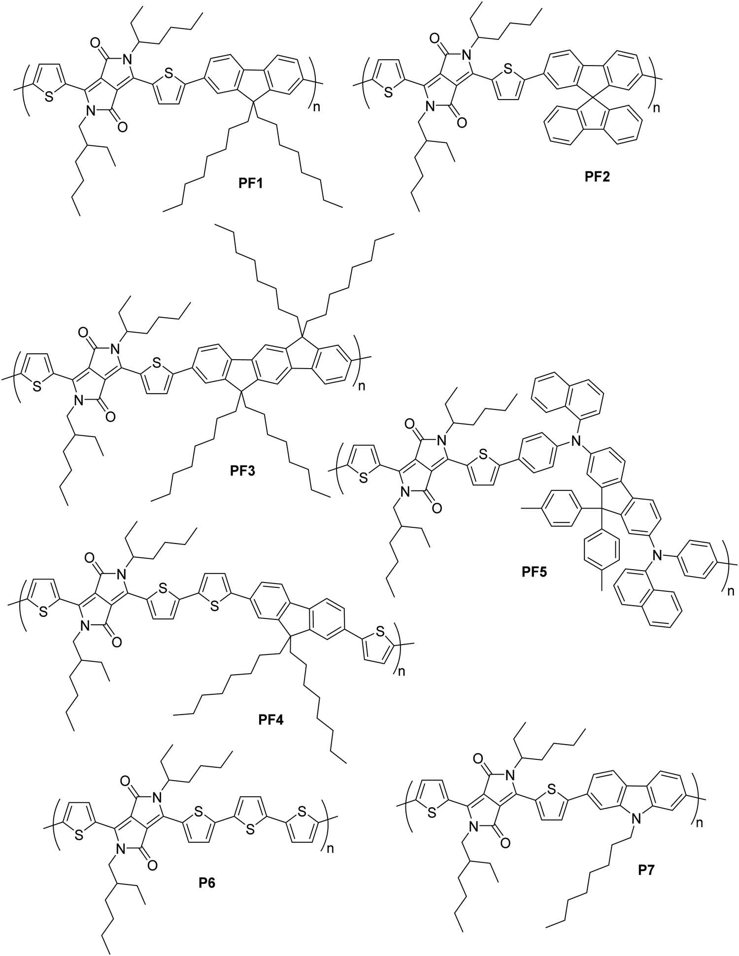 | ||
| Fig. 14 Chemical structures of polymers PF1–PF4 and reference polymers P6 and P7. | ||
| Polymer | Sensitivity (%) | Sensitivity (%) | Sensitivity (%) | Sensitivity (%) | D a | D | D | D |
|---|---|---|---|---|---|---|---|---|
| 1 ppm | 5 ppm | 10 ppm | 20 ppm | 1 ppm | 5 ppm | 10 ppm | 20 ppm | |
|
D
a
= response-to-stability ratio parameter, calculated as D = (ΔI/I)exposure, Δt/(ΔI/I)withoutexposure,Δt where Δt is the time interval of exposure of the sensing device to the vapors for a particular concentration of the gas. ppm = parts per million (one part of the substance per one million parts of the solution). |
||||||||
| PF1 | 27 ± 0.7 | 115 ± 6 | 165 ± 4 | 272 ± 5 | 1 ± 1 | 4 ± 1 | 5 ± 2 | 9 ± 2 |
| PF2 | 34 ± 4 | 79.2 ± 5 | 101 ± 9 | 122 ± 15 | 2 ± 6 | 4 ± 4 | 5 ± 2 | 6 ± 2 |
| PF3 | 10 ± 9 | 152 ± 13 | 210 ± 17 | 355 ± 4 | 2 ± 3 | 3 ± 1 | 5 ± 1 | 8 ± 2 |
| PF4 | 20 ± 12 | 93 ± 6 | 179 ± 1 | 329 ± 20 | 2 ± 1 | 10 ± 1 | 19 ± 2 | 35 ± 1 |
| PF5 | 30 ± 17 | 81 ± 27 | 150 ± 15 | 334 ± 9 | 8 ± 6 | 21 ± 1 | 39 ± 2 | 86 ± 2 |
| P6 | 157 ± 12 | 258 ± 15 | 571 ± 11 | 614 ± 22 | 12 ± 6 | 19 ± 1 | 43 ± 1 | 46 ± 1 |
| P7 | 10 ± 9 | 53 ± 18 | 99 ± 25 | 192 ± 12 | 1 ± 1 | 4 ± 2 | 7 ± 1 | 13 ± 1 |
| Polymer | Sensitivity (%) | Sensitivity (%) | Sensitivity (%) | Sensitivity (%) | D | D | D | D |
|---|---|---|---|---|---|---|---|---|
| 1 ppm | 5 ppm | 10 ppm | 20 ppm | 1 ppm | 5 ppm | 10 ppm | 20 ppm | |
| PF1 | 9 ± 2 | 18 ± 4 | 27 ± 5 | 37 ± 6 | 1 ± 1 | 2 ± 1 | 3 ± 1 | 3 ± 1 |
| PF2 | 14 ± 12 | 25 ± 4 | 34 ± 8 | 43 ± 11 | 1 ± 1 | 2 ± 1 | 3 ± 1 | 4 ± 1 |
| PF3 | 22 ± 10 | 27 ± 4 | 33 ± 9 | 39 ± 5 | 1 ± 1 | 2 ± 1 | 2 ± 2 | 2 ± 1 |
| PF4 | 6 ± 1 | 9 ± 1 | 14 ± 3 | 20 ± 2 | 2 ± 1 | 5 ± 1 | 7 ± 1 | 9 ± 2 |
| PF5 | 34 ± 9 | 41 ± 12 | 59 ± 9 | 68 ± 3 | 9 ± 1 | 11 ± 2 | 14 ± 1 | 16 ± 1 |
| P6 | 16 ± 4 | 24 ± 6 | 27 ± 7 | 36 ± 8 | 1 ± 2 | 2 ± 2 | 3 ± 1 | 5 ± 1 |
| P7 | 10 ± 3 | 13 ± 6 | 21 ± 2 | 33 ± 4 | 3 ± 1 | 4 ± 1 | 5 ± 1 | 7 ± 2 |
While the traps are typically regarded as an obstacle to achieving high-performing semiconductor devices, they can also be exploited towards sensing as analytes modulate the trap density of states (DOS). The generation or passivation of charge carrier traps can thus be the predominant mechanism of sensing by polymers in OFETs.
Mukhopadhyaya et al. established the major role of traps in the vapor-sensing mechanism of a series of five air-stabilized p-channel conjugated polymers (Fig. 15).89 The energetic distribution of the charge traps and the capability of creating them in the polymers as a function of backbone structure was investigated. A polymer with a twisted backbone was observed to be capable of creating an energetically broad trap distribution, while the one with a high degree of solid-state order showed a tendency to form an energetically narrow trap distribution and a fast passivation of traps on exposure to air. The stability and energetic distribution of traps when polymers are subjected to bias stress was related to the electronic structure, as well as solid-state packing. The highest hole mobility of 0.12 ± 0.02 cm2 V−1 s−1 was shown by P6, and PF3 exhibited a p-channel mobility of ∼(1.2 × 10⁻³) cm2 V−1 s−1 ± (7 × 10⁻⁴) cm2 V−1 s−1. Meanwhile, the films of the other four polymers displayed much lower hole mobilities of ∼2.0 × 10⁻⁴ cm2 V−1 s−1. This study revealed that PF2 was capable of creating an energetically broad distribution of traps, while P6 was found to create a narrow distribution of traps. A larger, stable shift in Vth during the static biasing process indicated the presence of deep traps or localized states within the grain boundaries; the density of which was higher in PF2. The ability of the analyte vapors to passivate and create traps, and release carriers was monitored by the recovery time after bias stress in the presence and absence of the vapors, illustrating the role of the traps in the vapor response under different conditions. The recovery from bias stress under an ambient atmosphere is the fastest for P6, while PF2 shows the lowest tendency to refill the created traps when exposed to air for similar time scales as the NO2 exposure, which accelerated the recovery. The ability of NO2 and NH3 for filling/creating traps was further evaluated. Polymers retained their NO2 sensitivity, both post NO2-aided recovery and air-aided recovery, at a bias stress condition of VG = VD = −80 V. The ability of NH3 for creating traps was verified by erasing the traps from the OFET sensors. This was achieved by charging with the aid of a positive gate voltage, leading to an increased NH3 response compared to the air controls.
 | ||
| Fig. 15 Chemical structures of diketopyrrolopyrrole-fluorene and diketopyrrolopyrrole-bithiophene-based polymers. | ||
Ahn et al. studied the effect of side chains on the electrical properties of conjugated polymers by designing two different conjugated polymers containing alkyl and ethylene glycol (EG) groups as side chains on the same conjugated backbone with an electron donor–acceptor (D–A) type chain configuration.90 These polymers displayed completely different electrical properties, although they exhibited similar smooth morphologies and weak crystalline chain assemblies in the film state. PTQ-T with alkyl side chains showed typical p-type semiconducting characteristics, whereas electrical conducting behavior was displayed by PTQ-TEG with EG-based side chains. Both polymers have radical species due to their strong D–A type conjugated structure (Fig. 16). The oxygen atoms of the EG-based side chains, additionally intercalating with the conjugated backbone, increased the carrier density, and ultimately generated the conductor-like properties of PTQ-TEG. A higher NO2 sensitivity with a faster recovery rate was shown by PTQ-TEG compared to PTQ-T. When PTQ-T and PTQ-TEG were applied to FET and resistive-type sensors, the flexible EG-based side chains increased the free volume of the conjugated polymer chains, as well as the affinity with polar NO2 molecules. This facilitated NO2 diffusion in and out of the PTQ-TEG film, resulting in its better sensitivity towards NO2 compared to PTQ-T. It was also confirmed that the EG-based side chains in PTQ-TEG barely impaired the detection selectivity for other common gases, such as CO2, NH3 and SO2, with non-polar neutral, electron-donating and electron-withdrawing characteristics, respectively. The detection sensitivities were found to be in the following order: NO2 (6.9% ppm−1), SO2 (0.03%/ppm), NH3 (0.05%/ppm) and CO2 (0.19%/ppm).
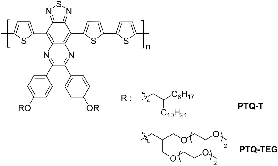 | ||
| Fig. 16 Chemical structures of the conjugated polymers. | ||
Yang et al. employed two semiconducting polymers, poly(3-hexylthiophene-2,5-diyl) (P3HT) and poly(9-vinylcarbazole) (PVK), for the fabrication of OFET consisting of a polymer bulk heterojunction.91 An in-depth investigation of the underlying sensing mechanism was conducted by exploiting the atmosphere influence on device characteristics and NO2-sensing performance of the OFETs. Initially, the individual device characteristics and sensing performance under certain concentrations of NO2 were investigated by using N2 and dry air as carrier gases. O2 was found to have a greater effect on the electrical performance compared to other atmospheric components, which was different from the previous report of a neat P3HT-based device. Specifically, the response of the drain current under N2 was more than two times higher than that under dry air at the high gate voltage, and a 2-fold enhancement was observed in the mobility. In contrast, at a low gate voltage, i.e., 0 V under dry air, the response was 2-fold greater than under N2. The underlying sensing mechanism of these gas sensors was investigated with various P3HT fractions under different operating environments. The gas sensor with 50% P3HT displayed high sensitivity to NO2 under dry air. The highest current sensitivity was ∼12381% for 15 ppm (∼700% for 600 ppb) which was more than 30 times greater than that of pure P3HT. These sensors clearly distinguished NO2 as low as 300 ppb.
Sagdullina et al. reported on the synthesis of N,N-diperfluoroheptyl naphthalene diimide (FNDI), and successfully used it as a promising n-type semiconductor material for OFETs and OFET-based amine-selective gas sensors.92 Benzocyclobutenesilicon resin (BCB) was applied as a thermally stable passivation coating in these devices (Fig. 17). These sensors demonstrated a strong response towards NH3 and amines, along with a high operational stability and good reproducibility of their electrical and sensor characteristics. They were characterized by a low analyte detection threshold estimated to be below 1 ppm and a high speed (response time ≤10 seconds). Moreover, the fabricated sensors displayed good group selectivity with respect to ammonia and aliphatic amine-type analytes. The device sensitivity increased while going from NH3 to trimethylamine, and then to dimethylamine. Meanwhile, no pronounced selectivity was found within the group of amines and NH3 due to the single mechanism of interaction between these analytes and FNDI. This fact imposed restrictions on the use of these sensors for the detection of individual amine-type analytes or discriminating them in a gas mixture. The newly fabricated sensors were insensitive with respect to other types of analytes, which lacked an amine-type structure. Such group selectivity could be useful for a number of applications. The analytes detected by the FNDI-based sensors could be important markers for expressing the diagnostics of diseases, such as chronic liver diseases (ammonia, dimethylamine and trimethylamine), acute and chronic radiation syndromes (ammonia), renal failure (ammonia, trimethylamine), and pancreatic diseases, e.g., benign and malignant tumors (trimethylamine). Additionally, the selectivity of these sensors with respect to amines could be useful for monitoring food quality and controlling air pollutions.
 | ||
| Fig. 17 (a) General layout of the OFET (reproduced with permission from ref. 92. Copyright 2020, Elsevier); (b) structure of the semiconductor FNDI and the dielectric material BCB. | ||
Huo et al. explored the influence of intermolecular interactions on the performance of the OFET-based sensors by employing a series of organic semiconductors based on thienylene-vinylene-thienylene (TVT) derivatives, such as (E)-1,2-bis(5-(naphthalen-2-yl)thiophen-yl)ethene (TVT-NA), (E)-1,2-bis(5-(benzofuran-2-yl)thiophen-2-yl)ethene (TVT-BF) and (E)-1,2-bis(5-(benzo[b]thiophen-yl)thiophen-2-yl)ethene (TVT-BT) (Fig. 15b).93 OFETs based on the TVT derivatives displayed the highest mobility up to 0.69 cm2 V−1 s−1 for TVT-NA. A gas sensor based on the OFET containing TVT-BF as the OSC layer demonstrated good sensitivity and selectivity for the detection of NH3 gas (Fig. 18a). The response and recovery times of the three TVT sensors were measured when taking them in and out of the gas chamber with the concentration of 10 ppm NH3 vapor, and the drain current were measured at VGS = −30 V. Both the response and recovery times were within twenty to thirty seconds. The TVT-BF sensor was exposed to 1 ppm NH3 vapor for four times. Its performance had no obvious change, which indicated its good stability. Significantly different sensing capabilities were displayed by the TVT derivatives for NH3, and the experimental results were consistent with the difference of intermolecular interaction force between NH3 and TVT derivatives, revealed by the simulation calculation (Fig. 19). The binding energies between NH3 and TVT-BT, TVT-NA and TVT-BF were found to be −0.126 eV, −0.066 eV and −0.168 eV, respectively. Different types of noncovalent interactions, such as van der Waals forces, hydrogen bonding and steric crowding were taken into account and the TVT-BF displayed much stronger interactions than that of TVT-BT and TVT-NA. This could be attributed to the stronger hydrogen bond formed between the oxygen atom of furan and NH3.
 | ||
| Fig. 18 (a) Schematic representation of the NH3 gas sensing mechanism (reproduced with permission from ref. 93. Copyright 2022, Elsevier); (b) molecular structures of thienylene–vinylene–thienylene (TVT) derivatives. | ||
 | ||
| Fig. 19 Binding energy and reduced density gradient (RDG) analysis for TVT-NA, TVT-BT and TVT-BF toward NH3 (reproduced with permission from ref. 93. Copyright 2022, Elsevier). | ||
Zhao et al. reported a transistor-type sensor having bias-stress instability, containing a semiconductor layer of polymer, IDTBT with low-crystallinity, which may provide a stronger bias-stress effect and broad absorption in the visible light range.94 Unmodified SiO2 with high defects was used as a dielectric layer (Fig. 20). In the bias-stress effect, carrier trapping occurred in the deep, localized states of the interface defects. It was hard to release these carriers again, and the recovery of these traps without external stimulation was almost negligible. In the photoexcitation effect, photogenerated carriers compensated for carrier traps or promoted the traps removal via photoexcitation processes. A serious bias-stress instability was demonstrated during the evolution of the, transistor performance. The threshold voltage drifted from −3.2 V to −48.1 V, and the ON-state current dropped from 35 μA to 4.9 μA. During this process, the threshold voltage of the transistor quickly moved to the negative direction and gradually approached equilibrium due to the gradual saturation of the deep defect sites. The device at this time was considered to have steady state with the maximum traps. Under light conditions, the threshold voltage drifted from −3 V to 1 V and remained stable, indicating that the illumination effectively suppressed the bias-stress effect. The response towards NO was improved due to the presence of more carrier traps under pre-stress dark conditions. The transistor's Vth moved forward from −47.7 V to −33.1 V and ON-state current increased from 5.73 μA to 24 μA. The Vth stress in the dark state was found to be improved 3 times compared to that of under light owing to the maximum traps in the dark condition. At this, more reaction sites were available for the NO as trap filler sites. Under these light conditions, most of the traps were removed via photoexcitation process; hence, the reaction sites for NO were reduced and the response mainly came from the reaction of the semiconductor body. Removal of traps through photoexcitation under light conditions facilitated the regeneration of traps by NH3, which was 1.4 times greater than dark pre-stressed conditions. Moreover, the selectivity of the device was reversed under two different conditions.
 | ||
| Fig. 20 Chemical structure of IDTBT. | ||
Mougkogiannis et al. fabricated gas sensors for the detection of amine vapors using [2,5-(2-octyldodecyl)-3,6-diketopyrrolopyrrole-alt-5,5-(2,5-di(thien-2-yl)thieno][3,2-b]thiophene) (DPP-T-TT) as a OSC layer (Fig. 21).95 The responses to a series of alkyl-amines, trimethylamine, triethylamine, n-propyl amine, n-butylamine and dibutylamine over a range of concentrations were investigated. Data collected for all amines including their sensitivities and a calculated limit of detection (LOD) are given in Table 11. Dibutylamine exhibited the highest sensitivity among the tested amines with LOD of 0.025 ppb while the lowest sensitivity was shown by triethylamine. The sensitivity toward alcohols was found to be much lower. This study demonstrated the possibility to model the response and sensitivity of the device to a range of amines via Antoine constant C and the heat of vaporization at the boiling point, despite the complexity of analytes and the transduction pathways of OFET devices. In 1888, Antoine introduced an equation which was able to predict the vapor pressure of pure liquids (vaporization) and solids (sublimation).96 The Antoine equation described the relation between vapor pressure and temperature of pure substances, as shown in eqn (1):
 | (1) |
 | ||
| Fig. 21 Chemical structure of the OSC polymer DPP-T-TT. | ||
| Compound | δD | δP | δH | AntC, °C | ΔHV, J M−1 | Measured sensitivity %ppb−1 | Measured LOD ppb | Predicted sensitivity %ppb−1 |
|---|---|---|---|---|---|---|---|---|
| Ammonia | 13.78 | 16.74 | 18.82 | 235.9 | 23.37 | 0.82 ± 0.73 | 2.17 | 0.99 |
| Trimethylamine | 14.34 | 2.86 | 4.39 | 233.8 | 23.39 | 0.145 ± 0.008 | 2.9 | 0.14 |
| Triethylamine | 14.81 | 2.77 | 2.9 | 216.2 | 29.83 | 0.015 ± 0.001 | 34.5 | 0.013 |
| Dibutylamine | 15.79 | 2.68 | 4.4 | 200.4 | 39.83 | 10.00 ± 0.20 | 0.025 | 14.73 |
| n-Butylamine | 15.82 | 4.6 | 8.38 | 215.1 | 31.89 | 1.59 ± 0.01 | 0.056 | 0.41 |
| Propylamine | 15.71 | 5.15 | 8.33 | 219.1 | 29.12 | 0.018 ± 5 × 10⁻⁴ | 129 | 0.041 |
| Ethanol | 15.62 | 9.3 | 17.19 | 202.8 | 36.38 | 0.068 ± 0.007 | 116 | 0.075 |
| 1-Propanol | 15.68 | 7.34 | 14.59 | 197.4 | 38.39 | 0.053 ± 2.4 × 10⁻⁴ | 226 | 0.017 |
A regression model y = A + Bx1 + Bx2, where x1 = AntC (Antoine's C constant in degrees Celsius) and x2 = ΔHV (heat of vaporization at boiling point), was created and this was fitted to determine the coefficients A and B to give eqn (2):
| logSEN = −131(±20) + 0.5 (±0.1)AntC + 1.03(±0.16)ΔHV | (2) |
Lee et al. investigated the NH3 sensing properties of the pentacene and 6,13-bis(triisopropylsilylethynyl)pentacene (TIPS–pentacene)-based OFETs.97 TIPS–pentacene displayed poorer electrical properties (Table 12) compared to pentacene due to the additional chain in its structure. However, this extra substituent was useful in increasing the surface volume ratio of the TIPS–pentacene film. Hence, it showed a reaction towards 1 ppm of NH3 gas but pentacene had no response. This study showed that the structure that could sufficiently adsorb the gas on its surface displayed better properties for gas sensing than providing better electrical properties. The mechanism of NH3 interaction with organic semiconductors is shown in Fig. 22b. Since, pentacene and TIPS–pentacene acted as p-type semiconductors, the holes were the dominant charge carriers in the region where VGS was negative. Holes accumulated toward the interface (front channel), and the OFET remained in the on-state. When NH3 was applied, it was adsorbed to the back-channel of the semiconductor and the concentration of holes inside the pentacene and TIPS–pentacene decreased due to the extra lone pair of electrons. Therefore, as the current was reduced upon introduction of NH3, TIPS–pentacene (with a relatively rough surface) adsorbed a more significant amount of NH3. Hence, it was confirmed that TIPS–pentacene reacted better in the presence of 1 ppm NH3, while the pentacene-based OFET device failed to detect 1 ppm of NH3 gas due to its low concentrations that could not be adsorbed on the smoother pentacene film. However, the desorption of NH3 did not occur effectively at room temperature; therefore, the OFET was not able to recover its original state. Thus, measurements for the TIPS–pentacene-based sensor were conducted at 80 °C, at which desorption occurred effectively, restoring the initial state. After exposure to NH3, it took 26 s to reach saturation, and then it took about 340 s to fully recover.
| Channel | V th (V) | I on/off | μ FE (×10−2 cm2 V−1 s−1) | SS (V decade−1) |
|---|---|---|---|---|
| Pentacene | 1.7 | >106 | 5.6 | 0.83 |
| TIPS–pentacene | 3.2 | >106 | 3.9 | 1.74 |
 | ||
| Fig. 22 (a) Illustration of the mechanism of NH3 gas sensing with OFET (reproduced with permission from ref. 97. Copyright 2022, Springer Nature). (b) Molecular structure of pentacene and TIPS–pentacene. | ||
Amer et al. reported on sensors for NH3 that were prepared by spin-coating technique using different active channel layers. Polyaniline doped with dodecylbenzene sulfonic acid “DBSA” (PANI:DBSA), polyaniline–emeraldine base (PANI:EB), and poly(3,4-ethylenedioxythiophene):polystyrene sulfonate (PEDOT:PSS) were used as OSC layers.98 Indium tin oxide (ITO) or Si were used as a gate, while PMMA or SiO2 were employed as the gate insulator layers, respectively (Fig. 23). The current–voltage characteristics under exposure/evacuation of NH3 were measured for the OFETs to evaluate the response/recovery times and the relative response (ΔR). The resistance of the PANI:DBSA film was increased when the OFET sensor was exposed to NH3, owing to the reducing nature of this gas. The PANI:DBSA sensing layer contained protons “H+” associated with N through a lone pair. H+ formed a highly unstable NH4+ in the presence of NH3, by releasing the lone pair of electrons and the equilibrium was established. The unstable NH4+ was attached with the PANI ring along with DBSA (Fig. 24c). Upon disrupting the supply of NH3, the resistance RNH3-off of the Si/PANI:DBSA OFET sensor was slightly decreased by increasing the INH3-off current to the initial value. The NH4+ decomposed into NH3 and protons were added back to the deprotonated PANI:DBSA to restore the initial level of doping. The role of DBSA was to withdraw electrons from PANI due to its electron withdrawing nature and create direct interaction with NH3 that could remove more electrons from the PANI matrix. Hence, the overall p-type behavior of PANI was enhanced by the introduction of electron-accepting DBSA. The response/recovery times of the fabricated OFET sensors are summarized in Table 13. The OFET sensor with PANI:DBSA as an active layer with Si or ITO gate, displayed ΔR to NH3 of ∼63% and ∼41.4% with response time of 2 and 4 s, respectively.
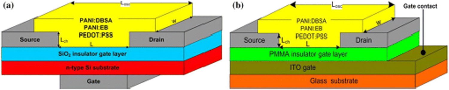 | ||
| Fig. 23 Layout structures of the OFETs as ammonia sensors based on the (a) n-type Si gate with SiO2 insulator layer; (b) ITO gate with the PMMA insulator layer, where Losc = channel length, L = active channel thickness, Lch = channel thickness, and w = channel width (reproduced with permission from ref. 98. Copyright 2019, Springer Nature). | ||
 | ||
| Fig. 24 Molecular structures of (a) PANI/ES and (b) PANI/DBSA and (c) diagram of the sensing mechanism of PANI:DBSA. | ||
| OFET Sensor | Response time (s) | Recovery time (s) |
|---|---|---|
| Si/PANI:DBSA | 2 | 30 |
| Si/PANI:EB | 2 | 27 |
| Si/PEDOT:PSS | 13 | 8 |
| ITO/PANI:DBSA | 4 | 14 |
| ITO/PANI:EB | 33 | 6 |
| ITO/PEDOT:PSS | 29 | 22 |
Lee et al. fabricated the OFET-based sensor using pentacene OSC to detect hydrochloric acid (HCl) gas concentrations.99 OFET displayed the field-effect mobility of 1.8 cm2 V−1 s−1, subthreshold slope of 0.64 V dec−1, threshold voltage of 5.6 V and on/off current ratio of 106. The sensing mechanism for these devices was closely related to the carrier transport and charge transfer. Oxygen molecules were adsorbed on the surface of the pentacene film upon exposure to dry air. Therefore, oxygen species such as O2−, O− and O2− were present on the surface of the film, capturing electrons inside the film. However, saturation occurred after adsorption of enough oxygen, and no further change in the current was observed. Pentacene is a p-type semiconductor with π-combination and the holes are major charge carriers. The weak binding oxygen adsorption on the surface of pentacene was replaced by HCl when exposed to HCl gas. HCl reacted with the oxygen species attached to the surface of the pentacene and generated an extra Cl−, which captured the additional electron present in the pentacene, resulting in an increased IDS. As the concentration of HCl was changed repeatedly, the reactivity increased systematically as the HCl gas increased from 3 to 20 ppm. The maximum response of the pentacene OFET was 1.55 at the HCl concentration of 3 ppm, while the recovery time to its initial state was about 200 s at the concentration of 20 ppm at room temperature. Hence, the fabricated devices did not corrode even with HCl exposure and recovered to their initial state.
Huo et al. synthesized a series of dicyanomethylene-terminated quinoidal compounds (Fig. 25) to be used as the active channel in n-type OFETs for detecting DMMP.100 Mobilities of these OFETs ranged from 10−3–10−1 cm2 V−1 s−1. The current change ratio gradually increased by increasing the DMMP gas concentration; the IDS current change ratios of compounds 4-T-PTZCN, 3-T-PTZCN and 3-T-TZCN reached up to 17%, 9% and 7%, respectively, under the action of 10 ppm DMMP gas. Compound 3 displayed the best detection sensitivity and selectivity. The response value remained at 0.5–1% even when the gas concentration was decreased to 10 ppb. Moreover, the sensor devices were tested with a series of gases as the interfering gas with the concentration of 10 ppm to verify the selectivity of the new sensors based on 3-T-TZCN to DMMP. The sensors based on 3-T-TZCN displayed more obvious response behavior of 17% to DMMP, and the response values of the other interfering gases were no more than 2.6%. Additionally, the impact of the humidity on the sensing performance of compounds 1–3 was evaluated with the 10 ppm DMMP vapor under different humidity conditions by employing lithium chloride to control the humidity level. The sensing response of all three sensors was decreased with the increase of the relative humidity. With the humidity above 60%, the decrease was significantly high. Meanwhile, the decrease was minimal when the humidity was below 60%. The degree of decline of 3-T-TZCN was obviously lower compared to the other two compounds. Furthermore, the sensing response was still effective for the detection of DMMP even under the high humidity condition of 75%. In OFETs based on 3-T-TZCN, the mobility decreased by no more than 18% after 90 days of being stored in air atmosphere.
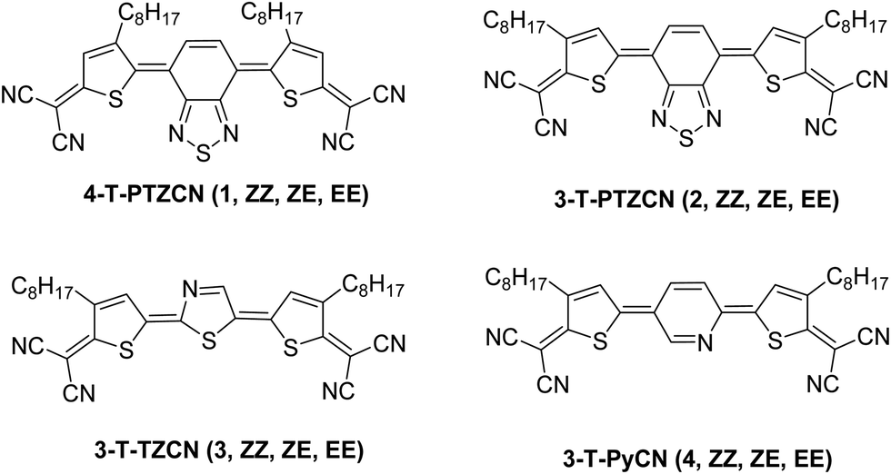 | ||
| Fig. 25 Different heterocycle-based quinoidal compounds. | ||
Data related to the device design and performance of OFET-based gas sensors have been summarized in Table 14.
| OFET's configuration | OSC/active layer | Dielectric layer | Gas to be sensed | Device performance | Ref. |
|---|---|---|---|---|---|
| BGTC | Poly{2,2′-[(2,5-bis(2-octyldodecyl)-3,6-dioxo-2,3,5,6-tetrahydropyrrolo[3,4-c]pyrrole-1,4-diyl)]dithiophene-5,5′-diyl-alt-2,2′-bithiophene-5,5′-diyl} (PDQT) | SiO2 | NH3, H2S, NO2 | • Responsivity = 780% towards NO2 | Song et al.67 |
| • LOD = 1 ppm. | |||||
| BGTC | Copper phthalocyanine (CuPc) deposited on a well-ordered polyvinyl alcohol (PVA) parallel nanofiber arrays (PNAs) | SiO2 | NO2 | • Detection of NO2 at 0.3 ppm concentration. | Wang et al.68 |
| • Response time = 0.02 min | |||||
| • Recovery time = 0.02 min | |||||
| BGTC | Copper phthalocyanine (CuPc) on p-6P template | Al2O3 + PMMA | NO2 | • Sensitivity = >129%/ppm | Xie et al.72 |
| • LOD = <1 ppm (134%) | |||||
| BGTC | Dinaphtho[2,3-b:2′,3′-f]thieno[3,2-b]thiophene (DNTT) | PMMA | NH3 | • Response = <1 min | Darshan et al.82 |
| • Recovery = 90% of the initial state within 2 min | |||||
| • LOD = 100 ppb | |||||
| BGTC | Dinaphtho[2,3-b:2′,3′-f]thieno[3,2-b]thiophene, (DNTT) with solvatochromic Nile red (NR) sensing medium. | Parylene-C | NH3 | • Response and recovery rates were improved by 46 and 94%, respectively. | Oh et al.81 |
| • Sensitivity = 0.87 ± 0.045 ppm−1%. | |||||
| BGTC | Poly[3-(3′′,4′-difluoro-[2,2′:5′,2′′-terthiophen]-5-yl)-2,5-bis-(5-octylpentadecyl)-6-(thiophen-2-yl)pyrrolo[3,4-c]pyrrole-1,4(2H,5H)-dione] (5-PDBF) + poly[3-(3′′,4′-difluoro-[2,2′:5′,2′′-terthiophen]-5-yl)-2,5-bis(2-octyldodecyl)-6-(thiophen-2-yl)-pyrrolo[3,4-c]pyrrole-1,4(2H,5H)-dione] (2-PDBF) + poly[3-(3′′,4′-difluoro-[2,2′:5′,2′′-terthiophen]-5-yl)-2,5-bis(3-(2-(2-methoxyethoxy)ethoxy)-2-((2-(2-methoxyethoxy)-ethoxy)-methyl)-propyl)-6-(thiophen-2-yl)-pyrrolo[3,4-c]pyrrole-1,4(2H,5H)-dione] (2EO-PDBF) | SiO2 | NO2 | • 2EO-PDBF sensor displayed fast and reversible detection with an LOD of 0.24 ppb. | Kang et al.83 |
| • Selectivity towards NH3, SO2 and CO2. | |||||
| BGBC | 1,3-Bis[11-(7-hexyl[1]-benzothieno-[3,2-b][1]benzothien-2-yl)undecyl]-1,1,3,3-tetramethyldisiloxane, O(Si-Und-BTBT-Hex)2 | SiO2 | NH3, H2S | • Multiparametric detection of toxic gases via different sensing mechanisms. | Sizov et al.84 |
| BGBC | Benzothieno[3,2-b][1]-benzothiophene (BTBT) disiloxane derivative (D2-Und-BTBT-Hex) + metalloporphyrins | PMMA | H2S, NO2, Et-SH, NH3 | • LOD = 30–470 ppb range | Anisimov et al.85 |
| • Operates in air with up to 95% relative humidity | |||||
| • Capable to discriminate chemically different gases, such as NO2 and NH3, as well as similar ones as H2S and ethanethiol | |||||
| BGTC | Poly(bisdodecylquaterthiophene) (PQT-12)/polystyrene (PS)blend film | SiO2 | NO2 | • LOD = 200 ppb towards NO2. | Fan et al.87 |
| • Sensitivity = 25 and 400% for NO2 concentrations of 200 ppb and 20 ppm, respectively | |||||
| BGTC | Dithienyl diketopyrrolopyrrole–fluorene-based polymers | SiO2 | NH3 and NO2 | • LOD = 0.5 ppm | Makhopadhyaya et al.88 |
| • The proportional on-current change of OFETs using a dithienyl DPP−fluorene polymer reached ∼614% for an exposure to 20 ppm of NO2 for five minutes. | |||||
| • Increased susceptibility was displayed to oxidizing NO2 compared to reducing gas NH3. | |||||
| BGTC | Dithienyl diketopyrrolopyrrole–fluorene and dithienyl diketopyrrolopyrrole–bithiophene-based polymer | SiO2 | NH3 and NO2 | • Recovery from bias stress, in the ambient atmosphere, was faster for diketopyrrolopyrrole–bithiophene-based polymer (P6) while diketopyrrolopyrrole–fluorene-based polymer (PF2) showed the least tendency to refill the created traps. | Makhopadhyaya et al.89 |
| • Polymers retained their NO2 sensitivity both post NO2-aided recovery and air-aided recovery at a bias stress condition of VG = VD = −80 V. | |||||
| BGTC | PTQ-TEG/PTQ-T | SiO2 modified by octadecyl trichlorosilane (OTS) | NO2 | • Higher NO2 sensitivity with a faster recovery rate was shown by PTQ-TEG | Ahn et al.90 |
| • Order of detection sensitivities: NO2 = 6.9%/ppm, SO2 = 0.03%/ppm, NH3 = 0.05%/ppm, CO2 = 0.19%/ppm, | |||||
| BGTC | Poly(3-hexylthiophene-2,5-diyl) (P3HT) + poly(9-vinylcarbazole) (PVK) | PMMA | NO2 | • LOD = 300 ppb | Yang et al.91 |
| • Current sensitivity = ∼12381% for 15 ppm with 50% P3HT |
|||||
| BGTC | N,N-Diperfluoroheptyl naphthalene diimide (F-NDI) | AlOx + benzocyclobutene derivative (BCB) | NH3, Amines (dimethylamine, trimethylamine) | • LOD = >1 | Sagdullina et al.92 |
| • Response time = ≤10 s | |||||
| BGTC | (E)-1,2-Bis(5-(naphthalen-2-yl)thiophen-yl)ethene (TVT-NA), (E)-1,2-bis(5-(benzo[b]thiophen-yl)thiophen-2-yl)ethene (TVT-BT) and (E)-1,2-bis(5-(benzofuran-2-yl)thiophen-2-yl)ethene (TVT-BF) | SiO2 | NH3 | Response and recovery time = within 20 to 30 s | Huo et al.93 |
| BGTC | Indacenodithiophene-benzothiadiazole (IDTBT) | SiO2 | NH3, NO | • Device selectivity was reversed under two different conditions, i.e., darkness and illumination | Zhao et al.94 |
| • Sensors operating in dark conditions have improved response towards oxidizing NO | |||||
| • Under light conditions, the removal of hole traps via photoexcitation facilitates the regeneration of hole trap by reducing NH3 | |||||
| BGBC | [2,5-(2-Octyldodecyl)-3,6-diketopyrrolopyrrole-alt-5,5-(2,5-di(thien-2-yl)thieno] [3,2-b]thiophene) (DPP-T-TT) | P(VDF-TrFE-CFE) + PMMA | Amine vapors (alkyl-amines, trimethylamine, triethylamine, n-propylamine, n-butylamine and dibutylamine) | • LOD = 0.025 ppb (dibutylamine) | Mougkogiannis et al.95 |
| • Sensitivity = 10.00 ± 0.20% ppb−1 (dibutylamine) | |||||
| BGTC | Pentacene + 6,13-bis(tri-isopropylsilyethynyl) | SiO2 | NH3 | • Response time = 26 s | Lee et al.97 |
| Pentacene (TIPS–pentacene) | • Recovery time = 340 s | ||||
| BGBC | Polyaniline doped with dodecylbenzene sulfonic acid “DBSA” (PANI:DBSA), polyaniline–emeraldine base (PANI:EB), and poly(3,4-ethylenedioxythiophene):polystyrene sulfonate (PEDOT:PSS) | SiO2 or PMMA | NH3 | • Relative response (ΔR) = ∼ 63% and ∼ 41.4% | Amer et al.98 |
| • Response time = 2 and 4 s (for PANI:DBSA) | |||||
| BGTC | Pentacene | SiO2 | HCl | • Maximum response = 1.55 at 3 ppm conc. | Lee et al.99 |
| • Recovery time = 200 s | |||||
| BGTC | Dicyanomethylene-terminated quinoidal compounds, 4-T-PTZCN, 3-T-PTZCN and 3-T-TZCN | SiO2 | DMMP | • 3-T-TZCN displayed more obvious response behavior of 17% to DMMP | Huo et al.100 |
| • Detection of DMMP in high humidity of 75%. | |||||
| • In 3-T-TZCN sensors, the mobility decreased no more than 18% after 90 days stored in air atmosphere. |
2.2. Pressure sensors
OFET-based flexible pressure sensors have attracted increased attention in recent years, owing to their inherent properties, such as high array uniformity, excellent signal amplification, excellent stress monitoring, facile integration with electrical circuitry and high spatial contrast. These sensors are vital components for future practical electronic applications, including electronic skin, rollable displays and for the next generation of wearable health care devices.101–104 A prerequisite for the majority of these applications are as follows: low power consumption, reduced production cost and enhanced flexibility to enable device integration on curved surfaces and eventually on human skin.105 Organic-based electronics present an attractive option considering these requirements, as they are compatible with low-cost fabrication protocols, and can be deposited at low temperature and on plastic substrates. For the aforementioned applications, pressure sensitivity in a low-pressure regime, i.e., <10 kPa is crucial. So far, three transduction mechanisms have been reported for converting pressure stimuli into electrical signals, which are capacitance changes,103,106 piezoelectricity107,108 and piezoresistivity.109,110 OFETs have successfully been employed as electrical transduction platforms in pressure sensors. OFETs can be used in devices for transmitting information from pressure-responsive components, or alternatively, their electrical response to pressure can also be exploited. Until now, researchers have obtained encouraging results, but most of these devices need a high operation voltage. Recently, polyelectrolyte-gated OFETs have emerged as promising low-voltage devices for advanced sensing. However, the real applications of these sensors are greatly limited by their poor stability, severe hysteresis and low sensitivity. Polar polyelectrolytes are hygroscopic. Hence, they easily absorb moisture, which adversely effects the OSC. Meanwhile, polyelectrolyte-induced dipolar disorder, leakage currents and parasitic capacitance can cause severe hysteresis and poor interfacial compatibility, which are damaging for the electrical performance and operational stability of OFETs.111,112 The improvement in hysteresis induced by residual dipoles or mobile ions still remains an obstacle toward affording sensors with low operating voltages and relatively high sensitivity.113–116Liu et al. reported on hysteresis-free polyelectrolyte-gated OFETs for ultrasensitive low-power pressure sensors achieved via nanoscale dielectric interface passivation.117 The hysteresis and leakage currents of the polyelectrolyte-gated OFETs were largely suppressed by incorporating a thin polymer passivation layer between the binary polyelectrolyte dielectric and OSC layers. Hysteresis-free OFETs with this composite dielectric of polystyrene/polyelectrolyte were developed into flexible low-power pressure sensors, which delivered an exceptionally high sensitivity of 897.9 kPa−1 at a low-operating voltage of −2 V. Fig. 26b shows the changes in the operating mechanism of these devices without and with interface passivation by the thin nanoscale polystyrene layer. In the polyelectrolyte composite film, PEG serves as a non-ionic component and PAA dielectric is a polyanionic proton conductor. With both PAA and PEG as hydrophilic in nature, they easily absorbed moisture in air conditions. In particular, the hygroscopic PEG rapidly absorbed water, and effectively promoted the anion migration and ion conduction due to the decreased activation energy. The cations and anions mainly originate from the dissociation of PAA, which produced the H+ cations and deprotonated polyanions. Since these devices were operated in an ambient environment (60% RH), hydroxide (OH−) anions were naturally generated from the dissociation of water. Therefore, for the bare PAA:PEG-based OFETs under the negative gate potential (the left of Fig. 26b), the free H+ cations moved to the side of the gate electrode interface. The deprotonated polyanions could then gather close to the semiconductor surface, but did not migrate into the un-passivated PIDT-BT:TCNQ film due to the diffusional restrictions of the polymer backbone. Meanwhile, the mobile OH− were able to penetrate deeply into the un-passivated OSC layer, causing the charge carriers to exist both on the channel surface and in the bulk structure of the doped OSC. Consequently, the electrostatic charging mechanism of the field-effect induced mode was critical to these polyelectrolyte-gated OFETs. One of the drawbacks determined by this operating mechanism was that the ions took more time to migrate across the layers, leading to the relatively large hysteresis and slow response time of OFETs. This issue was addressed by employing a hydrophobic PS as a thin interface passivation layer to improve the interfacial compatibility and restrict ion migration into the active layer, avoiding the doping of bulk semiconductors.
 | ||
| Fig. 26 (a) Schematic architecture of the flexible OFETs and molecular structures of PS, PAA, PEG, PIDT-BT and TCNQ. (b) Mechanism of the OFETs in electrochemical doping (left) and electrostatic charging (right) modes (reproduced with permission from ref. 117. Copyright 2022, Elsevier). | ||
Sun et al. developed a high-k Al2O3 dielectric on aluminum foil via simple printing protocol for OFETs and pressure sensor.118 The high-k Al2O3 dielectric films were large-area compatible and robust, leading to a high areal capacitance and low leakage current density. These OFET devices exhibited a field-effect mobility of 0.65 cm2 V−1 s−1 and current on/off ratio of up to 105. Additionally, these OFET devices displayed good mechanical stability and excellent uniformity, indicating the printed Al2O3 dielectric as a promising candidate for the fabrication of OFETs on a large scale. The extended gate OFET-based pressure sensor achieved a high-pressure sensitivity of 8 kPa−1 at an operational voltage of as low as −2 V and a fast response time of <100 ms (Fig. 27).
 | ||
| Fig. 27 (a) 3D illustration of the extended gate OFET-based pressure sensor without pressure (left) and with pressure (right). (b) Side view of the illustration of the device without pressure (left) and with pressure (right) (reproduced with permission from ref. 118. Copyright 2019, ACS). | ||
Wang et al. reported a sensor based on the semiconductor/conductor interface piezoresistive effect in OFETs, which merged the merits of field-effect modulation and piezoresistive effect.119 The piezoresistive effect was activated by the gate modulation. The schematic fabrication process of the piezoresistive sensor is shown in Fig. 28a. Polydimethylsiloxane (PDMS) with micropyramids and Au were deposited as a couple electrodes. PDMS/Au were laminated onto the DNTT OSC layer as drain/source electrodes to form the OFET-based sensors. The working principle of these sensors was mainly based on the tunable contact quality between OSC and drain/source electrodes, as well as the gate modulation. When pressure was applied on the PDMS electrode, the pyramidical peaks were deformed. The increased contact area between OSC and the electrode improved the carrier's injection efficiency, and hence decreased the contact resistance. The effective channel length was decreased when the PDMS/Au micropyramids were deformed to a larger contact area under pressure (Fig. 28b). This contributed to the reduction of the channel resistance, but the change range of the channel length was limited while the actual channel width showed no change or only a small change during the deformation of the microstructured electrode. Therefore, the deformation of micropyramids altered the electrode/OSC contact resistance, and simultaneously tuned the channel resistance in a relatively small range. Moreover, the conductivity of the channel was closely related to the amount of charges induced by the gate voltage. Thus, this conductor/semiconductor piezoresistive effect also took advantage of the electric-field modulation effect. These sensors exhibited a sensitivity of up to 514 kPa−1 after applying an appropriate voltage. The response time was found to be 1.8 ms during loading and 6.7 ms during unloading, with a high durability of over 10000 cycles. The LOD value was as low as 10 Pa, which was located in the subtle-pressure regime (1–1000 Pa). These device sensors successfully sensed the motion of the wrist, and accurately captured the weak signals of the wrist pulses.
 | ||
| Fig. 28 (a) Schematic fabrication process of the pressure sensor. (b) Schematic diagrams of the change of the channel length (reproduced with permission from ref. 119. Copyright 2019, WILEY). | ||
Liu et al. constructed a multifunctional flexible OFET by inserting a charge-transfer complex with piezo-sensitive microstructures modified on the OSC layer (DPP-DTT) through one-step spin-coating.120 The charge-transfer complex consisted of 7H-dibenzo[c,g]carbazole/7,7,8,8-tetracyanoquinodimethane (DBCz/TCNQ) polymer solutions. Poly[[2,3,5,6-tetrahydro-2,5-bis(2-octyldodecyl)-3,6-dioxopyrrolo[3,4-c]pyrrole-1,4-diyl]-2,5-thiophenediylthieno[3,2-b]thiophene-2,5-diyl-2,5-thiophenediyl] (DPP-DTT) was used as an OSC layer. The organic charge-transfer complex is a new class of OSCs, containing two or more types of components in a highly-ordered molecular-level-heterojunction packing state. The buffer layer structure was well controlled by doping proportion tuning, undergoing a clear phase separation. The possible sensing mechanism of these devices is shown in Fig. 29e. The nanoribbon-shaped donor–acceptor complex remained in its initial state in the absence of external pressure and the devices operated in their original state. The DBCz/TCNQ framework underwent compression with spontaneous displacement and polarization under the influence of an external pressure. Current flow and the electrical potential were generated, leading to a gradual change in capacitance. Perhaps, there was friction electrification from the PMMA layer and microstructure. In this case, the polarization of the DBCz/TCNQ co-crystal microstructures altered the relative capacitance of the dielectric upon pressures and the output current, due to their non-centrosymmetric lattice structure and the mismatch between the insulator and co-crystal. Consequently, the as-prepared sensors presented significant pressure-stimuli responses and even thermo-sensitive behaviors. For pressure sensing, a good sensitivity of 2.73 kPa−1 was achieved with a very low-pressure detection limit and a fast response time of ≈0.13 s.
 | ||
| Fig. 29 (a) Structure of the prepared sensing device, (b) piezo-sensitive mechanism of the DBCz/TCNQ-doped device (reproduced with permission from ref. 120. Copyright 2023, WILEY) and (c) molecular structures of DBCz and TCNQ. | ||
Yin et al. developed bilayer polymer dielectrics for low-voltage OFET-based pressure sensors.121 A novel type of bilayer dielectrics was generated with the help of facile solution processing by combining the thin PMMA with controlled thicknesses with a thick polyelectrolyte of polyacrylic acid (PAA) (Fig. 30). This multifunctional dielectric layer provided a vertical phase separation structure with good stability, significant depletion in leakage currents and high capacitance. Consequently, the flexible OFETs with the PMMA/PAA dielectrics maintained low-voltage operation and displayed better electrical performance than the devices consisting of a pure PAA dielectric. Moreover, a suspended gate was used for the OFET-based sensor, and an optimized PMMA/PAA dielectric layer was employed to achieve highly sensitive pressure sensing. The pressure sensors displayed a record high sensitivity of 56.15 kPa−1 at a low operating voltage of −5 V, a fast response time of less than 20 milliseconds, bending stability with over 2000 cycles under a bending radius of 3 mm and adequate flexibility. This study demonstrated a convenient protocol for the construction of low voltage, highly sensitive pressure sensors for practical e-skin applications.
 | ||
| Fig. 30 (a) Structure of the flexible OFET device. (b) Molecular structures of PIDT-BT, TCNQ, PAA, and PMMA (inset is an illustration of the PMMA/PAA dielectric with a vertical phase separation structure) (reproduced with permission from ref. 121. Copyright 2018, WILEY). | ||
Zhang et al. reported on a hydrogel-based electrolyte-gated OFET (HYGOFET), where a soft water-based agarose hydrogel layer was used as a dielectric layer.122 Water is known to orientate under the influence of an electric field due to its dipolar nature, and such orientation can be affected by the application of pressure. The hydrogel layer provided a high-capacitance dielectric, maintained a constant saturated humid environment to the active OSC layer and reduced the operational voltage. The chemical structures of OSC, 2,8-difluoro-5,11-bis(triethylsilylethynyl)anthradithiophene (diF-TES-ADT) and agarose hydrogel are shown in Fig. 31. The HYGOFET displayed high electrical performance and long-term stability due to a polydimethylsiloxane (PDMS) encapsulation structure. When pressure was applied, a negative Vth shift and consequent IDS decrease were observed, followed by a full recovery of the initial transfer characteristics when the pressure was removed. Upon application of pressure, the orientation of the entrapped water molecules in the OSC was changed, which affected the local polarization of the OSCs; hence, creating states in the band gap, and Vth was shifted due to these traps. The electrical characteristics of these sensors responded to the application of low pressures, i.e., in the range of several hundred Pa to 9 kPa. These devices operated in a voltage window below 0.5 V and their shelf-stability was estimated to be around 2 days. The time response of the HYGOFET toward pressure was estimated to be ≈2 s.
 | ||
| Fig. 31 Chemical structures of OSC, 2,8-difluoro-5,11-bis(triethylsilylethynyl)anthradithiophene (diF-TES-ADT) and the agarose hydrogel dielectric. | ||
Lai et al. investigated the electromechanical performance of OFET-based sensors to better understand the role of the source-drain electrodes layout, along with the morphology of OSC obtained by different patterning methods.123 Two different sensor structures, with interdigitated and spiral-shaped source and drain electrodes, were employed along with the solution-processed OSC. OSC was deposited by drop-casting or patterned by using meniscus-guided printing (Fig. 32). This approach allowed the orientation of the crystalline domains to specific directions, and provided isotropic or anisotropic semiconductor patterns onto the transistor's channel area. An anisotropic surface strain was imposed for testing different device configurations as strain gauges and tactile sensors. Sensors with spiral-shaped electrodes in combination with isotropic semiconductor patterning were found to be more useful for reproducing the sense of touch, while interdigitated devices with crystalline domains aligned along the channel length direction came out to be ideal strain gauges. These investigations could pave the way to the development of e-skin for prosthetic and bio-robotic applications, and for monitoring joint motion and tactile sensing.
 | ||
| Fig. 32 (a) The s-OFET and i-OFET layouts, (b) different organic semiconductor patterns and deposition techniques used, (c) kinds of mechanical deformations employed during device testing as sensors (reproduced with permission from ref. 112. Copyright 2024, Elsevier). | ||
Lai et al. reported on an OFET-based strain sensor in the form of a wearable platform for monitoring the wrist flexion and extension.124 A novel device that was capable of operating below ≤2 V was fabricated over flexible plastic substrates. These devices could be integrated in a custom-made Lycra® glove for monitoring wrist motion without affecting the natural movements, and interfaced with a portable readout electronic module. Initially, devices were embedded in a fabric strip. Afterwards, they were inserted into a pocket sewn in the glove of the corresponding wrist. The current variation in the transistor structure was transduced by the readout electronics into a voltage signal, opportunely conditioned and converted for proper acquisition by the elaboration unit. Users could set different control signals, including sensor polarization and overall amplification, calibrate sensor, and finally record and visualize the real-time signal with the help of a control software. Two kinds of wrist movements, namely flexion and extension, were considered. The sensing response was dependent on the strain induced by the mechanical deformation related to wrist movements. A sensitivity of 14 nA deg−1 and 18 nA deg−1 was obtained for the wrist extension and flexion, respectively. This sensing platform was able to discriminate bending angles as low as 6° for both kinds of wrist movements with significant reliability.
Wang et al. used the fully flexible piezoelectric tactile sensor based on the piezotronic effect by integrating piezoelectric materials with the mechanical-to-electrical conversion function of β polyvinylidene fluoride (PVDF) nanorod arrays and the signal amplification function of OFETs.125 The tactile sensor array consisted of a 3 × 3 cell on a polyethylene terephthalate (PET) substrate for effectively measuring the wrist curvature at different degrees (Fig. 33). An external mechanical force was transformed into piezoelectric voltage for driving the OFETs by employing the PVDF nanorod arrays, which considerably improved the piezoelectric properties of the materials. Piezotronic transistors converted pressure into electrical signals without applying a gate voltage, which substantially simplified the circuit models and sensor distribution. The sensitivity of the tactile sensor could be improved by amplifying the piezoelectric voltage using an OFET. The fabricated tactile sensor displayed a pressure sensitivity of 5.17 kPa−1, detection limit of 175 Pa and response time of 150 ms.
 | ||
| Fig. 33 Fully flexible piezoelectric tactile sensor based on the piezoelectronic effect (reproduced with permission from ref. 125. Copyright 2020, Elsevier). | ||
Thuau et al. investigated the effect of the layer thickness of OSC (ranging from 5–15 nm) on the piezoresistive sensitivity of the dinaphtho[2,3-b:2,3-f]thieno[3,2-b] thiophene (DNTT) OSC layer.126 The device architecture was a CantiFET, an OFET embedded in a suspended organic micro-cantilever (Fig. 34). The triangular shape of the cantilever was chosen to induce uniform longitudinal stress in the DNTT thin film when a force was applied at the free end of the cantilever. The DNTT layer with the thickness ranging from 5 nm to 30 nm was investigated. No significant changes in the transfer curves were observed above 15 nm thickness. A 5 nm thick active layer was not adequate to turn on the OFET due to the unavailability of the charge carrier transport. IDS was found to decrease with the decrease in the DNTT thickness from 15 to 6 nm due to the hindered charge carrier transport along the transistor channel. The on-state IDS values of OFETs with DNTT thicker than 15 nm did not vary as the charge carrier transport takes place in the first few nanometers next to the dielectric interface, provided that complete coverage is attained. 6 nm was the minimum thickness that allowed charge transport in the DNTT layer, which was the critical thickness, where the percolation path was achieved between the DNTT grains. Moreover, a decrease in the active layer thickness also increased the morphological defects. Hence, as a result, the charge trapping sites slightly shifted the Vth from −1.6 V for a 15 nm thick active layer towards higher VGS at −2.2 V for 8 and 6 nm thick film. Gauge factors (GFs) of 42 ± 5 and −31 ± 6 were measured from the variation of the output currents of the 6-nm thick DNTT-based OFETs engineered on top of the polymer cantilevers in response to the compressive and tensile strain, respectively. Generally, the GF is defined as the normalized change of the resistance per applied strain, GF = (ΔR/R0)/ε, where ΔR is the change in the resistance as compared to the unstrained device, R0 is the resistance of the unstrained device, and ε is the applied strain.
 | ||
| Fig. 34 Schematic side view of the CantiFET device and its corresponding cross-section (reproduced with permission from ref. 126. Copyright 2020, MDPI). | ||
Yin et al. reported on a fully flexible, breathable, water-proof piezoelectric sensor by capacitive coupling of the polyvinylidene fluoride (β-PVDF) nanofiber membrane (NM) with the electromechanical conversion function OFET device with signal amplification function.127 The inherent waterproofed β-phase PVDF NM with thousands of micropores was fabricated by advanced electrospinning process, which provided the device with excellent breathability. PVDF NM also improved the deformation tolerance and accelerated the response/recovery time. Hence, the device could be bent at will without affecting its performance. Based on the piezoelectric effect polarization, the charge generated by the PVDF membrane was sufficient to drive the OFET device and monitor human physiological signals without applying a gate voltage. Based on the concept of the piezoelectric effect that the piezoelectric potential energy could regulate and control the current in OSC, PVDF NM as signal input unit was connected with OFET as a piezoelectric signal output unit. Therefore, the PVDF-OFET-PZTS was constructed, as shown in Fig. 35. The PVDF piezoelectric NM produced a positive voltage upon deformation that operated as the gate voltage in the OFET when mechanical force was applied. The holes produced from diphenylamine (DPA) accumulated at the interface between the gate, and the dielectric layer induced additional electrons in the DPA channel. Furthermore, the recombination of the electrons with the holes occurred in the channel, resulting in a decreased current. The PVDF recovered and deformed to generate a negative voltage upon the release of mechanical force, and electrons were accumulated at the interface between the dielectric and gate, inducing additional holes in the DPA channel, resulting in increased current due to the increase in holes. This principle allowed the mechanical signal to be converted to electrical signal without adding an extra gate voltage. The signal detected by PVDF-OFET-PZTS was nearly 1000 times larger than that generated by the PVDF piezoelectric NM under the same external force. This result proved the excellent signal amplification function of DPA-OFET. These tactile sensors displayed a pressure sensitivity of 7.94 kPa−1, detection limit of 48.54 Pa and response time of 105 ms.
 | ||
| Fig. 35 Composition diagram of PVDF-OFET-PZTS. The PVDF NM was coupled in parallel with DPA-OFET (reproduced with permission from ref. 127. Copyright 2023, Elsevier). | ||
Data related to the device design and performance of the OFET-based pressure sensors have been summarized in Table 15.
| OFET's configuration | OSC/active layer | Dielectric layer | Additional layer/segment | Mobility and sensing response | Ref. |
|---|---|---|---|---|---|
| GF = normalized change of resistance per applied strain, GF = (ΔR/R0)/ε. | |||||
| TGBC | Poly(indacenodithiophene-co-benzothiadiazole) (PIDT-BT) + tetracyanoquinodimethane (TCNQ) | polyacrylic acid:poly(ethylene glycol) (PAA:PEG) | Polystyrene (PS) passivation layer | • Mobility = 0.14 to 2.89 cm2 V−1 s−1 | Liu et al.117 |
| • Sensitivity = 897.9 kPa−1 | |||||
| BGTC | Pentacene | Al2O3 | — | • Mobility = 0.65 cm2 V− 1 s− 1 | Sun et al.118 |
| • Sensitivity = 8 kPa−1 | |||||
| • Response time = <100 ms | |||||
| BGTC | Dinaphtho[2,3-b:2,3-f]thieno[3,2-b]thiophene (DNTT) | SiO2 | • Cytop buffer layer | • LOD = 10 Pa | Wang et al.119 |
| • PDMS with micropyramids | • Sensitivity = 514 kPa−1 | ||||
| • Response time = 1.8 ms during loading and 6.7 ms during unloading | |||||
| • High durability of over 10000 cycles |
|||||
| TGBC | Poly[[2,3,5,6-tetrahydro-2,5-bis(2-octyldodecyl)-3,6-dioxopyrrolo[3,4-c]pyrrole-1,4-diyl]-2,5-thiophenediylthieno[3,2-b]thiophene-2,5-diyl-2,5-thiophenediyl] (DPP-DTT) | PMMA | 7H-Dibenzo[c,g]carbazole/7,7,8,8-tetracyanoquinodimethane (DBCz/TCNQ) | • Mobility = 1.5 cm2 V−1 s−1 | Liu et al.120 |
| • Sensitivity = 2.73 kPa−1 | |||||
| • Response time = ≈ 0.13 s. | |||||
| TGBC | Poly(indacenodithiophene-co-benzothiadiazole) (PIDT-BT) + tetracyanoquinodimethane (TCNQ) | PMMA + PAA | — | • Sensitivity = 56.15 kPa−1 | Yin et al.121 |
| • Response time = <20 ms | |||||
| • Bending stability = >2000 cycles under a bending radius of 3 mm. | |||||
| TGBC | 2,8-Difluoro-5,11-bis(triethylsilylethynyl)anthradithiophene (diF-TES-ADT) + polystyrene | Agarose hydrogel | PDMS-based encapsulation | • Mobility = 0.8 cm2 V−1 s−1 | Zhang et al.122 |
| • Shelf-stability = 2 days | |||||
| • Response time = ≈2 s | |||||
| BGBC | 6,13-Bis(triisopropylsilylethynyl)pentacene (TIPS) pentacene | Al2O3 + Parylene-C | — | • Sensors with spiral-shaped electrodes in combination with isotropic OSC patterning were more useful for reproducing sense of touch | Lai et al.123 |
| • Interdigitated devices with crystalline domains aligned along the channel length direction were ideal strain gauges | |||||
| BGBC | (6,13-Bis(triisopropylsilylethynyl)pentacene (TIPS) pentacene) | Al2O3 + Parylene-C | Lycra® glove for wrist motion monitoring | • Sensitivity = 14 nA deg−1 and 18 nA deg−1 (for wrist extension and flexion) | Li et al.124 |
| • Able to discriminate bending angles as low as 6° for both kinds of wrist movements | |||||
| BGTC | Pentacene | PMMA | β polyvinylidene fluoride (PVDF) nanorod arrays | • Sensitivity = 5.17 kPa−1 | Wang et al.125 |
| • LOD = 175 Pa | |||||
| • Response time = 150 ms | |||||
| BGTC | Dinaphtho[2,3-b:2,3-f] thieno [3,2-b] thiophene (DNTT) | Al2O3 | Polystyrene as a passivation layer | • GF = > 40 (6 nm thick active layer) | Thuau et al.126 |
| • GF = 12 (15 nm thick active layer) | |||||
| BGTC | 2,6-Diphenylanthracene (DPA) | SiO2 | Polyvinylidene fluoride (PVDF) nanofiber membrane | • LOD = 48.54 Pa | Yin et al.127 |
| • Pressure sensitivity = 7.94 kPa−1 | |||||
| • Response time = 105 ms | |||||
2.3. pH sensors
The quality of water/aqueous solutions can be identified by its pH level, which is the measure of the number of hydronium ions.128 The difference in the concentration of hydronium and hydroxyl ions in the water/aqueous solution is responsible for changing its pH level into that of an acid or base. Living cells and organisms in the human body contain water/aqueous solutions. Therefore, the pH level is a critical parameter in human health. On the other hand, changes of the pH value in external environments such as water reservoirs may result in metal corrosion that poses risks to human health.129,130 Drastic changes in the pH of the soil can cause ecological imbalances, causing adverse effects on the biota, fungi, and bacteria, and earthworms, as well as other animals. Also, pH imbalances in marine organisms create disturbances in their acid–base (metabolic) physiology, resulting in changes to the biodiversity, trophic interactions and other ecosystem processes.131 The untreated waste water from industries contains strong acids or alkalis, which threaten waterborne animals.129,132 Therefore, the changes in the pH levels not only impair human health, but also adversely affect the environment.Majeed et al. proposed a pH sensor based on the dual-gate OFET (DG-OFET) for detecting the variations in the aqueous (electrolyte) medium.133 This DG-OFET consisted of pentacene as a semiconducting layer and a source-sided underlapped region, which was sensitive to the aqueous electrolyte environment. The design of a novel OTFT structure using the organic material, pentacene, was proposed for sensing the pH of the electrolyte (Fig. 36). Double gates had been used in DG-OFET for improved sensitivity and performance over a conventional OTFT-based sensor. The change in the ON-current (Ion) was observed due to parallel examination of the electrolytes in two gates underlapping the region of the structure. The change in the drain current was exploited for different pH values and the corresponding charge densities, utilizing the 2D physics-based numerical simulation for the evaluation of the sensitivity of DG-OFET. The simulation results were extracted with the help of the software package Silvaco TCAD-ATLAS. The proposed device displayed a sensitivity of 217.53 mV per pH with SiO2 as the gate oxide. Using high-k dielectric significantly increased the device sensitivity and helped achieve less degradation over time. The maximum sensitivity achieved in this work using Ta2O5 as a dielectric was 555.284 mV per pH, which was more than nine times the Nernstian limit.
 | ||
| Fig. 36 Schematic of our proposed dual-gate pentacene-based OFET pH sensor with the dual underlap lap region (reproduced with permission from ref. 133. Copyright 2023, MDPI). | ||
Pfattner et al. reported on reversible and stable pH sensors employing a solution processable semiconductor poly(tetrathienoacenediketopyrrolopyrrole) (PTDPPTFT4).134 This device consisted of a BGBC configuration with a pH active top dielectric in a dual-gate device configuration for rapid and continuous measurements in physiologically relevant salt concentrations and pH values (Fig. 37). A silicon wafer was employed as a substrate with thermally grown SiO2 as the bottom dielectric. Meanwhile, for the top dielectric, thermally evaporated SiOx was used due to the presence of many hydroxyl groups on its surface and the mild conditions of thermal evaporation. A key novelty of this approach on the one hand was the good encapsulation of the OSC by a top dielectric, which enabled the device to function in the field-effect regime rather than the electrochemical doping regime. On the other hand, no external voltage was applied to the electrolyte solution; instead, a reference/ground electrode was electrically connected to the source electrode and kept the electrolyte solution potential from drifting. Hence, an externally induced electrical bias across the active sensing layer was significantly reduced, subsequently enhancing the device stability and sensitivity. This double-gate FET platform displayed stable, fast and reversible responses to pH with a sensitivity of up to 39% per pH and resolution of ΔpHFET = ±0.02.
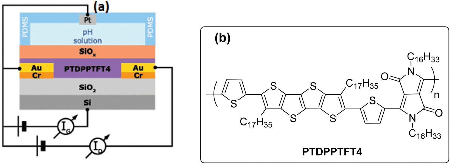 | ||
| Fig. 37 (a) A pH sensor based on the BGBC dual-gate OFET and SiOx as the active sensing layer (reproduced with permission from ref. 134. Copyright 2019, WILEY), (b) chemical structure of PTDPPTFT4 used as a semiconductor. | ||
In this double-gate OFET, the PDMS flow cell was incorporated with a Pt ground electrode. The Pt electrode was used to ground the electrolyte solution without applying an external voltage bias, allowing the sensing voltage to be solely determined by the potential change at the SiOx/electrolyte interface. This approach decoupled the control voltage from the sensing voltage. The OFET was operated in its linear regime with constant drain and gate biases, and its response to different pH values (2.8, 7.4, 11.2) was investigated. The device displayed fast and reversible responses with minimal changes in the gate-leakage current. The sensor's response was quantified and showed a linear relationship with pH values from 5 to 11, with high sensitivity (39 ± 2% per pH) and excellent linearity (0.996). The resolution was found to be ΔpH = ±0.02. Below pH 5, however, the sensor's response deviated from linearity and became independent of pH, possibly due to the high H3O+ concentrations causing a positive surface charge and switching off the transistor. This behavior was consistent with changes in transconductance observed at various gate voltages. The working point of the double-gate structure was chosen at VD = −0.5 V and VG = −5 V, where the sensor was able to respond linearly to pH values higher than 5. This is in good agreement with physiologically relevant conditions. This finding allowed for tuning the linear working range of the OFET. The sensitivity was higher when the working point was close to the threshold voltage of the device. The gate–voltage dependence of the sensitivity was investigated by OFETs driven at different gate voltages. This test showed decreasing sensitivity with increasing gate voltage, as well as decreasing sensitivity with gate dielectric thickness.
Data related to the device design and performance of OFET-based pH sensors have been summarized in Table 16.
| OFET's configuration | OSC/active layer | Dielectric layer | Additional layer/segment | Device performance | Ref. |
|---|---|---|---|---|---|
| TGTC | Pentacene | SiO2 or Ta2O5 | — | • Sensitivity = 217.53 mV per pH (SiO2 dielectric) | Majeed et al.133 |
| • Sensitivity = 555.284 mV per pH (Ta2O5 dielectric) | |||||
| BGBC | Poly(tetrathienoacene-diketopyrrolopyrrole) (PTDPPTFT4) | • SiO2 (bottom dielectric) | PDMS | • Sensitivity = 39% per pH | Pfattner et al.134 |
| • SiOx (top dielectric) | • Resolution, ΔpHFET = ±0.02 |
2.4. Chemosensors
Chemosensing is one of the promising applications of supramolecular analytical chemistry. OFET-based chemosensors have displayed excellent detection abilities for volatile organic chemicals, narcotics and toxic substances,135–137 and have shown advances in their real-time response and high selectivity. Therefore, OFET sensors are expected to be applied in various fields, including environmental detection, food safety, biomedicine and pesticide residues,138,139 especially in areas where flexibility, miniaturization and portability140 are important. Utilizing OFET-based chemosensors for the detection of certain compounds has proved useful in substituting tedious protocols, such as enzyme-coupled colorimetric method141 and ion-exchange liquid chromatography (IELC),142 which are large-scale instrumental strategies that require technical personnel to operate, complicated sample preparation procedures and large equipment. Similarly, oxyanions have been commonly estimated by employing methods requiring large instrumentation, such as gas chromatography-mass spectrometry,143,144 liquid chromatography-tandem mass spectrometry,145,146 and ion chromatography.147 However, the miniaturization of those protocols is very hard to achieve for on-site analysis. Thus, molecular-sized chemosensors for oxyanions have been designed with the possibility of naked-eye detectability of target molecules.148,149 Fabricating a solid-state sensing platform is a useful strategy for the on-site sensing of oxyanions. The self-assembled monolayer (SAM) as the solid-state detection segment can provide multivalent recognition sites, enabling chemical sensing at the interface between the aqueous solution and SAM.150 Consequently, a combination of SAM and a suitable transducer can operate as a portable chemical sensor for target oxyanions. An extended-gate-type OFET, fabricated using SAM, was reported to sense chemical species in aqueous media.151,152 An ingrained cross-reactive response derived from the artificial receptor-based SAM allowed for pattern recognition-driven chemical sensing, leading to the quantitative and qualitative detection of considerable chemical species.153Asano et al. developed a real-time monitoring system utilizing the combination of a water-gated OFET (WG-OFET) and a microfluidic chamber for detecting the potential carcinogenic herbicide glyphosate [N-(phosphonomethyl)glycine] (GlyP).154 The surface of a polymer semiconductor was utilized as a sensing unit for the realization of the real-time sensing with the WG-OFET (Fig. 38). An aqueous solution was used as a gate dielectric that flowed into a designed microfluidic chamber on the semiconductor layer and the gate electrode. This aqueous solution also contained the target analyte. The WG-OFET-based sensor utilized the competitive complexation among the carboxyl side chain of poly[3-(6-carboxylpentyl)thiophene-2,5-diyl] (P3CPT), a copper(II) (Cu2+) ion, and GlyP. P3CPT was used as the polymer OSC, the carboxylate side chain of which could form complexes with Cu2+ at the interface. GlyP strongly coordinated with the Cu2+ ion. Removal of the Cu2+ ion from the Cu2+-P3CPT complex caused selective changes in the electrical double-layer capacitance (EDLC). A uniform water flow and real-time quantitative sensing of GlyP at a micromolar level was enabled by the optimization of the microfluidic chamber.
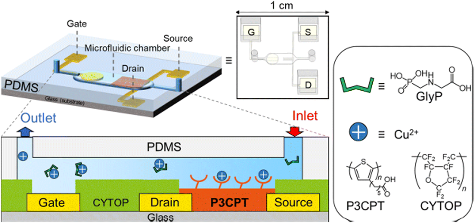 | ||
| Fig. 38 Schematic of the integrated sensing system of WG-OFET and the microfluidic chamber (reproduced with permission from ref. 154. Copyright 2021, ACS). | ||
Fan et al. reported a chemical sensor using an extended-gate-type OFET (EG-OFET) for detecting cocoyl sarcosine (CS) (Fig. 39). The self-assembled monolayer of a dipicolylamine copper(II) complex (Cu2+-dpa) was employed to modify the extended-gate electrode of the EG-OFET, which could capture CS through a coordination bond.155 EG-OFET was utilized for detecting CS in the MES (100 mM) buffer with NaCl (10 mM) at pH 7.0 at 25 °C. An increased CS concentration in the presence of interferents resulted in the shift of the transfer characteristics of the EG-OFET. A positive shift in the transfer characteristics was observed by increasing the concentration of CS (0–10 ppm) at VDS = −2 V. Considering the pH effect, the responses of the fabricated sensor to CS were investigated at three different pH conditions, i.e., 5.5, 6.2, and 7.0. Since deprotonation of the carboxy group of CS would promote the complexation between CS and Cu2+-dpa, the sensor exhibited the highest response to CS at pH 7.0. The LOD was estimated to be 0.03 ppm. The cycle test revealed good reproducibility and reusability of the EG-OFET sensor. Thus, EG-OFET displays great potential for use in maintaining heat equipment in the near future, owing to the industrial applications of CS in heat exchangers.
 | ||
| Fig. 39 Schematic of the EG-OFET structure for CS detection. The extended-gate electrode portion was modified with the Cu2+-dpa complex (reproduced with permission from ref. 155. Copyright 2022, Springer Nature). | ||
Mitobe et al. reported on an OFET-based chemical sensor for multi-oxyanion detection with pattern recognition techniques.156 The oxyanions are known to play versatile roles in biological systems, and accessing the chemical information they provide would be beneficial for fundamental research in diagnosis and pharmacology. Phosphates in human blood serum would be a promising indicator for the early detection of significant diseases. In this regard, phosphate anions that are known as mediators and/or metabolites in cellular signal transduction pathways could be potential markers for indicating abnormal states leading to diseases. In this study, an extended-gate-type OFET was functionalized with a metal complex consisting of 2,2′-dipicolylamine and a copper(II) ion (CuII-dpa), allowing for a compact chemical sensor for detecting oxyanion (Fig. 40). The OFET combined with a uniform CuII-dpa-based self-assembled monolayer (SAM) on the extended-gate gold electrode exhibited a cross-reactive response, suggesting a discriminatory power for pattern recognition. The qualitative detection of 13 oxyanions was demonstrated by only using a single OFET-based sensor with linear discriminant analysis, displaying 100% correct classification (Table 17). The OFET was further applied for the quantification of hydrogen monophosphate in human blood serum using a support vector machine (SVM). The multiple predictions of hydrogen monophosphate at 49 and 89 μM were successfully realized with low errors, which indicated that the OFET-based sensor with pattern recognition techniques would be a practical sensing platform for medical assays.
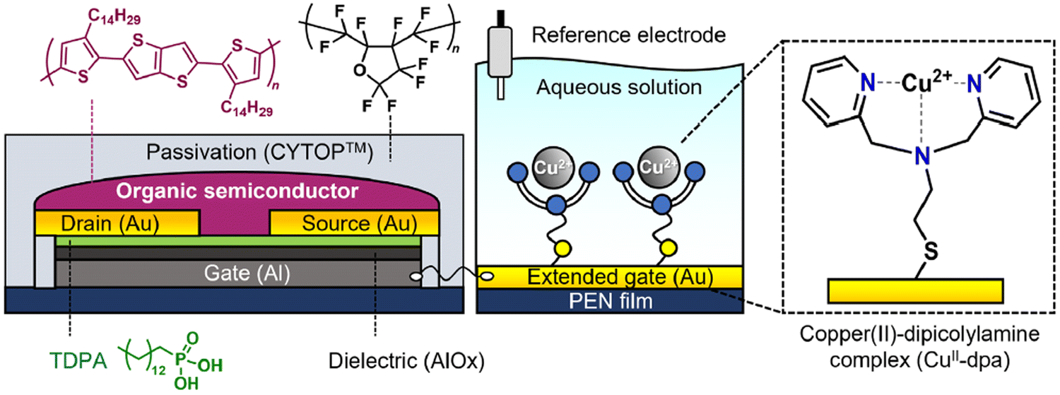 | ||
| Fig. 40 Schematic of the extended-gate-type OFET for oxyanion detection. The extended-gate electrode was functionalized with the CuII-dpa complex (reproduced with permission from ref. 156. Copyright 2022, ACS). | ||
| Oxyanion | Chemical structure | Oxyanion | Chemical structure |
|---|---|---|---|
| Malonate |
|
Phosphate |

|
| Benzoate |

|
Pyrophosphate |
|
| AMP |
|
Acetate |
|
| ADP |

|
Terephthalate |
|
| ATP |

|
Lactate |

|
| Phthalate |
|
Oxalate |

|
| Isophthalate |
|
Ngai et al. reported a water-gated OFET-based fluoride sensor using indigo-based PIDG-BT-C20 polymer as an active channel. PIDG-BT-C20 was evaluated in BGBC OFETs, which demonstrated a hole mobility of up to 0.028 cm2 V−1 s−1 and displayed good stability under ambient conditions.157 When a small aliquot of aqueous solution containing halogens was introduced, the device displayed halide ions with the following order of relative response: F− ≫ Cl− > Br− > I−, indicating good selectivity of the sensor to fluoride ions (Fig. 41). The LOD for NaF was calculated to be 0.40 mM. The design principle for these indigo-based polymers was to exploit the intramolecular hydrogen bonding of indigo C![[double bond, length as m-dash]](https://www.rsc.org/images/entities/char_e001.gif) O and amide N–H for recognizing the fluoride ions. The N–H⋯F− interaction was expected to be the strongest among all halides because of the highest electronegativity of fluorine. The disruptive effect of fluoride on the hydrogen bond altered the electronic structure and consequently the charge transport properties of the polymer, leading to the high sensitivity of the device towards fluoride.
O and amide N–H for recognizing the fluoride ions. The N–H⋯F− interaction was expected to be the strongest among all halides because of the highest electronegativity of fluorine. The disruptive effect of fluoride on the hydrogen bond altered the electronic structure and consequently the charge transport properties of the polymer, leading to the high sensitivity of the device towards fluoride.
 | ||
| Fig. 41 (a) Schematic for device structure of a WGOFET with a 20 mL 18MU deionized water droplet sitting on top of the active later as a gate dielectric (reproduced with permission from ref. 157. Copyright 2019, RSC), (b) indigo-based D–A polymer PIDG-BT-C20. | ||
Kweon et al. described the fabrication of flexible electrospun poly(3,3-didodecylquaterthiophene)/calix[8]arene, (PQT-12)/C[8]A sensors employing semiconducting polymer nanofibers (NFs) as the active layer.158 Sensors were prepared by electrospinning a mixture of PQT-12 NFs in a viscous polymer material poly(ethylene oxide) (PEO) onto interdigitated Au electrodes to construct an OFET structure (Fig. 42). An additional dielectric layer of SiO2 or SU-8 (thickness E 300 nm) was introduced in a BGTC device configuration. The PQT-12/C[8]A NF-based layers were elastic and bendable. Concentration-dependent current changes were produced upon exposure of device to solvent vapors and exhibited high sensitivity to toluene (229%) and ethanol (192%) and moderate sensitivity to n-hexane (121%). These sensors were selective and sensitive with a minimum detectable level (MDL) of approximately 10 ppm, and were found to be mechanically and electrically stable with a minimum bending radius (Rb) of 0.5 mm. All of the analytes elicited negative sensing behaviors, where ID decreased with exposure to the analyte. Since PQT-12 was a p-type semiconductor, the exposure of PQT-12 NFs to the electron-donating molecules, such as those bearing hydroxyl groups, could result in a reversible redox reaction. Additionally, the proximity of such electron-rich moieties would decrease the number of holes functioning as charge carriers at the channel region of OFETs, resulting in a decreased ID in a p-channel OFET-based sensor. Introducing ethanol to PQT-12 NFs effectively neutralized the polymer backbone and reduced the number of charge carriers, causing a drop in conductivity. The response and recovery times of these sensors to ethanol vapors were approximately 1 and 2 s, respectively.
 | ||
| Fig. 42 (a) Schematic showing a PQT-12/C[8]A OFET device with an interdigitated S/D electrode (reproduced with permission from ref. 158. Copyright 2019, RSC), (b) the molecular structures of PQT-12, C[8]A and the poly(ethylene oxide) PEO. | ||
Data related to the device design and performance of OFET-based chemosensors have been summarized in Table 18.
| OFET's configuration | OSC/active layer | Dielectric layer | Modified layer | Device performance | Ref. |
|---|---|---|---|---|---|
| BGBC | Poly[3-(6-carboxylpentyl)thiophene-2,5-diyl] (P3CPT) | CYTOP | Microfluidic chamber fabricated with polydimethylsiloxane (PDMS) | • LOD = 0.13 μM | Asano et al.154 |
| BGBC | Poly{2,5-bis(3-tetradecylthiophen-2-yl)thieno[3,2-b]thiophene} (PBTTT-C14) | Al2O3/tetradecylphosphonic acid (TDPA) double dielectric layer | • CYTOP | • LOD = 0.03 ppm | Fan et al.155 |
| • Extended-gate Au electrode deposited on a polyethylene naphthalate (PEN) film modified by Cu2+-dpa complex | |||||
| BGBC | Poly{2,5-bis(3-tetradecylthiophen-2-yl)thieno[3,2-b]thiophene} | Al2O3 functionalized with tetradecylphosphonic acid (TDPA) | • CYTOP | • LOD = 2.8 μM (for hydrogen monophosphate) | Mitobe et al.156 |
| • Metal complex consisting of 2,2′-dipicolylamine and a copper(II) ion (CuII-dpa) | |||||
| BGBC | Indigo-based donor–acceptor polymers, PIDG-BT-C20 | SiO2 | — | • Mobility = 0.028 cm2 V−1 s−1 | Ngai et al.157 |
| • Excellent selectivity towards F−1 ions | |||||
| • LOD = 0.40 mM | |||||
| BGBC | Poly(3,3-didodecylquaterthiophene)/calix[8]arene, (PQT-12)/C[8]A | SiO2 | — | • Response time = 1 s | Kweon et al.158 |
| • Recovery time = 2 s | |||||
| • LOD = 10 ppm |
2.5. Temperature sensors
The precise and continuous monitoring of localized body temperature is crucial for monitoring critical health conditions, such as pulmonological diagnostics cardiovascular diseases, sleep disorders and certain other syndromes.159,160 Moreover, the real-time temperature monitoring opens up many other potential avenues of studies, such as the reflection of emotional changes through wearable sensors and artificial electronic skins. Many of the aforementioned applications require the devices to display an ultrafast response, low power consumption, compatibility for wearable applications, highest level of temperature accuracy, high stability at body temperature and millikelvin (mK) precision.161,162 Another major challenge is the heat losses that inevitably occur during the operation of electronic devices, where heat is the main byproduct. In certain cases, the electrical devices in the circuits, especially for the integrated electronics including vehicles, cell phones and others can be overheated due to waste heat produced from the poor heat dissipation, spark gap and short circuit.163 Such overheated devices have aroused serious concerns because they can be major safety hazards, potentially causing explosions, fires and/or injuries. To combat this, commercial devices are typically equipped with two elements combining the functions of a circuit breaker and temperature sensor. However, this may complicate the device design or create hindrances in the working response. Hence, more simple and effective methods to limit these shortages are required.OFETs are promising candidates for developing many sensing applications, owing to their flexibility, low power consumption and multiparameter accessibility.164–167 The flexible temperature sensors are mainly of either capacitive or resistive type, containing organic or inorganic temperature-sensitive materials, and the changes in the capacitance or resistance are measured to sense the temperature.168–173 Resistive-type temperature sensors are more well-known due to the large changes in their resistance with change in temperature. However, the response time was found to be higher in many instances.171,174,175 The selection of a temperature-sensitive material for fabricating an OFET-based sensor is critical because a very high temperature is needed for processing most of the temperature-sensitive materials, which is not suitable for the fabrication of flexible OFETs. Nevertheless, large crystallites produced at high processing temperatures can make the thin films very rough, which is not suitable for OFET fabrication. The rough interface affects the current flow at the dielectric semiconductor interface of OFET devices. Hence, synthesizing materials that can be processed at low temperatures with extremely smooth film formation and display high temperature sensitivity is another challenge to deal with.
Mandal et al. fabricated OFETs using hexagonal barium titanate nanocrystals (h-BTNCs) in an amorphous matrix as one of the bilayer dielectric systems on a highly flexible 10 μm thick poly(ethylene terephthalate) substrate.176 h-BTNC films were found to be highly temperature-sensitive, and the OFETs based on this material exhibited ultraprecision measurement (∼4.3 mK), ultrafast response (∼24 ms) within a large temperature variation (∼2 °C), high sensitivity (∼20 nA °C−1) and low power (∼1 μW at 1.2 V operating voltage) in continuously sensing the temperature over a range of 20–45 °C. To investigate the response and recovery time, the sensor was mounted a few centimeters away from the nose for monitoring the temperature of inhaled air (∼26.5 °C) and exhaled air. A temperature difference of 2 °C was observed between the inhaled and exhaled air. This small difference could be due to the decrease in the temperature of exhaled gas on the way before reaching the sensing device. The measured response and recovery times obtained from this experiment were 24 and 51 ms, respectively. These sensors could operate at various extreme conditions, such as in solutions of various salt concentrations, at different pH values and under water. These devices were highly stable at around body temperature (Fig. 43).
 | ||
| Fig. 43 Schematic design of a single PDMS-encapsulated OFET (top), a series of OFETs on the flexible substrate without PDMS encapsulation (right), and the optical image of the device in twisted condition (bottom) (reproduced with permission from ref. 176. Copyright 2018, ACS). | ||
Cheng et al. reported a thermoresponsive switching transistor via the rational design of active materials based on the typical OFET device configuration.177 The active material consisted of a blend of a thermal expansion polymer and a polymeric semiconductor (Fig. 44). Polyethylene (PE) was opted as a thermal expansion polymer due to its high-volume expansion coefficient near its melting point (90–130 °C), which similarly corresponded to the overheating point that would cause damage to the devices. The FET characteristics of the devices were greatly decreased at high temperatures (100–120 °C) due to the thermistor property of PE. The reason behind this phenomenon was that at such an elevated temperature (near its Tm), the high-volume expansion of PE effectively increased the distance of the crystalline domains of poly(3-hexylthiophene-2,5-diyl) (P3HT), resulting in the inhibition of the current. The optimized P3HT/PE (with a weight ratio of 2:1) device displayed 30% decreased mobility and 13% decreased ON current at the high temperature of 120 °C, compared to the pristine P3HT device (Table 19). Moreover, these devices displayed reversible FET characteristics with temperature, i.e., their performance will recover back to its original value after cooling from 120 to 30 °C due to the volume contraction of PE. The volume expansion and contraction of PE effectively modulated the charge transport of the P3HT matrix with temperature changes.
 | ||
| Fig. 44 Structures of poly(3-hexylthiophene-2,5-diyl) (P3HT) and olyethylene (PE). | ||
| Samples | Average μ (cm2 V−1 s−1) | Average on/off current ratio | Average on current at Vg = −60 V (A) | Average threshold voltage Vth (V) |
|---|---|---|---|---|
| P3HT | (7.69 ± 0.70) × 10−2 | 2.10 × 10⁵ | 2.41 × 10⁻⁵ | −1.17 ± 2.78 |
| P3HT/PE (2:1) |
(6.84 ± 0.66) × 10−3 | 7.80 × 10³ | 2.08 × 10⁻⁶ | −2.11 ± 2.12 |
| P3HT/PE (1:1) |
(3.81 ± 0.67) × 10−3 | 1.10 × 10³ | 3.86 × 10⁻⁶ | 1.21 ± 1.49 |
| P3HT/PE (1:2) |
(3.50 ± 0.38) × 10−3 | 6.10 × 10² | 1.46 × 10⁻⁶ | 16.74 ± 3.33 |
Subbarao et al. designed a new temperature-sensing mechanism of OFETs that exploited the temperature dependence of the carrier mobility, hysteresis and bias-stress under vacuum and humidity conditions (∼65% RH).178 OFETs were fabricated using copper phthalocyanine (CuPc) and PMMA/PVA/Al2O3 tri-layer dielectric materials, and were expected to possess temperature-sensing capability via controlled polarization of the polar dielectric (PVA) layer with enhanced performance and excellent stability over a wide range of temperatures (Fig. 45). The device displayed a hole mobility of 0.004 cm2 V−1 s−1 and 0.016 cm2 V−1 s−1, and threshold voltage of −3.8 V and −3.7 V under vacuum and ambient conditions, respectively, at room temperature. The variation of the mobility was found to follow the Arrhenius behavior over the temperature range of 150–370 K, supporting the hopping charge transport. Switching the ambient conditions from vacuum to humidity at 370 K enhanced the mobility by five times. However, the mobility was found to be enhanced by ∼30 times at 370 K compared to room temperature under ambient conditions.
 | ||
| Fig. 45 Schematic diagram of the device fabricated using the top-contact bottom-gate configuration. The device contains the PMMA/PVA/Al2O3 tri-layer gate dielectric material, aluminium as the gate electrode, CuPc as the organic semiconductor materials and copper as the source drain electrode material (reproduced with permission from ref. 178. Copyright 2013, Elsevier). | ||
A possible mechanism of charge trapping and generation via structural changes in the film at different temperatures is depicted in Fig. 46. The dipoles were randomly oriented and were frozen within the PVA film at low temperatures (Fig. 46a). The induced charges were very low at this temperature range, causing a low IDS. Water molecules gathered at the interface and formed a water dipole layer under humid conditions (Fig. 46b). The dipole moment of the water dipole layer was very high, and interacted with the dipoles present within the dielectric layer. Moreover, the adsorbed oxygen molecules induced positive charges in the CuPc film due to the strong electronegativity. Such induced charges participated in transport and further increased the IDS. The polarization was enhanced, and it reduced the anti-clockwise hysteresis in the transfer characteristics at high temperature. The formation of cracks and structural changes in the films were other possible reasons for the increase of the clockwise hysteresis in the transfer curves (Fig. 46c and d). Thermally activated charge transport and polarization-induced charges contributed to the significant increase of the mobility and variation of the hysteresis with temperature. In these devices, the response/recovery times were estimated as 25 and 15 seconds, respectively, and were sensitive to monitoring the temperature range between 240 K and 370 K.
 | ||
| Fig. 46 Schematic presentation of the device under vacuum and humidity conditions at low and high temperature. (a) Low temperature and vacuum. (b) Low temperature and ambient. (c) High temperature and vacuum. (d) High temperature and ambient. The formation of cracks are shown as white lines in the (c) and (d) figures (reproduced with permission from ref. 178. Copyright 2018, Elsevier). | ||
Data related to the device design and performance of OFET-based temperature sensors have been summarized in Table 20.
| OFET's configuration | OSC layer | Dielectric layer | Additional layer/segment | Device performance | Ref. |
|---|---|---|---|---|---|
| BGTC | Pentacene | Hexagonal barium titanate nanocrystals (h-BTNCs) + Al2O3 | PDMS-encapsulation | • Response time = 24 ms | Mandal et al.176 |
| • Recovery time = 51 ms | |||||
| • Could operate at various extreme conditions, such as in solutions of various salt concentrations, at different pH values and under water | |||||
| • Highly stable around body temperature | |||||
| BGTC | Poly(3-hexylthiophene-2,5-diyl) (P3HT) + polyethylene (PE) | SiO2 | — | • Reversible FET characteristics with temperature | Cheng et al.177 |
| • P3HT/PE (2:1) device displayed a 30% decreased mobility and 13% decreased ON current at 120 °C |
|||||
| BGTC | Copper phthalocyanine (CuPc) | PMMA + PVA + Al2O3 | — | • Mobility = 0.016 cm2 V−1 s−1 | Subbarao et al.178 |
| • Response time = 25 s | |||||
| • Recovery time = 15 s | |||||
| • Monitoring temperature range between 240 K and 370 K |
2.6. Photosensors
Converting a photonic signal into an electronic one, such as photodetection, is crucial for optical logic processing and light detection in wearable electronics. Photodetectors based on OFETs are preferred over two-terminal organic photodiodes due to the convenient sensitivity control without causing noise variance. The integration of the photodetection ability into OFETs has led to the emergence of organic phototransistor (OPT) devices, unlocking a wide area of applications in image sensing technology, non-volatile photomemory, photodetection, optical switches, and others.179–182 Over the years, optical responsivity has been improved by exploiting photoactive semiconductors and optimization of the device structure. A class of photoresponsive OFETs, containing photochromic molecules that can be reversibly modulated by different wavelengths of light, has garnered much attention recently due to the potential applications in sensors and light switches.179,183,184 Three main types of photochromic molecules, including diarylethene (DAE), spiropyran (SP) and azobenzene (AZO), have mostly been employed for fabricating photoresponsive OFETs because of their unique photochromic behavior and the variety of physical properties during the photoisomerization process.185,186 Several strategies have been proposed for achieving photoresponsive OFETs, such as a self-assembling monolayer of photochromic molecules in active/dielectric interfaces or in active/electrodes interfaces,187,188 blending photochromic molecules in dielectric or semiconducting layers189–191 and the use of neat photochromic channel materials.192,193 In recent years, photo-assisted charge trapping in OFET memories have helped combat the challenge of distinguishing lights with different wavelengths. For the wavelength identification, either a semiconductor with appropriate bandgaps or an additional bulky and expensive optical filter was often needed. However, the OFET memories can integrate photodetection and signal storage into a single device, in which the recording of light exposure is realized by the non-volatile and cumulative charge trapping.Zhang et al. developed a new technique to achieve selective and filter-free light monitoring by employing a solution-processed blend charge-trapping layer in OFET memories.194 The charge-trapping layer consisted of phenyl-C61-butyric acid methyl ester (PCBM) and poly(2-vinyl naphthalene) (PVN) (Fig. 47). The mass ratios of PCBM to PVN were set as 0:10 (Device A, without PCBM), 0.25:9.75 (Device B, with a low content of PCBM), and 3:7 (Device C, with a high content of PCBM). For device A, without PCBM in the PVN matrix, the OFET memory responded only to UV light. The memory window was observed only after programming/erasing under 254 nm light illumination. The positive/negative Vth shifts were absent after being programmed/erased under dark conditions or under the illumination of 420 and 740 nm, showing the absence of electron/hole trapping in the dark condition and under visible/NIR illumination. For device B, memory windows were observed after programming/erasing under both 254 and 420 nm light illumination. Meanwhile, for device C, a large memory window was present as well in the case of 740 nm light illumination. The tunable spectral response in the OFET memories was attributed to the additional photo-assisted charge-trapping paths depending on the blend ratio in the charge-trapping layer. Good retention capabilities were possessed by the memory windows of all three devices with the Ion/off greater than 104 after a continuous reading of 103 s. The extracted fast and slow decay time constants were found to be τF = 775 s and τS = 8341 s, respectively, which were much longer compared to τF = 252 s and τS = 2809 s in the reported memory based on a blend active layer,195 suggesting that charge storage in a separate charge-trapping layer was favorable for the device retention.
 | ||
| Fig. 47 Schematic device configuration of an OFET memory for selective light monitoring, where the PCBM/PVN blend layer is adopted as the charge-trapping layer (reproduced with permission from ref. 194. Copyright 2019, ACS). | ||
Konwar et al. reported on multifunctional OFET devices employing gelatin (which is a natural biopolymer) as the gate dielectric, and TIPS–pentacene as an organic semiconductor layer (Fig. 48).196 Gelatin was combined with a thin high-k HfO2 dielectric layer to achieve low-voltage operation and a low leakage current. These OFET devices displayed excellent electrical characteristics with a high field-effect mobility reaching over 2 cm2 V−1 s−1, a high current on–off (Ion/Ioff) ratio and a low subthreshold swing (SS) of ∼200 mV dec−1 at a low operating voltage of −5 V. Furthermore, these devices successfully demonstrated circuit and multiparameter sensing capabilities for humidity and breath rate, as well as for visible and UV light. High water-absorbing property of the gelation improved the overall performance of the device in a humid environment and demonstrated real-time breath monitoring. TIPS–pentacene acted as a photosensitive active layer and responded to various luminous intensities at different wavelengths. The effect of light on these devices was investigated by illuminating various ranges of visible (green, λ ≈ 520 nm; red, λ ≈ 620 nm; blue, λ ≈ 460 nm) and UV light (λ = 365 nm). Blue light was found to have the greatest influence on TIPS–pentacene out of all three ranges of visible light due to its higher luminous intensity in comparison to the other two bands. The absorption coefficient of blue light was lower. This is because the excitons could be generated in the bulk or near the dielectric–semiconductor interface, contributing to the photoconductive phenomenon. Three crucial applications integrated into a single OFET device made it a potential candidate for the exploration of smart e-textile applications.
 | ||
| Fig. 48 (a) Schematic of the bottom-gate top-contact OFET devices (reproduced with permission from ref. 196. Copyright 2022, ACS) and (b) chemical structure of gelatin. | ||
Li et al. synthesized a new OSC material, namely AZO-BTBT-8, based on high-mobility benzo[b]benzo[4,5]thieno[2,3-d]thiophene (BTBT) as the semiconductor backbone and investigated the light-induced self-straining effect.197 Octane was used to increase the solubility and molecular flexibility, while azobenzene at the other end of the BTBT backbone provided photoisomerization properties and structural balance (Fig. 49). The large-scale flexible OFET device array was fabricated for the high-resolution UV imaging with reversible light response. The AZO-BTBT-8 photoisomerization led to lattice strain in the device, resulting in the enhanced performance. The AZO group in the AZO-BTBT-8 underwent a switch from trans to cis conformation when irradiated with UV light, and back to the thermodynamically stable trans conformation with visible-light excitation or high-temperature treatment. Most photo-inducing folding took place on the top thin layer due to the steric hindrance, as compared to a fraction of the molecules inside the OSCs film. Uniform lattice strain was induced by the vertical layer difference in the bulk semiconductor, which positively enhanced long-range crystalline order. The optical pattern shown in Fig. 50 was obtained after top UV illumination to the array through a smiling cartoon sun garland mask for 20 minutes (Fig. 50e). The exposed area switched from the OFF state (∼0.2 μA) to the ON state (∼2.8 μA) (Fig. 50f). The image was erased with visible light irradiation, and repatterned owing to the reversibility of the photoisomerization. The previous pattern was erased with 30 min exposure of visible light, and repatterned under the UV illumination with the diaglyph pattern “Hi! Chem!” and a (happy emoji) (Fig. 50g).
 | ||
| Fig. 49 Organic semiconductor AZO-BTBT-8 with photoisomerization property. | ||
 | ||
| Fig. 50 Sensing performance with a large-scale flexible OFET array. (a) Schematic diagram of an OFET array. (b) Layered structures of the OFET array. (c) Front-view photograph of a complete 40-by-33 OFET array on a flexible substrate. The inset shows a magnified optical image of the array. (d) Detailed SEM image of an individual pixel. (e)–(h) Top-view photographs and corresponding current mappings of a smiling cartoon sun (garland) and words “Hi! Chem!” with an emoji (diaglyph) (reproduced with permission from ref. 197. Copyright 2022, Springer Nature). | ||
Shaharukh et al. proposed an efficient strategy for enhancing photoresponses in dinaphtho[2,3-b:2′,3′-f]thieno[3,2-b]thiophene (DNTT)-based OFETs via UV-ozone (UVO) treatment of the poly(methyl methacrylate) (PMMA) surface.198 Notable enhancement in ISD under dark conditions and improved photo-responses under white light illumination was observed for the UVO-treated devices. The photosensitivity was found to increase from 2.26 × 10⁵ to 6.65 × 10⁶, whereas the detectivity improved from 1.09 × 10⁹ to 1.98 × 10¹⁴ Jones after 10 min of UVO treatment. The responsivity increased from 1.48 × 10³ to 4.33 × 10⁵ A W−1 at a low intensity of 5 μW cm−2. Higher hydrophilicity of the PMMA surface was indicated by the decreased water contact angle after UVO treatment, and led towards a better growth of DNTT molecules. Polar functional groups were generated on the PMMA surface serving as electron acceptor sites (Fig. 51). These sites increased the effective hole concentration by trapping photoinduced electrons at the dielectric–semiconductor interface, resulting in improved photoresponses.
 | ||
| Fig. 51 Schematic of the (a) device structure (reproduced with permission from ref. 198. Copyright 2023, ACS), (b) chemical structure of the PMMA and DNTT molecules. | ||
Fu et al. reported on n-channel photoresponsive OFETs based on a hybrid active layer of a small-molecule semiconductor (NDI2OD-DTYM2), photochromic spiropyran (SP) and polystyrene (Fig. 52).199 This tri-component active layer was spin-coated from a mixed solution of the semiconductor (NDI2OD-DTYM2), SP and PS with a weight ratio of 1:1:1. Introduction of the polymer matrix improved the morphology of the blended films. Under the irradiation of different wavelengths of light, photochromic SP molecules dispersed in the semiconductor layer were able to switch between the closed-ring state and ionic open-ring state flexibly. Hence, the channel conductivity changed reversibly and modulated the OFET characteristics. Therefore, the device carrier mobility and Ion/off ratio successfully realized a reversible switch under the irradiation of alternate UV and visible light. Upon irradiating the device by UV light, the off-state drain/source current increased from 1 × 10⁻⁹ A to 3 × 10⁻⁷ A, and then recovered to 1 × 10⁻⁹ A after irradiating with visible light. The photoisomerization of the SP molecules modulated the conductivity of the active channel repeatedly, and a drain/source current switch of 300 times was achieved.
 | ||
| Fig. 52 (a) Chemical structure of NDI2OD-DTYM2. (b) Reversible isomerization of spiropyran between SP-closed and SP-open forms. (c) Chemical structure of polystyrene. | ||
Dong et al. developed organic solar-blind (wave band of 200–280 nm in UV spectrum) light-sensitive photodetectors, employing a novel asymmetric molecule that displayed strong absorption in the solar-blind range.200 Alkyl substituted [1]benzothieno[3,2-b][1]-benzothiophene (BTBT) derivatives exhibited great potential in solar-blind photodetectors due to their high mobility and wide band gaps. The alkyl chains were attached to the BTBT core to enhance the self-assembly capability of the molecules to achieve higher OFET performance (Fig. 53). The alkyl chains weakened the interlayer interactions by forming a bilayer herringbone structure, and assisted the crystal growth along the lateral direction. Derivatives, Cn-BTBTN (n = 6, 8, and 10), were assembled into 2D molecular crystals and they displayed a maximum mobility of up to 2.10, 3.28 and 2.39 cm2 V−1 s−1, respectively, which was two orders of magnitude higher than the non-substituted core BTBTN. Additionally, the asymmetric aromatic substitution enhanced the thermal stability of Cn-BTBTNs, compared to the symmetric alkyl substituted C8-BTBT. C10-BTBTN exhibited higher mobility and stronger absorption in the solar-blind region, while displaying a photosensitivity of 1.60 × 10⁷, detectivity of 7.70 × 10¹⁴ Jones and photoresponsivity of 8.40 × 10³ A W−1. The average mobility and absorption intensity values of all the derivatives are summarized in Table 21.
 | ||
| Fig. 53 BTBTN core and its derivatives. | ||
| Thin film | Average mobility (cm2 V−1 s−1) | Absorption intensity (at 266 nm) |
|---|---|---|
| C6-BTBTN | 0.14 ± 0.01 | 0.171 |
| C8-BTBTN | 0.13 ± 0.01 | 0.202 |
| C10-BTBTN | 0.51 ± 0.14 | 0.325 |
Fang et al. reported on vertical OFETs (VOFETs) having a faster switch speed, a higher current density and better air stability compared to conventional OFETs, which dramatically enhanced the capability of driving an active matrix organic light-emitting diode (AMOLED) backplane.201 Poly[2,5-bis(alkyl)pyrrolo[3,4-c]pyrrole-1,4-(2H,5H)-dione-alt-5,5′-di(thiophen-2-yl)-2,2′-(E)-2-(2-(thiophen-2-yl)vinyl)-thiophene] (PDVT-8) was used as the semiconducting layer. In-plane charge transport in a conventional OFET was susceptible to the morphology of the OSC/insulator interface, which could be avoided by the vertically oriented channel in VOFETs. Moreover, the entire OSC layer of a VOFET was covered by drain electrodes, functioning as a self-passivation layer for ensuring air-stable operation of both p- and n-channel devices. The fabrication of the solution-processed VOFETs had been very complicated, and the VOFETs could only focus at the single-cell level. In this work, a simplified process for the fabrication of VOFET was reported with the help of inkjet printing. For the first time, a solution-processed VOFET array was fabricated, which displayed an outstanding mechanical stability and excellent device performance. The VOFET arrays displayed excellent photodetector properties and a flexible image sensor based on VOFET arrays with multipoint visible photodetection, and image recognition was demonstrated for the first time. To demonstrate the imaging capability of the VOFET pixel arrays, a flexible image sensor with 100 VOFET devices having a total active area of 1 cm × 1 cm was fabricated (Fig. 54). Every single VOFET device functioned as a pixel with an area of 1 mm × 1 mm. The devices showed the highest sensitivity under red light, and red and white lights were selected as the image targets. Red and black PET substrates were cut into 1 mm × 1 mm squares and arranged in a collage onto the transparent PET substrate. The red and transparent regions constituted two distinguishable radiation types, and black PET was used as the background. Fig. 54b displays the transmission spectrum of the transparent, red and black PET. The transparent and red PET exhibited more than 80% transmittance for light over 300 and 600 nm, respectively, whereas the black PET almost prevented all wavelength light from passing.
 | ||
| Fig. 54 (a) Illustration showing the use of the flexible image sensor to detect an image. (b) Transmission spectrum of the transparent, red, and black PET (reproduced with permission from ref. 201. Copyright 2018, ACS). (c) Chemical structure of PDVT-8. | ||
Duan et al. reported the development of a bioinspired synaptic transistor consisting of a hybrid dielectric containing an amorphous AlOx with a high dielectric constant and a polymer electret.202 Insulating polymer electrets contain quasi-permanent localized states that can regulate the charge transport in OSC layers by offering a built-in electric field that helps with boosting the electric performance of OFETs, such as adjusting the Vth and improving the switching characteristics. Furthermore, the superb charge storing capacity of the electret materials allows for the creation of an OSC-based floating-gate like OFETs that can operate as synaptic transistors with high data retention. The electret (polystyrene) was intentionally introduced between the AlOx dielectric layer and the 2,7-dioctyl[1]benzothieno[3,2-b][1]benzothiophene (C8-BTBT) crystalline film (Fig. 55). Hence, the trap states in the organic crystal–electret vertical stacks can store the light information and trap or de-trap electrons from organic crystalline films when gate voltages are applied under different lighting conditions. It allows for the accurate adjustment of Vth of the OFETs, resulting in OFETs operating below 1 V with high on/off ratios of around 108. Additionally, the OFETs displayed a sharp switching with a SS of 59.8 mV dec−1, spanning over three orders of magnitude of current, which approached the physical Boltzmann limit of 58.2 mV dec−1 at 293 K. This methodology offered visual adaptation with highly localized modulation and over 98.2% precise recognition under different illumination levels. Subsequently, a neuromorphic visual system with high contrast based on the adaptive synaptic transistor could successfully distinguish the overexposed image. These general electret-organic crystal stacks for integrating neuromorphic and sharp switching devices could be employed in artificial vision systems for simplifying the circuitry and reduce power consumption.
 | ||
| Fig. 55 Visual adaptation of the retina and bioinspired synaptic transistor with the ultralow operating voltage. (a) Adaption function of the retina to strong light illumination through photoreceptors. (b) Transfer I–V curves of the synaptic transistor with sharp-switching and ultralow operating voltage. (c) Schematic of the synaptic transistor under the 365 nm UV light illumination. (d) Habituation-like behavior of the synaptic transistor (reproduced with permission from ref. 202. Copyright 2024, ACS). | ||
Data related to the device design and performance of OFET-based photosensors have been summarized in Table 22.
| OFET's configuration | OSC/active layer | Dielectric layer | Additional layer/segment | Device performance | Ref. |
|---|---|---|---|---|---|
| BGTC | Pentacene | SiO2 | Phenyl-C61-butyric acid methyl ester (PCBM) + poly(2-vinyl naphthalene) (PVN)-based charge trapping layer | • Fast decay time constants (τF) = 775 s | Zhang et al.194 |
| • Slow decay time constants (τS) = 8341 s, | |||||
| BGTC | TIPS–Pentacene | Gelatin/HfO2 | • Mobility = 2 cm2 V−1 s−1 | Konwar et al.196 | |
| • SS = ∼200 mV dec−1 | |||||
| • Operating voltage = −5 V | |||||
| • Blue light had a greatest influence on TIPS–pentacene | |||||
| BGTC | AZO-BTBT-8 based on benzo[b]benzo[4,5]thieno[2,3-d]thiophene | Al2O3 | — | • Mobility = increased up to 0.152 ± 0.009 cm2 V−1 s−1 under UV illumination | Li et al.197 |
| • Ion/off = 105 | |||||
| BGTC | Dinaphtho[2,3-b:2′,3′-f]thieno[3,2-b]thiophene (DNTT) | PMMA | — | • Photosensitivity = 6.65 × 10⁶ | Shahrukh et al.198 |
| • Detectivity = 1.98 × 10¹⁴ Jones | |||||
| • Responsivity = 4.33 × 10⁵ A W−1 | |||||
| BGTC | (NDI2OD-DTYM2) + spiropyran + polystyrene | SiO2 | — | • Off-state drain/source current increased from 1 × 10⁻⁹ A to 3 × 10⁻⁷ A and then recovered to 1 × 10⁻⁹ A | Fu et al.199 |
| BGTC | Alkyl substituted [1]benzothieno[3,2-b][1]-benzothiophene (BTBT) derivatives | SiO2 | — | • Photosensitivity = 1.60 × 10⁷ | Dong et al.200 |
| • Detectivity = 7.70 × 10¹⁴ Jones | |||||
| • Responsivity = 8.40 × 10³ A W−1 | |||||
| BGTC | Poly[2,5-bis(alkyl)pyrrolo[3,4-c]pyrrole-1,4-(2H,5H)-dione-alt-5,5′-di(thiophen-2-yl)-2,2′-(E)-2-(2-(thiophen-2-yl)vinyl)-thiophene] (PDVT-8) | Al2O3 | Al2O3 buffer layer | • On-state current density of 6 mA cm−2 with Ion/off = 104 | Fang et al.201 |
| • Device showed high sensitivity under red light | |||||
| BGTC | 2,7-Dioctyl[1]benzothieno[3,2-b][1]benzothiophene (C8-BTBT) | AlOx | 2,3,5,6-Tetrafluoro-7,7,8,8-tetracyanoquinodimethane (F4-TCNQ) as the charge injection layer. | • Ion/off = 108 | Duan et al.202 |
| • SS = 59.8 mV dec−1 | |||||
| • Highly localized modulation and over 98.2% precise recognition under different illumination levels. |
2.7. Humidity sensors
Humidity levels have extensively been investigated and applied in various sensors, as the relative humidity (RH) is a vital parameter in agriculture, industrial production, hospitals, scientific research, food safety and environmental monitering.203–205 Generally, OFETs are quite sensitive to ambient conditions, such as temperature, light, relative humidity, etc. The sensing devices exhibit very poor performance under humid conditions since the adsorbed gas molecules act like charge traps. Additionally, the dielectric properties are degraded by the adsorbed water molecules that interact with the dipoles attached to the polar dielectric polymers. Consequently, the devices constructed using hydrophilic dielectric layers usually display poor ambient stability. Therefore, only few reports are available on the use of OFET-based humidity sensors.46,206,207 Considering the enormous significance of humidity sensors in various sectors, the development of stable, highly sensitive and low-cost humidity sensors is crucial for convenient integration with the required electronic circuits.Choosing appropriate materials along with the specific device configuration can help with decreasing the possible degradation of the devices under harsh environmental conditions.208 Mainly, p-type OSC have displayed efficient performances and better air stability as compared to n-type OSC.209,210 In most of the sensors, the OSC channel is employed as the sensing layer that detects the changes in IDS. The interaction of the adsorbed molecules with the organic molecules generates the sensing response, which cause changes in the device parameters, including the mobility.46 The morphology and thickness of the sensing layer is very crucial for the sensitivity of such sensors. The films of lower thickness with high roughness warrant the efficient absorption of water molecules, although the carrier mobility is reduced in such conditions. Thus, a compromise is needed between the sensitivity and performance of the sensors. Moreover, changes in the chemical properties of the active channel can reduce the performance, owing to the chemical interaction of the adsorbed water molecules with the active material. Therefore, it is necessary for the water molecules to be physisorbed and easily removed from the active channel to maintain the same chemical state of the OSC as before. This is beneficial for achieving long-term usability and reproducible sensitivity of the devices.
Erouel et al. fabricated a sensor based on the OFET with the top gate configuration. These OFETs worked in the subthreshold regime with the pentacene employed as a semiconducting layer, and a parylene dielectric layer was deposited onto it.211 The dielectric acted as an encapsulation layer too. The device was characterized at room temperature with different humidity rates (RH). The subthreshold current (Ioff) level was found to depend on the humidity rate, especially due to the concomitant change of the dielectric leakage current and semiconductor conductivity. An increase of the subthreshold current was observed after 25% of RH for 10–90% of the humidity rate, and this increase was reversible by pumping down. Electrical parameters such as the mobility and threshold voltage remained unchanged under a humid environment. This type of behavior was reported for the first time in OFET with the top gate configuration, pointing out the combination effect of both the leakage current and conductivity increase in the parylene dielectric and pentacene semiconductor layer, respectively.
Karimov et al. fabricated orange dye and sugar complex sol–gel based OFET sensors.212 All the terminals, source, drain and gate of the transistor were placed in the bottom plane. The response and recovery times were found to be 11 seconds and 32 seconds, respectively, for a change of humidity from 50% to 90% relative humidity (RH). It was observed that the mobility and output decreased with increased relative humidity, owing to the charge trapping by polar water molecules reducing the rate of charge transport. The proposed humidity sensing mechanism involves ionic (presence of ionic (H+) conductivity due to capillary condensation of water vapors) and electronic conduction (molecules played the role of electron donating gas). Since the organic dye and sugar were well dissolved in water, it could therefore be assumed that along with the proton conductivity of H+ due to the donor–acceptor charge transfer, the electronic conductivity took place in OSC, which increased the concentration and total conductivity accordingly (Fig. 56).
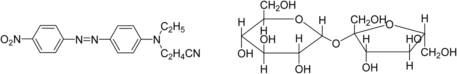 | ||
| Fig. 56 Molecular structures of orange dye (OD) and sugar (disaccharide). | ||
Mandal et al. designed a low voltage (<2 V) flexible OFET with high carrier mobility, employing gelatin as a moisture-induced ionic gate dielectric system.213 Low operating voltage OFETs are desirable in many applications because the typically available output voltage of batteries is only about 2 V.214 Hence, for wearable electronics, the OFETs with an operating voltage higher than 2 V are not suitable. In this work, a bilayer dielectric system was developed for overcoming the shortcomings of the ionic liquid for the fabrication of OFETs and to produce high carrier mobility at low voltage (Fig. 57). One of the components of the dielectric system was protein (gelatin), which produced protons in the presence of the absorbed ambient humidity and acted like an ionic solid. Protein (gelatin) in the presence of water generated protons unlike ion gels containing ionic components embedded in the composite dielectric. These protons were more mobile than ions inside the solid dielectric film. Consequently, the dielectric layer became ionic. Produced as a result of the water absorption, these extra charges magnified the charge accumulation in the dielectric/semiconductor interface and enhanced the device current. The second dielectric component of this bilayer system was a thin layer of Al2O3, which was used for reducing the operating voltage and the leakage current. The relative humidity dictated the ionic concentration in the gelatin layer during the measurements. The frequency of the capacitance measurement controlled the capacitance of the dielectric layer, which was used for the calculation of the carrier mobility for the OFETs. The results of the frequency-dependent gate capacitance along with the anomalous bias stress effect was used for the determination of the exact frequency, at which the carrier mobility should be calculated. The observed carrier mobility of the devices was found to be 0.33 cm2 V−1 s−1 with the capacitance measured at a frequency of 20 mHz. It could be overestimated to 14 cm2 V−1 s−1 with the capacitance measured at 100 kHz. The OFET devices were employed as highly sensitive humidity sensors. About three orders of magnitude variation in the device current was observed on the changes in the relative humidity levels from 10% to 80%. The devices displayed the response and recovery times of ∼100 and ∼110 ms, respectively. The devices were flexible up to a 5 mm bending radius.
 | ||
| Fig. 57 (a) Flexible device structure and (b) schematic diagram of the flexible device (reproduced with permission from ref. 213. Copyright 2020, ACS). | ||
Zafar et al. investigated the feasibility of the spin-cast poly(3,4-ethylenedioxythiophene)/poly(4-styrene sulfonate) (PEDOT:PSS)-based BGBC OFETs towards humidity sensing.215 The PEDOT:PSS was employed as a humidity sensing layer due to its porous and nano-fibrous surface morphology, which was believed to facilitate the adsorption/desorption kinetics of humidity inside the sensing film (Fig. 58). Initially, the water contents must arrive at the environment/semiconductor and then reach the semiconductor/gate dielectric interface to polarize into hydronium (H3O)+ and hydroxide (OH)− ions. These charges interacted electrochemically and/or electrostatically at the semiconductor/dielectric interface when VGS was applied, thereby modulating the current between the source and drain electrodes, as shown by eqn (3).
| H2O + H2O ⇔ H3O+ + HO− | (3) |
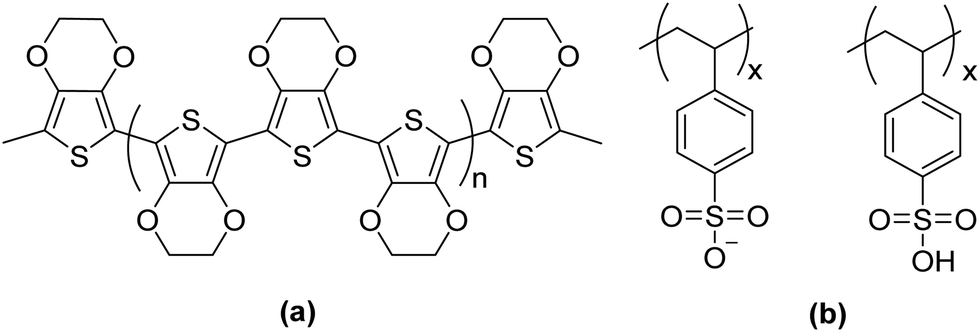 | ||
| Fig. 58 Chemical structures of (a) poly(3,4-ethylenedioxythiophene) and (b) poly(styrene sulfonate) polymer, referred as PEDOT:PSS. | ||
Biswas et al. reported a p-channel OFET-based humidity sensor containing polyaniline OSC (Fig. 59).216 The saturation current (ISat) of the OFET device was found to be 0.8 μA, while the threshold voltage Vth was 2.2 V. The fabricated sensors exhibited better response in the RH% range of 45 to 75, and displayed good reversibility with the increase and decrease in humidity. The drain current showed increasing tendency with the increase of the relative humidity up to 75% (at room temperature and VGS = −1 V). However, beyond that limit, the drain current drastically decreased with the increase of the relative humidity. With the RH beyond the limit of 75%, the relative response was continuously degraded. The temperature decreased at higher values of relative humidity. However, the relative humidity was inversely proportional to temperature. As the air becomes warmer, it could not hold more moisture. Thus, the percentage of the potential humidity decreased.
 | ||
| Fig. 59 Structure of the polyaniline semiconductor. | ||
Data related to the device design and performance of OFET-based humidity sensors have been summarized in Table 23.
| OFET's configuration | OSC/active layer | Dielectric layer | Additional layer/segment | Device performance | Ref. |
|---|---|---|---|---|---|
| TGBC | Pentacene | Parylene | — | • Increased subthreshold current was observed after 25% of RH, for 10–90% of humidity | Erouel et al.211 |
| BGBC | Orange dye + sugar (disaccharides) | Al2O3 | — | • Response time = 11 s | Karimov et al.212 |
| • Recovery time = 32 s | |||||
| BGTC | Pentacene | Gelatin + Al2O3 | — | • Mobility = 0.33 cm2 V−1 s−1 | Mandal et al.213 |
| • Response time = ∼100 ms | |||||
| • Recovery time = ∼110 ms | |||||
| • Flexibility = up to a | |||||
| 5 mm bending radius. | |||||
| BGBC | Poly(3,4-ethylenedioxythiophene)/poly(4-styrene sulfonate) (PEDOT:PSS) | SiO2 | — | • With the increase in relative humidity from 40 to 80%, the drain current increased 29.4 times | Zafar et al.215 |
| • Ion/Ioff = ∼2.6, under RH of ∼60% | |||||
| BGTC | Polyaniline | SiO2 | — | • Sensors showed better response in the RH% range of 45 to 75 | Biswas et al.216 |
| • Good reversibility with increased and decreased humidity | |||||
| • With RH beyond 75%, relative response was degraded continuously |
2.8. Biosensors
The highly sensitive and reliable determination of biological analytes plays a crucial role in the timely diagnosis, monitoring and treatment of diseases. A biosensor is an analytical device that incorporates biological recognition elements, converting a biorecognition event into a processable and quantifiable signal with the aid of a transducer.217 These biosensors are vital components in many domains, especially in personalized health and fitness, clinical laboratories, food and the environment. Currently, focused areas of research include designing self-contained, patient bedside sensors or so-called Point-of-Care sensors.218–220 These portable devices are supposed to provide fast and reliable analytical quantification of biomarkers right at the place where they are most needed.OFET-based biosensors have attracted a great deal of attention due to the advantages they offer, including convenient preparation over a large area, low cost, miniaturization, fast response speed and biocompatibility.26,221–223 The fundamental principle of OFET-based biosensors implies the modulation of the electrical characteristics of the semiconductor based on the attachment of biological analytes to the surface of a transistor. The output of the transistor changes by this modification, enabling the measurement and correlation with the biological analyte's concentration present in the sample. Over the years, researchers have adopted a variety of strategies for designing and constructing innovative types of sensors for the improvement of bioassay capability of OFET-based biosensors. While OFETs based on solid dielectrics have garnered attention as sensors over the past several decades,224 electrolyte-gated OFETs are a relatively new class of bioelectronic sensors. EGOFETs possess the biocompatibility and ability to detect analytes in complex matrices such as serum and inherently gain amplification with a direct read-out, making them highly desirable for biosensing.43,225–228 Label-free immunosensors, exploiting an organic semiconductor channel as the transducer of the biorecognition events, are emerging as highly specific and ultrasensitive devices for bioanalytical assays, with figures of merit that are often comparable or sometimes even superior in comparison to those characterizing the workhorse of bioanalytical techniques. Organic biosensors offer the following important advantages as compared to the label-free electronic sensors based on inorganic semiconductors, such as chemical field-effect transistors (CHEM-FETs)229 and metal-oxide field-effect transistors (MOSFETs):230 (i) the stability of operations in aqueous electrolytes; (ii) the closer proximity with the aqueous environment, as the organic semiconductor channel is immersed in the biologically relevant fluid; and (iii) the possibility to be interfaced or integrated as arrays with living systems.
Seshadri et al. reported a label-free immunosensor based on EGOFET for detecting procalcitonin (PCT), which is a sepsis marker.231 Antibodies specific to PCT were immobilized on the poly-3-hexylthiophene (P3HT) OSC surface via direct physical adsorption (Fig. 60). This was followed by a post-treatment with bovine serum albumin (BSA), which served as the blocking agent for preventing nonspecific adsorption. Antibodies along with BSA (forming the whole biorecognition layer) acted to selectively capture the PCT target analyte. The entire immunosensor fabrication process required a total of 45 min for completion before analyte sensing. The LOD of the immunosensor was as low as 2.2 pM and within the range of clinical relevance. The relative standard deviation of the individual calibration data points, measured on immunosensors fabricated on different chips (reproducibility error), was below 7%. The EGOFET immunosensor exhibited excellent electrical properties, comparable to those of bare P3HT based EGOFET and displayed high selectivity to the PCT analyte.
 | ||
| Fig. 60 Schematic representation of the developed EGOFET immunosensor for PCT detection. The anti-PCT antibody was directly adsorbed on the P3HT surface (panel 1), followed by surface blocking with BSA to reduce the nonspecific interaction (panel 2). The constructed immunosensor is exposed to the analyte (panel 3) and the electrical response is measured. (single column) (reproduced with permission from ref. 231. Copyright 2018, Elsevier). | ||
Ricci et al. developed a label-free sensor based on an electrolyte-gated OFET (EGOFET) integrated with microfluidics that allowed for the detection of amounts of α-synuclein in the range from 0.25 pM to 25 nM.232 α-Synuclein is a small protein made up of 140 amino acids (19–20 kDa), which, in its pathological condition, is a component of the so-called Lewy Body inclusions. The aggregation of α-synuclein is a critical event in the pathogenesis of neurological diseases, including Alzheimer and Parkinson. In EGOFET, the gate electrode was the effective sensing element, as it was functionalized with anti-(α-synuclein) antibodies using a dual strategy (Fig. 61). Anti-(α-synuclein) antibodies (Abs) were tethered on the polycrystalline Au by means of two different approaches. Approach I relied on an amino-terminated pegylated thiol (HSC11EG6NH2), whose amino groups were successively activated with glutaraldehyde (Gl). This resulted in the functionalized Au being highly reactive towards primary amines, which were quite abundant in the antibodies backbone. Approach II did not covalently graft the antibody to the surface but tethered it to the His-tagged recombinant Protein G (PG), which was anchored to the Au. PG efficiently targeted the crystallizable antibody region. Both of these protocols resulted in achieving comparable sensitivity values, featuring very low LOD values at the sub-pM level.
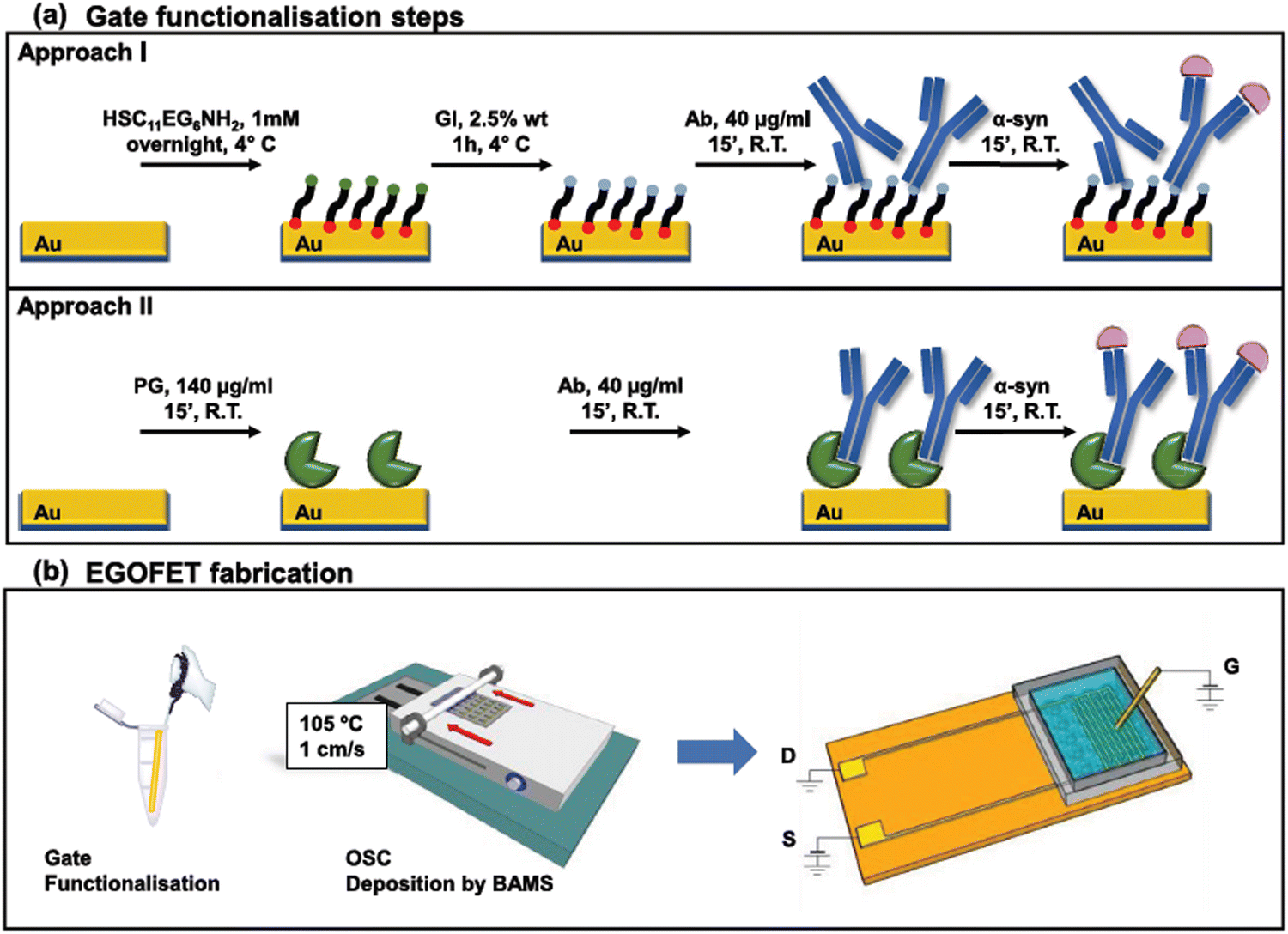 | ||
| Fig. 61 (a) Scheme of the Au surface functionalization protocol with Approach (top) I and (bottom) II. (b) Scheme of the EGOFET fabrication, including the gate functionalization, organic semiconductor deposition and the EGOFET implementation (reproduced with permission from ref. 232. Copyright 2020, Elsevier). | ||
Berto et al. reported a bioelectronic Plum Pox Virus (PPV) biosensor based on EGOFET for specifically detecting PPV with a sub ng mL−1 detection limit in plant extracts.233 PPV is the pathogen responsible for the Sharka, which is a highly infectious disease that is responsible for damaging stone fruit trees. EGOFETs were endowed with immunorecognition upon functionalization of surfaces located at one of their relevant interfaces. Recognition moieties were immobilized at the gate/electrolyte interface for exploiting facile thiol–gold chemistry (Fig. 62). The sensing unit of the biosensor was based on uniformly oriented anti-PPV antibodies on the gold gate electrode by employing a sub-monolayer of Protein G. Protein G served as a primer for further grafting the antibody on the surface with a precise orientation, owing to its high affinity for the heavy chain of Immunoglobulins G. Protein G was covalently bound to the Au, exploiting a single surface exposed engineered Cys residue. Changes in the drain current were observed mainly due to transconductance changes upon binding of the PPV to the surface immobilized antibody, while biorecognition had minimal effect on the threshold voltage. This finding suggested that the biosensor response was dominated by changes in the capacitance. By constructing a calibration curve based on transconductance changes as a function of the PPV concentration, a theoretical LOD of 180 pg mL−1 was estimated and operated the biosensor within a dynamic range spanning four orders of magnitude from 5 ng mL−1 to 50 μg mL−1. The sensitivity and dynamic range of the EGOFET-based biosensor were comparable to those of commercially available enzyme-linked immunosorbent assay (ELISA) platforms for detecting plant pathogens.
 | ||
| Fig. 62 Schematic experimental setup with the highlighted source, drain, and gate electrodes, the organic semiconductor layer on the quartz substrate, the electrolyte and the electrical connections (left). On the right is a zoom-in view of the functionalization strategy: PPV antibodies are immobilized on the gate surface through covalent binding of protein G, exploiting a single surface exposed Cysteine (reproduced with permission from ref. 233. Copyright 2019, Elsevier). | ||
Poimanova et al. reported that the biosensitivity of the EGOFET devices could be achieved by modifying the receptors of the electronically active OSC surface of transistor.234 Functionalization of the OSC layer was advantageous in the creation of a planar architecture and compact devices for lab-on-chip design. A fast and simple technique was proposed based on Langmuir–Schaefer and doctor blading methods for functionalization of the semiconducting surface of 2,7-dioctyl[1]benzothieno[3,2-b]-benzothiophene (C8-BTBT-C8). This allowed the fabrication of a large-scale biorecognition layer based on the novel functional derivative of BTBT-containing biotin fragments, 5-[(3aR,4R,6aS)-2-oxohexahydro-1H-thieno[3,4-d]imidazol-4-yl]-N-({1-[6-(7-undecyl[1]-benzothieno[3,2-b][1]benzothien-2-yl)hexyl]-1H-1,2,3-triazol-4-yl}methyl)pentanamide (BTBT−biotin) as a foundation for further biomodification (Fig. 63). The fabricated devices were very efficient and operated stably in phosphate-buffered saline solution with high reproducibility of the electrical properties in the EGOFET regime. The development of the biorecognition properties of the proposed biolayer was based on the streptavidin (SA)–biotin interactions between the consecutive layers, and could be used for a wide variety of receptors. The responses of the sensor to different SA concentrations upon changing the Vth of EGOFETs without (0% biotin) and with the bioreceptor layer (30% BTBT–biotin) were measured. The responses of the device with bioreceptor layers was linear in the region of the SA concentration from 6 to 50 μg mL−1, while it leveled off at the concentration of 50 to 200 μg mL−1 within the experimental error. The LOD of SA was found to be 3 times the standard deviation (over 10 replicates) of the response and it was equal to 6 μg mL−1. All of the devices displayed very low degradation and reproducible electrical characteristics.
 | ||
| Fig. 63 Illustration of the fabrication process of the (c) EGOFET device with BTBT−biotin containing a biorecognition layer by means of combination of the (a) doctor blading and (b) Langmuir−Schaefer techniques (reproduced with permission from ref. 234. Copyright 2022, ACS). | ||
Kyndiah et al. reported on EGOFETs based on a solution processed small molecule, 2,8-difluoro-5,11-bis(triethylsilylethynyl)anthradithiophene (diF-TES-ADT) blended with polystyrene for recording the extracellular action potentials of human pluripotent stem cells-derived cardiomyocyte cells (hPSCs-CMs).235 hPSCs-CMs are known as a powerful tool in cardiac biology for cardiac disease modelling. The functionality of these EGOFETs remained unaltered when an extracellular matrix such as Matrigel (commonly employed for attaching cells) was coated on top of the transistors (Fig. 64). These sensing devices displayed excellent stability in physiological conditions over weeks with an almost negligible decrease in the charge carrier mobility (less than 1 order of magnitude) and with a shift of below 0.1 V in the threshold voltage. The stability of these devices was attributed to the smoothness and high crystallinity of the films deposited by the shearing technique BAMS.236 Additionally, cytotoxicity tests of pharmaceutical drugs, such as verapamil and norepinephrine were achieved with remarkable sensitivity.
 | ||
| Fig. 64 Schematic diagram of the EGOFET coupled to hPSCs-CMs grown as a cluster of cells (reproduced with permission from ref. 235. Copyright 2020, Elsevier). | ||
Poimanova et al. reported on EGOFETs based on the semiconducting material, 2,6-dioctylthieno[3,2-b]thieno[2′,3′′:4,5]thieno[2,3-d]thiophene(2,6-dioctyltetrathienoacene) (C8-TTA-C8) and the biorecognition layer based on the biotin-containing derivative of [1]benzothieno [3,2-b]-benzothiophene (C8-BTBT-C8) (Fig. 65).237 These devices displayed stable operation in electrolytes under different pH values and a fast sensor response to the electrolyte pH value, which allowed one to use these devices under actual conditions. This was critical to the development of liquid biosensors. This study demonstrated that biosensing properties could be imparted to EGOFETs by coating the semiconductor surface with the biorecognition layer containing biotin functional groups acting as reactive sites for the biotin–streptavidin interaction.
 | ||
| Fig. 65 Chemical structures of the compounds C8-TTA-C8 and C8-BTBT-C8. | ||
Sun et al. developed label-free single molecule level determination with a transistor (SiMoT) platform for the recognition of various ultralow abundance biomolecules (Fig. 66).238 Pillar[5]arene with carboxylic groups, (DMP[5]-COOH), was integrated as a signal amplifier, which was later used for efficient immobilization of antibodies as sensitive probes. DMP[5]-COOH is rich in host–guest chemistry and has efficiently recognized various target analytes. Pillar[n]arene, a new type of macrocyclic host, is also rich in host–guest chemistry and the electron-rich cavities in pillar[n]arene not only specifically recognized various target analytes, but also provided suitable reaction sites by modifying functional groups. The sensitivity was greatly improved with the integration of DMP[5]-COOH in a certain ratio and the detection limit reached 4.75 aM. Afterward, the OFET-based SiMoT platform was separated into different areas and the multibiomarkers, carcinoembryonic antigen (CEA), α-fetoprotein (AFP) and prostate antigen (PSA) were determined simultaneously, which indicated that this proposed multiplexed OFET-based SiMoT platform could provide a key step in reliable early cancer diagnosis. In order to guarantee that the OFET-based SiMoT platform could also be applied in the clinical diagnosis, 1 ng mL−1 of AFP, 1 ng mL−1 of CEA, and 1 ng mL−1 of PSA were reacted with the sensing areas, and the specific response values of ΔVth under different conditions were 2.32 ± 0.155 V on anti-AFP, 4.21 ± 0.425 V on anti-CEA, and 1.72 ± 0.113 V on anti-PSA, respectively. As compared to the blank control response to phosphate buffer solution (1× PBS), 0.51 ± 0.216 V on anti-AFP, 0.53 ± 0.101 V on anti-CEA, and 0.33 ± 0.031 V on anti-PSA, the results proved that the OFET-based SiMoT platform could achieve simultaneous determination of AFP, CEA, and PSA below the cut-off value (AFP = 10 ng mL−1, 32 CEA = 2.5 ng mL−1, 33 PSA = 2.5 ng mL−1, 34), so as to improve the accuracy of cancer screening in early cancer diagnosis.
 | ||
| Fig. 66 The schematic representation of the OFET-based SiMoT platform. Step 1: the PDBT-co-TT/DMP[5]-COOH was spin-coated as the charge transport layer on the OTS-modified SiO2/Si substrate with the deposited Au source and drain electrodes; step 2: the antibodies were immobilized as sensitive probes for the determination of tumor biomarkers; step 3: the antibody-antigen recognition events (reproduced with permission from ref. 238. Copyright 2022, ACS). | ||
Wang et al. developed an OFET-based biosensor using diketopyrrolopyrrole-quaterthiophene as the OSC material for the carcinoembryonic antigen (CEA) bioassay.239 This biosensor responded sensitively to the antigen–antibody immune-recognition reaction under darkness and illumination conditions, thus generating electrical signal changes of Vth and IDS. The detection limits for CEA detection of 0.5 and 0.2 pM, respectively, were determined using IDS and Vth as the response signals under darkness. Light would influence the charge-carrier transport process in the conductive channel when a specific intensity of light was applied, resulting in the biosignals turning into higher electrical signal changes of Vth and photocurrent under illumination. The biosensor displayed higher sensitivity for CEA detection under illumination with detection limits of 13.5 and 16.9 fM, as compared to the detection results under dark conditions. The protein was negatively charged, when the pH of the solution exceeded the isoelectric point (pI) of the protein since the pI of CEA was 3.40, which was lower than the pH value of the solution (∼7.40). Consequently, when an antigen–antibody immune reaction occurred to form an immune complex, more negatively charged proteins were attached to the biosensing layer, thus promoting the generation of more carriers in the conductive channel because of electrostatic interaction. The binding of negatively charged CEA with receptors on the semiconductor surface would cause the threshold voltage to move in a positive direction and the source–drain current of the organic device to increase under dark conditions (67a). When the p-type OSC with photoelectric activity was employed as the semiconductor layer of OFET, the excitons in the conductive channel dissociated to produce photogenerated carriers when a certain intensity of light was applied to the OFET (Fig. 67b). Driven by the internal electric field, electrons and holes accumulated at the source electrode and the drain electrode, respectively, causing the reduction of the hole-injection barrier at the interface between the electrode and the conductive channel, thus indicating the higher channel conductivity (Fig. 67c). Illumination caused the trapped holes in the channel to escape from the trap and rejoin the carrier-transport process to increase the carrier concentration caused by biological combination, increasing the IDS and shifting Vth towards the positive direction, thus improving the detection sensitivity (Fig. 67).
 | ||
| Fig. 67 Mechanism of the OFET-based biosensor under illumination and darkness: (a) working principle of the OFET-based biosensor for the detection of CEA in the dark, (b) generation of photogenerated carriers of the OFET-based biosensor under light illumination, (c) movement of photogenerated carriers in the electric field, (d) working principle of the OFET-based biosensor for the detection of CEA under illumination (light source = 2.13 mW cm−2, 808 nm) (reproduced with permission from ref. 239. Copyright 2021, ACS). | ||
Yousefi et al. reported on an OFET-based biosensor for detecting protein–protein interactions (PPIs).240 This sensory platform was tested by employing a pair of interacting proteins, which were stable with reasonably high binding affinity, preferably in the low nanomolar range and formed a 1:1 complex with a known binding site (Fig. 68). Deubiquitinase (DUB) enzyme ubiquitin-specific protease 8 (USP8) and its cognate ubiquitin variant inhibitor UbV8.2 were selected as a model system for testing and validating the sensing ability of these biosensors. DUBs are enzymes critical for maintaining protein homeostasis in cells, and their deregulation can result in many diseases. Poly-(diketopyrrolopyrrole-co-thienovinylthiophene) [P(DPP-TVT)]-based semiconducting polymer was employed in an OFET sensing device on which an epoxyterminated monolayer, (3-glycidoxypropyl)trimethoxysilane (GPTMS), was deposited for protein immobilization. UbV8.2 was immobilized covalently on the device for functioning as the bait, and for creating a functionalized channel to detect the presence of the prey that is USP8. The fabricated sensors depicted a LOD of 0.22 nM (0.01 μg mL−1). These devices were only responsive to USP8 when UbV8.2 was immobilized as the bait. These results suggested that the covalent immobilization of UbV8.2 and the sensor surface have a small impact on the protein structure or orientation necessary for molecular recognition by USP8.
 | ||
| Fig. 68 Schematic of the (a) fabricated bottom-gate top-contact OFET with chemical structures of the semiconducting polymer layer [P(DPP-TVT)] and functionalized layer (GPTMS). (b) Diagram of the device surface after bait protein immobilization and prey protein binding. The top gold electrodes are omitted for clarity (reproduced with permission from ref. 240. Copyright 2022, ACS). | ||
Domingo et al. proposed an organic inkjet-printed TGBC BioFET structure using a perfluoropolymeric material Cytop™ as both the gate insulator and the transducing layer.241 Perfluoropolymers possess interesting characteristics, such as low water absorption and high electrical breakdown. The weak dispersive interactions of fluorocarbons, dipolar cancellation and lack of polarizability that were conferred by C–F bonds in perfluorocarbon compounds made them a good choice for top-gate OFET and BioFET applications. The OSC was not directly exposed to the sensing environment as it was protected by the dielectric, which was in direct contact with the medium to be analyzed (Fig. 69). The bio-recognition element was anchored onto the dielectric surface, which acted as the sensing area. This configuration ensured field-effect operation without charge transfer between the electrolyte and the OSC, blocking the passage of the current, which could promote electrochemical reactions such as hydrolysis. The immobilization of the receptors onto the insulator by covalent bonding was achieved using a simple approach involving a model protein. The main advantage of the proposed method was that no specialized equipment was needed, so it could be conducted in most laboratories. The detection of the model antigen HIgG was conducted as a proof-of-concept, showing that the developed procedure could be used in immunosensing analysis. These BioFETs operated at threshold voltages in the range of 1–2 V, detecting the HIgG with a LOD of 5.71 μg mL−1 with good reproducibility and selectivity. These devices displayed durability even when exposed to oxygen plasma, aqueous media and wet amine functionalization treatments.
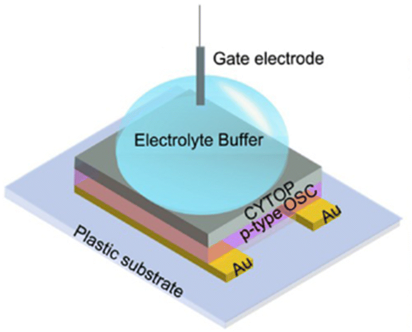 | ||
| Fig. 69 Optical image of the electrical characterization setup of the top-gate BioFETs (reproduced with permission from ref. 241. Copyright 2020, Elsevier). | ||
Sun et al. designed an ultrasensitive OFET-based biosensor modified with 2,6-bis(4-formylphenyl)anthracene (BFPA) materials, and employed it to determine the concentration of alpha-fetoprotein (AFP) biomarkers with femtomolar accuracy in human serum for the diagnosis of early liver cancer.242 This device displayed improved reliability in sensing the AFP biomarker by monitoring changes of the IDS and Vth electrical signals, and distinguished between healthy individuals and liver cancer patients. BFPA materials were used for maintaining device performance as the protective layer and efficiently immobilized antibody receptors as the functional layer (Fig. 70). The average carrier mobility was 0.18 cm2 V−1 s−1, with a maximum hole mobility of 0.24 cm2 V−1 s−1. The output electrical signals were affected by biochemical reactions between antigens and antibodies before transduction, and then amplified by this biosensor. Electrical output responses were strongly dependent on protein charges at different pH values. Particularly, the isoelectric point (pI) of the AFP biomarker occurred at 4.9. There is a high density of COO− in the anti-AFP/AFP complex at pH values higher than the pI, causing weak electrostatic interactions between the surface charges and channel region. Therefore, there is a notable negative shift in the Vth electrical signal and decrease in the IDS electrical signal. The decrease in IDS was attributed to depleted holes in the channel region, resulting from higher levels of negative charges acting as channel traps, making the device harder to turn on and causing Vth shifts to a negative direction. The charge screening effects were expected to take place when detecting charges that exceed the Debye length (λD).243 In this study, notable charge screening effects might occur at short λD = 0.7 nm in 1× PBS as the AFP antigen and antibody interactions needed salts for maintaining bond stability.244 The Donnan effect was proposed for further guaranteeing the effective detection.229 In this, proteins were considered as a charged molecule layer on the device and small ions could shuffle between the proteins and 1× PBS. The redistribution of ions at the interface resulted in a detectable change in the interfacial potential, following the incubation of biomarkers. Thus, biomolecules could then be detected through surface-charge sensing devices such as OFET.
 | ||
| Fig. 70 (a) Schematic representation of the OFET-based biosensors; (i) fabrication of the OFET-based biosensors; (ii) Au source and drain electrodes are deposited; (iii) PDVT-8 film is spin-coated as the charge transport layer; (iv) and (v) BFPA functional layer is modified on the device as the functional layer; (b) AFP antibodies are immobilized to form the receptor layer for the determination of the target AFP biomarkers; (iii) schematics showing surface modification; (iv) to immobilize antibodies as receptors; (v) for the determination of the target AFP biomarkers (reproduced with permission from ref. 242. Copyright 2021, ACS); (c) chemical structure of the organic molecules (BFPA and PDVT-8). | ||
Li et al. reported on water stable transistors based on naphthodithieno[3,2-b]thiophene derivatives NDTT-8 and NDTT-10, with two long alkoxyl side chains.245 Excellent water stabilities were displayed by the devices based on NDTT derivatives. Continuous monitoring of the device performance was performed under constant conditions, in which the devices were kept under three different experimental conditions, including water, water vapor and air (Table 24). The carrier mobility was maintained at more than 50%, even after 90 days in water. The long hydrophobic alkoxyl chains in NDTT-8 and NDTT-10 molecules were responsible for better water stabilities of their OFET by effectively preventing water from spreading to the interface between the OSC layer and the insulating layer (Fig. 71).
| R total·W (kΩ cm) | NDTT-8 | NDTT-10 | Pentacene | PDVT-10 |
|---|---|---|---|---|
| As-prepared | 17.5 | 22.4 | 14.9 | 5.3 |
| Air | 78 | 71 | 24 | 9.8 |
| Water vapor | 71 | 92 | 36 | 7.1 |
| Water | 85 | 99 | 23.7 | 10 |
 | ||
| Fig. 71 Molecular structures of the organic semiconductors NDTT-8, NDTT-10, PDVT-10 and pentacene. | ||
Macchia et al. proposed a highly selective, label-free sensing response of a single molecule with a large transistor (SiMoT) platform toward genomic biomarkers.246 These SiMoTs were based on an electrolyte-gated FET with a gold gate electrode bio-functionalized with a self-assembled monolayer, a densely packed layer of recognition elements (Fig. 72). Until the publication of this work, the SiMoT platform had been employed for the detection of only protein biomarkers such as C-reactive protein, human immunoglobulin G, immunoglobulin M and HIV1 p24 antigen. In this study, the SiMoT approach was successfully employed for detecting a single copy of a genomic biomarker. The miR-182 biomarker for multiple sclerosis was chosen as a prototypical example. The gate was functionalized with a genomic biomarker for multiple sclerosis (miR-182). The bioprobe was attached on the gate surface instead of attaching it on the surface of OSC to elude the generation of defects in the delocalized electronic system, affecting the charge carrier mobility. Furthermore, the SiMoT device exploited solution-processable semiconducting device fabrication protocols that were fully compatible with scalable large area and printing techniques. The SiMoT sensing platform could detect both genomic and protein markers at the physical limit, and a LOD level of 7% was estimated.
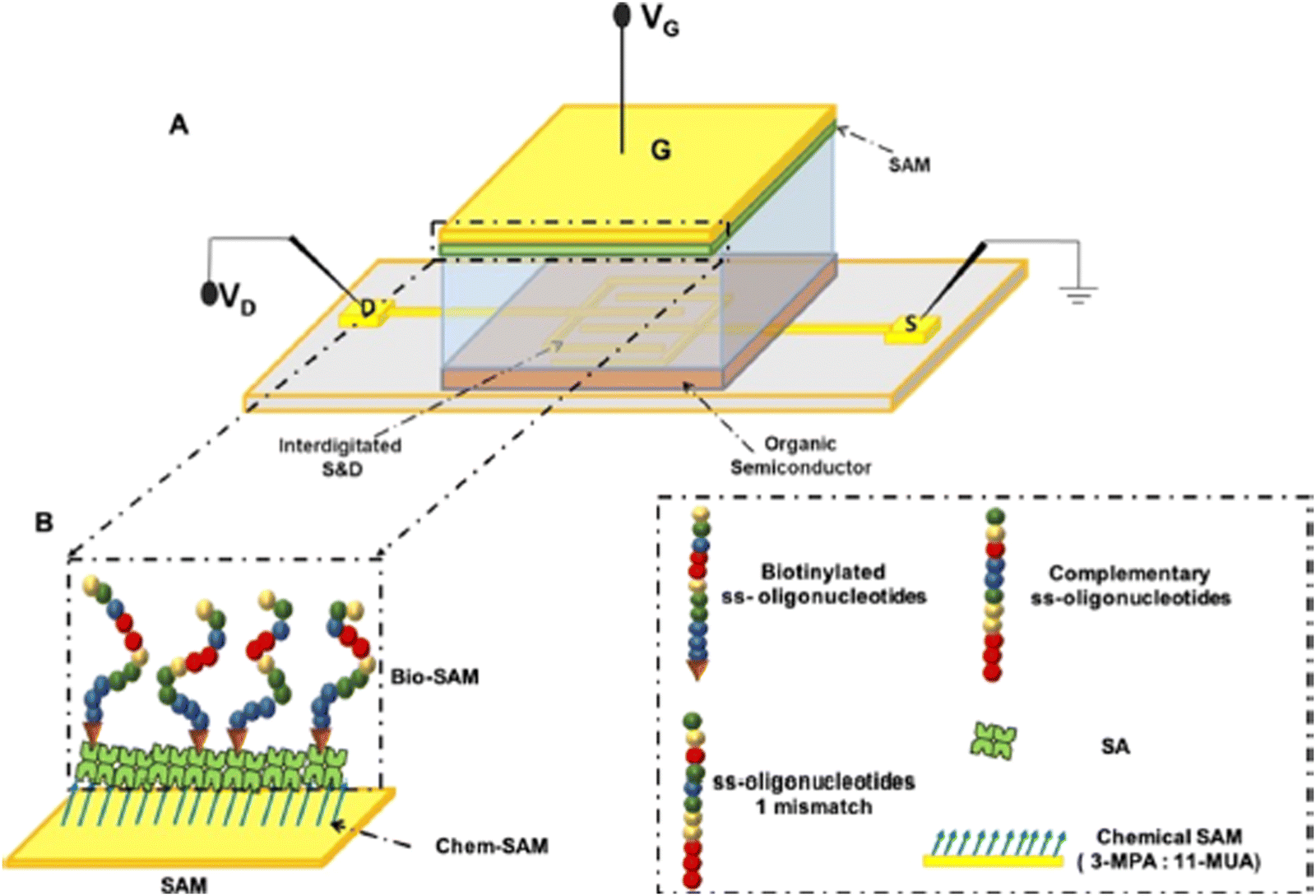 | ||
| Fig. 72 (A) Three-dimensional schematic representation of the SiMoT device. (B) Schematic representation of the gate surface biofunctionalized with a biotinylated single-strand oligonucleotide. Chem-SAM is depicted by blue arrows, and the structures of the bio-SAM and target oligonucleotides (miR-182-5p) are sketched in the right panel (reproduced with permission from ref. 246. Copyright 2020, ACS). | ||
Dey et al. exploited the charge density on the bacterial cell wall to influence the charge density in OFETs, thereby providing authentic mechanistic signals and useful information regarding bacteria-probe interaction.247 A low voltage, n-type OFET was fabricated using a hybrid tri-layer (Al2O3/TiO2/PMMA) dielectric system for the label-free detection of Gram-positive and Gram-negative bacteria (Fig. 73). Each dielectric layer in the device architecture had a significant contribution towards building an efficient bacteria sensor device by decreasing the operational voltage of N,N-dioctyl-3,4,9,10-perylenedicarboximide (PDI-C8)-based OFET. This device provided rapid and multiple measurable signals with enhanced accuracy of measurement, in addition to providing mechanistic insights on the process of bio-analyte detection in water. For the accurate bacterial sensing, it was crucial to determine the interaction between the charge carriers in the channel and the surface of the bacterial cell wall. In the presence of Gram-negative bacteria, the average μe decreased from 0.3 cm2 V−1 s−1 to 0.2 cm2 V−1 s−1 with increased Vth from 0.2 V to 0.5 V, while the average μe increased from 0.3 cm2 V−1 s−1 to 0.5 cm2 V−1 s−1 with reduced Vth (0.2 V to −0.5 V) in the presence of Gram-positive bacteria. This was the first report of an OFET-based detection of bacteria, providing a clear ability of distinguishing the bacteria types and having detection limit of 103 cfu per mL for Gram-negative and Gram-positive bacteria with a low operating voltage of ∼2 V. These devices were fabricated using low-cost glass and PET substrates without using ITO or/and Si/SiO2. The device parameters of the bacteria sensors are summarized in Table 25.
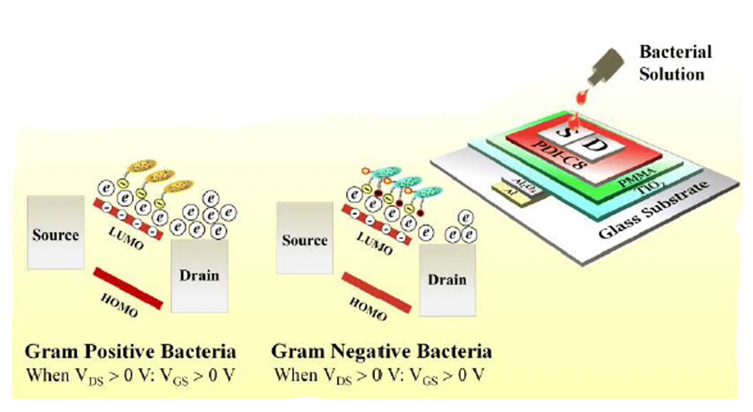 | ||
| Fig. 73 Operational mechanism of the same device in the presence of Gram-positive and Gram-negative bacteria in the channel (reproduced with permission from ref. 247. Copyright 2019, RSC). | ||
| With/without bacteria | V th (V) | μ (cm2 V−1 s−1) | I on/Ioff ratio | Limit of detection (LOD) CFU per mL | |
|---|---|---|---|---|---|
| Bare | — | 0.20 (±0.03) | 0.30 (±0.02) | 104 | — |
| With Gram-positive bacteria | 439 | −0.50 (±0.04) | 0.50 (±0.03) | 105 | 2.3 × 10³ |
| 1305 | −0.47 (±0.03) | 0.52 (±0.04) | 105 | 2.7 × 10³ | |
| With Gram-negative bacteria | 2488 | 0.49 (±0.02) | 0.21 (±0.03) | 103 | 2.4 × 10³ |
| DH5α | 0.52 (±0.03) | 0.22 (±0.02) | 103 | 2.8 × 10³ | |
Fang et al. fabricated a low-voltage organic inverter, namely complementary metal–oxide–semiconductor (O-CMOS) on flexible polyimide substrates for sensing S. aureus, E. coli, and E. faecalis.248 The active layers consisted of n-type N,N′-ditridecylperylene-3,4,9,10-tetracarboxylic diimide (PTCDI-C13) to serve as a bacterial sensor and p-type pentacene (Fig. 74). For enhancing the stability of the inverter's performance while reducing the potential effect of the bacterial culture liquid when introduced into the device, the cross-linked poly(4-vinylphenol) (C-PVP) was incorporated as an insulating layer. Bacteria were introduced into the inverter for investigating their effect on the carrier transport under the low voltage of 2 V. A summary of the electrical performances for PTCDI-C13- and pentacene-based OFETs is provided in Table 26. Different concentrations of bacteria were introduced into the n-type channel of the O-CMOS. The switching voltage offset of the O-CMOS, which could be read rapidly and directly, gradually decreased with a decrease in the bacterial concentration. The O-CMOS device reliably detected the presence of bacteria even when the concentration was decreased to approximately 102 CFU per mL, indicating its excellent sensitivity for rapid detection (Table 27).
 | ||
| Fig. 74 Structures of the OFETs and organic inverter (reproduced with permission from ref. 248. Copyright 2024, MDPI). | ||
| Organic semiconductor | Types of solutions | V th (V) | V th (V) (average value of five devices) | On/off current ratio | SS (V dec−1) |
|---|---|---|---|---|---|
| PTCDI-C13 | Non solution | 0.38 | 0.31 ± 0.39 | 1.37 × 10⁴ | 0.15 |
| DI water | 0.48 | 0.50 ± 0.38 | 1.27 × 10⁴ | 0.23 | |
| E. coli | −0.09 | −0.12 ± 0.21 | 7.85 × 10⁶ | 0.06 | |
| S. aureus | 0.06 | 0.19 ± 0.73 | 6.45 × 10⁵ | 0.11 | |
| E. faecalis | 0.28 | 0.07 ± 0.28 | 6.99 × 10⁶ | 0.08 | |
| Pentacene | Non solution | −0.68 | −0.56 ± 0.08 | 1.58 × 10⁴ | 0.37 |
| DI water | −0.44 | −0.30 ± 0.19 | 3.23 × 10³ | 0.46 | |
| E. coli | −0.31 | −0.39 ± 0.17 | 1.68 × 10³ | 0.69 | |
| S. aureus | −0.37 | −0.25 ± 0.71 | 8.51 × 10³ | 0.42 | |
| E. faecalis | −0.43 | −0.28 ± 0.51 | 4.01 × 10³ | 0.52 |
| Concentration of bacteria (CFU per mL) | ΔVS (V) | ||
|---|---|---|---|
| E. coli | S. aureus | E. faecalis | |
| 108 | 0.56 | 0.51 | 0.45 |
| 104 | 0.27 | 0.29 | 0.30 |
| 102 | 0.19 | 0.06 | 0.16 |
Chen et al. reported on remote-gate-configured OFET sensors for the label-free detection of vascular endothelial growth factor (VEGF), which is a critical biomarker associated with various diseases, including diabetic retinopathy, cancers and macular degeneration. This study offered a systematic comparison of their performance.249 The poly[3-(3-carboxypropyl) thiophene-2,5-diyl] (PT-COOH) transducer films on remote dual gates were functionalized with the VEGF aptamer (VEap), either alone or in conjunction with its complementary single-stranded DNA (PT-VEap vs. PT-VEap/CS) (Fig. 75). The single-stranded aptamer VEap, specific to VEGF121, was functionalized on the PT-COOH film surface using amidation, while CS DNA was engineered to form a double-stranded structure, regulating the conformation of VEap through base pairing. The single-stranded and double-stranded aptamer-based sensors displayed opposite changes in Vth in response to VEGF, and the contribution of CS pairing to signaling was evidenced by the lower detection limit of the PT-VEap/CS sensors (0.1 ng mL−1) as compared to that of PT-VEap sensors (1 ng mL−1). The PT-VEap sensors showed a faster response, while the PT-VEap/CS sensors provided reliable and more stable signals. Both sensors exhibited high sensitivity to VEGF across a broad pH range (5–9) and ionic strength (0.05–1.0× PBS), with a slight advantage for PT-VEap/CS in salt resistance and for PT-VEap in pH resistance.
 | ||
| Fig. 75 (a) Schematic of the remote dual-gated FET sensing system: the two remote gates are connected in parallel to the gates of the commercial transistor. (b) Functionalization of the PT-COOH film with probe VEap/CS to form the PT-VEap sensing surface on the remote gates using EDC/NHS chemistry. (Reproduced with permission from ref. 249. Copyright 2025, Elsevier.) | ||
This novel remote dual-gate architecture integrated commercial FETs, and was derived from charge-modulated FET sensors featuring a floating extended gate. This design achieved stable signal conversion through commercial FETs, and also eliminated errors induced by random potential drifts between the gates. The parallel connection of the two remote gates created double capacitive coupling instead of the conventional single coupling, ensuring that occasional errors in either remote gate do not compromise the signal integrity within the three-terminal system. The sensing mechanism was studied by analyzing the surface structural changes and their effect on field effect variations near the surface of the PT-based transducers. DNA strands are negatively charged in slightly acidic to alkaline solutions due to the ionization of the phosphate backbone. In the VEGF sensing on the PT-VEap surface (Process I in Fig. 76), the space between the PT surface and the farthest end of VEap could be likened to a plate capacitor. The charges stored in the equivalent capacitance remained unchanged when VEGF was bound to VEap, while the distance between the plates decreased. The natural electric field formed by VEap and PT in this region increased, according to the relationship E = U/d. Consequently, more positive charges were induced on the PT surface, which led to an increase in ERG. The aptamers in the VEap/CS probes were partially complementary and shaped with another ssDNA (CS), showing distinct interface response behaviors. The CS-confined aptamer had a higher affinity for its target VEGF than the base pairing interaction because of its chemical and spatial compatibility. This competitive advantage allowed VEap to dissociate from the double-stranded probe, bind to VEGF, and release the CS. In the VEGF sensing on the PT-VEap/CS surface (Process II in Fig. 76), the major change involved the significant departure of CS from VEap, which is much more pronounced than the configurational transformations in VEap itself. Consequently, the equivalent plate capacitor formed between PT and the end of probes experienced changes primarily in the stored charge quantity during the response process. According to equation E = Q·4πk/εS, it could be deduced that the natural electric field formed by PT and VEap decreased. This reduction in the surface electric field intensity on PT led to a decreased concentration of the induced positively charged carriers on the sensing surface, causing a decrease in ERG.
 | ||
| Fig. 76 Proposed mechanisms of VEGF responses on the PT-VEap (Process I) and PT-VEap/CS (Process II) as remote gates of the FET sensors. The primary change in Process I is attributed to the conformational folding of VEap upon VEGF binding, which reduces the separation distance between the plates of the model capacitor. The primary effect in Process II is attributed to the release of the CS along with VEGF binding to VEap, leading to a decrease in the charge stored in the model capacitor. (Reproduced with permission from ref. 249. Copyright 2025, Elsevier.) | ||
Verma et al. reported the growth mechanism of a mercury-sensing molecule, pyridine-end oligo-p-phenylenevinylenes (POPV), deposited on pentacene in a BGTC OFET configuration (Fig. 77a). These sensing molecules possessed a lone pair at the nitrogen atom in the pyridine end, which helped in the formation of a selective coordination with mercury ions (Hg2+) (Fig. 77b). The introduction of a thin layer of receptor molecules specifically binding with mercury atop the pentacene semiconductor facilitated its function as a sensing layer without impeding its functionality as an active layer.250 The surface doping of receptor molecules above OSC diffused through the grain boundaries, changing electronic properties. The device performance was affected upon exposure to the target species. The uniform, controlled growth of mercury-sensing molecules above the semiconductors enabled highly effective sensing devices. The deposition of thin films over OSCs could impede charge transport, warranting a comprehensive examination of the growth mechanisms that optimized the device performance. Surface roughening and smoothening processes significantly influenced the surface morphology, which is vital for effective sensing applications, as they modulate the surface characteristics impacting the performance of the sensing-device.
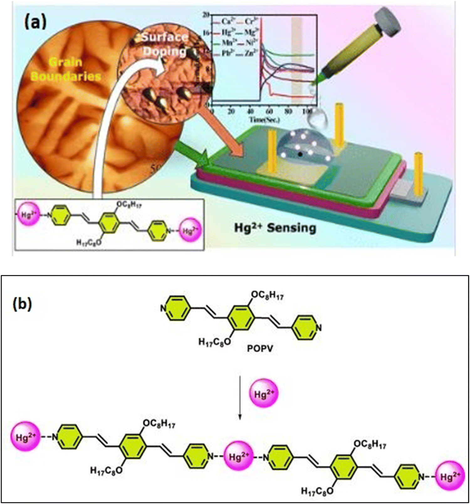 | ||
| Fig. 77 (a) Schematic design showing the visual representation of the OFET highlighting the arrangement of the various layers involved. (b) Molecular structure of the mercury-sensing molecule POPV forming a coordination complex with mercury. (Reproduced with permission from ref. 250. Copyright 2025, ACS.) | ||
Controlled samples of Zn2+, Ca2+, Cr3+, Ni2+, Mg2+, Mn2+, Pb2+, and Hg2+ salt solution nitrate (NO3−) as the counter ions were prepared. A droplet of 2 μL solution containing the analyte was deposited in the channel region of the device. Upon introduction of the solution, a notable direct ionic current was observed flowing from the source to the drain terminals. This current gradually decreased over time and eventually reached a saturation point. The selective binding of POPV with Hg2+ induced trap states, which reduced the charge carrier mobility and consequently lowered the conductivity compared to other ions. By examining how the drain current changed when the OFET was exposed to different ionic species, selectivity of the sensor toward its target ion, Hg2+ could be determined. This involved measuring the response of the drain current to different ions and comparing these responses to the response obtained from Hg2+ ions. The attainment of the smallest saturated drain current corresponded to the binding of Hg2+ with the pyridine-end oligomer, demonstrating the specificity of the sensing mechanism toward Hg2+ detection. This observation showed the effectiveness of the device in selectively detecting Hg2+ within the tested analyte solutions. The binding of Hg2+ ions with the surface molecules doped within the channel induced changes in the electronic properties, resulting in a decreased device current. In OFETs employing pentacene, where hole flow predominates, this reduction in the current suggested an increase in the electron supply to the channel due to the interaction between the molecules and Hg2+ ions. This selective interaction with Hg2+ ions is a vital factor in the device's ability to detect heavy metal ions in water with high specificity. The selective interaction between the Hg2+ ions and pentacene disrupted the hole conduction more effectively compared to other ions, which was crucial for achieving selectivity in ion detection. Consequently, a higher concentration of Hg2+ ions results in a lower device current.
Poimanova et al. demonstrated the possibility of quantitative, fast and specific determination of virus particles by an aptasensor based on electrolyte-gated OFET. Organosilicon BTBT-dimer and BTBT-C8 were employed as OSCs due to their stability in air and aqueous media (Fig. 78). The sensitivity and selectivity of the sensing devices were examined with the influenza A virus, as well as with control bioliquids like influenza B, Newcastle disease viruses or allantoic fluid with different dilutions.251 The high specificity of these sensing devices was proved by providing statistically significant dose-dependent signals in the concentration range of 6 × 10⁴–6 × 10⁸ viral particles per mL of the influenza A virus, which is on par with no interfering signals in the presence of off-target viruses (influenza B virus and virus of Newcastle disease) or virus-free biological fluid (allantoic fluid). The LOD of the influenza A virus of up to 6.1 × 10⁴ viral particles per mL was achieved for the device with the BTBT-dimer thin OSC layer, and up to 6.1 × 10⁵ viral particles per mL for the device with the C8-BTBT-C8 thick OSC layer. The influence of the OSC layer thickness on the sensory properties of EGOFETs was investigated. It was found that the device based on a single biotinylated bioreceptor layer without an OSC sublayer exhibited sensitivity to the influenza A virus, but it was poorly reproduced. Meanwhile, devices with both thin and thick active semiconducting layers and a biotinylated bioreceptor layer showed high sensitivity to the influenza A virus. The thinner organic semiconducting sublayer displayed a more intense signal (1.5 times higher) to the virus and an order of magnitude of greater sensitivity. The electrical parameters of the three types of investigated devices are summarized in Table 28. The fabrication of a multi-flow cell that simultaneously registered the responses from several devices on the same substrate was also reported. The responses of the elaborated bioelectronic platform to the influenza A virus obtained with application of the portable multi-flow mode were well correlated with the responses acquired in the laboratory stationary mode.
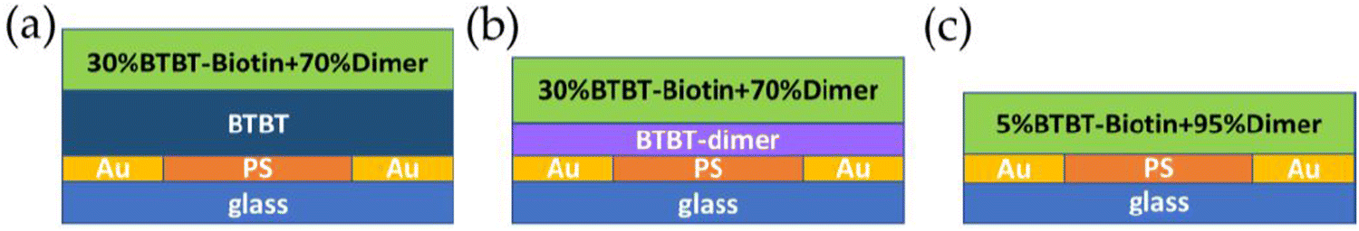 | ||
| Fig. 78 Architecture of the EGOFET-based biosensor devices manufactured with different OSC sublayers: (a) C8-BTBT-C8; (b) BTBT-dimer; (c) without any OSC sublayer. (Reproduced with permission from ref. 251. Copyright 2023, MDPI.) | ||
| Device | I on, μA | I off, μA | g m, A1/2 V−1(×106) | V th, mV |
|---|---|---|---|---|
| g m = the transconductance. | ||||
| C8-BTBTC8/biorecognition layer with 30%BTBT-biotin | −0.11 ± 0.02 | −0.01 ± 0.004 | −3.5 ± 0.5 | −215 ± 50 |
| BTBTDimer/biorecognition layer with 30% BTBT-biotin | −0.35 ± 0.05 | −0.05 ± 0.006 | −6.3 ± 0.7 | −235 ± 30 |
| Biorecognition layer with 5%BTBT-biotin | −0.10 ± 0.03 | −0.01 ± 0.005 | −3.4 ± 0.6 | −112 ± 20 |
Utsumi et al. reported the fabrication of an OFET sensor for the detection of urea hydrolysis under urease. A 2,6-diphenylanthracene (DPA) thin film was employed for the preparation of a p-channel FET that detected this enzymatic reaction (Fig. 79c). The absolute drain current, |ID|, of the transfer curve rapidly increased at any gate voltage, VG, when a droplet of 0.1 M phosphate buffer solution (pH = 6.7 at 25 °C) containing 25 mM urea and 49 nM urease was placed on a different gate electrode (i.e., sensor electrode) than the VG electrode.252 Thus, urea hydrolysis directly affected the value of VG, enhancing |ID|. Using high-k gate dielectric ZrO2 in the OFET device resulted in the reduction of the absolute value of VG, |VG|, by ≈1.0 V in the transfer curve. Employing high-k gate dielectric was essential not only for detecting any small electrical variation caused by a biological reaction, but also for enabling low-bias voltage operation, which was important from the perspective of the practical application of biosensors. The complementary metal oxide semiconductor (CMOS) inverter with thin films of DPA as a p-channel and N,N′-di-n-octyl-3,4,9,10-perylenetetracarboxylic diimide (PTCDI-C8) as an n-channel was prepared for detecting urea hydrolysis. The logic threshold voltage VTIC in the CMOS inverter increased by placing a droplet containing urea and urease on a different gate electrode than that delivering the input voltage Vin. A ring oscillator consisting of five CMOS inverters was fabricated to detect the variation in the oscillation frequency throughout the reaction, revealing an unambiguous reduction in the frequency. This successful detection of urea hydrolysis was the first step toward the realization of a practical biosensor incorporating a CMOS inverter and ring oscillator.
 | ||
| Fig. 79 (a) Molecular structures of DPA and PTCDI-C8. (b) OFET device structure (reproduced with permission from ref. 252. Copyright 2025, ACS). (c) Proposed mechanism of urea hydrolysis under urease. | ||
Data related to the device design and performance of OFET-based biosensors have been summarized in Table 29.
| OFET's configuration | OSC/active layer | Dielectric layer | Additional layer/segment | Device performance | Ref. |
|---|---|---|---|---|---|
| BGBC | Poly-3-hexylthiophene (P3HT) | SiO2 | Monoclonal antibodies specific to PCT (CALCA 4A6) and bovine serum albumin (BSA) for blocking non-specific binding | • LOD = 2.2 pM | Seshadri et al.231 |
| BGBC | 2,8-Difluoro-5,11-bis(triethylsilylethynyl)anthradithiophene (diF-TES-ADT)/polystyrene (PS) | Kapton | Microfluidics fabrication using polydimethylsiloxane (PDMS) | • LOD = 0.25 pM (3.5 pg mL−1) | Ricci et al.232 |
| • Sensitivity = 37(± 5) mV dec−1 | |||||
| • Response time = >1 min | |||||
| BGBC | 2,7-Dioctyl[1]benzothieno[3,2-b]-benzothiophene (C8-BTBT-C8)/polystyrene (PS) | SiO2 | Siloxane dimer of BTBT (D2-Hept-BTBT-Hex) and BTBT–biotin containing biorecognition layer | • LOD = 6 μg mL−1 | Poimanova et al.234 |
| TGBC | Pentacene | SiO2 | • PPV antibodies immobilized on the gate surface | • Theoretical LOD = 180 pg mL−1 | Berto et al.233 |
| • OEG SAM as a passivation layer | • Biosensor operated within a range spanning four orders of magnitude, from 5 ng mL−1 to 50 μg mL−1 | ||||
| BGBC | 2,8-Difluoro-5,11-bis(triethylsilylethynyl)anthradithiophene (diF-TES-ADT)/polystyrene (PS) | Kapton | Human Pluripotent Stem Cells (hPSCs)-derived cardiomyocyte monolayers | • Excellent stability in physiological conditions over weeks | Kayndiah et al.235 |
| • Cytotoxicity tests of verapamil and norepinephrine were achieved with remarkable sensitivity | |||||
| BGBC | Poly[[2,5-bis(2-octyldodecyl)-2,3,5,6-tetrahydro-3,6-dioxopyrrolo[3,4-c]pyrrole-1,4-diyl]-alt-[[2,2′-(2,5-thiophene)bis-thieno(3,2b)thiophene]-5,5′-diyl]] (PDBT-co-TT)/DMP[5]-COOH | SiO2 | — | • LOD = 4.75 aM | Sun et al.238 |
| • Simultaneous determination of carcinoembryonic antigen (CEA), α-fetoprotein (AFP) and prostate antigen (PSA) | |||||
| BGBC | 2,6-Dioctyltetrathienoacene (C8-TTA-C8) + polystyrene | SiO2 | Biotin-containing derivative of [1]benzothieno[3,2-b]benzothiophene (C8-BTBT-C8)-based recognition layer | • LOD = 6 μg mL−1 | Poimanova et al.237 |
| BGBC | Diketopyrrolopyrrole-quaterthiophene (PDQT) | SiO2 | — | • LOD = 13.5 and 16.9 fM under illumination | Wang et al.239 |
| • LOD = 0.5 and 0.2 pM under darkness | |||||
| BGTC | Poly-(diketopyrrolopyrrole-co-thienovinylthiophene) [P(DPP-TVT)] | SiO2 | (3-Glycidoxypropyl)-trimethoxysilane (GPTMS) | • LOD = 0.22 nM (0.01 μg mL−1) | Yousefi et al.240 |
| TGBC | p-Type SP400-1750 amorphous OSC | CYTOP | HIgG immobilized on the amine-functionalized CYTOP | • LOD = 5.71 μg mL−1 | Domingo et al.241 |
| BGBC | Poly{3,6-dithiophen-2-yl-2,5-di(2-octyldodecyl)pyrrolo[3,4-c]pyrrole-1,4-dione-alt-thienylenevinylene-2,5-yl} (PDVT-8) | SiO2 | • Protective and functional BFPA layer | • LOD = 45 fM (IDS as the sensing signal) | Sun et al.242 |
| • AFP antibodies immobilized to form the receptor layer | • LOD = 53 fM (Vth as the sensing signal) | ||||
| BGBC | Naphthodithieno[3,2-b]-thiophene derivatives NDTT-8 + NDTT-10 | SiO2 | — | • Carrier mobility maintained at more than 50% even after 90 days in water | Li et al.245 |
| TGBC | Poly(3-hexylthiophene-2,5-diyl) (P3HT) with regioregularity >99% | SiO2 | • PDMS well | • LOD = 7% | Macchia et al.246 |
| • Gate surface biofunctionalized with a biotinylated single-strand oligonucleotide | |||||
| BGTC | N,N′-Ditridecylperylene-3,4,9,10-tetracarboxylic diimide (PTCDI-C13) | Al2O3 + TiO2 + PMMA | — | • LOD = 103 CFU per mL | Dey et al.247 |
| BGTC | N,N′-Ditridecylperylene-3,4,9,10-tetracarboxylic diimide (PTCDI-C13) + pentacene | Al2O3 + Crosslinked-poly(4-vinylphenol) (C-PVP) | — | • LOD = 102 CFU per mL | Fang et al.248 |
| • Sensitivity = 60%. | |||||
| • Linear-like response to the conc. of bacteria within 102–108 CFU per mL |
3. OFET-based sensors advancements with recent technological breakthroughs
The advancements in OFET sensor technology over time continue to expand the horizon of what is possible in fields like environmental monitoring, biosensing, flexible and wearable electronics. The recent progress into the synthesis of novel materials, fabrication techniques, and sensor integration is expected to discover new capabilities for OFET sensing devices, thus providing more flexible, efficient and scalable solutions for a broad spectrum of applications. Some of the key breakthroughs are as following:(i) Organic semiconductors with improved performance
Advances in the design and development of new OSCs have led to OFETs with improved electrical performance and OFET sensors with enhanced sensitivity. There is a trade-off relationship between the performance of OFETs and OFET-based sensors. When OFETs display very high mobility, the current changes (ΔI) induced by the analytes or stimuli can be relatively small compared to the original currents (I0), so that the devices will show only a small response to the analytes or stimuli. For OFETs with moderate electron or hole mobilities, a small change in IDS can be obvious since I0 is low, and the ΔI/I0 can be high; thus, the devices can display high sensitivity. However, if the OFETs performance is too low, the devices cannot give strong and stable output signals. OSCs that include small molecules and polymers are being synthesized for higher mobility, enhanced sensor sensitivity and high stability. Examples include semiconductors like diketopyrrolopyrrolesexithiophene (DPP6T), TIPS–pentacene, 2,7-dioctyl[1]benzothieno[3,2-b][1]benzothiophene (C8-BTBT), 2,8-difluoro-5,11-bis(triethylsilylethynyl)anthradi-thiophene (diF-TES-ADT), polydiketopyrrolopyrrole-dithienylthieno[3,2-b]thiophene (DPP-DTT), etc. Organic two-dimensional (2D) semiconductor materials, including carbon nanotubes and transition metal dichalcogenides, have opened new avenues for improving the performance of OFET sensors.
(ii) Flexible and wearable electronics
The integration of soft electronics and stretchable polymers into OFETs has made it possible to create sensors that maintain performance even under stress or deformation, thus presenting a better alternative for the brittle and ductile inorganic semiconductor-based devices. These sensors are potential candidates for applications such as wearable health monitoring systems that need to conform to the shape of the body. Flexible substrates like plastic, textiles and paper are being employed for fabricating OFETs, making them ideal for applications in flexible displays, e-skin, etc. Recent progress includes the development of substrates that can stretch without compromising the performance of the OFET sensors.
(iii) Self-healing and robust sensors
Researchers have made great strides in improving the stability of organic materials to environmental factors like oxygen, humidity, and pH, which have limited the extended performance and shelf life of OFETs. The use of self-healing materials in OFETs have improved their durability. These materials have the potential to recover from mechanical damages such as scratches and cracks in a long-term use process, which inevitably lead to a shorter service life, lower durability and unsatisfactory performance. Self-healing makes OFET sensors more reliable under harsh environmental conditions and in long-term monitoring applications. An intrinsic self-healing procedure is of great significance, as it can repair the damages without external intervention (with reversible interactions of noncovalent or covalent bonds and/or the molecular movement and rearrangement within polymer networks).
(iv) Enhanced sensitivity for chemical and biological detection
The requirements for different sensory properties can be contradictory for a sensor. For example, sensors with high selectivity generally need strong interactions between the analyte and device, which leads to limited recoverability. Thus, properties should be tuned for sensors according to the specific applications of particular sensors. The development of OFETs for detecting volatile organic compounds or other analytes has made significant progress. Molecularly imprinted polymers and nanostructured materials have been integrated with OFET-based sensors for improving the detection of gases like NH3, CO2, H2S or NO2. OFETs are increasingly being employed for the detection of specific biomolecules, such as DNA, glucose or proteins. Functionalization of the gate electrode with biorecognition elements (e.g., antibodies or enzymes) enhance the sensitivity and selectivity of OFET sensors.
(v) Integration with AI and machine learning
Integration of OFET sensors with artificial intelligence and machine learning algorithms for improved analysis and data processing is particularly beneficial in applications like health diagnostics, where the sensor data need to be analyzed in real-time to quickly make decisions. One of the examples includes the use of an artificial neural network (ANN), a modern algorithm for predicting the output data from the input data with high accuracy that has been reported for quantifying the toxic H2S detected by OFET sensors. Machine learning models can improve the interpretation of complex sensor data, allowing predictive capabilities. The sensors can predict disease progression or response to treatment in medical applications by analyzing subtle changes in biomarker concentrations.
(vi) Integration with microfluidics and lab-on-a-chip systems
The integration of sensors into microfluidic systems for lab-on-a-chip applications is increasing, as these systems allow for the detection of various chemical or biological agents in small concentrations, enabling portable, low-cost diagnostic tools. Multi-channel OFET-based sensor arrays enable the simultaneous detection of several analytes or biomarkers. This makes OFETs ideal for complex analytical tasks like environmental sensing or real-time monitoring of multiple health parameters.
4. Conclusion and future outlook
OFET-based sensors have been fabricated by exploiting the highly sensitive nature of organic semiconducting materials to different stimuli, gases, chemicals and biomolecules. However, there are only a few reports on the use of OFETs for humidity sensor applications. The main advantages of OFETs are the multi-parameter sensing capabilities, since various device parameters such as carrier mobility, threshold voltage, saturation current, sub-threshold slope, and off current, are highly sensitive to the adsorbed analytes. The OSCs used as an active channel of the device can be conveniently functionalized with different functional groups for enhancing the sensitivity of the sensors, and can be prepared by the simple solution and low temperature processing protocols unlike inorganic sensors that require expensive fabrication strategies. Despite lagging behind the silicon-based transistors in terms of the switching speed and efficiency and packaging density OFET-based sensors has received a tremendous boost in the preceding years, owing to the advent of low-cost fabrication protocols, as well as development of flexible and stretchable substrates. Sensitive, stable, fast and reusable sensors are a better replacement for the slow, costly and laborious methodologies, especially in the healthcare sector.The high operating voltage of OFETs is still a challenge that limits their development in practical applications. Therefore, the fabrication of low operating and low power consumption devices is of great significance for reducing the leakage current. The choice of a gate dielectric material is crucial for turning on the device at only few volts. Dielectric engineering has grabbed much attention and various modified dielectric materials have been reported. Using naturally occurring, biodegradable and water-processable dielectric materials such as Khaya gum can not only reduce the cost of processing, but they also produce low electronic waste, thus contributing towards the development of green and sustainable fabrication protocols.
Achieving high device stability under ambient conditions is one of the most important requirements for employing OFETs as sensors. In that context, the p-type OSCs have been widely reported so far, while their n-type materials remain rarely investigated because of the availability of a small number of electron-accepting building blocks and their ambient instability. There are few examples of n-type small molecules for sensing applications, such as naphthalene and perylene diimides. So far, gold (Au), as a stable conductor, has been frequently employed as a contact for OFETs. It has a work function of ∼5.1 eV. Therefore, hole injection is more favored rather than electron injection, which results in large contact resistances with consequent low electron mobilities. Barium, calcium and aluminum with lower work functions are suitable for electron injection, but are difficult to handle due to the susceptibility of their thin films towards oxidation. Exploration of OSC with low LUMO levels or high electron affinity is crucial for developing n-channel OFETs, which can be useful in coping with the low charge mobility as the speed of electrons is higher than the holes. Furthermore, functionalization by electron-withdrawing substituents allows for the design of n-type semiconductors, enabling stable OFET operation in air. Further exploration of new building blocks for making novel n-type materials and optimization of processing conditions and device structures are required for improving the performance, particularly air stability. The n-channel OFET-based sensors can be of great help in detecting electron donor analytes, such as amines, NH3, H2S and thiols. Highly functionalized n-type compounds such as naphthalene diimide have been reported for sensing NO2 and HCl, while hybrid materials consisting of n-type materials with p-type compounds have also been used for biosensing for detecting specific proteins.
Recently, very limited reports on the OFET-based pH sensors are available due to constraints lying in the poor sensing margin within the Nernstian limit (59 mV per pH) at room temperature and the degradation of organic compounds in solution. Although DGOFETs have been proved helpful in improving the sensing margin (>59 mV per pH), it still remains an active area of research that needs significant attention in developing device design and active materials capable of detecting variations in the aqueous (electrolyte) medium.
EGOFETs have recently emerged as a promising platform for fast, ultrasensitive, label-free, low-cost, single-molecule detection. As new high-performing materials are being explored for their sensing activity, focus must also be placed on more thorough studies into the materials operational and ambient stability, their cytotoxicity and biocompatibility, and how these aspects can be optimized through the molecular design and careful control of, e.g., the material's purity. Due care must be taken while choosing monomeric constituents to limit detrimental side reactions. Additionally, introducing new immobilization protocols of antibodies, the establishment of a self-enclosed space to resist non-specific adsorption and pollution, and the improvement of lifetime in biosensors, are still required to realize the full use of an OFET-based platform for real sample analysis. Strategies to control contamination and corrosion should be improved for the operational stability of devices that operate in direct contact with aqueous electrolytes. Recently, a polymer-based EGOFET has been reported as a promising architecture for protein lysozyme detection in ultrapure water, and in a physiological sodium phosphate buffer solution for 1500min. The device displayed operational stability exceeding 900min in a variety of electrolytes, with an overall lifetime exceeding 2 months in ultrapure water and 1 month in various electrolytes via careful control of stability-limiting factors, including corrosion and contamination.
Although strategies including nanostructuring and surface functionalization and modification are introduced for improving the performance and sensitivity of OFET sensors, the exploration of new strategies to fabricate OFETs with more fascinating functionalities is still full of opportunities for realizing the greater potential of OFET sensors, offering high stability at elevated humidity and temperature, long dynamic range, short response and recovery times, minimal hysteresis loss, low operational and maintenance costs. Moreover, there is a great scope of developing green protocols by synthesizing and discovering eco-friendly materials that can be processed using green solvents, and are biodegradable in order to help with electronic waste management and to bring the fabrication process in line with the principles of green and sustainable chemistry.
Porous organic polymers (POPs) have been increasingly explored for OFET-based sensors by virtue of their high surface area and tunable porous structure. POP's have been reported to display enhanced sensitivity, as the large porous surface area allows greater interaction with target molecules and more molecules can be adsorbed onto the sensor surface. The presence of porosity helps with improving the overall charge transport properties in OFETs. The porous network facilitates the electron or hole movement, potentially boosting the performance of the device. However, the non-soluble nature of this class of materials limits their processability to form uniform films, which is essential for device fabrication. The degree of crosslinking in POPs affects their solubility. Highly cross-linked polymers tend to have lower solubility since the network structure hinders the movement of solvent molecules through the polymer. Functionalization of the polymer chains using groups, such as –COOH, –OH, and –NH2, can increase their solubility through hydrogen bonding or other interactions. Additionally, functionalization also enhances the material's selectivity for certain analytes, including gases and biomolecules. For example, amine groups have a strong affinity for acidic gases, such as H2S, CO2, and NO2, as well as biomolecules such as peptides, nucleic acids and proteins. Their nitrogen atoms act as electron donors, creating ionic interactions and hydrogen bonds with the analytes that contain electronegative atoms. Basic gases such as NH3 or amines interact well with the carboxyl group and biomolecules containing basic sites via electrostatic interactions or hydrogen bonding. Fabricating reproducible and uniform porous structures can also be challenging, as variations in porosity can lead to inconsistent sensor performance. Controlling the conditions such as the temperature and pressure during electrospinning, sintering or foaming and consistent concentration of the precursor solution can significantly help in uniform pore formation. Moreover, optimized polymer blends, cross-linkers or surfactants can help control the porosity and make the structure more uniform. Real-time monitoring (e.g., using X-ray tomography, optical imaging) during fabrication can help identify issues early in the process, and provide feedback for adjusting parameters for better control.
Although OFET-based sensors have gained enormous attention due to the advantages that have been discussed in this review, there are still a few key hurdles in their efficient deployment in industrial settings. Ensuring the long-term stability without experiencing significant decline in performance over time is the biggest challenge since OSCs are sensitive to factors such as temperature, humidity and oxygen. This degradation of OSCs is problematic in industrial environments where sensors are exposed to harsh conditions, which reduce the operational lifespan of devices. OFETs are considered less suitable for certain high performance applications because of their lower charge carrier mobility and consequently low sensitivity compared to their inorganic counterparts. Although OFETs have shown a great potential in detecting various biological and chemical substances, attaining the high sensitivity required for some industrial applications still remains a challenge. This is particularly important in applications such as quality control or environmental monitoring, where very low concentrations of a target substance must be detected. This fact is also evident from the publication of a limited research related to OFET-based sensors for environmental monitoring. OFET sensors need to be power-efficient for industrial applications that require continuous monitoring. Obtaining an optimal balance between energy consumption and sensitivity on the industrial scale remains a challenge even though OFET sensors generally have low power consumption compared to some other classes of sensors.
There has been a tremendous push for improving the performance of the OFET sensors to afford higher sensitivity and selectivity by employing state-of-the-art techniques. While OSCs provide an opportunity to fabricate OFET sensors using low-cost roll-to-roll and inkjet printing techniques, scaling these processes to produce large quantities of high-performance sensors can be hard. Achieving high yield and uniformity in mass production while maintaining performance is a significant obstacle. The solution-based processing techniques can suffer from variability in material properties, uniformity and thickness, which can affect the consistency and reproducibility of the sensors across large areas. Device performance can also be affected by the failure in controlling the thickness and morphology of thin films at large scales. The active channel layer or the receptor layer with the active channel should be spatially sensitive to the changing concentration of analytes. To obtain such a response to small changes of analytes, it is required to have a control over the composition of OSC matrix or the pore sizes in the materials. Moreover, the thickness of the thin-films or the thinning of the receptor layer on top of the active layer of the OFET do not always enhance the sensitivity. In order to achieve the highest sensitivity to the corresponding analyte, the optimal thickness must be determined, while being stable to other environmental factors.
Optimization of the deposition and printing processes for mass manufacturing requires transition from laboratory-scale production to large-scale commercial production, including large-area substrates and high throughput. This transition can be tough, while keeping the quality consistent. A singular platform having the capability of embedding different OFET-based sensor arrays that can specifically detect and transduce multi-environmental-parameters is a key obstacle due to the broad range of variations and degradation of OSCs in the environment. Lowering the cost and complexity, OFET sensors can be employed on flexible substrates, for swift commercialization. Laser-scribed graphene methodologies can be of great help for this purpose.
Glossary
| Term | Definition |
|---|---|
| Bias stress effect | The current–voltage (I–V) characteristic of OFETs changes with application of VGS and VDS for an extended period of time. This change output and transfer characteristics over time is referred as the “bias stress effect”. This effect is attributed to charge trapping at the dielectric–semiconductor interface, or in the bulk of the semiconductor (or dielectric). The effect results in a shift of the threshold voltage over time. |
| Bottom-gate top-contact (BGTC) | Gate is deposited over the substrate with the dielectric layer on top, and the source and drain contacts are deposited on the semiconducting layer. |
| Bottom-gate bottom-contact (BGBC) | Gate is deposited over the substrate with the dielectric layer on top, and the source and drain contacts lay under the semiconductor. |
| Charge carrier mobility (μ) | Charge carrier mobility refers to the ability of charge carriers (holes and electrons) to move through a material, such as a metal or semiconductor, when an electric field is applied. |
| Exposure limit | Exposure limit is a safety threshold for the amount of a hazardous substance that a person can be exposed to. |
| Limit of detection (LOD) | It is usually defined as the lowest quantity or concentration of a component that can be reliably detected with a given analytical method. |
| On/off ratio | The on/off ratio is a measure of the ratio of the current when a device is on compared to when it is off. |
| PPM (parts per million) | Concentration in parts per million (ppm) means the measurement of how much of a specific substance is present in a solution, expressed as a ratio of “one part of the substance per one million parts of the solution,” essentially indicating a very small concentration of a substance (1 per every 1000000 or 1/1000000) within a larger mixture; often used when discussing pollutants in water or soil. |
| Threshold voltage (Vth) | The threshold voltage (Vth) is the gate voltage at which the device begins to switch on or the minimum voltage required to create a conducting path between the source and drain terminals of a field-effect transistor. |
| PPB (parts per billion) | It is a unit of measurement that compares the amount of a substance to a billion parts of the substance that it is in. It is often used to measure the concentration of contaminants in the environment. |
| Subthreshold slope (SS) | The ratio of the change in the gate voltage with respect to the change in the drain current keeping VDS constant is called the Sub-threshold slope. |
| Subthreshold swing | It is defined as the change in the gate voltage which must be applied in order to create a one decade increase in the output current. |
| Top gate top contact (TGTC) | The gate electrode is deposited on top of the semiconductor layer, and the source and drain contacts are deposited on the semiconducting layer. |
| Top gate bottom contact (TGBC) | The gate electrode is deposited on top of the semiconductor layer, and the source and drain contacts lay under the semiconductor. |
Data availability
The authors confirm that the data supporting the findings of this study are available within the article. Raw data that support the findings of this study are available from the corresponding author upon reasonable request.Conflicts of interest
There are no conflicts to declare.Acknowledgements
The open access charges for this review were paid by Istanbul Technical University, Istanbul, Turkey.References
- Q. Liu, S. E. Bottle and P. Sonar, Developments of Diketopyrrolopyrrole-dye-based Organic Semiconductors for a Wide Range of Applications in Electronics, Adv. Mater., 2020, 32(4), 1903882 CrossRef CAS PubMed.
- H. Bronstein, C. B. Nielsen, B. C. Schroeder and I. McCulloch, The Role of Chemical Design in the Performance of Organic Semiconductors, Nat. Rev. Chem., 2020, 4(2), 66–77 CrossRef CAS PubMed.
- C. Liu, L. Shao, S. Chen, Z. Hu, H. Cai and F. Huang, Recent Progress in π-Conjugated Polymers for Organic Photovoltaics: Solar Cells and Photodetectors, Prog. Polym. Sci., 2023, 101711 CrossRef CAS.
- K. Liu, B. Ouyang, X. Guo, Y. Guo and Y. Liu, Advances in Flexible Organic Field-Effect Transistors and Their Applications for Flexible Electronics, npj Flex. Electron., 2022, 6(1), 1–19 CrossRef CAS.
- B. Amna, H. M. Siddiqi, A. Hassan and T. Ozturk, Recent Developments in the Synthesis of Regioregular Thiophene-Based Conjugated Polymers for Electronic and Optoelectronic Applications Using Nickel and Palladium-Based Catalytic Systems, RSC Adv., 2020, 10(8), 4322–4396 RSC.
- H. Jiang and W. Hu, The Emergence of Organic Single-crystal Electronics, Angew. Chem., Int. Ed., 2020, 59(4), 1408–1428 CrossRef CAS PubMed.
- B. Amna, A. Ateş and T. Ozturk, Pd/Cu-Catalyzed Sonogashira Cross-Coupling Polycondensation: A Promising Approach for Synthesizing Conjugated Polymers with Useful Applications, Eur. Polym. J., 2023, 112275 CrossRef CAS.
- H. Dong, X. Fu, J. Liu, Z. Wang and W. Hu, 25th Anniversary Article: Key Points for High-mobility Organic Field-effect Transistors, Adv. Mater., 2013, 25(43), 6158–6183 CrossRef CAS PubMed.
- C. Wang, H. Dong, W. Hu, Y. Liu and D. Zhu, Semiconducting π-Conjugated Systems in Field-Effect Transistors: A Material Odyssey of Organic Electronics, Chem. Rev., 2012, 112(4), 2208–2267 CrossRef CAS PubMed.
- G. Schweicher, G. Garbay, R. Jouclas, F. Vibert, F. Devaux and Y. H. Geerts, Molecular Semiconductors for Logic Operations: Dead-end or Bright Future?, Adv. Mater., 2020, 32(10), 1905909 CrossRef CAS PubMed.
- H. Sirringhaus, 25th Anniversary Article: Organic Field-effect Transistors: The Path beyond Amorphous Silicon, Adv. Mater., 2014, 26(9), 1319–1335 CrossRef CAS PubMed.
- D. Gunturkun, R. Isci, S. Faraji, B. Sütay, L. A. Majewski and T. Ozturk, Synthesis and Characterization of Naphthalenediimide-Thienothiophene-Conjugated Polymers for OFET and OPT Applications, J. Mater. Chem. C, 2023, 11(38), 13129–13141 RSC.
- D. Gunturkun, R. Isci, B. Sütay, L. A. Majewski, S. Faraji and T. Ozturk, Copolymers of 3-Arylthieno[3,2-b] Thiophenes Bearing Different Substituents: Synthesis, Electronic, Optical, Sensor and Memory Properties, Eur. Polym. J., 2022, 170, 111167 CrossRef CAS.
- S. E. Ozturk, R. Isci, S. Faraji, B. Sütay, L. A. Majewski and T. Ozturk, Synthesis, Photophysical Properties and OFET Application of Thienothiophene and Benzothiadiazole Based Donor–π–Acceptor–π (D–π–A–π) Type Conjugated Polymers, Eur. Polym. J., 2023, 191, 112028 CAS.
- B. Amna, R. Isci, H. M. Siddiqi, L. A. Majewski, S. Faraji and T. Ozturk, High-Performance, Low-Voltage Organic Field-Effect Transistors Using Thieno[3,2-b]Thiophene and Benzothiadiazole Co-Polymers, J. Mater. Chem. C, 2022, 10(21), 8254–8265 CAS.
- B. Amna, R. Isci, S. Faraji, H. M. Siddiqi and T. Ozturk, Thienothiophene and Benzothiadiazole Based Conjugated Donor-Acceptor Polymers; Synthesis, Photophysical Properties and Organic Field Effect Transistor Applications, Org. Electron., 2024, 135, 107147 CAS.
- P. Kuamr, V. N. Mishra and R. Prakash, Highly Sensitive and Selective Room Temperature-Operated NO2 Sensor Based on Eco-Friendly Water Processed Low Voltage Operable OFET, IEEE Sens. J., 2023, 23(12), 12544–12551 Search PubMed.
- J. Seo, G. Choi, T. Hwang, S. Han, Y. Kim, H. H. Choi and H. S. Lee, Highly Reliable Physical Bending Sensors Using Heterostructured Floating Gate Organic Transistor, Adv. Mater. Technol., 2023, 8(8), 2201663 CrossRef CAS.
- T. H. Kim, J. H. Kim and K. Kang, Molecular Doping Principles in Organic Electronics: Fundamentals and Recent Progress, Jpn. J. Appl. Phys., 2023, 62(SE), SE0803 CrossRef CAS.
- V. Raghuwanshi and S. P. Tiwari, Flexible Organic Field-Effect Transistors for Biomimetic Applications, Advanced Micro-and Nano-manufacturing Technologies, Springer, 2022, pp. 315–333 Search PubMed.
- B. Ouyang, Y. Song, W. Cai, Y. Tang, Y. Si, X. Yin, S. Chen, W. Tang, H. Zhou and B. Huang, RF Powered Flexible Printed Ion-Sensitive Organic Field Effect Transistor Chip with Design-to-Manufacturing Automation for Mobile Bio-Sensing, 2021 IEEE International Electron Devices Meeting (IEDM), IEEE, 2021, pp. 13–16 Search PubMed.
- M. Uno, Organic Field Effect Transistors Integrated Circuits, Org. Semicond. Optoelectron., 2021, 307–319 CAS.
- Y. Yu, Q. Ma, H. Ling, W. Li, R. Ju, L. Bian, N. Shi, Y. Qian, M. Yi and L. Xie, Small-molecule-based Organic Field-effect Transistor for Nonvolatile Memory and Artificial Synapse, Adv. Funct. Mater., 2019, 29(50), 1904602 CrossRef CAS.
- H. Li, W. Shi, J. Song, H.-J. Jang, J. Dailey, J. Yu and H. E. Katz, Chemical and Biomolecule Sensing with Organic Field-Effect Transistors, Chem. Rev., 2018, 119(1), 3–35 Search PubMed.
- H. Chen, W. Zhang, M. Li, G. He and X. Guo, Interface Engineering in Organic Field-Effect Transistors: Principles, Applications, and Perspectives, Chem. Rev., 2020, 120(5), 2879–2949 CAS.
- S. Yuvaraja, A. Nawaz, Q. Liu, D. Dubal, S. G. Surya, K. N. Salama and P. Sonar, Organic Field-Effect Transistor-Based Flexible Sensors, Chem. Soc. Rev., 2020, 49(11), 3423–3460 CAS.
- X. Ji and P. K. L. Chan, Highly Sensitive Glucose Sensor Based on Organic Electrochemical Transistor with Modified Gate Electrode, Biosens. Biodetection Methods Protoc. Electrochem. Bioelectron. Piezoelectric, Cell. Mol. Biosens., 2017, vol. 2, pp. 205–216 Search PubMed.
- L. Li, P. Gao, M. Baumgarten, K. Müllen, N. Lu, H. Fuchs and L. Chi, High Performance Field-Effect Ammonia Sensors Based on a Structured Ultrathin Organic Semiconductor Film, Adv. Mater., 2013, 25(25), 3419–3425 CAS.
- X. Ren, K. Pei, B. Peng, Z. Zhang, Z. Wang, X. Wang and P. K. Chan, A Low-Operating-Power and Flexible Active-Matrix Organic-Transistor Temperature-Sensor Array, Adv. Mater., 2016, 28(24), 4832–4838 CAS.
- Q. Sun, D. H. Kim, S. S. Park, N. Y. Lee, Y. Zhang, J. H. Lee, K. Cho and J. H. Cho, Transparent, Low-power Pressure Sensor Matrix Based on Coplanar-gate Graphene Transistors, Adv. Mater., 2014, 26(27), 4735–4740 CAS.
- B. S. Kang, J. Kim, S. Jang, F. Ren, J. W. Johnson, R. J. Therrien, P. Rajagopal, J. C. Roberts, E. L. Piner and K. J. Linthicum, Capacitance Pressure Sensor Based on GaN High-Electron-Mobility Transistor-on-Si Membrane, Appl. Phys. Lett., 2005, 86(25), 253502 Search PubMed.
- N. T. Tien, S. Jeon, D. Kim, T. Q. Trung, M. Jang, B. Hwang, K. Byun, J. Bae, E. Lee and J. B. Tok, A Flexible Bimodal Sensor Array for Simultaneous Sensing of Pressure and Temperature, Adv. Mater., 2014, 26(5), 796–804 Search PubMed.
- T. Someya, A. Dodabalapur, J. Huang, K. C. See and H. E. Katz, Chemical and Physical Sensing by Organic Field-effect Transistors and Related Devices, Adv. Mater., 2010, 22(34), 3799–3811 CAS.
- P. Lin and F. Yan, Organic Thin-film Transistors for Chemical and Biological Sensing, Adv. Mater., 2012, 24(1), 34–51 CrossRef CAS PubMed.
- C. Di, F. Zhang and D. Zhu, Multi-functional Integration of Organic Field-effect Transistors (OFETs): Advances and Perspectives, Adv. Mater., 2013, 25(3), 313–330 Search PubMed.
- K. Besar, J. Dailey, X. Zhao and H. E. Katz, A Flexible Organic Inverter Made from Printable Materials for Synergistic Ammonia Sensing, J. Mater. Chem. C, 2017, 5(26), 6506–6511 Search PubMed.
- S.-H. Li, Z. Xu, G. Yang, L. Ma and Y. Yang, Solution-Processed Poly(3-Hexylthiophene) Vertical Organic Transistor, Appl. Phys. Lett., 2008, 93(21), 213301 CrossRef.
- M. Greenman, A. J. Ben-Sasson, Z. Chen, A. Facchetti and N. Tessler, Fast Switching Characteristics in Vertical Organic Field Effect Transistors, Appl. Phys. Lett., 2013, 103(7), 073502 Search PubMed.
- H. Yu, Z. Dong, J. Guo, D. Kim and F. So, Vertical Organic Field-Effect Transistors for Integrated Optoelectronic Applications, ACS Appl. Mater. Interfaces, 2016, 8(16), 10430–10435 CrossRef CAS PubMed.
- H. Tai, X. Li, C. Duan, G. Xie and Y. Jiang, Development and Comparison Analysis of OTFT Gas Sensors Based on P3HT-ZnO Composite Film and P3HT/ZnO Bilayer Film, Integr. Ferroelectron., 2014, 153(1), 65–72 Search PubMed.
- R. Ahmed, A. Kadashchuk, C. Simbrunner, G. Schwabegger, M. A. Baig and H. Sitter, Geometrical Structure and Interface Dependence of Bias Stress Induced Threshold Voltage Shift in C60-Based OFETs, ACS Appl. Mater. Interfaces, 2014, 6(17), 15148–15153 CrossRef CAS PubMed.
- D. Elkington, N. Cooling, W. Belcher, P. C. Dastoor and X. Zhou, Organic Thin-Film Transistor (OTFT)-Based Sensors, Electronics, 2014, 3(2), 234–254 CrossRef CAS.
- L. Torsi, M. Magliulo, K. Manoli and G. Palazzo, Organic Field-Effect Transistor Sensors: A Tutorial Review, Chem. Soc. Rev., 2013, 42(22), 8612–8628 RSC.
- P. A. Bobbert, A. Sharma, S. G. J. Mathijssen, M. Kemerink and D. M. de Leeuw, Operational Stability of Organic Field-effect Transistors, Adv. Mater., 2012, 24(9), 1146–1158 CrossRef CAS PubMed.
- H. Sirringhaus, Reliability of Organic Field-effect Transistors, Adv. Mater., 2009, 21(38–39), 3859–3873 CrossRef CAS.
- Z.-T. Zhu, J. T. Mason, R. Dieckmann and G. G. Malliaras, Humidity Sensors Based on Pentacene Thin-Film Transistors, Appl. Phys. Lett., 2002, 81(24), 4643–4645 CrossRef CAS.
- D. Li, E.-J. Borkent, R. Nortrup, H. Moon, H. Katz and Z. Bao, Humidity Effect on Electrical Performance of Organic Thin-Film Transistors, Appl. Phys. Lett., 2005, 86(4), 042105 CrossRef.
- D. Braga and G. Horowitz, High-performance Organic Field-effect Transistors, Adv. Mater., 2009, 21(14–15), 1473–1486 CrossRef CAS.
- H. L. Gomes, P. Stallinga, F. Dinelli, M. Murgia, F. Biscarini, D. M. De Leeuw, T. Muck, J. Geurts, L. W. Molenkamp and V. Wagner, Bias-Induced Threshold Voltages Shifts in Thin-Film Organic Transistors, Appl. Phys. Lett., 2004, 84(16), 3184–3186 CrossRef CAS.
- J. F. Martínez Hardigree and H. E. Katz, Through Thick and Thin: Tuning the Threshold Voltage in Organic Field-Effect Transistors, Acc. Chem. Res., 2014, 47(4), 1369–1377 CrossRef PubMed.
- S. G. J. Mathijssen, M. Colle, H. Gomes, E. C. P. Smits, B. De Boer, I. McCulloch, P. A. Bobbert, D. M. De Leeuw and M. Cölle, Dynamics of Threshold Voltage Shifts in Organic and Amorphous Silicon Field-Effect Transistors, Adv. Mater., 2007, 19(19), 2785–2789 CrossRef CAS.
- T. P. Nguy, V. Kilinc, R. Hayakawa, C. Henry-De-Villeneuve, J.-M. Raimundo, Y. Wakayama and A. Charrier, Affinity Driven Ion Exchange EG-OFET Sensor for High Selectivity and Low Limit of Detection of Cesium in Seawater, Sens. Actuators, B, 2022, 351, 130956 CrossRef CAS.
- Y. Chu, H. Li, J. Huang and H. E. Katz, High Signal-to-noise Chemical Sensors Based on Compensated Organic Transistor Circuits, Adv. Mater. Technol., 2019, 4(10), 1900410 CAS.
- J. N. Arthur and S. D. Yambem, Detection of H2O2 with Hygroscopic Insulator Organic Thin Film Transistor, Adv. Mater. Technol., 2022, 7(4), 2101149 CAS.
- J. N. Arthur, C. M. Cole, A. K. Pandey and S. D. Yambem, Stable Crosslinked Gate Electrodes for Hygroscopic Insulator OTFT Sensors, J. Mater. Chem. C, 2021, 9(26), 8169–8178 CAS.
- Y. Wu, Y. Zhao and Y. Liu, Toward Efficient Charge Transport of Polymer-Based Organic Field-Effect Transistors: Molecular Design, Processing, and Functional Utilization, Acc. Mater. Res., 2021, 2(11), 1047–1058 Search PubMed.
- C. Di, H. Shen, F. Zhang and D. Zhu, Enabling Multifunctional Organic Transistors with Fine-Tuned Charge Transport, Acc. Chem. Res., 2019, 52(4), 1113–1124 CrossRef CAS PubMed.
- P. Nejat, F. Jomehzadeh, M. M. Taheri, M. Gohari and M. Z. A. Majid, A Global Review of Energy Consumption, CO2 Emissions and Policy in the Residential Sector (with an Overview of the Top Ten CO2 Emitting Countries), Renewable Sustainable Energy Rev., 2015, 43, 843–862 CAS.
- V. Soni, P. Singh, V. Shree and V. Goel, Effects of VOCs on Human Health, Air Pollut. Control, 2018, 119–142 Search PubMed.
- J. H. Park, S. G. Song, M. H. Shin, C. Song and H. Y. Bae, N-Triflyl Phosphoric Triamide: A High-Performance Purely Organic Trifurcate Quartz Crystal Microbalance Sensor for Chemical Warfare Agent, ACS Sens., 2022, 7(2), 423–429 CAS.
- J. Song, T. Guo, C. Huang, M. Liu, H. Cui, W. Huang, Y. Wang and T. Li, Part per Trillion Level DMMP Gas Sensor Based on Calixarene Modified Organic Thin Film Transistor, Chem. Eng. J., 2022, 446, 137097 CAS.
- W. Lindinger, A. Hansel and A. Jordan, On-Line Monitoring of Volatile Organic Compounds at Pptv Levels by Means of Proton-Transfer-Reaction Mass Spectrometry (PTR-MS) Medical Applications, Food Control and Environmental Research, Int. J. Mass Spectrom. Ion Processes, 1998, 173(3), 191–241 CAS.
- A. Amano, Y. Yoshida, T. Oho and T. Koga, Monitoring Ammonia to Assess Halitosis, Oral Surg., Oral Med., Oral Pathol., 2002, 94(6), 692–696 Search PubMed.
- S. Das and M. Pal, Non-Invasive Monitoring of Human Health by Exhaled Breath Analysis: A Comprehensive Review, J. Electrochem. Soc., 2020, 167(3), 37562 CAS.
- A. A. Trul, E. V. Agina and S. A. Ponomarenko, Gas Sensors Based on Conjugated Oligomers and Polymers as Promising Sensitive Elements for Toxic Gases Monitoring in the Atmosphere, Polym. Sci., Ser. B, 2021, 63, 443–458 CAS.
- S. Zhang, Y. Zhao, X. Du, Y. Chu, S. Zhang and J. Huang, Gas Sensors Based on Nano/Microstructured Organic Field-effect Transistors, Small, 2019, 15(12), 1805196 Search PubMed.
- R. Song, X. Zhou, Z. Wang, L. Zhu, J. Lu, D. Xue, Z. Wang, L. Huang and L. Chi, High Selective Gas Sensors Based on Surface Modified Polymer Transistor, Org. Electron., 2021, 91, 106083 CAS.
- L. Wang, L. Wang, G. Li, Y. Zhu, C. Liu, L. Zeng, S. Zhong and L. J. Wang, Three-Dimensional CuPc Films Decorated with Well-Ordered PVA Parallel Nanofiber Arrays for Low Concentration Detecting NO2 Sensor, Sens. Actuators, B, 2021, 337, 129781 CAS.
- Y. Jiang, W. Huang, X. Zhuang, Y. Tang and J. Yu, Thickness Modulation on Semiconductor towards High Performance Gas Sensors Based on Organic Thin Film Transistors, Mater. Sci. Eng., B, 2017, 226, 107–113 CAS.
- T. Shaymurat, Q. Tang, Y. Tong, L. Dong and Y. Liu, Gas Dielectric Transistor of CuPc Single Crystalline Nanowire for SO2 Detection down to Sub-ppm Levels at Room Temperature, Adv. Mater., 2013, 25(16), 2269–2273 CAS.
- L. Wang, L. Wang, G. Yang, Q. Xie, S. Zhong, X. Su, Y. Hou and B. Zhang, Improvement of Sensing Properties for Copper Phthalocyanine Sensors Based on Polymer Nanofibers Scaffolds, Langmuir, 2020, 36(16), 4532–4539 CrossRef CAS PubMed.
- Q. Xie, L. Wang, Y. Zhu, Q. Sun and L. Wang, Highly Sensitive NO2 Sensors Based on Organic Field Effect Transistors with Al2O3/PMMA Bilayer Dielectrics by Sol-Spin Coating, Org. Electron., 2019, 74, 69–76 CrossRef CAS.
- S. Ji, X. Wang, C. Liu, H. Wang, T. Wang and D. Yan, Controllable Organic Nanofiber Network Crystal Room Temperature NO2 Sensor, Org. Electron., 2013, 14(3), 821–826 Search PubMed.
- X. Wang, S. Ji, H. Wang and D. Yan, Room Temperature Nitrogen Dioxide Chemresistor Using Ultrathin Vanadyl-Phthalocyanine Film as Active Layer, Sens. Actuators, B, 2011, 160(1), 115–120 CrossRef CAS.
- Z. Wang, L. Huang, X. Zhu, X. Zhou and L. Chi, An Ultrasensitive Organic Semiconductor NO2 Sensor Based on Crystalline TIPS–Pentacene Films, Adv. Mater., 2017, 29(38), 1703192 CrossRef PubMed.
- J. Lu, D. Liu, J. Zhou, Y. Chu, Y. Chen, X. Wu and J. Huang, Porous Organic Field-effect Transistors for Enhanced Chemical Sensing Performances, Adv. Funct. Mater., 2017, 27(20), 1700018 CrossRef.
- M.-W. Ahn, K.-S. Park, J.-H. Heo, D.-W. Kim, K. J. Choi and J.-G. Park, On-Chip Fabrication of ZnO-Nanowire Gas Sensor with High Gas Sensitivity, Sens. Actuators, B, 2009, 138(1), 168–173 CrossRef CAS.
- Y. Zhang, J. J. Kim, D. Chen, H. L. Tuller and G. C. Rutledge, Electrospun Polyaniline Fibers as Highly Sensitive Room Temperature Chemiresistive Sensors for Ammonia and Nitrogen Dioxide Gases, Adv. Funct. Mater., 2014, 24(25), 4005–4014 Search PubMed.
- H. Li, J. Dailey, T. Kale, K. Besar, K. Koehler and H. E. Katz, Sensitive and Selective NO2 Sensing Based on Alkyl-and Alkylthio-Thiophene Polymer Conductance and Conductance Ratio Changes from Differential Chemical Doping, ACS Appl. Mater. Interfaces, 2017, 9(24), 20501–20507 CAS.
- J. Yu, L. Wang, Y. Zhu, C. Wang, D. Han, Y. Zhang, C. Liu, L. Ma and L. J. Wang, Solution-Processed Polycrystalline Copper Phthalocyanine Films for Organic Field-Effect Transistors in Gas Sensing Applications. Available SSRN 4261958.
- S. Oh, M. R. R. Khan, G. Choi, J. Seo, E. Park, T. K. An, Y. D. Park and H. S. Lee, Advanced Organic Transistor-Based Sensors Utilizing a Solvatochromic Medium with Twisted Intramolecular Charge-Transfer Behavior and Its Application to Ammonia Gas Detection, ACS Appl. Mater. Interfaces, 2021, 13(47), 56385–56393 Search PubMed.
- V. Darshan, V. R. Rajeev and K. N. N. Unni, Enhanced Performance of Room Temperature Ammonia Sensors Using Morphology-Controlled Organic Field-Effect Transistors, Org. Electron., 2021, 98, 106280 CAS.
- Y. Kang, D. H. Kwak, J. E. Kwon, B.-G. Kim and W. H. Lee, NO2-Affinitive Conjugated Polymer for Selective Sub-Parts-per-Billion NO2 Detection in a Field-Effect Transistor Sensor, ACS Appl. Mater. Interfaces, 2021, 13(27), 31910–31918 CAS.
- A. S. Sizov, A. A. Trul, V. Chekusova, O. V. Borshchev, A. A. Vasiliev, E. V. Agina and S. A. Ponomarenko, Highly Sensitive Air-Stable Easily Processable Gas Sensors Based on Langmuir–Schaefer Monolayer Organic Field-Effect Transistors for Multiparametric H2S and NH3 Real-Time Detection, ACS Appl. Mater. Interfaces, 2018, 10(50), 43831–43841 CrossRef CAS PubMed.
- D. S. Anisimov, V. P. Chekusova, A. A. Trul, A. A. Abramov, O. V. Borshchev, E. V. Agina and S. A. Ponomarenko, Fully Integrated Ultra-Sensitive Electronic Nose Based on Organic Field-Effect Transistors, Sci. Rep., 2021, 11(1), 10683 CrossRef CAS PubMed.
- J. Wagner, Y. Song, J. Shapiro and H. E. Katz, Oxygen-Bearing Functionalities Enhancing NO2, NH3, and Acetone Electronic Response and Response Variation by Polythiophenes in Organic Field-Effect Transistor Sensors, J. Mater. Chem. C, 2022, 10(6), 2149–2162 Search PubMed.
- H. Fan, H. Li, J. Han, N. McKeever, J. Yu and H. E. Katz, A Humid-Air-Operable, NO2-Responsive Polymer Transistor Series Circuit with Improved Signal-to-Drift Ratio Based on Polymer Semiconductor Oxidation, ACS Sens., 2019, 4(12), 3240–3247 CrossRef CAS PubMed.
- T. Mukhopadhyaya, J. S. Wagner, H. Fan and H. E. Katz, Design and Synthesis of Air-Stable p-Channel-Conjugated Polymers for High Signal-to-Drift Nitrogen Dioxide and Ammonia Sensing, ACS Appl. Mater. Interfaces, 2020, 12(19), 21974–21984 CrossRef CAS PubMed.
- T. Mukhopadhyaya and H. E. Katz, Trap-Dominated Nitrogen Dioxide and Ammonia Responses of Air-Stable p-Channel Conjugated Polymers from Detailed Bias Stress Analysis, J. Mater. Chem. C, 2021, 9(10), 3531–3545 RSC.
- Y. Ahn, S. Hwang, H. Kye, M. S. Kim, W. H. Lee and B.-G. Kim, Side-Chain-Assisted Transition of Conjugated Polymers from a Semiconductor to Conductor and Comparison of Their NO2 Sensing Characteristics, Materials, 2023, 16(7), 2877 CrossRef CAS PubMed.
- Z. Yang, S. Han, Y. Liu, X. Zhuang, D. Akinwande and J. Yu, Investigation of the Atmosphere Influence on Device Characteristics and NO2 Sensing Performance of Organic Field-Effect Transistors Consisting of Polymer Bulk Heterojunction, Org. Electron., 2018, 62, 114–120 Search PubMed.
- D. Sagdullina, N. Lukashkin, A. Parfenov, K. Lyssenko and P. Troshin, Highly Sensitive OFET-Based Gas Sensors Using Fluorinated Naphthalenediimide Semiconductor Films, Synth. Met., 2020, 260, 116289 CrossRef CAS.
- X. Huo, Z. Cao, Q. Pan, Q. Ma, J. Song, L. Chen, J. Lai, H. Zhang, W. Ma and J. Gao, Synthesis and Application of Thienylene-Vinylene-Thienylene Derivatives for Organic Field Effect Transistors and Ammonia Sensors, Sens. Actuators, B, 2022, 364, 131875 CrossRef CAS.
- G. Zhao, Y. Tong, Q. Tang and Y. Liu, Regulation NO and NH3 Sensing of Organic Transistors via Synergy of Bias-Stress Effect and Photoexcitation, IEEE Electron Device Lett., 2024, 609–612 CAS.
- P. Mougkogiannis, M. Turner and K. Persaud, Amine Detection Using Organic Field Effect Transistor Gas Sensors, Sensors, 2020, 21(1), 13 Search PubMed.
- M. C. Antoine, Nouvelle Relation Entre Les Tensions et Les Temperatures, C. R. Held Seanc. Acad. Sci. Paris, 1888, 107, 681–684 Search PubMed.
- B. H. Lee, S. Kim and S. Y. Lee, Ammonia Gas Sensing Properties of 6,13-Bis (Tri-Isopropylsilyethynyl) Pentacene Based Field-Effect Transistor, Trans. Electr. Electron. Mater., 2022, 23(2), 182–186 Search PubMed.
- K. Amer, A. M. Elshaer, M. Anas and S. Ebrahim, Fabrication, Characterization, and Electrical Measurements of Gas Ammonia Sensor Based on Organic Field Effect Transistor, J. Mater. Sci.: Mater. Electron., 2019, 30, 391–400 Search PubMed.
- B. H. Lee and S. Y. Lee, High Sensitivity of HCl Gas Sensor Based on Pentacene Organic Field-Effect Transistor, Trans. Electr. Electron. Mater., 2021, 22, 140–145 Search PubMed.
- X. Huo, X. Shan, Q. Pan, Z. Cao, Z. Cong, J. Song, J. Jiang, Q. Ma, L. Jia and J. Gao, Solution-Processable Quinoidal Compounds Containing Heterocycle for Air-Stable N-type Organic Field-Effect Transistors and Gas Sensors, Sens. Actuators, B, 2024, 403, 135184 CrossRef CAS.
- Y. Zang, F. Zhang, D. Huang, X. Gao, C. Di and D. Zhu, Flexible Suspended Gate Organic Thin-Film Transistors for Ultra-Sensitive Pressure Detection, Nat. Commun., 2015, 6(1), 6269 CAS.
- S. Kang, J. Lee, S. Lee, S. Kim, J. Kim, H. Algadi, S. Al-Sayari, D. Kim, D. Kim and T. Lee, Highly Sensitive Pressure Sensor Based on Bioinspired Porous Structure for Real-time Tactile Sensing, Adv. Electron. Mater., 2016, 2(12), 1600356 Search PubMed.
- B. C. Tee, A. Chortos, R. R. Dunn, G. Schwartz, E. Eason and Z. Bao, Tunable Flexible Pressure Sensors Using Microstructured Elastomer Geometries for Intuitive Electronics, Adv. Funct. Mater., 2014, 24(34), 5427–5434 CrossRef CAS.
- G. Schwartz, B. C.-K. Tee, J. Mei, A. L. Appleton, D. H. Kim, H. Wang and Z. Bao, Flexible Polymer Transistors with High Pressure Sensitivity for Application in Electronic Skin and Health Monitoring, Nat. Commun., 2013, 4(1), 1859 CrossRef PubMed.
- Y. Zang, F. Zhang, C. Di and D. Zhu, Advances of Flexible Pressure Sensors toward Artificial Intelligence and Health Care Applications, Mater. Horiz., 2015, 2(2), 140–156 Search PubMed.
- M. J. Pereira, M. Matta, L. Hirsch, I. Dufour, A. Briseno, S. M. Gali, Y. Olivier, L. Muccioli, A. Crosby and C. Ayela, Application of Rubrene Air-Gap Transistors as Sensitive MEMS Physical Sensors, ACS Appl. Mater. Interfaces, 2018, 10(48), 41570–41577 Search PubMed.
- C. Dagdeviren, P. Joe, O. L. Tuzman, K.-I. Park, K. J. Lee, Y. Shi, Y. Huang and J. A. Rogers, Recent Progress in Flexible and Stretchable Piezoelectric Devices for Mechanical Energy Harvesting, Sensing and Actuation, Extrem. Mech. Lett., 2016, 9, 269–281 Search PubMed.
- L. Persano, C. Dagdeviren, Y. Su, Y. Zhang, S. Girardo, D. Pisignano, Y. Huang and J. A. Rogers, High Performance Piezoelectric Devices Based on Aligned Arrays of Nanofibers of Poly(Vinylidenefluoride-Co-Trifluoroethylene), Nat. Commun., 2013, 4(1), 1633 CrossRef PubMed.
- C. Choong, M. Shim, B. Lee, S. Jeon, D. Ko, T. Kang, J. Bae, S. H. Lee, K. Byun and J. Im, Highly Stretchable Resistive Pressure Sensors Using a Conductive Elastomeric Composite on a Micropyramid Array, Adv. Mater., 2014, 26(21), 3451–3458 CrossRef CAS PubMed.
- L. Pan, A. Chortos, G. Yu, Y. Wang, S. Isaacson, R. Allen, Y. Shi, R. Dauskardt and Z. Bao, An Ultra-Sensitive Resistive Pressure Sensor Based on Hollow-Sphere Microstructure Induced Elasticity in Conducting Polymer Film, Nat. Commun., 2014, 5(1), 3002 CrossRef PubMed.
- S. H. Kim, K. Hong, W. Xie, K. H. Lee, S. Zhang, T. P. Lodge and C. D. Frisbie, Electrolyte-gated Transistors for Organic and Printed Electronics, Adv. Mater., 2013, 25(13), 1822–1846 CrossRef CAS PubMed.
- E. Zeglio, J. Eriksson, R. Gabrielsson, N. Solin and O. Inganäs, Highly Stable Conjugated Polyelectrolytes for Water-Based Hybrid Mode Electrochemical Transistors, Adv. Mater., 2017, 29(19), 1605787 CrossRef PubMed.
- Y. Zhao, X. Fan, J. Feng, X. Wang, Y. Wu, B. Su and L. Jiang, Regulated Dewetting for Patterning Organic Single Crystals with Pure Crystallographic Orientation toward High Performance Field-Effect Transistors, Adv. Funct. Mater., 2018, 28(49), 1800470 CrossRef.
- A. K. K. Kyaw, H. H. C. Loh, F. Yan and J. Xu, A Polymer Transistor Array with a Pressure-Sensitive Elastomer for Electronic Skin, J. Mater. Chem. C, 2017, 5(46), 12039–12043 RSC.
- Y. Joo, J. Yoon, J. Ha, T. Kim, S. Lee, B. Lee, C. Pang and Y. Hong, Highly Sensitive and Bendable Capacitive Pressure Sensor and Its Application to 1 V Operation Pressure-sensitive Transistor, Adv. Electron. Mater., 2017, 3(4), 1600455 Search PubMed.
- S. Y. Yeo, S. Park, Y. J. Yi, D. H. Kim and J. A. Lim, Highly Sensitive Flexible Pressure Sensors Based on Printed Organic Transistors with Centro-Apically Self-Organized Organic Semiconductor Microstructures, ACS Appl. Mater. Interfaces, 2017, 9(49), 42996–43003 CrossRef CAS PubMed.
- Z. Liu, Z. Yin, Y. Jiang and Q. Zheng, Dielectric Interface Passivation of Polyelectrolyte-Gated Organic Field-Effect Transistors for Ultrasensitive Low-Voltage Pressure Sensors in Wearable Applications, Mater. Today Electron., 2022, 1, 100001 CrossRef.
- Q.-J. Sun, T. Li, W. Wu, S. Venkatesh, X.-H. Zhao, Z.-X. Xu and V. A. L. Roy, Printed High-k Dielectric for Flexible Low-Power Extended Gate Field-Effect Transistor in Sensing Pressure, ACS Appl. Electron. Mater., 2019, 1(5), 711–717 CrossRef CAS.
- Z. Wang, S. Guo, H. Li, B. Wang, Y. Sun, Z. Xu, X. Chen, K. Wu, X. Zhang and F. Xing, The Semiconductor/Conductor Interface Piezoresistive Effect in an Organic Transistor for Highly Sensitive Pressure Sensors, Adv. Mater., 2019, 31(6), 1805630 CrossRef PubMed.
- Z. Liu, Z. Ju, S. Ma, W. Li, J. Chen, B. Yang and J. Zhang, Organic Charge-Transfer Complex Based Microstructure Interfaces for Solution-Processable Organic Thin-Film Transistors toward Multifunctional Sensing, Adv. Electron. Mater., 2023, 9(8), 2300205 CAS.
- Z. Yin, M. Yin, Z. Liu, Y. Zhang, A. P. Zhang and Q. Zheng, Solution-processed Bilayer Dielectrics for Flexible Low-voltage Organic Field-effect Transistors in Pressure-sensing Applications, Adv. Sci., 2018, 5(9), 1701041 CrossRef PubMed.
- Q. Zhang, F. Leonardi, R. Pfattner and M. Mas-Torrent, A Solid-state Aqueous Electrolyte-gated Field-effect Transistor as a Low-voltage Operation Pressure-sensitive Platform, Adv. Mater. Interfaces, 2019, 6(16), 1900719 CrossRef.
- S. Lai, K. Kumpf, P. Fruhmann, P. C. Ricci, J. Bintinger, A. Bonfiglio and P. Cosseddu, Optimization of Organic Field-Effect Transistor-Based Mechanical Sensors to Anisotropic and Isotropic Deformation Detection for Wearable and e-Skin Applications, Sens. Actuators, A, 2024, 115101 CrossRef CAS.
- S. Lai, A. Garufi, F. Madeddu, G. Angius, A. Bonfiglio and P. Cosseddu, A Wearable Platform for Monitoring Wrist Flexion and Extension in Biomedical Applications Using Organic Transistor-Based Strain Sensors, IEEE Sens. J., 2019, 19(15), 6020–6028 CAS.
- J. Wang, J. Jiang, C. Zhang, M. Sun, S. Han, R. Zhang, N. Liang, D. Sun and H. Liu, Energy-Efficient, Fully Flexible, High-Performance Tactile Sensor Based on Piezotronic Effect: Piezoelectric Signal Amplified with Organic Field-Effect Transistors, Nano Energy, 2020, 76, 105050 CrossRef CAS.
- D. Thuau, K. Begley, R. Dilmurat, A. Ablat, G. Wantz, C. Ayela and M. Abbas, Exploring the Critical Thickness of Organic Semiconductor Layer for Enhanced Piezoresistive Sensitivity in Field-Effect Transistor Sensors, Materials, 2020, 13(7), 1583 CrossRef CAS PubMed.
- A. Yin, J. Wang, S. Hu, M. Sun, B. Sun, M. Dong, T. Zhang, Z. Feng, H. Zhang and B. Shi, High Performance Waterproof-Breathable Fully Flexible Tactile Sensor Based on Piezotronics Coupled OFET, Nano Energy, 2023, 106, 108034 CAS.
- A. K. Covington, R. G. Bates and R. A. Durst, Definition of PH Scales, Standard Reference Values, Measurement of PH and Related Terminology (Recommendations 1984), Pure Appl. Chem., 1985, 57(3), 531–542 Search PubMed.
- M. Yuqing, C. Jianrong and F. Keming, New Technology for the Detection of PH, J. Biochem. Biophys. Methods, 2005, 63(1), 1–9 Search PubMed.
- Z. Dong, U. C. Wejinya and S. N. S. Chalamalasetty, Development of CNT-ISFET Based PH Sensing System Using Atomic Force Microscopy, Sens. Actuators, A, 2012, 173(1), 293–301 CAS.
- V. J. Fabry, B. A. Seibel, R. A. Feely and J. C. Orr, Impacts of Ocean Acidification on Marine Fauna and Ecosystem Processes, ICES J. Mar. Sci., 2008, 65(3), 414–432 CAS.
- P. Upreti, L. E. Metzger and P. Bühlmann, Glass and Polymeric Membrane Electrodes for the Measurement of PH in Milk and Cheese, Talanta, 2004, 63(1), 139–148 CAS.
- L. Majeed, S. I. Amin, Z. Rasool, I. Bashir, N. Kumar and S. Anand, TCAD Device Modeling and Simulation Study of Organic Field Effect Transistor-Based PH Sensor with Tunable Sensitivity for Surpassing Nernst Limit, Electronics, 2023, 12(3), 536 Search PubMed.
- R. Pfattner, A. M. Foudeh, S. Chen, W. Niu, J. R. Matthews, M. He and Z. Bao, Dual-Gate Organic Field-Effect Transistor for PH Sensors with Tunable Sensitivity, Adv. Electron. Mater., 2019, 5(1), 1800381 Search PubMed.
- M. Khatib, T. Huynh, J. J. Sun, T. T. Do, P. Sonar, F. Hinkel, K. Müllen and H. Haick, Organic Transistor Based on Cyclopentadithiophene-Benzothiadiazole Donor–Acceptor Copolymer for the Detection and Discrimination between Multiple Structural Isomers, Adv. Funct. Mater., 2019, 29(9), 1808188 Search PubMed.
- Z. J. Comeau, N. A. Rice, C. S. Harris, A. J. Shuhendler and B. H. Lessard, Organic Thin-Film Transistors as Cannabinoid Sensors: Effect of Analytes on Phthalocyanine Film Crystallization, Adv. Funct. Mater., 2022, 32(7), 2107138 Search PubMed.
- Z. J. Comeau, G. A. Facey, C. S. Harris, A. J. Shuhendler and B. H. Lessard, Engineering Cannabinoid Sensors through Solution-Based Screening of Phthalocyanines, ACS Appl. Mater. Interfaces, 2020, 12(45), 50692–50702 CAS.
- Y. Zhang, J. Kuang, J. Dong, L. Shi, Q. Li, B. Zhang, W. Shi, X. Huang, Z. Zhu and Y. Ma, Ultra-Sensitive Boscalid Sensors Based on a β-Cyclodextrin Modified Perfluorinated Copper Phthalocyanine Field-Effect Transistor, J. Mater. Chem. C, 2021, 9(37), 12877–12883 Search PubMed.
- W. Tang, Y. Fu, Y. Huang, Y. Li, Y. Song, X. Xi, Y. Yu, Y. Su, F. Yan and X. Guo, Solution Processed Low Power Organic Field-Effect Transistor Bio-Chemical Sensor of High Transconductance Efficiency, npj Flex. Electron., 2022, 6(1), 18 Search PubMed.
- W. Shi, Q. Li, Y. Zhang, K. Liu, X. Huang, X. Yang, Y. Ran, Y. Li, Y. Guo and Y. Liu, Enabling the Aqueous Solution Sensing of Skin-Conformable Organic Field-Effect Transistor Using an Amphiphilic Molecule, Appl. Mater. Today, 2022, 26, 101275 Search PubMed.
- V. Yamkamon, B. Phakdee, S. Yainoy, T. Suksrichawalit, T. Tatanandana, P. Sangkum and W. Eiamphungporn, Development of Sarcosine Quantification in Urine Based on Enzyme-Coupled Colorimetric Method for Prostate Cancer Diagnosis, EXCLI J., 2018, 17, 467 Search PubMed.
- N. Cernei, O. Zitka, M. Ryvolova, V. Adam, M. Masarik, J. Hubalek and R. Kizek, Spectrometric and Electrochemical Analysis of Sarcosine as a Potential Prostate Carcinoma Marker, Int. J. Electrochem. Sci., 2012, 7(5), 4286–4301 Search PubMed.
- V. M. Bierhanzl, R. Čabala, M. Ston, R. Kubinec, A. H. Szabó and P. Podolec, Gas Chromatography with Mass Spectrometry Analysis of Phosphoserine, Phosphoethanolamine, Phosphoglycerol, and Phosphate, J. Sep. Sci., 2015, 38(1), 67–72 CAS.
- X. Ye, A. Huang, X. Wang, C. Wen, L. Hu and G. Lin, Linezolid Inhibited Synthesis of ATP in Mitochondria: Based on GC-MS Metabolomics and HPLC Method, BioMed Res. Int., 2018, 2018(1), 3128270 Search PubMed.
- D. J. Marshall, J. E. Adaway and B. G. Keevil, A Combined Liquid Chromatography Tandem Mass Spectrometry Assay for the Quantification of Urinary Oxalate and Citrate in Patients with Nephrolithiasis, Ann. Clin. Biochem., 2018, 55(4), 461–468 CAS.
- A. Honda, K. Yamashita, T. Ikegami, T. Hara, T. Miyazaki, T. Hirayama, M. Numazawa and Y. Matsuzaki, Highly Sensitive Quantification of Serum Malonate, a Possible Marker for de Novo Lipogenesis, by LC-ESI-MS/MS, J. Lipid Res., 2009, 50(10), 2124–2130 Search PubMed.
- V. Ruiz-Calero and M. T. Galceran, Ion Chromatographic Separations of Phosphorus Species: A Review, Talanta, 2005, 66(2), 376–410 CrossRef CAS PubMed.
- V. Hamedpour, Y. Sasaki, Z. Zhang, R. Kubota and T. Minami, Simple Colorimetric Chemosensor Array for Oxyanions: Quantitative Assay for Herbicide Glyphosate, Anal. Chem., 2019, 91(21), 13627–13632 Search PubMed.
- P. Kumar, S. Pachisia and R. Gupta, Turn-on Detection of Assorted Phosphates by Luminescent Chemosensors, Inorg. Chem. Front., 2021, 8(14), 3587–3607 RSC.
- D. Mandler and S. Kraus-Ophir, Self-Assembled Monolayers (SAMs) for Electrochemical Sensing, J. Solid State Electrochem., 2011, 15, 1535–1558 CrossRef CAS.
- R. Kubota, Y. Sasaki, T. Minamiki and T. Minami, Chemical Sensing Platforms Based on Organic Thin-Film Transistors Functionalized with Artificial Receptors, ACS Sens., 2019, 4(10), 2571–2587 Search PubMed.
- T. Minamiki, T. Minami, Y.-P. Chen, T. Mano, Y. Takeda, K. Fukuda and S. Tokito, Flexible Organic Thin-Film Transistor Immunosensor Printed on a One-Micron-Thick Film, Commun. Mater., 2021, 2(1), 8 Search PubMed.
- K. Asano, Y. Sasaki, Q. Zhou, R. Mitobe, W. Tang, X. Lyu, M. Kamiko, H. Tanaka, A. Yamagami and K. Hagiya, Detection of Polyamines by an Extended Gate-Type Organic Transistor Functionalized with a Carboxylate Attached 1,3,4-Thiadiazole Derivative, J. Mater. Chem. C, 2021, 9(35), 11690–11697 RSC.
- K. Asano, P. Didier, K. Ohshiro, N. Lobato-Dauzier, A. J. Genot, T. Minamiki, T. Fujii and T. Minami, Real-Time Detection of Glyphosate by a Water-Gated Organic Field-Effect Transistor with a Microfluidic Chamber, Langmuir, 2021, 37(24), 7305–7311 CrossRef CAS PubMed.
- H. Fan, Q. Zhou, R. Mitobe, W. Tang, K. Watanabe, T. Nezaki, N. Nagai and T. Minami, Detection of Cocoyl Sarcosine Utilizing an Extended-Gate-Type Organic Field-Effect Transistor Functionalized with a Copper(II)-Dipicolylamine Complex, MRS Commun., 2022, 12(5), 592–596 CrossRef CAS.
- R. Mitobe, Y. Sasaki, W. Tang, Q. Zhou, X. Lyu, K. Ohshiro, M. Kamiko and T. Minami, Multi-Oxyanion Detection by an Organic Field-Effect Transistor with Pattern Recognition Techniques and Its Application to Quantitative Phosphate Sensing in Human Blood Serum, ACS Appl. Mater. Interfaces, 2022, 14(20), 22903–22911 CrossRef CAS PubMed.
- J. H. L. Ngai, G. Y. Chang, X. Gao, X. Zhou, A. D. Hendsbee and Y. Li, Design and Synthesis of Stable Indigo Polymer Semiconductors for Organic Field-Effect Transistors with High Fluoride Sensitivity and Selectivity, RSC Adv., 2019, 9(45), 26230–26237 CAS.
- O. Y. Kweon, M. Y. Lee, T. Park, H. Jang, A. Jeong, M.-K. Um and J. H. Oh, Highly Flexible Chemical Sensors Based on Polymer Nanofiber Field-Effect Transistors, J. Mater. Chem. C, 2019, 7(6), 1525–1531 RSC.
- J. N. Curti, K. L. Adriance and E. C. Land, Adaptive Temperature Sensor for Breath Monitoring Device, Google Patents, June 3, 2014 Search PubMed.
- T. Q. Trung and N. Lee, Flexible and Stretchable Physical Sensor Integrated Platforms for Wearable Human-activity Monitoringand Personal Healthcare, Adv. Mater., 2016, 28(22), 4338–4372 CrossRef CAS PubMed.
- K.-I. Jang, S. Y. Han, S. Xu, K. E. Mathewson, Y. Zhang, J.-W. Jeong, G.-T. Kim, R. C. Webb, J. W. Lee and T. J. Dawidczyk, Rugged and Breathable Forms of Stretchable Electronics with Adherent Composite Substrates for Transcutaneous Monitoring, Nat. Commun., 2014, 5(1), 4779 CrossRef CAS PubMed.
- A. M. Hussain, E. B. Lizardo, G. A. Torres Sevilla, J. M. Nassar and M. M. Hussain, Ultrastretchable and Flexible Copper Interconnect-Based Smart Patch for Adaptive Thermotherapy, Adv. Healthcare Mater., 2014, 4(5), 665–673 Search PubMed.
- Investigations, N. F. P. A. T. C. on F. NFPA 921, Guide for Fire and Explosion Investigations; National Fire Protection Association, 2004.
- M. D. Angione, R. Pilolli, S. Cotrone, M. Magliulo, A. Mallardi, G. Palazzo, L. Sabbatini, D. Fine, A. Dodabalapur and N. Cioffi, Carbon Based Materials for Electronic Bio-Sensing, Mater. Today, 2011, 14(9), 424–433 CAS.
- R. C. Webb, A. P. Bonifas, A. Behnaz, Y. Zhang, K. J. Yu, H. Cheng, M. Shi, Z. Bian, Z. Liu and Y.-S. Kim, Ultrathin Conformal Devices for Precise and Continuous Thermal Characterization of Human Skin, Nat. Mater., 2013, 12(10), 938–944 CAS.
- M. S. Makowski and A. Ivanisevic, Molecular Analysis of Blood with Micro-/Nanoscale Field-effect-transistor Biosensors, Small, 2011, 7(14), 1863–1875 CAS.
- A. N. Sokolov, M. E. Roberts and Z. Bao, Fabrication of Low-Cost Electronic Biosensors, Mater. Today, 2009, 12(9), 12–20 Search PubMed.
- F. Teixeira Silva, B. Sorli, V. Calado, C. Guillaume and N. Gontard, Feasibility of a Gelatin Temperature Sensor Based on Electrical Capacitance, Sensors, 2016, 16(12), 2197 Search PubMed.
- S. M. Abdullah, Z. Ahmad and K. Sulaiman, A Solution-Based Temperature Sensor Using the Organic Compound CuTsPc, Sensors, 2014, 14(6), 9878–9888 CAS.
- D.-H. Kim, N. Lu, R. Ghaffari, Y.-S. Kim, S. P. Lee, L. Xu, J. Wu, R.-H. Kim, J. Song and Z. Liu, Materials for Multifunctional Balloon Catheters with Capabilities in Cardiac Electrophysiological Mapping and Ablation Therapy, Nat. Mater., 2011, 10(4), 316–323 CAS.
- J. Jeon, H. Lee and Z. Bao, Flexible Wireless Temperature Sensors Based on Ni Microparticle-filled Binary Polymer Composites, Adv. Mater., 2013, 25(6), 850–855 CAS.
- W. Honda, S. Harada, S. Ishida, T. Arie, S. Akita and K. Takei, High-Performance, Mechanically Flexible, and Vertically Integrated 3D Carbon Nanotube and InGaZnO Complementary Circuits with a Temperature Sensor, Adv. Mater., 2015, 27(32), 4674–4680 CrossRef CAS PubMed.
- S. Harada, K. Kanao, Y. Yamamoto, T. Arie, S. Akita and K. Takei, Fully Printed Flexible Fingerprint-like Three-Axis Tactile and Slip Force and Temperature Sensors for Artificial Skin, ACS Nano, 2014, 8(12), 12851–12857 CrossRef CAS PubMed.
- C. Yan, J. Wang and P. S. Lee, Stretchable Graphene Thermistor with Tunable Thermal Index, ACS Nano, 2015, 9(2), 2130–2137 CrossRef CAS PubMed.
- H. Yu, Y. Guo, C. Yao, D. F. Perepichka and H. Meng, A Smart Polymer with a High Sensitivity to Temperature and Humidity Based on Polyacrylamide Hydrogel Doped with Polyiodide, J. Mater. Chem. C, 2016, 4(47), 11055–11058 RSC.
- S. Mandal, M. Banerjee, S. Roy, A. Mandal, A. Ghosh, B. Satpati and D. K. Goswami, Organic Field-Effect Transistor-Based Ultrafast, Flexible, Physiological-Temperature Sensors with Hexagonal Barium Titanate Nanocrystals in Amorphous Matrix as Sensing Material, ACS Appl. Mater. Interfaces, 2018, 11(4), 4193–4202 CrossRef PubMed.
- Y.-H. Cheng, A.-N. Au-Duong, T.-Y. Chiang, Z.-Y. Wei, K.-L. Chen, J.-Y. Lai, C.-C. Hu, C.-C. Chueh and Y.-C. Chiu, Exploitation of Thermoresponsive Switching Organic Field-Effect Transistors, ACS Omega, 2019, 4(26), 22082–22088 CrossRef CAS PubMed.
- N. V. V. Subbarao, S. Mandal, M. Gedda, P. K. Iyer and D. K. Goswami, Effect of Temperature on Hysteresis of Dipolar Dielectric Layer Based Organic Field-Effect Transistors: A Temperature Sensing Mechanism, Sens. Actuators, A, 2018, 269, 491–499 CrossRef CAS.
- K. Baeg, M. Binda, D. Natali, M. Caironi and Y. Noh, Organic Light Detectors: Photodiodes and Phototransistors, Adv. Mater., 2013, 25(31), 4267–4295 CrossRef CAS PubMed.
- D. Panigrahi, R. Hayakawa and Y. Wakayama, High-Performance Multivalued Logic Circuits Based on Optically Tunable Antiambipolar Transistors, J. Mater. Chem. C, 2022, 10(14), 5559–5566 CAS.
- P. C. Y. Chow, N. Matsuhisa, P. Zalar, M. Koizumi, T. Yokota and T. Someya, Dual-Gate Organic Phototransistor with High-Gain and Linear Photoresponse, Nat. Commun., 2018, 9(1), 4546 CrossRef PubMed.
- F. Yu, S. Wu, X. Wang, G. Zhang, H. Lu and L. Qiu, Flexible and Low-Voltage Organic Phototransistors, RSC Adv., 2017, 7(19), 11572–11577 CAS.
- C. Jia, A. Migliore, N. Xin, S. Huang, J. Wang, Q. Yang, S. Wang, H. Chen, D. Wang and B. Feng, Covalently Bonded Single-Molecule Junctions with Stable and Reversible Photoswitched Conductivity, Science, 2016, 352(6292), 1443–1445 CAS.
- R. C. Shallcross, P. Zacharias, A. Köhnen, P. O. Körner, E. Maibach and K. Meerholz, Photochromic Transduction Layers in Organic Memory Elements, Adv. Mater., 2013, 469–476 CAS.
- Y. Wakayama, R. Hayakawa and H.-S. Seo, Recent Progress in Photoactive Organic Field-Effect Transistors, Sci. Technol. Adv. Mater., 2014, 15(2), 24202 CAS.
- L.-N. Fu, B. Leng, Y.-S. Li and X.-K. Gao, Photoresponsive Organic Field-Effect Transistors Involving Photochromic Molecules, Chin. Chem. Lett., 2016, 27(8), 1319–1329 CAS.
- H. Zhang, X. Guo, J. Hui, S. Hu, W. Xu and D. Zhu, Interface Engineering of Semiconductor/Dielectric Heterojunctions toward Functional Organic Thin-Film Transistors, Nano Lett., 2011, 11(11), 4939–4946 CAS.
- N. Crivillers, E. Orgiu, F. Reinders, M. Mayor and P. Samorì, Optical Modulation of the Charge Injection in an Organic Field-effect Transistor Based on Photochromic Self-assembled-monolayer-functionalized Electrodes, Adv. Mater., 2011, 23(12), 1447 CrossRef CAS PubMed.
- Y. Ishiguro, R. Hayakawa, T. Yasuda, T. Chikyow and Y. Wakayama, Unique Device Operations by Combining Optical-Memory Effect and Electrical-Gate Modulation in a Photochromism-Based Dual-Gate Transistor, ACS Appl. Mater. Interfaces, 2013, 5(19), 9726–9731 CAS.
- P. Lutsyk, K. Janus, J. Sworakowski, G. Generali, R. Capelli and M. Muccini, Photoswitching of an N-Type Organic Field Effect Transistor by a Reversible Photochromic Reaction in the Dielectric Film, J. Phys. Chem. C, 2011, 115(7), 3106–3114 CAS.
- M. El Gemayel, K. Börjesson, M. Herder, D. T. Duong, J. A. Hutchison, C. Ruzié, G. Schweicher, A. Salleo, Y. Geerts and S. Hecht, Optically Switchable Transistors by Simple Incorporation of Photochromic Systems into Small-Molecule Semiconducting Matrices, Nat. Commun., 2015, 6(1), 6330 CAS.
- M. Arlt, A. Scheffler, I. Suske, M. Eschner, T. P. I. Saragi, J. Salbeck and T. Fuhrmann-Lieker, Bipolar Redox Behaviour, Field-Effect Mobility and Transistor Switching of the Low-Molecular Azo Glass AZOPD, Phys. Chem. Chem. Phys., 2010, 12(41), 13828–13834 RSC.
- R. Hayakawa, K. Higashiguchi, K. Matsuda, T. Chikyow and Y. Wakayama, Optically and Electrically Driven Organic Thin Film Transistors with Diarylethene Photochromic Channel Layers, ACS Appl. Mater. Interfaces, 2013, 5(9), 3625–3630 CrossRef CAS PubMed.
- L.-X. Zhang, X. Gao, J.-J. Lv, Y.-N. Zhong, C. Xu, J.-L. Xu and S.-D. Wang, Filter-Free Selective Light Monitoring by Organic Field-Effect Transistor Memories with a Tunable Blend Charge-Trapping Layer, ACS Appl. Mater. Interfaces, 2019, 11(43), 40366–40371 CrossRef CAS PubMed.
- C. S. Smithson, Y. Wu, T. Wigglesworth and S. Zhu, A More than Six Orders of Magnitude UV-Responsive Organic Field-Effect Transistor Utilizing a Benzothiophene Semiconductor and Disperse Red 1 for Enhanced Charge Separation, Adv. Mater., 2014, 27(2), 228–233 CrossRef PubMed.
- G. Konwar, P. Saxena, V. Raghuwanshi, S. Rahi and S. P. Tiwari, Multifunctional Flexible Organic Transistors with a High-k/Natural Protein Bilayer Gate Dielectric for Circuit and Sensing Applications, ACS Appl. Electron. Mater., 2022, 4(5), 2525–2533 CrossRef CAS.
- M. Li, J. Zheng, X. Wang, R. Yu, Y. Wang, Y. Qiu, X. Cheng, G. Wang, G. Chen and K. Xie, Light-Responsive Self-Strained Organic Semiconductor for Large Flexible OFET Sensing Array, Nat. Commun., 2022, 13(1), 4912 CrossRef CAS PubMed.
- S. Shaharukh, D. Panigrahi, S. K. Sangwan and A. Dhar, Electron Trapping Group Induced Enhancement in Photoresponses of Organic Field-Effect Transistors, ACS Appl. Electron. Mater, 2023, 5(11), 6469–6476 CrossRef CAS.
- L.-N. Fu, B. Leng, Y.-S. Li and X.-K. Gao, Photoresponsive N-Channel Organic Field-Effect Transistors Based on a Tri-Component Active Layer, Chin. Chem. Lett., 2018, 29(1), 175–178 CrossRef CAS.
- Y. Dong, Y. Sun, J. Liu, X. Shi, H. Li, J. Zhang, C. Li, Y. Yi, S. Mo and L. Fan, Thermally Stable Organic Field-Effect Transistors Based on Asymmetric BTBT Derivatives for High Performance Solar-Blind Photodetectors, Adv. Sci., 2022, 9(12), 2106085 CrossRef CAS PubMed.
- Y. Fang, X. Wu, S. Lan, J. Zhong, D. Sun, H. Chen and T. Guo, Inkjet-Printed Vertical Organic Field-Effect Transistor Arrays and Their Image Sensors, ACS Appl. Mater. Interfaces, 2018, 10(36), 30587–30595 CrossRef CAS PubMed.
- S. Duan, X. Zhang, Y. Xi, D. Liu, X. Zhang, C. Li, L. Jiang, L. Li, H. Chen and X. Ren, Solution-Processed Ultralow Voltage Organic Transistors with Sharp Switching for Adaptive Visual Perception, Adv. Mater., 2024, 2405030 CrossRef CAS PubMed.
- N. V. V. Subbarao, M. Gedda, P. K. Iyer and D. K. Goswami, Organic Field-Effect Transistors as High Performance Humidity Sensors with Rapid Response, Recovery Time and Remarkable Ambient Stability, Org. Electron., 2016, 32, 169–178 CrossRef CAS.
- M. A. Squillaci, L. Ferlauto, Y. Zagranyarski, S. Milita, K. Müllen and P. Samorì, Self-Assembly of an Amphiphilic π-Conjugated Dyad into Fibers: Ultrafast and Ultrasensitive Humidity Sensor, Adv. Mater., 2015, 27(20), 3170–3174 Search PubMed.
- Y. D. Park, B. Kang, H. S. Lim, K. Cho, M. S. Kang and J. H. Cho, Polyelectrolyte Interlayer for Ultra-Sensitive Organic Transistor Humidity Sensors, ACS Appl. Mater. Interfaces, 2013, 5(17), 8591–8596 CrossRef CAS PubMed.
- L. Torsi, A. Dodabalapur, N. Cioffi, L. Sabbatini and P. G. Zambonin, NTCDA Organic Thin-Film-Transistor as Humidity Sensor: Weaknesses and Strengths, Sens. Actuators, B, 2001, 77(1–2), 7–11 CrossRef CAS.
- I. Murtaza, K. S. Karimov, Z. Ahmad, I. Qazi, M. Mahroof-Tahir, T. A. Khan and T. Amin, Humidity Sensitive Organic Field Effect Transistor, J. Semicond., 2010, 31(5), 54001 CrossRef.
- R. T. Weitz, K. Amsharov, U. Zschieschang, E. B. Villas, D. K. Goswami, M. Burghard, H. Dosch, M. Jansen, K. Kern and H. Klauk, Organic N-Channel Transistors Based on Core-Cyanated Perylene Carboxylic Diimide Derivatives, J. Am. Chem. Soc., 2008, 130(14), 4637–4645 CrossRef CAS PubMed.
- T. Tsai, J. Chang, T. Wen and T. Guo, Manipulating the Hysteresis in Poly(Vinyl Alcohol)-Dielectric Organic Field-Effect Transistors Toward Memory Elements, Adv. Funct. Mater., 2013, 23(34), 4206–4214 CrossRef CAS.
- H. E. Katz, A. J. Lovinger, J. Johnson, C. Kloc, T. Siegrist, W. Li, Y.-Y. Lin and A. Dodabalapur, A Soluble and Air-Stable Organic Semiconductor with High Electron Mobility, Nature, 2000, 404(6777), 478–481 CAS.
- M. Erouel, A. K. Diallo and M. Seck, Humidity Sensor Using Subthreshold Regime of Flexible Organic Field Effect Transistor: Concomitant Effect of Gate Leakage Current and Semiconductor Conductivity, 2019 IEEE International Conference on Design & Test of Integrated Micro & Nano-Systems (DTS), IEEE, 2019, pp. 1–4 Search PubMed.
- K. S. Karimov, M. M. Ahmed, M. Saleem, S. Shafique and M. Akmal, Orange Dye Based Field Effect Transistor as Humidity Sensor, Optoelectron. Adv. Mater., Rapid Commun., 2020, 14, 416–420 CAS.
- S. Mandal, A. Mandal, G. Jana, S. Mallik, S. Roy, A. Ghosh, P. K. Chattaraj and D. K. Goswami, Low Operating Voltage Organic Field-Effect Transistors with Gelatin as a Moisture-Induced Ionic Dielectric Layer: The Issues of High Carrier Mobility, ACS Appl. Mater. Interfaces, 2020, 12(17), 19727–19736 CAS.
- W. Song, S. Yoo, G. Song, S. Lee, M. Kong, J. Rim, U. Jeong and S. Park, Recent Progress in Stretchable Batteries for Wearable Electronics, Batteries Supercaps, 2019, 2(3), 181–199 CrossRef.
- Q. Zafar, S. M. Abdullah, M. I. Azmer, M. A. Najeeb, K. W. Qadir and K. Sulaiman, Influence of Relative Humidity on the Electrical Response of PEDOT:PSS Based Organic Field-Effect Transistor, Sens. Actuators, B, 2018, 255, 2652–2656 CrossRef CAS.
- M. Biswas, A. Dey and S. K. Sarkar, Polyaniline Based Field Effect Transistor for Humidity Sensor, Silicon, 2022, 14(14), 8919–8925 CrossRef CAS.
- A. P. F. Turner, Biosensors: Fundamentals and Applications–Historic Book Now Open Access, Biosens. Bioelectron., 2015, 65, A1 CrossRef CAS PubMed.
- Y. Song, Y.-Y. Huang, X. Liu, X. Zhang, M. Ferrari and L. Qin, Point-of-Care Technologies for Molecular Diagnostics Using a Drop of Blood, Trends Biotechnol., 2014, 32(3), 132–139 CrossRef CAS PubMed.
- M. Zarei, Portable Biosensing Devices for Point-of-Care Diagnostics: Recent Developments and Applications, TrAC, Trends Anal. Chem., 2017, 91, 26–41 CrossRef CAS.
- V. Gubala, L. F. Harris, A. J. Ricco, M. X. Tan and D. E. Williams, Point of Care Diagnostics: Status and Future, Anal. Chem., 2012, 84(2), 487–515 CrossRef CAS PubMed.
- H. Shen, C.-A. Di and D. Zhu, Organic Transistor for Bioelectronic Applications, Sci. China: Chem., 2017, 60, 437–449 CrossRef CAS.
- W. Shi, Y. Guo and Y. Liu, When Flexible Organic Field-effect Transistors Meet Biomimetics: A Prospective View of the Internet of Things, Adv. Mater., 2020, 32(15), 1901493 Search PubMed.
- S. Vasimalla, N. V. V. Subbarao and P. K. Iyer, Low Voltage, Low Cost, Flexible and Balanced Ambipolar OFETs Based on Br2PTCDI-C18/CuPc Fabricated on an Al Foil Gate Substrate with Good Ambient Stability, J. Mater. Chem. C, 2016, 4(29), 7102–7109 RSC.
- F. Marinelli, A. Dell’Aquila, L. Torsi, J. Tey, G. P. Suranna, P. Mastrorilli, G. Romanazzi, C. F. Nobile, S. G. Mhaisalkar and N. Cioffi, An Organic Field Effect Transistor as a Selective NOx Sensor Operated at Room Temperature, Sens. Actuators, B, 2009, 140(2), 445–450 Search PubMed.
- C. A. Bortolotti, M. Berto, M. Sensi, M. Di Lauro and F. Biscarini, Biosensing with Electrolyte Gated Organic Field Effect Transistors, Org. Bioelectron. Life Sci. Healthcare, 2019, 56, 71–96 Search PubMed.
- M. Y. Mulla, L. Torsi and K. Manoli, Electronic Biosensors Based on EGOFETs, Methods in Enzymology, Elsevier, 2020, vol. 642, pp. 403–433 Search PubMed.
- N. K. Murugasenapathi, R. Ghosh, S. Ramanathan, S. Ghosh, A. Chinnappan, S. A. J. Mohamed, K. A. Esther Jebakumari, S. C. B. Gopinath, S. Ramakrishna and T. Palanisamy, Transistor-Based Biomolecule Sensors: Recent Technological Advancements and Future Prospects, Crit. Rev. Anal. Chem., 2023, 53(5), 1044–1065 Search PubMed.
- G. Palazzo, D. De Tullio, M. Magliulo, A. Mallardi, F. Intranuovo, M. Y. Mulla, P. Favia, I. Vikholm-Lundin and L. Torsi, Detection beyond Debye's Length with an Electrolyte-Gated Organic Field-Effect Transistor, Adv. Mater., 2014, 27(5), 911–916 CrossRef PubMed.
- M. Kaisti, Detection Principles of Biological and Chemical FET Sensors, Biosens. Bioelectron., 2017, 98, 437–448 CrossRef CAS PubMed.
- J. Guo, Y. Ai, Y. Cheng, C. M. Li, Y. Kang and Z. Wang, Volumetric Measurement of Human Red Blood Cells by MOSFET-based Microfluidic Gate, Electrophoresis, 2015, 36(16), 1862–1865 CrossRef CAS PubMed.
- P. Seshadri, K. Manoli, N. Schneiderhan-Marra, U. Anthes, P. Wierzchowiec, K. Bonrad, C. Di Franco and L. Torsi, Low-Picomolar, Label-Free Procalcitonin Analytical Detection with an Electrolyte-Gated Organic Field-Effect Transistor Based Electronic Immunosensor, Biosens. Bioelectron., 2018, 104, 113–119 CrossRef CAS PubMed.
- S. Ricci, S. Casalini, V. Parkula, M. Selvaraj, G. D. Saygin, P. Greco, F. Biscarini and M. Mas-Torrent, Label-Free Immunodetection of α-Synuclein by Using a Microfluidics Coplanar Electrolyte-Gated Organic Field-Effect Transistor, Biosens. Bioelectron., 2020, 167, 112433 Search PubMed.
- M. Berto, E. Vecchi, L. Baiamonte, C. Condò, M. Sensi, M. Di Lauro, M. Sola, A. De Stradis, F. Biscarini and A. Minafra, Label Free Detection of Plant Viruses with Organic Transistor Biosensors, Sens. Actuators, B, 2019, 281, 150–156 CrossRef CAS.
- E. Y. Poimanova, P. A. Shaposhnik, D. S. Anisimov, E. G. Zavyalova, A. A. Trul, M. S. Skorotetcky, O. V. Borshchev, D. Z. Vinnitskiy, M. S. Polinskaya and V. B. Krylov, Biorecognition Layer Based On Biotin-Containing [1]Benzothieno [3,2-b][1]Benzothiophene Derivative for Biosensing by Electrolyte-Gated Organic Field-Effect Transistors, ACS Appl. Mater. Interfaces, 2022, 14(14), 16462–16476 Search PubMed.
- A. Kyndiah, F. Leonardi, C. Tarantino, T. Cramer, R. Millan-Solsona, E. Garreta, N. Montserrat, M. Mas-Torrent and G. Gomila, Bioelectronic Recordings of Cardiomyocytes with Accumulation Mode Electrolyte Gated Organic Field Effect Transistors, Biosens. Bioelectron., 2020, 150, 111844 CrossRef CAS PubMed.
- A. Campos, S. Riera-Galindo, J. Puigdollers and M. Mas-Torrent, Reduction of Charge Traps and Stability Enhancement in Solution-Processed Organic Field-Effect Transistors Based on a Blended n-Type Semiconductor, ACS Appl. Mater. Interfaces, 2018, 10(18), 15952–15961 CrossRef CAS PubMed.
- E. Y. Poimanova, P. A. Shaposhnik, P. N. Karaman, D. S. Anisimov, M. S. Skorotetcky, M. S. Polinskaya, O. V. Borshchev, E. V. Agina and S. A. Ponomarenko, Electrolyte-Gated Organic Field-Effect Transistors Based on 2,6-Dioctyltetrathienoacene as a Convenient Platform for Fabrication of Liquid Biosensors, Russ. Chem. Bull., 2022, 71(10), 2116–2122 Search PubMed.
- C. Sun, G. Feng, Y. Song, S. Cheng, S. Lei and W. Hu, Single Molecule Level and Label-Free Determination of Multibiomarkers with an Organic Field-Effect Transistor Platform in Early Cancer Diagnosis, Anal. Chem., 2022, 94(17), 6615–6620 Search PubMed.
- X. Wang, C. Sun, C. Zhang, S. Cheng and W. Hu, Organic Field-Effect Transistor-Based Biosensors with Enhanced Sensitivity and Reliability under Illumination for Carcinoembryonic Antigen Bioassay, Anal. Chem., 2021, 93(45), 15167–15174 Search PubMed.
- N. Yousefi, C. Caba, A. Hu, M. Mooney, S. Zhang, A. D. Agostinis, M. Mirhassani, M. J. Ahamed, Y. Tong and S. Rondeau-Gagné, Building a Versatile Platform for the Detection of Protein–Protein Interactions Based on Organic Field-Effect Transistors, ACS Appl. Electron. Mater, 2022, 4(10), 4972–4981 Search PubMed.
- C. Martínez-Domingo, S. Conti, A. De La Escosura-Muñiz, L. Terés, A. Merkoçi and E. Ramon, Organic-Based Field Effect Transistors for Protein Detection Fabricated by Inkjet-Printing, Org. Electron., 2020, 84, 105794 Search PubMed.
- C. Sun, R. Li, Y. Song, X. Jiang, C. Zhang, S. Cheng and W. Hu, Ultrasensitive and Reliable Organic Field-Effect Transistor-Based Biosensors in Early Liver Cancer Diagnosis, Anal. Chem., 2021, 93(15), 6188–6194 Search PubMed.
- E. Stern, R. Wagner, F. J. Sigworth, R. Breaker, T. M. Fahmy and M. A. Reed, Importance of the Debye Screening Length on Nanowire Field Effect Transistor Sensors, Nano Lett., 2007, 7(11), 3405–3409 Search PubMed.
- J. H. Chua, R.-E. Chee, A. Agarwal, S. M. Wong and G.-J. Zhang, Label-Free Electrical Detection of Cardiac Biomarker with Complementary Metal-Oxide Semiconductor-Compatible Silicon Nanowire Sensor Arrays, Anal. Chem., 2009, 81(15), 6266–6271 CAS.
- C. Li, J. Zhang, Z. Li, W. Zhang, M. S. Wong and G. Yu, Water-Stable Organic Field-Effect Transistors Based on Naphthodithieno [3, 2-b] Thiophene Derivatives, J. Mater. Chem. C, 2019, 7(2), 297–301 Search PubMed.
- E. Macchia, K. Manoli, C. Di Franco, R. A. Picca, R. Österbacka, G. Palazzo, F. Torricelli, G. Scamarcio and L. Torsi, Organic Field-Effect Transistor Platform for Label-Free, Single-Molecule Detection of Genomic Biomarkers, ACS Sens., 2020, 5(6), 1822–1830 CAS.
- A. Dey, A. Singh, D. Dutta, S. S. Ghosh and P. K. Iyer, Rapid and Label-Free Bacteria Detection Using a Hybrid Tri-Layer Dielectric Integrated n-Type Organic Field Effect Transistor, J. Mater. Chem. A, 2019, 7(31), 18330–18337 Search PubMed.
- P.-H. Fang, H.-C. Chang, H.-L. Cheng, C.-C. Huang, S. Wang, C.-H. Teng, Z.-C. Chia, H.-P. Chiang, J. Ruan and W.-A. Shih, Bacteria Contaminants Detected by Organic Inverter-Based Biosensors, Polymers, 2024, 16(11), 1462 CAS.
- X. Chen, M. Li, X. Yang, J. Cui, J. Ge, Y. Liu and M. Ma, Reliable and Specific Biosensing on Single-and Double-Stranded Aptamer Functionalized Remote Dual-Gate Organic Field-Effect Transistors: A Comparison, Talanta, 2025, 127634 CrossRef CAS PubMed.
- S. P. Verma, C. Ghosh, A. J. Talreja, S. Pramanik, R. Sadhukhan, A. Mandal, A. Das, S. K. Samanta and D. K. Goswami, Surface Doping of Mercury-Sensing Molecules in the Semiconducting Channel of Organic Field-Effect Transistors, ACS Appl. Electron. Mater., 2025, 7(3), 1243–1251 CrossRef CAS.
- E. Y. Poimanova, E. G. Zavyalova, E. A. Kretova, A. A. Abramov, A. A. Trul, O. V. Borshchev, A. K. Keshek, S. A. Ponomarenko and E. V. Agina, Quantitative Detection of the Influenza a Virus by an EGOFET-Based Portable Device, Chemosensors, 2023, 11(8), 464 Search PubMed.
- M. Utsumi, A. Fujiwara, H. Goto, H. Okamoto, N. Takeyasu, Y. Saitoh, M. Suga, Y. Takahashi, H. Imanaka and H. Taniguchi, Biosensor Application of CMOS Inverter and Ring Oscillator with Organic Field-Effect Transistors, ACS Appl. Electron. Mater., 2025, 7(4), 1483–1492 CrossRef CAS.
| This journal is © The Royal Society of Chemistry 2025 |