
 Open Access Article
 This Open Access Article is licensed under a Creative Commons Attribution-Non Commercial 3.0 Unported Licence
Enhanced device performance through optimization of acceptor layer thickness relative to exciton diffusion length and ionization energy offset in bilayer organic solar cells†
Yexiao
Huang‡
 a,
Abdul
Azeez‡
a,
Jingjing
Zhao
b,
Zhenmin
Zhao
a,
Muneendra
Dasannagari
a,
Frédéric
Laquai§
c,
Zhipeng
Kan
*b and
Safakath
Karuthedath
*a
a,
Abdul
Azeez‡
a,
Jingjing
Zhao
b,
Zhenmin
Zhao
a,
Muneendra
Dasannagari
a,
Frédéric
Laquai§
c,
Zhipeng
Kan
*b and
Safakath
Karuthedath
*a
aInstitute of Materials Research, Tsinghua Shenzhen International Graduate School, Tsinghua University, Shenzhen, 518055, China. E-mail: safakath@sz.tsinghua.edu.cn
bCenter on Nanoenergy Research, Institute of Science and Technology for Carbon Peak & Neutrality, School of Physical Science & Technology, Guangxi University, Nanning 530004, China. E-mail: kanzhipeng@gxu.edu.cn
cKing Abdullah University of Science and Technology (KAUST), KAUST Solar Center (KSC), Physical Sciences and Engineering Division (PSE), Material Science and Engineering Program (MSE), Thuwal 23955-6900, Kingdom of Saudi Arabia
First published on 3rd February 2025
Abstract
The recent advancements in power conversion efficiency (PCE) of bilayer organic solar cells (b-OSCs) utilizing non-fullerene acceptors (NFAs) can be attributed to the synergistic effects of long-range exciton diffusion and enhanced charge generation. However, a critical analysis is essential for optimizing the NFA layer thickness and selecting the appropriate donor polymer to maximize performance metrics. In this study, we demonstrate that the simultaneous optimization of NFA layer thickness relative to exciton diffusion length and ionization energy (IE) offset is crucial for enhancing the performance of bilayer OSCs. The NFA acceptor used, COi8DFIC, exhibits one of the longest exciton diffusion lengths reported, 40 nm. Systematic device optimization using COi8DFIC as the NFA, along with a series of polymer donors (PTB7-Th, PBDB-T, and PBDB-T-2F), reveals that the highest PCE is achieved with an acceptor layer thickness of approximately 40 nm, which matches the exciton diffusion length in COi8DFIC. In conjunction with the tailored acceptor layer thickness, the optimal IE offset leads to maximum PCE in PTB7-Th/COi8DFIC devices. This dual optimization approach facilitates rapid charge carrier extraction (≈690 ns) in PTB7-Th/COi8DFIC devices, significantly enhancing both the short-circuit current and the fill factor. Furthermore, the high charge carrier density and comparably low bimolecular recombination loss both contribute to the overall device performance enhancement. This study presents a rational framework for designing NFA-based bilayer OSCs that promote enhanced charge generation and extraction.
Introduction
Organic photovoltaics (OPVs) are a promising green energy technology, offering features such as low-cost solution-processability, eco-friendliness, color (bandgap) tailoring, and semitransparency, among others.1,2 Organic solar cells (OSCs) have witnessed a resurgence in the recent past, with power conversion efficiencies (PCEs) now surpassing 20%, rendering them promising for commercialization.3 The efficiency enhancement was mainly driven by the design and development of novel non-fullerene acceptor (NFA) molecules and an improved understanding of the photophysics of organic solar cells.4 Device optimization based on insights from fundamental photophysical studies has been crucial in minimizing energy losses and enhancing performance metrics.5,6 In OSCs, a thin organic photoactive layer, which converts light into charges, is sandwiched in a stack between charge transport layers, and electrodes (anode and cathode). The commonly used bulk heterojunction approach involves co-processing donor (D) and acceptor (A) materials from the same solvent, resulting in a bicontinuous donor–acceptor nanomorphology via component demixing, featuring a large interfacial area between donor and acceptor phases.7 The miscibility of donor and acceptor materials and thin-film processing conditions significantly influence the morphology of bulk heterojunction devices.8 Critical factors for optimizing the nanomorphology and device performance include component domain size,9 domain purity,10 and component separation.11–14 Moreover, the rapid evolution of this thermodynamically metastable nanomorphology, even under ambient conditions, poses a significant challenge to achieving stable device performance.15 In contrast, NFA-based OSCs with bilayer architecture have demonstrated facile fabrication and scalability without compromising charge generation and transport.16–18Donor–acceptor heterojunctions can be fabricated via layer-by-layer processing using different methods.19–21 The pseudo-bilayer or quasi-planar heterojunctions,19,22 formed by semi-orthogonal solvent processing, yield interpenetrated D–A interfaces with depth extension into each layer. Nevertheless, reproducing these interfaces is cumbersome due to solvent-induced layer disruption. Conversely, bilayer or planar heterojunctions, achieved through orthogonal solvent processing, produce well-defined bilayer structures.20 This approach ensures reproducible D–A interfaces with precise control, facilitating scalable large-area fabrication, provided orthogonal solvents are employed for D and A materials.3,17,19,20,23,24
The recent PCE breakthroughs in bilayer organic solar cells (b-OSCs) were facilitated by long exciton diffusion lengths of NFAs (LD ≈ 20–48 nm) in contrast to that of fullerene derivatives such as PC70BM (LD ≈ 10 nm).25–27 A high absorption coefficient and long-range exciton diffusion in NFAs are advantageous for achieving high PCE without the necessity of a bulk heterojunction nanomorphology.18,28,29 However, optimizing the individual layers is essential for achieving high PCE in b-OSCs. To achieve efficient charge generation and transport, the individual photoactive layers must maintain optimal thickness, morphology, and crystallinity.30 Additionally, selecting a compatible donor material for a given NFA is critical for ensuring high efficiency of exciton dissociation and charge generation without adding unwanted energy (voltage) loss. Beyond complementary absorption and solubility, factors such as Frontier orbital energy offsets and Förster resonance energy transfer (FRET) must also be considered to further improve the efficiency of bilayer devices.20 A comprehensive study aids the identification of pathways to enhanced charge generation and transport while providing a rationale for further optimization of b-OSCs.
In this study, we fabricated b-OSCs using the NFA material coded COi8DFIC, paired with different donor polymers, namely, PTB7-Th, PBDB-T, and PBDB-T-2F. The acceptor molecule COi8DFIC, utilized here, exhibits excellent optical properties, including a high molar decadic attenuation (or extinction) coefficient compared to fullerene derivatives and superior thin-film crystallinity, which are all desirable for b-OSCs.31,32 Recent studies on b-OSCs demonstrate that improved crystallinity of the acceptor layer further enhances charge generation and accelerates charge carrier extraction.23 The rationale for selecting donor polymers is to establish an energy cascade-like highest occupied molecular orbital (HOMO) offset, more precisely ionization energy difference ΔIE, with the acceptor molecule, here 0.50 eV, 0.55 eV, and 0.64 eV, respectively.33 This study systematically correlates the influence of acceptor layer thickness and energy offset with photogenerated exciton harvesting efficiency and overall device performance in b-OSCs.34
Results and discussion
The molecular structure and frontier orbital energy levels, along with the thin film UV-visible (UV-Vis) absorption spectra of the donor polymers and the acceptor molecule, are shown in Fig. 1. The normalized UV-Vis absorption spectra (Fig. 1b) illustrate the complementary absorption of the donor polymers and COi8DFIC, with PTB7-Th showing a larger spectral overlap with the COi8DFIC absorption. The device architecture used in this study is depicted in Fig. 1d; it incorporates PEDOT:PSS and PDIN as the hole transport and electron transport layers, respectively. Primary device optimization was conducted by varying the thickness of the COi8DFIC acceptor layer to maximize performance metrics. The different polymer donors (PTB7-Th, PBDB-T, and PBDB-T-2F) combined with the NFA molecule COi8DFIC form the active layers of the various b-OSCs. The donor polymer layer was processed using chloroform (CF), while the COi8DFIC layer was deposited on top using dichloromethane (DCM) as the solvent. The orthogonality of these solvents ensures the formation of a well-defined bilayer structure. Device optimization was carried out by varying the thickness of the COi8DFIC acceptor layer between 30 nm and 80 nm for all three donor polymer combinations. The atomic force microscopy (AFM) images show increasing surface roughness with COi8DFIC thickness, but no significant morphological changes indicating that the deposition parameters did not affect the acceptor layer morphology in the planar heterojunction (Fig. S1, ESI†).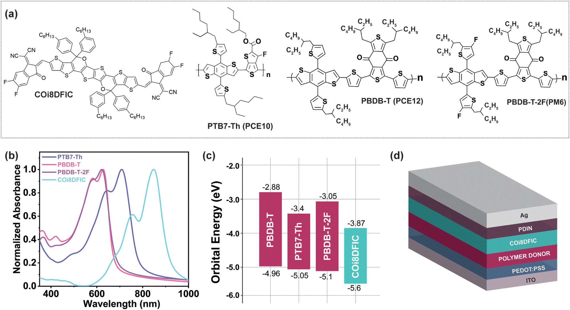 | ||
| Fig. 1 (a) The chemical structures of COi8DFIC, PTB7-Th, PBDB-T, and PBDB-T-2F, (b) normalized absorption spectra of pristine films of donor polymers and acceptor molecule, (c) orbital energy levels of the polymer donors (PTB7-Th, PBDB-T, and PBDB-T-2F) and non-fullerene acceptor (COi8DFIC) molecules (orbital energy level reference values were obtained from photoelectron spectroscopy data adapted from ref. 33), and (d) scheme of the device architecture of bilayer organic solar cells used for the study. | ||
Device optimization and photovoltaic characteristics
The current–voltage characteristic (J–V) of a typical polymer donor/COi8DFIC acceptor bilayer device with different acceptor layer thicknesses is shown in Fig. 2. Optimizing the acceptor layer thickness to approximately 40 nm distinctly improves device performance, as observed in the J–V characteristics of the b-OSCs. Table 1 summarizes the performance parameters of PTB7-Th/COi8DFIC (40 nm), PBDB-T/COi8DFIC (40 nm), and PBDB-T-2F/COi8DFIC (50 nm) b-OSCs with optimal acceptor layer thicknesses. The PTB7-Th/COi8DFIC b-OSCs exhibit the highest power conversion efficiency (PCE) of 11.42% for an acceptor layer thickness of about 40 nm, accompanied by a short-circuit current density (JSC) of 25.5 mA cm−2 and a fill factor (FF) of 66%. As the thickness of the COi8DFIC layer decreases to nearly 30 nm, the JSC drops significantly. Conversely, at a higher acceptor layer thickness of around 80 nm, both JSC and FF decrease from their optimum performance values. This response is consistent with insufficient acceptor layer thickness causing incomplete photon absorption, while a too-thick acceptor layer (double the optimal value) introduces significant charge carrier generation and transport losses due to incomplete exciton dissociation and non-geminate charge recombination.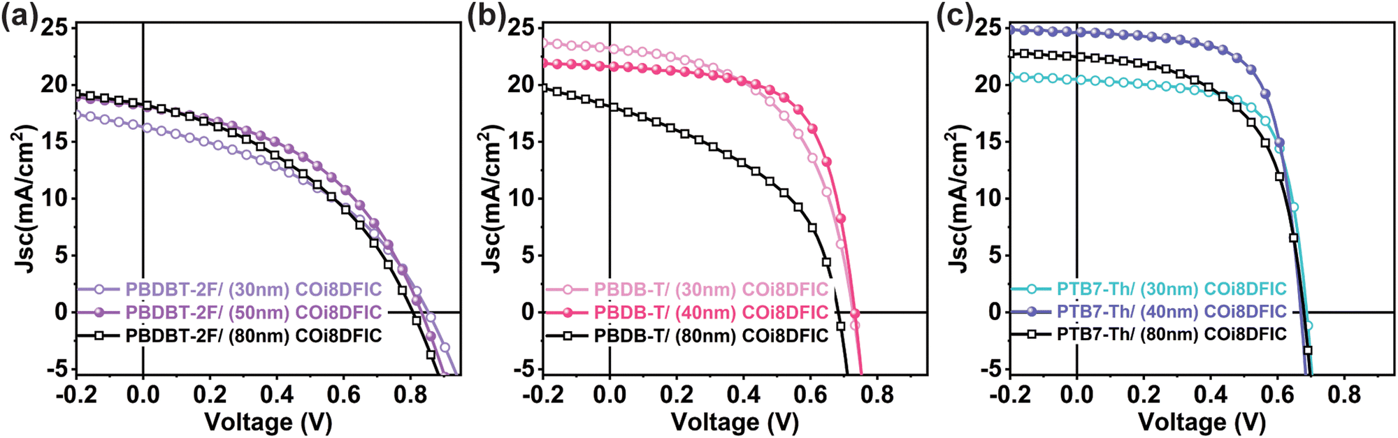 | ||
| Fig. 2 Typical J–V characteristics of bilayer organic solar cells under simulated AM1.5G (100 mW cm−2) illumination conditions with different acceptor layer thicknesses (a) PBDB-T-2F/COi8DFIC, (b) PBDB-T/COi8DFIC, and (c) PTB7-Th/COi8DFIC respectively. | ||
| Active layer | ΔIE (eV) | V OC(V) | J SC (mA cm−2) | FF (%) | PCE (%) |
|---|---|---|---|---|---|
| PBDB-T-2F/COi8DFIC | 0.50 | 0.835 ± 0.005 | 17.82 ± 0.33 | 44.11 ± 0.64 | 6.57 ± 0.15 |
| PTB7-Th/COi8DFIC | 0.55 | 0.679 ± 0.003 | 25.53 ± 0.74 | 65.91 ± 1.54 | 11.42 ± 0.45 |
| PBDB-T/COi8DFIC | 0.64 | 0.730 ± 0.005 | 22.17 ± 1.12 | 60.52 ± 4.59 | 9.78 ± 0.36 |
Similarly, in the case of PBDB-T/COi8DFIC, the highest PCE of ∼10% is obtained for an acceptor layer thickness of around 40 nm, with the PCE decreasing when the acceptor thickness deviates from this optimal value (Fig. S2, ESI†). A drop in FF is observed at a lower acceptor layer thickness of approximately 30 nm, accompanied by a marginal improvement in JSC. For the thick acceptor layer (about 80 nm), a reduction in both JSC and FF is observed, along with a notable loss in device open-circuit voltage (VOC). In addition to the free carrier recombination losses associated with a thick acceptor layer, the dissociation probability of excitons generated near the interface with the electron transport layer (PDIN) is relatively low, indicating an overall reduction in the J–V parameters.
A similar trend is observed in the PBDB-T-2F/COi8DFIC devices, with the highest PCE of 6.8% obtained for an intermediate acceptor layer thickness of around 50 nm. Changing the acceptor layer thickness to either 30 nm or 80 nm results in a notable reduction in JSC and FF, respectively. This set of observations indicates that an acceptor layer thickness of approximately 40 nm to 50 nm is necessary to extract the best performance parameters from a b-OSC using COi8DFIC as an acceptor. This optimal thickness is critical for enhancing photon harvesting and minimizing charge transport barriers, as variations in thickness primarily reflect a reduction in JSC or FF.
The enhanced JSC at an optimal COi8DFIC acceptor layer thickness (≈40–50 nm) is further confirmed by the external quantum efficiency (EQE) spectra measured under similar conditions (Fig. 3a and Fig. S3, ESI†). Notably, charge generation in the wavelength range associated with the acceptor molecule (λ ≈ 730–930 nm) is more pronounced in PTB7-Th/COi8DFIC-based OSCs compared to the other two combinations. This highlights efficient photon-to-charge conversion and reduced charge transport losses in PTB7-Th/COi8DFIC devices.35 These results suggest that an optimal IE offset of ≈0.55 eV ensures hole transfer from the COi8DFIC layer, provided minimal exciton loss occurs within the acceptor layer. However, PBDB-T/COi8DFIC devices also show improved charge generation due to an even higher IE offset (≈0.64 eV) as compared to PBDB-T-2F/COi8DFIC system, although carrier extraction barriers (obtained from transient photocurrent analysis, discussed later) significantly reduce the EQE within this wavelength range. These findings indicate that the simultaneous optimization of acceptor layer thickness and Frontier orbital energy offsets is critical for enhancing performance parameters.15,36
 | ||
| Fig. 3 (a) Typical external quantum efficiency (EQE) spectra of optimized PTB7-Th/COi8DFIC, PBDB-T/COi8DFIC, and PBDB-T-2F/COi8DFIC respectively, and (b) decay transient of picosecond-nanosecond transient absorption spectroscopy (ps-ns TAS) measurement on neat COi8DFIC film under dynamic vacuum (10−5 mbar). The fluence-dependent (1.1 μJ cm−2–16 μJ cm−2) singlet exciton decay (open symbols) fitted to the exciton–exciton annihilation model (solid lines) to estimate the diffusion length (≈39.4 nm) in COi8DFIC film. The exciton lifetime (τ) of the COi8DFIC was estimated using the TRPL spectroscopy decay at a low-excitation level (≈3 nJ cm−2), also superimposed in this figure (closed grey symbols). | ||
Estimation of exciton diffusion length
The significance of optimizing the acceptor layer thickness is studied through picosecond-nanosecond transient absorption spectroscopy (ps-ns TAS) and time-resolved photoluminescence spectroscopy (TRPL) measurements conducted on neat COi8DFIC films. The distance over which excitons can diffuse in organic materials is a critical factor influencing the performance of b-OSCs. A large exciton diffusion length in the acceptor and (or) donor material is a critical requirement for enhanced charge generation in b-OSCs.37,38We measured the exciton diffusion length LD in COi8DFIC film using the singlet–singlet annihilation (SSA) method.25,39,40 Details of exciton diffusion length calculation are provided in the ESI,† Section S5. In this approach, we analyzed fluence-dependent exciton decay in neat COi8DFIC films by fitting the decay to a global exciton annihilation model.25 The photo-induced absorption (PIA) decay kinetics of COi8DFIC films in the NIR region (∼1.1–1.2 eV) are presented in Fig. 3b. The ps–ns TA spectra are given in the ESI† (Fig. S4). The PIA decay kinetics show that the exciton decay accelerates substantially with increasing pump fluence (here from 1.1 μJ cm−2 to 16 μJ cm−2), indicating SSA. The singlet exciton lifetime τ is estimated as 250 ps by mono-exponential fit from TRPL measurements (Fig. 3b, grey symbols) with low excitation fluence (≈3 nJ cm−2) to ensure negligible exciton–exciton annihilation. The diffusion coefficient D was calculated using the expression, 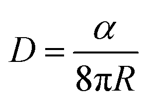 , where α is the singlet–singlet bimolecular exciton annihilation rate constant (1.55 × 10⁻⁷ cm3 s−1), and R is the molecular radius (≈1 nm), resulting in a diffusion coefficient of 0.061 cm2 s−1. According to the diffusion length equation
 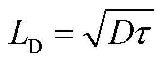 , the exciton diffusion length LD is estimated to be 39.4 nm.17,41,42
This implies that an acceptor layer thickness in the range of ≈40 nm is ideal for efficient photogeneration of charge carriers in b-OSCs based on COi8DFIC. Notably, the COi8DFIC acceptor exhibits one of the longest reported exciton diffusion lengths, thereby validating the rationale for its selection as a model NFA in this b-OSC optimization study.25,26,43
Charge carrier dynamics and the role of ionization energy offset
Even with the optimal COi8DFIC layer thickness ensuring maximal quenching of photogenerated excitons, the performance of each set of b-OSCs varies. An optimal IE offset for enhanced charge generation and minimal interfacial recombination in NFA-based OSCs is a critical requirement.6,32 In this study, the three distinct b-OSC systems employ different donor polymers (PBDB-T-2F, PTB7-Th, and PBDB-T), and they exhibit different IE offsets of 0.5 eV, 0.55 eV, and 0.64 eV, respectively, when combined with the NFA Coi8DFIC. The relationship between IE offset and charge generation in different NFA-based OSCs has been extensively investigated and was found to be a determining factor for efficient exciton dissociation in NFA-based systems.6,32,44–46 Notably, maintaining a moderate IE offset (∼0.5 to 0.6 eV), contrary to the requirement for a large electron affinity offset in fullerene-based OSCs, enhances charge generation efficiency, emphasizing the crucial role of donor polymer selection for a given NFA material.6 Furthermore, additional optimizations are necessary to facilitate efficient charge extraction, thereby achieving high JSC and FF from the device. We argue that the combination of optimal COi8DFIC layer thickness corresponding to its exciton diffusion length and an intermediate IE offset of about 0.55 eV is a crucial requirement for efficient charge generation and for suppressing charge carrier losses in COi8DFIC-based bilayer OSCs. A significant loss in JSC and FF is the main reason for the reduced PCE in devices employing the donors PBDB-T-2F and PBDB-T.To better understand the charge carrier extraction and recombination processes, transient photocurrent (TPC) and transient photovoltage (TPV) techniques were employed. In this technique, typically a sub-ns to microsecond wide light pulse excites the device photoactive layer, and the carrier generation is considered instantaneous.47,48 The resulting transient photocurrent decay profile in response to the light pulse provides information about the charge carrier extraction and recombination dynamics over various timescales.49,50 During the TPC measurement, the device is held at short-circuit condition, and the obtained TPC decay profile provides information on the distribution of carrier extraction times and charge carrier density. In TPV measurements, the device is kept at open-circuit condition to determine the carrier lifetimes.51,52
The transient photocurrent decay profile (Fig. 4a and b) reveals an effective carrier extraction time of τTPC = 690 ns in the PTB7-Th/COi8DFIC devices, along with an effective carrier lifetime of τTPV = 10.85 μs obtained from TPV measurements (Fig. 4c and Fig. S5, ESI†). In the case of PBDB-T-2F/COi8DFIC devices, even though there is a fast carrier extraction comparable to that of PTB7-Th-based devices, a short carrier lifetime indicates higher recombination losses.53 A similar trend of effective carrier extraction time vs. carrier lifetime is observed for the PBDB-T/COi8DFIC devices. Further, we examined the charge carrier dynamics in devices with varying COi8DFIC layer thicknesses (Fig. S6, ESI†). The TPC decay profiles demonstrate that carrier extraction becomes slower as the thickness of the acceptor film increases from 30 nm to 80 nm. In the optimal COi8DFIC thickness region, the carrier extraction becomes faster, indicating balanced carrier mobility and reduced charge transport resistance.54 This corroborates that the COi8DFIC thickness optimization close to its exciton diffusion length distinctly improves the device performance as observed in the J–V characteristics. However, we note that for the PBDB-T-2F/COi8DFIC system, the carrier extraction time observed for the thin acceptor layer (≈30 nm) is shorter than the optimal thickness. In the case of the best-performing PTB7-Th/COi8DFIC system, the carrier extraction times are τTPC = 0.81 μs, τTPC = 0.69 μs, and τTPC = 1.07 μs for COi8DFIC layer thickness of 30 nm, 50 nm, and 80 nm, respectively, indicating that an acceptor layer thickness equivalent to the exciton diffusion length is also advantageous for improved charge extraction. While at a higher active layer thickness, in addition to more transport resistance, an increased photon absorption in the acceptor region could lead to increased loss of excitons and free carrier to recombination.55,56 Additionally, the photogenerated excitons could not reach the D–A interface and can interact with separated charge carriers at the D–A interface, which further reduces the charge carrier extraction. This illustrates that when the acceptor film thickness exceeds the acceptor exciton diffusion length, more charge recombination occurs, resulting in less charge extraction and thus reduced device performance. This is evident from the TPC decay profiles of the PBDB-T/COi8DFIC system at different acceptor layer thicknesses.
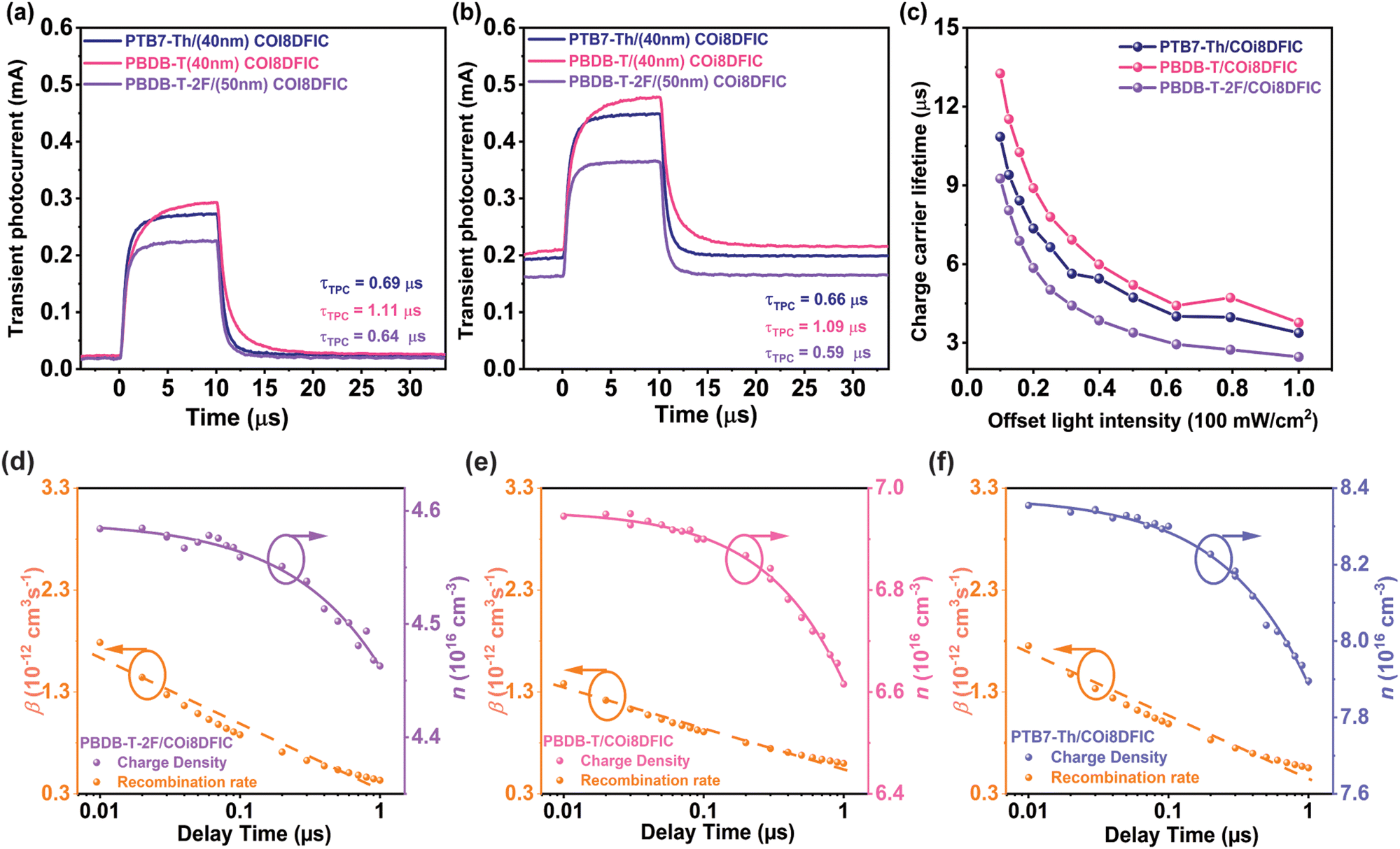 | ||
| Fig. 4 (a)–(c) Transient photocurrent profile of the PBDB-T-2F/COi8DFIC, PBDB-T/COi8DFIC, and PTB7-Th/COi8DFIC bilayer OSCs with optimal COi8DFIC thickness (a) background light intensity of ≈10 mW cm−2, (b) background light intensity of ≈79 mW cm−2, and (c) charge carrier lifetime obtained from transient photovoltage decay as a function of background light intensity (unit of 100 mWcm−2) for three combinations of optimized bilayer OSCs. (d)–(f) Bimolecular recombination coefficient and charge carrier density as a function of delay time (from 10 ns to 1 μs) obtained from Photo-CELIV traces to quantify charge extraction and recombination in optimized b-OSCs (d) PBDB-T-2F/COi8DFIC, (e) PBDB-T/COi8DFIC, (f) PTB7-Th/COi8DFIC (the solid lines are fit to the dispersive bimolecular recombination model and the dashed lines are guide for the eye). | ||
The extraction and recombination of free charge carriers were further examined by the time-delayed photo-charge extraction by linearly increasing voltage (photo-CELIV) technique.28,57,58 In this technique, the device is kept at open circuit condition for a delay time (tdel) after photoexcitation prior to charge extraction by a linearly increasing voltage. We carried out the photo-CELIV measurements on b-OSCs by varying the delay time from 10 ns to 1 μs after photoexcitation. In this way, we can gain insight into the bimolecular recombination processes in b-OSCs during the charge carrier transport and extraction processes.59 The photo-CELIV response of PTB7-Th/COi8DFIC, PBDB-T/COi8DFIC, and PBDB-T-2F/COi8DFIC devices follow a dispersive bimolecular recombination model as proposed in the literature.57 In this model, the bimolecular recombination is time-dependent due to the carrier relaxation towards tail states in the density of states.57,60 This results in a time-dependent charge carrier mobility and bimolecular recombination coefficient (β(t)).
Fig. 4d–f shows the charge carrier density and bimolecular recombination coefficient as a function of delay time in different optimized b-OSCs. The charge carrier density was obtained by integrating the current transients over the voltage ramp time. The key parameters from fitting to the dispersive bimolecular recombination model are summarized in Table 2. For the PTB7-Th/COi8DFIC device, a high initial charge carrier density (n0) of 8.38 × 1016 cm−3 and a bimolecular recombination coefficient β (at tdel = 10 ns) of 1.75 × 10⁻¹² cm−3 s−1 was obtained. Compared to the other two combinations, a high initial charge carrier density and, an intermediate bimolecular recombination coefficient suggest reduced bimolecular recombination and improved carrier extraction in PTB7-Th/COi8DFIC devices.49 It must be noted that PBDB-T/COi8DFIC b-OSCs also exhibit enhanced JSC and FF, but a slower carrier extraction (τTPC = 1.1 μs) compared to PTB7-Th/COi8DFIC (τTPC = 0.69 μs), suggesting an increased charge transport resistance.52,53 In the case of the PBDB-T-2F/COi8DFIC system, increased bimolecular recombination and trap-assisted recombination (γ = 0.69), along with low carrier density, introduce significant charge transport and extraction losses.
| Active layer | ΔIE (eV) | n 0 (1016 cm−3) | γ | τ b (10−5 s) | β (10−12 cm−3 s−1) |
|---|---|---|---|---|---|
| PTB7-Th/COi8DFIC | 0.55 | 8.38 | 0.75 | 4.07 | 1.75 |
| PBDB-T/COi8DFIC | 0.64 | 6.96 | 0.82 | 3.80 | 1.38 |
| PBDB-T-2F/COi8DFIC | 0.50 | 4.59 | 0.69 | 16.80 | 1.79 |
However, we anticipate that large ionization energy (IE) offset in the PBDB-T-2F/COi8DFIC system could lead to interfacial recombination, manifested as a reduced initial charge carrier density, which aligns with observations from external quantum efficiency (EQE) measurements. Nonetheless, systems with a high IE offset, such as PTB7-Th/COi8DFIC and PBDB-T/COi8DFIC, exhibit relatively higher initial charge carrier densities compared to systems with non-optimal IE offset (PBDB-T-2F/COi8DFIC). This highlights the critical role of efficient charge generation, which is equally important as charge extraction efficiency, as reflected in the EQE results. Additionally, we performed photo-CELIV measurements on various b-OSCs with different COi8DFIC layer thicknesses, as shown in Fig. S7–S10 (ESI†). They confirmed a significant bimolecular recombination loss in the PBDB-T-2F/COi8DFIC system, even when using a thin acceptor layer, indicating that additional carrier losses at the D–A interface and due to trap states occur.57 In contrast, an optimal IE offset (≈0.55 eV) in combination with fast carrier extraction and reduced bimolecular recombination enhances the device JSC and FF, resulting in the highest PCE for PTB7-Th/COi8DFIC b-OSCs.
Conclusion
In summary, we demonstrate the importance of simultaneous optimization of NFA layer thickness and the IE offset for efficient bilayer OSCs. The device optimization of bilayer OSCs using the highly crystalline NFA molecule COi8DFIC and the polymer donors PBDB-T-2F, PTB7-Th, and PBDB-T with increasing IE offsets (0.5 eV, 0.55 eV, and 0.64 eV) reveals a trend. The highest PCE is obtained in each donor–acceptor combination with an acceptor layer thickness of ∼40 nm, equivalent to the exciton diffusion length of the NFA COi8DFIC as estimated by transient absorption spectroscopy measurements. The critical requirement of optimal IE offset, in combination with the acceptor layer thickness tailored to match the exciton diffusion length, provides the highest PCE in the PTB7-Th/COi8DFIC devices possessing an IE offset of ∼0.55 eV. The optimal acceptor layer thickness and IE offset enabled enhanced charge generation by mitigating the exciton losses. Importantly, this optimization provides fast charge carrier extraction (≈690 ns) and moderate carrier lifetime (≈10.85 μs) in PTB7-Th/COi8DFIC devices, substantially improving the device short-circuit current and fill factor. High charge carrier density and comparably low bimolecular recombination losses determined from time-delayed photo-CELIV measurements corroborate these findings. This study highlights the importance of simultaneous optimization of NFA layer thickness, and IE offset as a design motif for reducing charge generation and recombination losses in bilayer OSCs.Experimental section
The architecture of b-OSCs is ITO/Donor polymer/COi8DFIC/PDIN/Ag. A thin layer (ca. 30 nm) of PEDOT:PSS (Clevios AL4083) was first spin-coated on the pre-cleaned ITO-coated glass substrates at 4000 rpm and baked at 150 °C for 15 min under ambient conditions. Subsequently, the donor and acceptor layers were prepared separately. The PTB7-Th (PBDB-T, PBDB-T-2F) solutions were prepared in CF at 8 mg mL−1 whereas COi8DFIC solutions were prepared in DCM at 10 mg mL−1. PDIN in carbinol with 0.3% acetic acid at 2 mg mL−1 was then spin-coated on the active layer at 4000 rpm. At the final stage, the substrates were pumped down in a high vacuum, and Ag (100 nm) was thermally evaporated onto the active layer.The current density–voltage (J–V) characteristics of b-OSCs were measured using a Keithley 2400 source meter in the glove box under AM 1.5G (100 mW cm−2) illumination conditions using a Enlitech solar simulator. The external quantum efficiency (EQE) spectra were measured using a Solar Cell Spectral Response Measurement System QE-R3011 (Enlitech Co., Ltd). The light intensity at each wavelength was calibrated using a standard monocrystalline Si photovoltaic cell. The transient photocurrent (TPC), transient photovoltage (TPV), and the Photo-CELIV measurements were conducted using the PAIOS electro-optical characterization module (Fluxim Co., Switzerland), integrated with the Setfos-Paios numerical simulation module. A global fitting approach was utilized to extract the device parameters.
TRPL measurements were performed on films spin-coated onto quartz substrates using the output of a Mode-locked Ti:Sa (Chameleon Ultra I from Coherent) fs laser operating at 80 MHz repetition rate, at 725![[thin space (1/6-em)]](https://www.rsc.org/images/entities/char_2009.gif) nm. An optical telescope (consisting of two plano-convex lenses) collected the PL of the samples, focused on the slit of a spectrograph (Princeton Instrument Spectra Pro SP2300), and detected with a Streak Camera (Hamamatsu C10910) system; a long pass filter (750 nm) was used. The excitation fluences used were between 0.3 to 3 nJ cm−2 where no fluence dependence was observed for these materials. The data were acquired in time-correlated single photon counting mode using the Streak Camera software (HPDTA) and exported to Origin 2021 for further analysis.
nm. An optical telescope (consisting of two plano-convex lenses) collected the PL of the samples, focused on the slit of a spectrograph (Princeton Instrument Spectra Pro SP2300), and detected with a Streak Camera (Hamamatsu C10910) system; a long pass filter (750 nm) was used. The excitation fluences used were between 0.3 to 3 nJ cm−2 where no fluence dependence was observed for these materials. The data were acquired in time-correlated single photon counting mode using the Streak Camera software (HPDTA) and exported to Origin 2021 for further analysis.
Transient absorption (TA) spectroscopy was carried out using a custom pump–probe setup. The output of a titanium:sapphire amplifier (Coherent LEGEND DUO, 4.5mJ, 3kHz, 100fs) was split into three beams (2, 1, and 1.5mJ). One of them was used to produce a white-light supercontinuum from 550 to 1700 nm by sending the 800 nm pulses through a sapphire (3 mm thick) crystal. The other two beams were used to pump two optical parametric amplifiers (OPA) separately (Light Conversion TOPAS Prime). TOPAS 1 generates tunable pump pulses, while TOPAS 2 generates signal (1300 nm) and idler (2000 nm) only. The pump–probe delay was adjusted by reducing the pump beam pathway between 5.12 and 2.6 m while the probe pathway length to the sample was kept constant at ≈5 m between the output of TOPAS 1 and the sample. The pump–probe path length was varied with a broadband retroreflector mounted on an automated mechanical delay stage (newport linear stage IMS600CCHA controlled by a Newport XPS motion controller), thereby generating delays between pump and probe from −400 ps to 8 ns. The samples (films on quartz substrates) were kept under vacuum (10−6mbar) during the measurements. The excitation wavelength used was 750nm. The transmitted fraction of the white light was guided to a custom-made prism spectrograph (Entwicklungsbüro Stresing), where it was dispersed by a prism onto a 512-pixel complementary metal–oxide–semiconductor (CMOS) linear image sensor (Hamamatsu G11608-512DA). The probe pulse repetition rate was 3kHz, while the excitation pulses were directly generated at 1.5kHz frequency, and the detector array was read out at 3kHz. Adjacent diode readings corresponding to the transmission of the sample after excitation and in the absence of an excitation pulse were used to calculate ΔT/T. Measurements were averaged over several thousand shots to obtain a good signal-to-noise ratio. The chirp induced by the transmissive optics was corrected with a custom MATLAB script. The delay at which the pump and probe arrive simultaneously on the sample (i.e., zero time) was determined from the point of the maximum positive slope of the TA signal rise for each wavelength.
Data availability
The data supporting this article have been included as part of the ESI.†Conflicts of interest
There are no conflicts to declare.Acknowledgements
S. K acknowledges financial support from the Scientific Research Startup funding (Grant No. QD2023005C), Shenzhen Science and Technology Program (JCYJ20240813112055071), and the National Natural Science Foundation of China (W2432044). Z. K. acknowledges the financial support from the National Natural Science Foundation of China (62275057) and the Guangxi Natural Science Foundation (2023GXNSFFA026004 and 2022GXNSFDA035066).References
- N. Jain, R. Jasiūnas, X. E. Li, H. Zhang, J. Fu, R. Zhang, L. Gang, M. Fahlman, V. Gulbinas and F. Gao, Adv. Energy Mater., 2024 DOI:10.1002/aenm.202403675.
- Y. Jiang, S. Sun, R. Xu, F. Liu, X. Miao, G. Ran, K. Liu, Y. Yi, W. Zhang and X. Zhu, Nat. Energy, 2024, 9, 975–986 CrossRef CAS.
- L. Zhu, M. Zhang, G. Zhou, Z. Wang, W. Zhong, J. Zhuang, Z. Zhou, X. Gao, L. Kan and B. Hao, Joule, 2024, 8(11), 3153–3168 CrossRef CAS.
- A. Armin, W. Li, O. J. Sandberg, Z. Xiao, L. Ding, J. Nelson, D. Neher, K. Vandewal, S. Shoaee and T. Wang, Adv. Energy Mater., 2021, 11, 2003570 CrossRef CAS.
- A. Azeez and K. Narayan, Energy Materials, World Scientific, 2023, pp. 1–33 Search PubMed.
- S. Karuthedath, J. Gorenflot, Y. Firdaus, N. Chaturvedi, C. S. De Castro, G. T. Harrison, J. I. Khan, A. Markina, A. H. Balawi and T. A. D. Peña, Nat. Mater., 2021, 20, 378–384 CrossRef CAS PubMed.
- G. Yu, J. Gao, J. C. Hummelen, F. Wudl and A. J. Heeger, Science, 1995, 270, 1789–1791 CrossRef CAS.
- Z. Han, K. Wang, Y. Chai, R. Zhang, J. Zhang, D. He, C. Wang and F. Zhao, J. Mater. Chem. C, 2024, 12, 3873–3880 RSC.
- Z. Chen, X. Chen, B. Qiu, G. Zhou, Z. Jia, W. Tao, Y. Li, Y. M. Yang and H. Zhu, J. Phys. Chem. Lett., 2020, 11, 3226–3233 CrossRef CAS PubMed.
- L. Ye, X. Jiao, S. Zhang, H. Yao, Y. Qin, H. Ade and J. Hou, Adv. Energy Mater., 2017, 7, 1601138 CrossRef.
- Y. Liu, J. Zhao, Z. Li, C. Mu, W. Ma, H. Hu, K. Jiang, H. Lin, H. Ade and H. Yan, Nat. Commun., 2014, 5, 5293 CrossRef CAS PubMed.
- B. Walker, A. B. Tamayo, X. D. Dang, P. Zalar, J. H. Seo, A. Garcia, M. Tantiwiwat and T. Q. Nguyen, Adv. Funct. Mater., 2009, 19, 3063–3069 CrossRef CAS.
- T. Yu and D. Ma, Solar RRL, 2024, 8, 2300751 CrossRef CAS.
- W. Köntges, P. Perkhun, J. Kammerer, R. Alkarsifi, U. Würfel, O. Margeat, C. Videlot-Ackermann, J.-J. Simon, R. R. Schröder and J. Ackermann, Energy Environ. Sci., 2020, 13, 1259–1268 RSC.
- A. Azeez and K. Narayan, J. Phys. Chem. C, 2021, 125, 12531–12540 CrossRef CAS.
- S. Karuthedath, Y. Firdaus, A. D. Scaccabarozzi, M. I. Nugraha, S. Alam, T. D. Anthopoulos and F. Laquai, Small Struct., 2022, 3, 2100199 CrossRef CAS.
- T. H. Lee, S. Y. Park, W.-W. Park, X. Du, J. H. Son, N. Li, O.-H. Kwon, H. Y. Woo, C. J. Brabec and J. Y. Kim, ACS Energy Lett., 2020, 5, 1628–1635 CrossRef CAS.
- T. Kumari, I. Vyalih, M. Á. L. Luna, H. Ahmed, M. Ahmad, R. Atajanov, E. Jayaraman, S. Manikandan, B. Paci and A. Di Carlo, Cell Rep. Phys. Sci., 2024, 5(6), 20 Search PubMed.
- M. H. Jee, H. S. Ryu, D. Lee, W. Lee and H. Y. Woo, Adv. Sci., 2022, 9, 2201876 CrossRef CAS PubMed.
- S. Y. Park, S. Chandrabose, M. B. Price, H. S. Ryu, T. H. Lee, Y. S. Shin, Z. Wu, W. Lee, K. Chen and S. Dai, Nano Energy, 2021, 84, 105924 CrossRef CAS.
- C. W. Tang, Appl. Phys. Lett., 1986, 48, 183–185 CrossRef CAS.
- L. Zhan, S. Li, X. Xia, Y. Li, X. Lu, L. Zuo, M. Shi and H. Chen, Adv. Mater., 2021, 33, 2007231 CrossRef CAS PubMed.
- Z. Zhao, S. Chung, Y. Y. Kim, M. Jeong, X. Li, J. Zhao, C. Zhu, S. Karuthedath, Y. Zhong and K. Cho, Energy Environ. Sci., 2024, 17, 5666–5678 RSC.
- A. Sanchez-Diaz, L. Burtone, M. Riede and E. Palomares, J. Phys. Chem. C, 2012, 116, 16384–16390 CrossRef CAS.
- Y. Firdaus, V. M. Le Corre, S. Karuthedath, W. Liu, A. Markina, W. Huang, S. Chattopadhyay, M. M. Nahid, M. I. Nugraha and Y. Lin, Nat. Commun., 2020, 11, 5220 CrossRef CAS PubMed.
- S. Chandrabose, K. Chen, A. J. Barker, J. J. Sutton, S. K. Prasad, J. Zhu, J. Zhou, K. C. Gordon, Z. Xie and X. Zhan, J. Am. Chem. Soc., 2019, 141, 6922–6929 CrossRef CAS PubMed.
- T. H. Lee, Y. Dong, R. A. Pacalaj, S. Y. Park, W. Xu, J. S. Kim and J. R. Durrant, Adv. Funct. Mater., 2022, 32, 2208001 CrossRef CAS.
- Y. Huang, S. Chung, S. Karuthedath, C. S. De Castro, H. Tang, M. Jeong, S. Lu, K. Cho, F. Laquai and Z. Kan, Solar RRL, 2023, 7, 2300267 CrossRef CAS.
- A. A. A. Torimtubun, M. J. Alonso-Navarro, A. Quesada-Ramírez, X. Rodríguez-Martínez, J. L. Segura, A. R. Goñi and M. Campoy-Quiles, Solar RRL, 2024, 8, 2400213 CrossRef CAS.
- Z. Zhao, J. Zhao, S. Chung, K. Cho, W. Xu and Z. Kan, ACS Mater. Lett., 2023, 5, 1718–1726 CrossRef CAS.
- W. Li, Z. Xiao, J. Cai, J. A. Smith, E. L. Spooner, R. C. Kilbride, O. S. Game, X. Meng, D. Li and H. Zhang, Nano Energy, 2019, 61, 318–326 CrossRef CAS.
- S. Karuthedath, S. H. Paleti, A. Sharma, H. Yin, C. S. P. De Castro, S. Chen, H. Xu, N. Alshehri, N. Ramos and J. I. Khan, Adv. Energy Mater., 2023, 13, 2203464 CrossRef CAS.
- J. Bertrandie, J. Han, C. S. De Castro, E. Yengel, J. Gorenflot, T. Anthopoulos, F. Laquai, A. Sharma and D. Baran, Adv. Mater., 2022, 34, 2202575 CrossRef CAS PubMed.
- H. Yin, C. Zhang, H. Hu, S. Karuthedath, Y. Gao, H. Tang, C. Yan, L. Cui, P. W. Fong and Z. Zhang, ACS Appl. Mater. Interfaces, 2019, 11, 48095–48102 CrossRef CAS PubMed.
- Q. Liao, Q. Kang, Y. Yang, Z. Zheng, J. Qin, B. Xu and J. Hou, CCS Chem., 2022, 4, 938–948 CrossRef CAS.
- J. B. Patel, P. Tiwana, N. Seidler, G. E. Morse, O. R. Lozman, M. B. Johnston and L. M. Herz, ACS Appl. Mater. Interfaces, 2019, 11, 21543–21551 CrossRef CAS PubMed.
- O. V. Mikhnenko, P. W. Blom and T.-Q. Nguyen, Energy Environ. Sci., 2015, 8, 1867–1888 RSC.
- S. M. Menke and R. J. Holmes, Energy Environ. Sci., 2014, 7, 499–512 RSC.
- J. D. Lin, O. V. Mikhnenko, J. Chen, Z. Masri, A. Ruseckas, A. Mikhailovsky, R. P. Raab, J. Liu, P. W. Blom and M. A. Loi, Mater. Horiz., 2014, 1, 280–285 RSC.
- G. J. Hedley, A. Ruseckas and I. D. Samuel, Chem. Rev., 2017, 117, 796–837 CrossRef CAS PubMed.
- M. T. Sajjad, A. Ruseckas and I. D. Samuel, Matter, 2020, 3, 341–354 CrossRef.
- B. Siegmund, M. T. Sajjad, J. Widmer, D. Ray, C. Koerner, M. Riede, K. Leo, I. D. W. Samuel and K. Vandewal, Adv. Mater., 2017, 29(12), 1604424 CrossRef PubMed.
- Z. Chen, S. Zhang, T. Zhang, J. Ren, J. Dai, H. Li, J. Qiao, X. Hao and J. Hou, Angew. Chem., 2024, 136, e202317892 CrossRef.
- J. Gorenflot, W. Alsufyani, M. Alqurashi, S. H. K. Paleti, D. Baran and F. Laquai, Adv. Mater. Interfaces, 2023, 10, 2202515 CrossRef CAS.
- A. Markina, K. H. Lin, W. Liu, C. Poelking, Y. Firdaus, D. R. Villalva, J. I. Khan, S. H. Paleti, G. T. Harrison and J. Gorenflot, Adv. Energy Mater., 2021, 11, 2102363 CrossRef CAS.
- M. Pranav, A. Shukla, D. Moser, J. Rumeney, W. Liu, R. Wang, B. Sun, S. Smeets, N. Tokmoldin, Y. Cao, G. He, T. Beitz, F. Jaiser, T. Hultzsch, S. Shoaee, W. Maes, L. Lüer, C. Brabec, K. Vandewal, D. Andrienko, S. Ludwigs and D. Neher, Energy Environ. Sci., 2024, 17, 6676–6697 RSC.
- C. Deibel and V. Dyakonov, Rep. Prog. Phys., 2010, 73, 096401 CrossRef.
- C. G. Shuttle, B. O’Regan, A. M. Ballantyne, J. Nelson, D. D. Bradley and J. R. Durrant, Phys. Rev. B: Condens. Matter Mater. Phys., 2008, 78, 113201 CrossRef.
- J. Wu, H. Cha, T. Du, Y. Dong, W. Xu, C. T. Lin and J. R. Durrant, Adv. Mater., 2022, 34, 2101833 CrossRef CAS PubMed.
- J. Vollbrecht, N. Tokmoldin, B. Sun, V. V. Brus, S. Shoaee and D. Neher, J. Appl. Phys., 2022, 131 Search PubMed.
- T. Zhu, L. Zheng, Z. Xiao, X. Meng, L. Liu, L. Ding and X. Gong, Solar Rrl, 2019, 3, 1900322 CrossRef CAS.
- E. Palomares, N. F. Montcada, M. Méndez, J. Jiménez-López, W. Yang and G. Boschloo, Characterization Techniques for Perovskite Solar Cell Materials, Elsevier, 2020, pp. 161–180 Search PubMed.
- M. Méndez, J. G. Sánchez, E. Martínez-Ferrero and E. J. Palomares, Curr. Opin. Colloid Interface Sci., 2024, 101865 CrossRef.
- Y. Firdaus, V. M. Le Corre, J. I. Khan, Z. Kan, F. Laquai, P. M. Beaujuge and T. D. Anthopoulos, Adv. Sci., 2019, 6, 1802028 CrossRef PubMed.
- A. Azeez and K. Narayan, Appl. Phys. Lett., 2020, 117(4), 3302 CrossRef.
- D. Neher, J. Kniepert, A. Elimelech and L. J. A. Koster, Sci. Rep., 2016, 6, 24861 CrossRef CAS PubMed.
- A. J. Mozer, G. Dennler, N. S. Sariciftci, M. Westerling, A. Pivrikas, R. Österbacka and G. Juška, Phys. Rev. B: Condens. Matter Mater. Phys., 2005, 72, 035217 CrossRef.
- A. J. Mozer, N. S. Sariciftci, L. Lutsen, D. Vanderzande, R. Österbacka, M. Westerling and G. Juška, Appl. Phys. Lett., 2005, 86(11), 2104 CrossRef.
- P. Mondelli, F. Silvestri, L. Ciammaruchi, E. Solano, E. Beltrán-Gracia, E. Barrena, M. Riede and G. Morse, J. Mater. Chem. A, 2021, 9, 26917–26928 RSC.
- G. Dennler, A. J. Mozer, G. Juška, A. Pivrikas, R. Österbacka, A. Fuchsbauer and N. S. Sariciftci, Org. Electron., 2006, 7, 229–234 CrossRef CAS.
Footnotes |
| † Electronic supplementary information (ESI) available. See DOI: https://doi.org/10.1039/d4tc05190d |
| ‡ Y. H. and A. A. contributed equally to this work. |
| § Present Address: Department of Chemistry, Ludwig-Maximilians-Universität München, Butenandtstraße 5-13 (E), D-81377 München, Germany. |
| This journal is © The Royal Society of Chemistry 2025 |