
 Open Access Article
 This Open Access Article is licensed under a Creative Commons Attribution-Non Commercial 3.0 Unported Licence
Enhancing the crystallinity and dielectric performance of ALD-grown SrTiO3 films by introducing a sub-nm-thick Pt layer†
Hong Keun
Chung‡
ab,
Jihoon
Jeon
ac,
Seungwan
Ye
ac,
Sung-Chul
Kim
 d,
Sung Ok
Won
d,
Tae Joo
Park
b and
Seong Keun
Kim
*ac
d,
Sung Ok
Won
d,
Tae Joo
Park
b and
Seong Keun
Kim
*ac
aElectronic Materials Research Center, Korea Institute of Science and Technology, Seoul 02792, Republic of Korea. E-mail: s.k.kim@kist.re.kr
bDepartment of Materials Science and Chemical Engineering, Hanyang University, Ansan 15588, Republic of Korea
cKU-KIST Graduate School of Converging Science and Technology, Korea University, Seoul 02841, Republic of Korea
dAdvanced Analysis and Data Center, Korea Institute of Science and Technology, Seoul 02792, Republic of Korea
First published on 20th February 2025
Abstract
SrTiO3 (STO), which has an exceptionally high dielectric constant, is a promising candidate for capacitor dielectrics for dynamic random-access memory (DRAM) applications. However, during atomic layer deposition (ALD), unwanted interfacial reactions with substrates, such as Ru, hinder its integration, which results in compositional nonuniformity and poor crystallinity. In this study, an ultrathin Pt layer (≤1 nm) is introduced as a reaction barrier, which effectively suppresses these interfacial reactions. This approach enabled the growth of high-quality stoichiometric STO films with enhanced crystallinity and dielectric performance. Despite its sub-nanometer thickness, the Pt layer notably improved the compositional uniformity and promoted film crystallization, which significantly increased the dielectric constants and reduced the equivalent oxide thickness (EOT). Post-deposition annealing (PDA) at 500 °C, compatible with DRAM fabrication, yielded an EOT of 0.34 nm with stable leakage currents and long-term reliability for STO films thinner than 10 nm. Furthermore, the area-selective growth characteristic of the ultrathin Pt layer eliminated the critical etching challenges of Pt, which facilitated selective growth on Ru and avoided unwanted growth on dielectric materials such as SiO2. This study presents a scalable, low-temperature solution for integrating STO into DRAM capacitors, thereby addressing critical fabrication challenges and advancing the potential of STO in memory applications.
1. Introduction
SrTiO3 (STO), with its perovskite crystal structure, has an extremely high dielectric constant of 300 at room temperature and a moderate bandgap of approximately 3.2 eV. These properties facilitate a much higher capacitance while maintaining a negligible charge loss under the application of an operating voltage. Consequently, STO has emerged as a promising capacitor dielectric in dynamic random-access memory (DRAMs),1–3 surpassing other high-k candidates including ZrO2,4,5 HfO2,6 and TiO2.7–11 The integration of STO in memory capacitors requires conformal film growth on complex structures with a high aspect ratio to achieve a high capacitance. Therefore, significant efforts have been dedicated to developing an atomic layer deposition (ALD) process for STO films,12–17 with the aim of achieving both high film quality and excellent conformality for such demanding structures.Despite the superior properties of STO, several challenges remain in the ALD of STO films for applications as capacitor dielectrics. These challenges include difficulties in crystallization, which requires annealing at temperatures beyond the thermal limits of DRAM fabrication.18 Furthermore, the issues commonly observed in STO ALD, such as compositional non-uniformity along the thickness direction and reduced capacitance caused by the presence of low-dielectric interfacial layers further hinders its practical application.19,20 These challenges in STO ALD primarily stem from the unwanted intense chemical reaction with the underlying substrate during the initial growth stage.19,20 This problem is particularly severe when Ru is used as the bottom electrode, a material increasingly favored for next-generation DRAM capacitors owing to its high work function and ease of etching compared to the other noble metals, which facilitates electrode patterning. As illustrated in Fig. 1(a), the initial overgrowth of SrOx on Ru substrates usually occurs in the initial stages of STO ALD, which induces compositional non-uniformity along the film thickness.19,21
 | ||
| Fig. 1 (a) Schematics of initial overgrowth of SrOx on Ru substrates during STO ALD. Such overgrowth induces the compositional non-uniformity along the film thickness. (b) A schematic illustrating a strategy to suppress interfacial reactions and enable the growth of high-quality STO films by introducing an ultrathin Pt layer. GIXRD patterns of (c) 16.4 nm-thick STO directly grown on Ru and (d) 12.8 nm-thick STO grown on 0.5 nm-thick Pt layer/Ru, in their as-grown state. (e) Bulk dielectric constant of STO films grown on Ru, 0.5 nm-thick Pt/Ru, and 1 nm-thick Pt/Ru after PDA at 500 °C. SEM images of 12.8 nm-thick STO grown on 0.5 nm-thick Pt/Ru (f) before and (g) after PDA at 500 °C. (h) Comparison of the dielectric performance demonstrates that the STO/ultrathin Pt/Ru capacitors.18,19,22,23 | ||
Two approaches have been proposed to prevent undesirable interactions with substrates. One involves the use of a less reactive Sr precursor to reduce the reactivity with the substrate.22 Although this approach alleviated interfacial reactions, it did not fundamentally resolve the issue.22 The other approach employed a reaction barrier layer between the STO and the substrate to prevent direct chemical interaction. Although the use of a dielectric layer, including Al2O324 or TiO2,25 as the reaction barrier layer effectively suppressed the interaction, the equivalent oxide thickness (EOT) of the capacitor significantly increased owing to the presence of a low-k dielectric layer.
In this study, an ultrathin Pt layer was introduced as a reaction barrier to fundamentally eliminate the interfacial reactions between STO and Ru electrodes. (Fig. 1(b)) Even though the ultrathin Pt layer was less than 1 nm thick, it successfully suppressed the reactions, which resulted in improved compositional uniformity and crystallization in the as-grown state. Consequently, this approach achieved high dielectric performance with post-deposition annealing (PDA) at a 500 °C, rendering it compatible for integration into DRAM fabrication processes. With the continued scaling of DRAM capacitors, the space available for thin films becomes increasingly constrained. Therefore, the use of a sub-nanometer-thick layer to eliminate interfacial reactions offers a significant advantage in addressing these spatial limitations. Moreover, employing an ultrathin Pt layer resolves the challenge of etching Pt owing to its area-selective deposition capability.
2. Results and discussion
Most studies on STO ALD have reported that STO films are typically amorphous in the as-grown state, and require high-temperature PDA above 600 °C for crystallization.18,22,26 However, the introduction of an ultrathin Pt layer markedly affects the crystallinity of the films, even in the as-grown state. An ultrathin Pt layer was grown on Ru through ALD, followed by the ALD of the STO films on top (Fig. 1(b)). Fig. 1(c) and (d) show the grazing incident X-ray diffraction (GIXRD) patterns of (c) 16.4 nm-thick STO directly grown on Ru and (d) 12.8 nm-thick STO grown on 0.5 nm-thick Pt layer/Ru. The 16.4 nm-thick STO film grown directly on Ru exhibited no XRD peaks, which indicates that the film was amorphous and is consistent with the findings of other literature on amorphous formation.27,28 In contrast, the STO film grown on 0.5 nm-thick Pt/Ru exhibited an STO (110) Bragg peak, even with a thickness of 12.8 nm. This indicates that the introduction of an ultrathin Pt layer facilitated the crystallization of the STO films, even in the as-grown state. This difference in the crystallinity of STO can also be verified by the change in the dielectric constants. Fig. 1(e) shows the bulk dielectric constant of STO films grown on Ru, 0.5 nm-thick Pt/Ru, and 1 nm-thick Pt/Ru after PDA at 500 °C. STO grown directly on Ru had a low dielectric constant of approximately 25, whereas STO with an ultrathin Pt layer exhibited a significantly higher dielectric constant of approximately 143, which is comparable to that of crystalline STO.18,22 Despite identical deposition and annealing conditions, this substantial difference in the dielectric constant highlights the critical role of the ultrathin Pt layer in enhancing the crystallinity of STO films.The quality of the films, including their densities, significantly improved as well. Previous studies have reported the formation of cracks in STO films after PDA owing to densification,22 which is indicative of low film quality. However, as shown in Fig. 1(f) and (g), and Fig. S1 in the ESI,† only a slight increase in surface roughness was detected after PDA, with no evidence of cracks. This further confirmed that superior quality of the STO films was achieved with the introduction of an ultrathin Pt layer.
Consequently, the dielectric performance of the capacitors with STO films was significantly improved by the use of an ultrathin Pt layer. As shown in Fig. 1(h), comparison of the dielectric performances demonstrates that the STO/ultrathin Pt/Ru capacitors achieved a very low EOT value of 0.34 nm at a leakage current limit (10−7 A cm−2) under an operation voltage of 0.8 V. This was achieved within a maximum processing temperature of 500 °C. Fig. 1(h) also includes a comparison with other STO studies, which exhibited higher EOT values despite employing high processing temperatures exceeding 600 °C, which is incompatible with the DRAM fabrication process.18,19,22,23
To function effectively as a reaction barrier, the ultrathin Pt layer should fully coat the Ru electrode, even at sub-nanometer thicknesses. The ALD growth of noble metals, such as Pt, usually forms islands rather than a continuous layer in the initial growth stage,29–32 which can result in incomplete coverage. However, in this study, the ALD of Pt exhibited a negligible nucleation delay on Ru (Fig. S2, ESI†), which suggests the feasibility of achieving full coverage. To verify this, a model-based analysis was employed using angle-resolved X-ray photoelectron spectroscopy (ARXPS) to estimate the Pt coverage on the Ru electrode. The illustration in Fig. 2(a) shows that the coverage of the Pt layer and the intensity ratio of the Pt and Ru peaks in the XPS analysis are correlated. Using ARXPS, a quantitative model was developed to determine the thickness and coverage of the Pt layer on Ru (Note S3, ESI†).
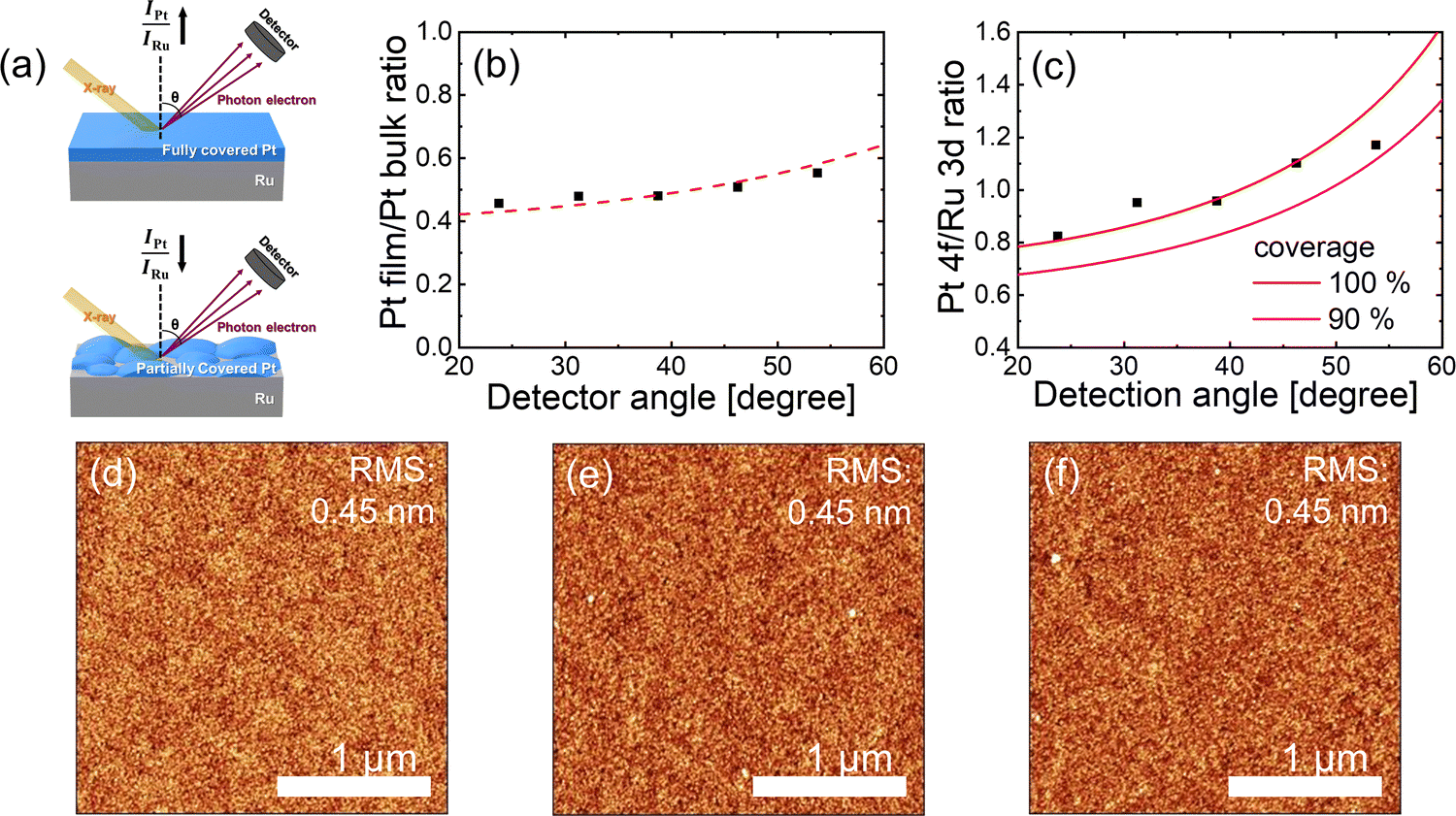 | ||
| Fig. 2 (a) A schematic illustrating coverage analysis of ultrathin Pt layer on Ru by comparing the intensity ratio of Pt and Ru peaks in the ARXPS analysis. Variations in (b) the Pt film/Pt bulk XPS intensity ratio of the 0.5 nm-thick Pt layer on Ru and (c) the intensity ratio of Pt 4f and Ru 3d peaks of the layer in terms of the emission angle. AFM images of the (d) Ru, (e) 0.5 nm-thick Pt/Ru, and (f) 1 nm-thick Pt/Ru thin films, respectively. | ||
Fig. 2(b) and (c) show the variations in (b) the Pt film/Pt bulk intensity ratio of the Pt layer on Ru and (c) the intensity ratio of the Pt 4f and Ru 3d peaks in terms of the emission angle. The thickness of the Pt grown on Ru, estimated to be 0.5 nm from wavelength dispersive X-ray fluorescence (WDXRF), served as a reference for corroborating the ARXPS quantitative model. The Pt thickness determined from ARXPS was 0.58 nm, which is consistent with the WDXRF measurement. The coverage determined by fitting the Pt 4f/Ru 3d intensity ratio was estimated to be close to 100%, even for such a thin Pt layer. Fig. 2(d)–(f) show the atomic force microscopy (AFM) images of the (d) Ru, (e) 0.5 nm-thick Pt/Ru, and (f) 1 nm-thick Pt/Ru thin films. No islands were observed after Pt ALD. The surface roughness (root-mean-squared roughness values: 0.45 nm for all samples) remained almost unchanged irrespective of the Pt growth. This indicates that Pt grew in a layer-by-layer mode rather than in an island growth mode on the Ru substrate. Noble metals in ALD typically form islands because of their high surface energies. However, the surface energy (3075 mJ m−2)33 of Ru was slightly higher than that (2601 mJ m−2)33 of Pt. This difference in surface energy is believed to facilitate full coverage of Ru by Pt, even at sub-nanometer thicknesses.
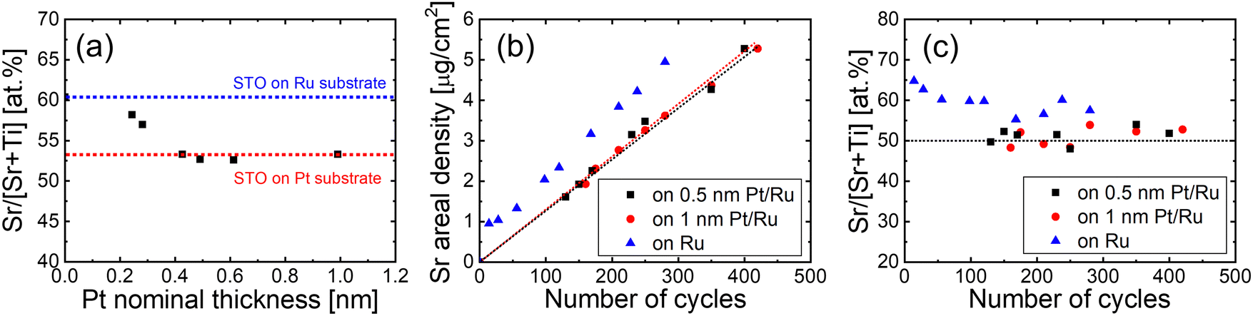
To evaluate the effectiveness of the fully covered Pt layer as a reaction barrier and to determine the minimum required thickness, STO films were grown on Ru substrates with varying Pt thicknesses. Fig. 3(a) shows the variation in the Sr/[Sr + Ti] atomic ratio of the STO films as a function of the thickness of the Pt reaction barrier layer. All STO films were grown under identical conditions optimized for stoichiometric composition on a sufficiently thick Pt layer. An STO film directly grown on Ru exhibited an Sr/[Sr + Ti] ratio of 60%, which indicates an Sr-rich composition. As the Pt thickness increased, the Sr/[Sr + Ti] ratio decreased to 52% above a Pt thickness of 0.4 nm. The minimum thickness is comparable to the lattice constant (0.3905 nm) of the Pt unit cell. This suggests that a Pt layer of only one unit cell in thickness effectively acts as a reaction barrier, and prevents undesired reactions between the STO film and the Ru substrate.
 | ||
| Fig. 3 (a) Variation in the Sr[Sr + Ti] atomic ratio of the STO films as a function of the thickness of the Pt reaction barrier layer. Variations in (b) the areal density of Sr ions and (c) the Sr/[Sr + Ti] atomic ratio in the STO films as a function of the number of ALD cycles. | ||
As the Pt thickness increased, the SrOx deposits in the films decreased, whereas the TiOx deposits remained unchanged. (Fig. S4, ESI†) Therefore, the composition change induced by the introduction of the ultrathin Pt layer is attributed to the suppression of initial excess growth of SrOx. Fig. 3(b) shows the variation in the areal density of the Sr ions in the STO films as a function of the number of ALD cycles. The growth per cycle, obtained from the slope of the graph remained similar, irrespective of the presence of the Pt layer. However, the y-intercept, which represents the initial excess growth of SrOx, differed depending on the presence of the Pt layer. The introduction of 0.5 nm and 1 nm-thick Pt layers rendered the y-intercept negligible, which enabled the films to achieve a stoichiometric composition across all thicknesses (Fig. 3(c)).
Fig. 4(a) and (b) show the GIXRD patterns of STO films with thicknesses of 5.6 nm and 12.8 nm, grown on 0.5 nm-thick Pt/Ru substrates, in their (a) as-grown state and (b) after PDA at 500 °C. The 5.6 nm-thick STO showed no Bragg peaks in the as-grown state. However, the thicker 12.8 nm-thick film exhibited a clear (110) STO peak, even without PDA, thereby demonstrating improved crystallinity. Achieving a uniform composition across the film thickness is critical for improving the crystallinity of STO films grown on ultrathin Pt/Ru.
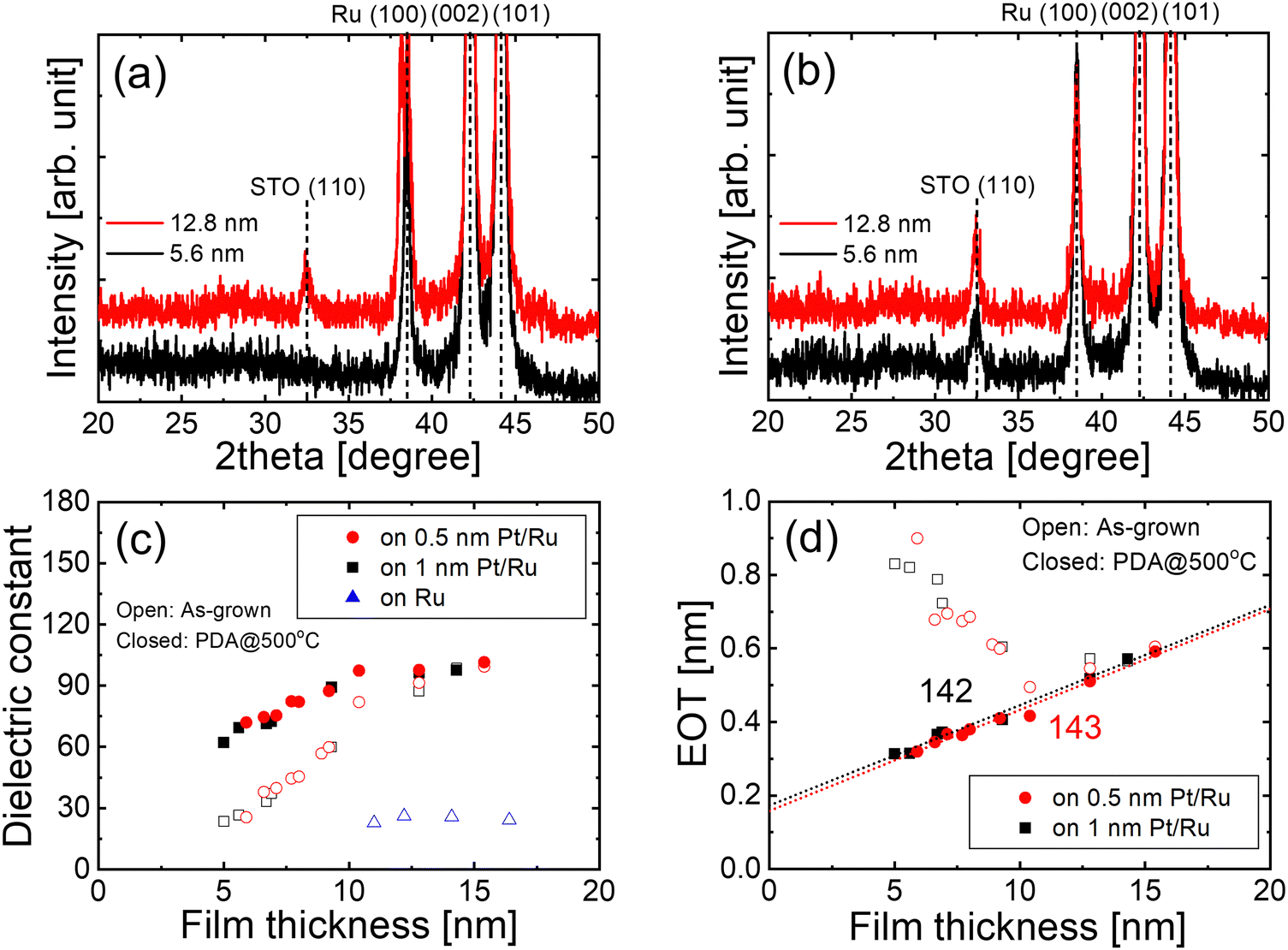 | ||
| Fig. 4 GIXRD patterns of STO films with thicknesses of 5.6 nm and 12.8 nm, grown on 0.5 nm-thick Pt/Ru substrates, in their (a) as-grown state and (b) after PDA at 500 °C. (c) Variation in the dielectric constant of STO films grown on Ru, 0.5 nm- and 1 nm-thick Pt/Ru before and after PDA at 500 °C. (d) Variation in the EOT of STO films grown on 0.5 nm- and 1 nm-thick Pt/Ru before and after PDA at 500 °C. | ||
Because crystallinity strongly influences the dielectric constant, the dielectric constant was analyzed as a function of film thickness. As shown in Fig. 4(c), the STO films grown directly on Ru exhibited a low dielectric constant of approximately 25 even with thicknesses up to 17 nm. This indicates that the films remained amorphous, which is consistent with the XRD result in Fig. 1(c). In contrast, STO films grown on 0.5 nm- and 1 nm-thick Pt/Ru substrates exhibited a significant increase in the dielectric constant with increasing thickness, from ∼30 at 5 nm to ∼100 at 12.5 nm in the as-grown state. This indicates an enhanced crystallinity with increasing film thickness. Fig. 4(d) shows the variation in the EOT values of the as-grown STO films as a function of the film thickness. Interestingly, the EOT value decreased as the thickness increased to approximately 10 nm, further supporting the idea that crystallinity improved with increasing film thickness. Thickness-dependent crystallization was previously reported in stoichiometric STO films grown by ALD, where the crystallinity improved as thickness increased.34 The consistency with the previous report supports that the introduction of the ultrathin Pt layer plays a critical role in forming high-quality, stoichiometric STO films.
Full crystallization was not achieved in the as-grown state for films thinner than 10 nm. Therefore, PDA was performed at a low temperature of 500 °C, which is compatible with DRAM fabrication. The 5.6 nm-thick film was crystallized upon PDA (Fig. 4(b)). After PDA, the dielectric constant of the films, especially for the thinner films, significantly improved (Fig. 4(c)). However, a slight decrease in the dielectric constant with decreasing film thickness was still observed even after PDA. This phenomenon results from the low-k interfacial layer caused by intrinsic dead layer effects rather than partial crystallization. As shown in Fig. 4(d), the EOT of the annealed STO films grown on ultrathin Pt/Ru was linearly proportional to the film thickness. This linear relationship suggests that the bulk dielectric constant, excluding the effects of the interfacial layer, remained constant with the thickness. This implies that full crystallization occurred after PDA, because the bulk dielectric constants were similar across all thicknesses. The estimated bulk dielectric constants were almost identical for films grown on 0.5- and 1 nm-thick Pt/Ru (Fig. 1(e) and Fig. 4(d)). This indicates that even with 0.5 nm-thick Pt layer, the STO films were fully crystallized and achieved high dielectric constants.
Fig. 5(a) and (b) show the leakage current density – applied voltage curves of the STO films grown on (a) 0.5 nm- and (b) 1 nm-thick Pt/Ru, respectively. PDA at 500 °C improved leakage properties. Most of the previous studies on STO have achieved stable leakage properties for films thicker than 10 nm. However, STO films grown on ultrathin Pt/Ru demonstrated excellent leakage properties, even below 10 nm. The improvement in the leakage current is attributed not only to the formation of high-quality STO films but also to the increase in the energy barrier at the STO/electrode interface. While Ru exhibits a work function of approximately 4.8 eV, the introduction of a 0.5 nm-thick Pt layer increased the work function to 5.0 eV. (Fig. S6, ESI†) It has been reported that covering metal electrodes with an upper layer possessing a higher work function could increase their work function35 and this increased energy barrier likely contributes to the further suppression of leakage currents. Although slight differences in the thickness of the STO films made precise comparisons of the leakage currents between different Pt thicknesses challenging, no significant differences in the leakage properties were observed. Fig. 5(c) shows the time-dependent dielectric breakdown (TDDB) of the 6.6 nm-thick STO film grown on 1 nm-thick Pt/Ru as a function of the applied voltage. The STO film achieved an EOT of 0.34 nm with a leakage current density of 2.3 × 10⁻⁷ A cm−2 at 0.8 V. The extrapolated operating voltage for a 10-year lifetime was determined to be 0.83 V, which exceeds the expected operating voltage for next-generation DRAM capacitors.
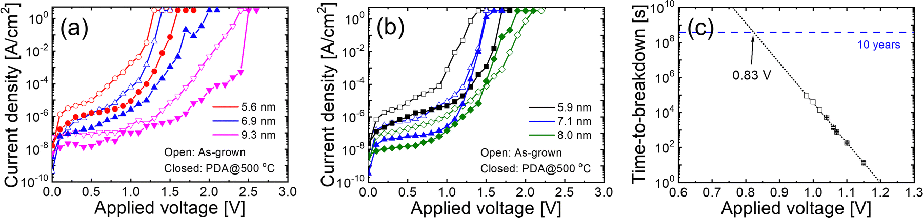 | ||
| Fig. 5 Leakage current density – applied voltage curves of the STO films grown on (a) 0.5 nm- and (b) 1 nm-thick Pt/Ru. (c) TDDB of the 6.6 nm-thick STO film grown on 1 nm-thick Pt/Ru as a function of the applied voltage. | ||
A significant concern associated with Pt electrodes is the difficulty of etching Pt, which limits its commercial use. The proposed STO/ultrathin Pt/Ru structure illustrated in Fig. 6(a) fundamentally resolves this issue. The ALD process for a Pt layer typically exhibits area-selective deposition characteristics, where Pt preferentially grows on metallic surfaces such as Ru and not on low-surface-energy dielectrics such as SiO2.30 This area-selective deposition hinders the formation of a Pt layer on the dielectrics as a nongrowth area, thereby eliminating the need for etching. Furthermore, the ultrathin Pt layer proposed in this study enhanced the efficiency of selective growth, which enabled well-defined Pt patterns without an additional etching process. Fig. 6(b)–(e) display the (b) scanning electron microscopy (SEM) image and Auger electron spectroscopy (AES) elemental maps of (c) Pt, (d) Ru, and (e) Si for a 0.5 nm-thick Pt grown on a patterned Ru/SiO2 substrate. Pt was selectively deposited on the patterned Ru surfaces, with no deposition on SiO2. This observation highlights the exceptional selectivity of ALD and supports the feasibility of using ultrathin Pt layers in electrode applications for high-quality STO films, without adding complexity to the etching steps.
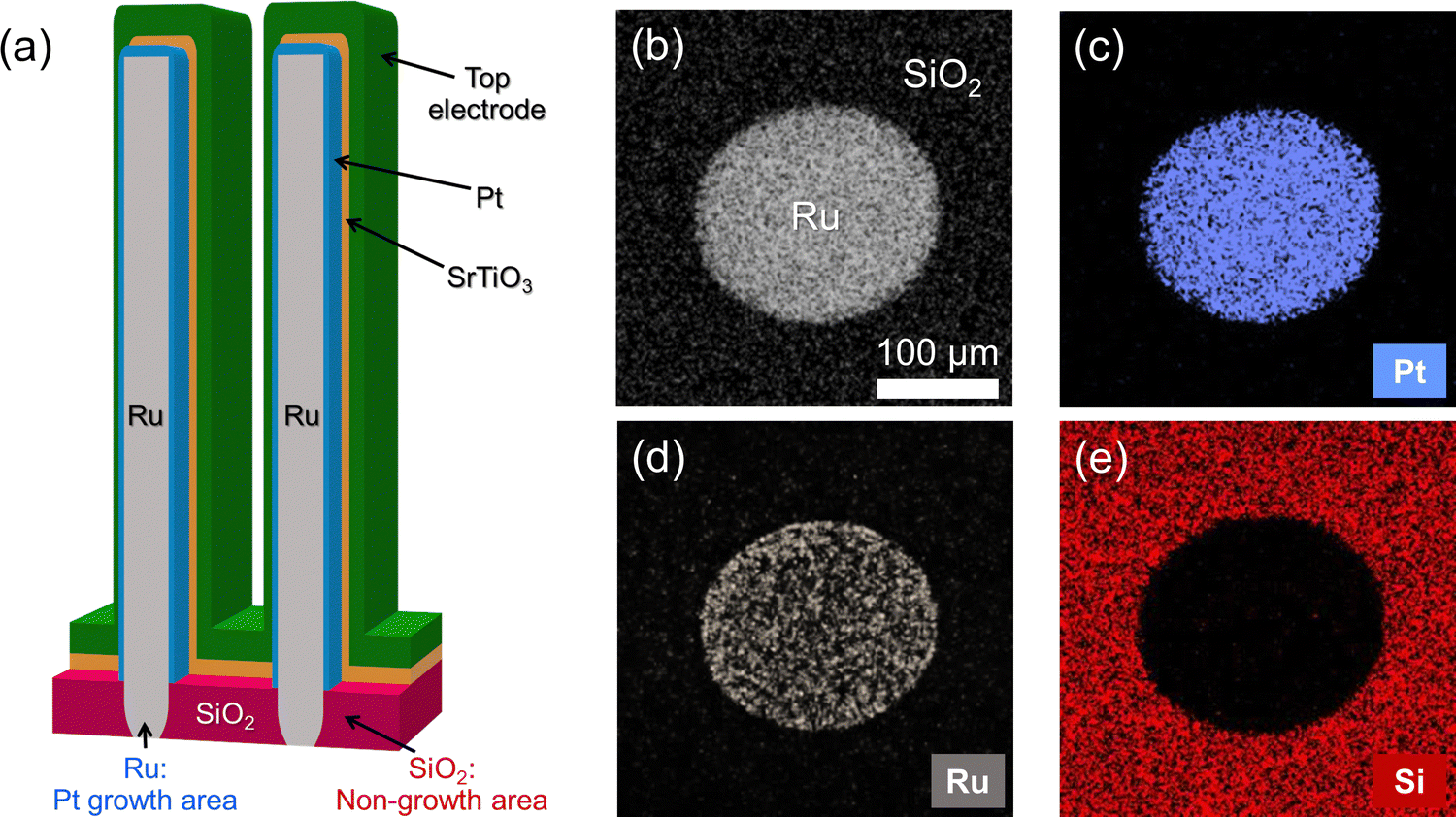 | ||
| Fig. 6 (a) Schematic of the proposed STO/ultrathin Pt/Ru structure, eliminating the need for Pt etching through the area-selective growth characteristics of the ultrathin Pt layer. (b) SEM image and AES elemental maps of (c) Pt, (d) Ru, and (e) Si for an 0.5 nm-thick Pt grown on a patterned Ru/SiO2 substrate. | ||
3. Conclusion
In this study, a novel strategy to address the challenges associated with ALD of STO for memory capacitors is demonstrated by introducing an ultrathin Pt layer. Even at sub-nanometer thicknesses, this layer effectively suppressed undesirable interfacial reactions with the Ru electrodes, which facilitated the growth of high-quality stoichiometric STO films. This approach improved the compositional uniformity and enhanced the crystallinity of the films, which significantly increased in their dielectric constant and reduced EOT. After PDA at 500 °C, which is compatible with the DRAM fabrication process, the STO/ultrathin Pt/Ru capacitors achieved an EOT as low as 0.34 nm with stable leakage properties and long-term reliability, even for films thinner than 10 nm. These improvements are attributed not only to the high-quality STO films, but also to the increased energy barrier at the STO/electrode interface owing to the higher work function of the Pt layer.Moreover, the challenging etching ability, a critical issue associated with Pt electrodes was also addressed. The ALD of ultrathin Pt exhibits area-selective deposition characteristics, which enables precise growth on Ru surfaces without growth on dielectrics such as SiO2. This eliminated the need for complex etching steps and significantly enhanced the practical applicability of ultrathin Pt layers in capacitor fabrication. The combination of high dielectric performance, compatibility with low-temperature processes, and etching-free integration makes the STO/ultrathin Pt/Ru structure a promising candidate for next-generation DRAM capacitors. This study highlights the potential of ultrathin Pt layers to revolutionize the application of STO films in DRAM technologies by addressing critical fabrication challenges, while satisfying stringent performance requirements.
4. Experimental
4.1. Film growth
STO films were grown in a custom-built chamber by ALD at 380 °C. Sr(iPr3Cp)2 and Ti(CpMe5)(OMe)3 (SK Trichem Co.) were used as Sr and Ti sources, respectively. The bottles containing the precursors were heated to 80 °C for Sr(iPr3Cp)2 and 90 °C for Ti(CpMe5)(OMe)3. The precursor molecules were delivered to the chamber at an Ar carrier-gas flow rate of 200 sccm. The STO films were grown by alternating the sub-cycles of SrO and TiO2, with the sub-cycle ratio varied to achieve a stoichiometric value. H2O vapor was used as the oxygen source for SrO growth, whereas O3 was used for the growth of TiO2. The dose of H2O vapor was controlled by chilling the canister containing H2O at 15 °C, and O3 with a high concentration of 180 g Nm−3 was produced using an inductive type O3 generator. Sputtered Ru(30 nm)/TaOx(5 nm)/SiO2/Si coupons were used as the substrates. Ultrathin Pt layers were grown on the Ru substrate through ALD at 250 °C using MeCpPtMe3 and O2 before the growth of the STO films. Some STO films were annealed at 500 °C in an O2 atmosphere for 30 min to achieve full crystallization.4.2. Characterization
The areal density of each cation in the films was determined by WDXRF (ZSZ Primus II, Rigaku). The cation composition and film thickness were estimated from areal densities. An ARXPS (Theta Probe, Thermo Fisher Scientific) with an areal detector was used for parallel acquisition measurements to determine the thickness and coverage of the Pt layer on Ru. The crystallinity of the films was examined using GIXRD at an incidence angle of 1°. The surface morphologies of the films were observed using SEM (Inspect F, FEI) and AFM (MFP-3D-SA, Asylum Research).4.3. Device fabrication
Metal-insulator-metal capacitors were fabricated to evaluate their dielectric properties. Circular RuO2 top electrodes with a radius of 100 μm were formed through a lift-off process after patterning with a photolithography process. Capacitance was measured using an Agilent 4294A impedance analyzer at 10 kHz. Leakage properties were determined using an Agilent 4155A semiconductor parameter analyzer. Electrical measurements were performed at room temperature.Author contributions
The manuscript was written through contributions of all authors. All authors have given approval to the final version of the manuscript.Data availability
The data that support the findings of this study are available upon request from the corresponding author upon reasonable request.Conflicts of interest
There are no conflicts to declare.Acknowledgements
This research was supported by the R&D Convergence Program (CAP22033-000) of the National Research Council of Science and Technology of Korea, the MOTIE (1415187483), KSRC (RS-2023-00234833) support program for the development of the future semiconductor device, and the KIST institutional program (2V10330-24-P043).References
- S. K. Kim and M. Popovici, MRS Bull., 2018, 43, 334–339 CrossRef.
- S. K. Kim, S. W. Lee, J. H. Han, B. Lee, S. Han and C. S. Hwang, Adv. Funct. Mater., 2010, 20, 2989–3003 CrossRef CAS.
- S. E. Kim, J. Y. Sung, J. D. Jeon, S. Y. Jang, H. M. Lee, S. M. Moon, J. G. Kang, H. J. Lim, H.-S. Jung and S. W. Lee, Adv. Mater. Technol., 2023, 8, 2200878 CrossRef CAS.
- M. Pešić, S. Knebel, M. Geyer, S. Schmelzer, U. Böttger, N. Kolomiiets, V. V. Afanas'ev, K. Cho, C. Jung, J. Chang, H. Lim, T. Mikolajick and U. Schroeder, J. Appl. Phys., 2016, 119, 064101 CrossRef.
- M. Jang, J. Jeon, W. C. Lim, K. H. Chae, S.-H. Baek and S. K. Kim, Ceram. Int., 2024, 50, 47910–47915 CrossRef CAS.
- J. Kim, B. S. Kim, A. J. Lee, D. H. Han, J. H. Hwang, Y. Kim, K.-C. Song, H. Oh, S. Kim, Y. Park and W. Jeon, Ceram. Int., 2022, 48, 3236–3242 CrossRef CAS.
- S. K. Kim, W. D. Kim, K. M. Kim, C. S. Hwang and J. Jeong, Appl. Phys. Lett., 2004, 85, 4112–4114 CrossRef CAS.
- S. K. Kim, G. J. Choi, S. Y. Lee, M. Seo, S. W. Lee, J. H. Han, H. S. Ahn, S. Han and C. S. Hwang, Adv. Mater., 2008, 20, 1429–1435 CrossRef CAS.
- T. Kim, J. Jeon, S. H. Ryu, H. K. Chung, M. Jang, S. Lee, Y. J. Chung and S. K. Kim, ACS Appl. Mater. Interfaces, 2024, 16, 33877–33884 CrossRef CAS PubMed.
- J. Jeon, T. Kim, M. Jang, H. K. Chung, S.-C. Kim, S. O. Won, Y. Park, B. J. Choi, Y. J. Chung and S. K. Kim, Chem. Mater., 2024, 36, 3326–3333 CrossRef CAS.
- H. K. Chung, S. O. Won, Y. Park, J.-S. Kim, T. J. Park and S. K. Kim, Appl. Surf. Sci., 2021, 550, 149381 CrossRef CAS.
- S. W. Lee, J. H. Han, O. S. Kwon and C. S. Hwang, J. Electrochem. Soc., 2008, 155, G253 CrossRef CAS.
- M. Popovici, K. Tomida, J. Swerts, P. Favia, A. Delabie, H. Bender, C. Adelmann, H. Tielens, B. Brijs, B. Kaczer, M. A. Pawlak, M.-S. Kim, L. Altimime, S. Van Elshocht and J. A. Kittl, Phys. Status Solidi A, 2011, 208, 1920–1924 CrossRef CAS.
- S. H. Kim, W. Lee, C. H. An, Y. Kim, D. S. Kwon, D.-G. Kim, S. H. Cha, S. T. Cho, J. Lim and C. S. Hwang, Phys. Status Solidi RRL, 2019, 13, 1900373 CrossRef CAS.
- N. Menou, X. P. Wang, B. Kaczer, W. Polspoel, M. Popovici, K. Opsomer, M. A. Pawlak, W. Knaepen, C. Detavernier, T. Blomberg, D. Pierreux, J. Swerts, J. W. Maes, P. Favia, H. Bender, B. Brijs, W. Vandervorst, S. V. Elshocht, D. J. Wouters, S. Biesemans and J. A. Kittl, 2008 IEEE International Electron Devices Meeting, 2008 DOI:10.1109/IEDM.2008.4796852.
- M. Popovici, A. Belmonte, H. Oh, G. Potoms, J. Meersschaut, O. Richard, H. Hody, S. V. Elshocht, R. Delhougne, L. Goux and G. S. Kar, 2018 IEEE International Electron Devices Meeting (IEDM), 2018 DOI:10.1109/IEDM.2018.8614673.
- B.-E. Park, J. Lee, J. Bang, E. Do, E. Kim, C. An, S. Y. Park, S. Lee, D.-J. Yun, J. Lee, Y. Kim and H.-J. Kim, ACS Appl. Mater. Interfaces, 2024, 16, 49957–49965 CrossRef CAS PubMed.
- W. Lee, S. Yoo, W. Jeon, Y. W. Yoo, C. H. An, M. J. Chung, H. J. Kim, S. W. Lee and C. S. Hwang, Thin Solid Films, 2015, 589, 723–729 CrossRef CAS.
- S. W. Lee, J. H. Han, S. Han, W. Lee, J. H. Jang, M. Seo, S. K. Kim, C. Dussarrat, J. Gatineau, Y.-S. Min and C. S. Hwang, Chem. Mater., 2011, 23, 2227–2236 CrossRef CAS.
- W. Lee, J. H. Han, W. Jeon, Y. W. Yoo, S. W. Lee, S. K. Kim, C. H. Ko, C. Lansalot-Matras and C. S. Hwang, Chem. Mater., 2013, 25, 953–961 CrossRef CAS.
- S. H. Kim, W. Lee, C. H. An, D.-G. Kim, D. S. Kwon, S. T. Cho, S. H. Cha, J. I. Lim and C. S. Hwang, Phys. Status Solidi RRL, 2019, 13, 1800557 CrossRef.
- W. Lee, W. Jeon, C. H. An, M. J. Chung, H. J. Kim, T. Eom, S. M. George, B. K. Park, J. H. Han, C. G. Kim, T.-M. Chung, S. W. Lee and C. S. Hwang, Chem. Mater., 2015, 27, 3881–3891 CrossRef CAS.
- M. A. Pawlak, B. Kaczer, W. C. Wang, M. S. Kim, M. Popovici, J. Swerts, K. Tomida, K. Opsomer, M. Schaekers, C. Vrancken, B. Govoreanu, A. Belmonte, C. Demeurisse, I. Debusschere, L. Altimime, V. V. Afanas’ev and J. A. Kittl, 2011 Symposium on VLSI Technology - Digest of Technical Papers, 2011 Search PubMed.
- W. Lee, J. H. Han, S. W. Lee, S. Han, W. J. Jeon and C. S. Hwang, J. Mater. Chem., 2012, 22, 15037–15044 RSC.
- M. A. Pawlak, J. Swerts, M. Popovici, B. Kaczer, M.-S. Kim, W.-C. Wang, K. Tomida, B. Govoreanu, J. Delmotte, V. V. Afanas’ev, M. Schaekers, W. Vandervorst and J. A. Kittl, Appl. Phys. Lett., 2012, 101, 042901 CrossRef.
- S. W. Lee, O. S. Kwon, J. H. Han and C. S. Hwang, Appl. Phys. Lett., 2008, 92, 222903 CrossRef.
- M. A. Pawlak, B. Kaczer, M.-S. Kim, M. Popovici, K. Tomida, J. Swerts, K. Opsomer, W. Polspoel, P. Favia, C. Vrancken, C. Demeurisse, W.-C. Wang, V. V. Afanas’ev, W. Vandervorst, H. Bender, I. Debusschere, L. Altimime and J. A. Kittl, Appl. Phys. Lett., 2010, 97, 162906 CrossRef.
- N. Aslam, V. Longo, W. Keuning, F. Roozeboom, W. M. M. Kessels, R. Waser and S. Hoffmann-Eifert, Phys. Status Solidi A, 2014, 211, 389–396 CrossRef CAS.
- V. Vandalon, A. J. M. Mackus and W. M. M. Kessels, J. Phys. Chem. C, 2022, 126, 2463–2474 CrossRef CAS PubMed.
- J. J. Pyeon, C. J. Cho, S.-H. Baek, C.-Y. Kang, J.-S. Kim, D. S. Jeong and S. K. Kim, Nanotechnology, 2015, 26, 304003 CrossRef PubMed.
- H. K. Chung, H. Kim, J. Jeon, S.-C. Kim, S. O. Won, R. Harada, T. Tsugawa, Y. J. Chung, S.-H. Baek, T. J. Park and S. K. Kim, J. Phys. Chem. Lett., 2023, 14, 6486–6493 CrossRef CAS PubMed.
- H. Kim, T. Kim, H. K. Chung, J. Jeon, S.-C. Kim, S. O. Won, R. Harada, T. Tsugawa, S. Kim and S. K. Kim, Small, 2024, 20, 2402543 CrossRef CAS PubMed.
- F. Aqra and A. Ayyad, Appl. Surf. Sci., 2011, 257, 6372–6379 CrossRef CAS.
- H. K. Chung, J. Jeon, H. Kim, M. Jang, S.-C. Kim, S. O. Won, I.-H. Baek, Y. J. Chung, J. H. Han, S. H. Cho, T. J. Park and S. K. Kim, Appl. Surf. Sci., 2024, 664, 160243 CrossRef CAS.
- S. K. Kim, S. Han, W. Jeon, J. H. Yoon, J. H. Han, W. Lee and C. S. Hwang, ACS Appl. Mater. Interfaces, 2012, 4, 4726–4730 CrossRef CAS PubMed.
Footnotes |
| † Electronic supplementary information (ESI) available: The following files are available free of charge. SEM images, growth per cycle of Pt on Ru, modelling based on ARXPS, area densities of Sr and Ti ions in the films in terms of Pt thickness, capacitance – applied voltage, ultraviolet photoelectron spectroscopy (PDF). See DOI: https://doi.org/10.1039/d4tc05377j |
| ‡ Current address: Samsung Electronics. |
| This journal is © The Royal Society of Chemistry 2025 |