
 Open Access Article
 This Open Access Article is licensed under a
 Creative Commons Attribution 3.0 Unported Licence
Low-temperature atomic layer deposition of metastable MnTe films for phase change memory devices†
Gwangsik Jeon a,
Jeongwoo Jeona,
Woohyun Kima,
Daehyeon Kimb,
Wontae Nohb,
Wonho Choia,
Byongwoo Parka,
Sangmin Jeona,
Sungjin Kima,
Chanyoung Yoo*c and
Cheol Seong Hwang*a
a,
Jeongwoo Jeona,
Woohyun Kima,
Daehyeon Kimb,
Wontae Nohb,
Wonho Choia,
Byongwoo Parka,
Sangmin Jeona,
Sungjin Kima,
Chanyoung Yoo*c and
Cheol Seong Hwang*a
aDepartment of Materials Science and Engineering, and Inter-University Semiconductor Research Center, Seoul National University, Seoul, 08826, Republic of Korea. E-mail: cheolsh@snu.ac.kr
bAir Liquide Korea Co., Ltd, Seoul, 03722, Republic of Korea
cDepartment of Materials Science and Engineering, Hongik University, Seoul, 04066, Republic of Korea. E-mail: cyyoo0117@snu.ac.kr
First published on 10th February 2025
Abstract
This work demonstrates an atomic layer deposition (ALD) process for achieving the MnTe film with metastable β phase at a growth temperature of 100 °C. By employing a nitrogen-coordinated Mn precursor (bis[bis(trimethylsilyl)amido]manganese(II)) and co-injecting NH3 with the Te precursor (bis(trimethylsilyl)telluride(II)), stoichiometric and high-purity β-MnTe films were deposited with self-limiting behavior on SiO2 substrate at a growth temperature of 100 °C. The metastable β phase was stabilized without needing non-equilibrium synthesis methods, offering smooth (root-mean-squared roughness ∼0.55 nm) nanocrystalline films with excellent uniformity and conformality on both planar and high-aspect-ratio structures. Substrate- and temperature-dependent growth behaviors revealed that the formation of β-MnTe is governed by the chemical bonding environment, with the phase transitioning to the stable α phase on conductive substrates or at higher growth temperatures. Annealing studies demonstrated the β to α phase transition via a displacive transformation, highlighting the feasibility of the ALD MnTe films for future phase change memory devices. This work offers insights into the ALD of metastable-phase chalcogenides, enabling their integration into advanced electronic devices.
Introduction
Transition metal chalcogenides are known to have unique electrical, optical, and magnetic properties and have received considerable interest in various fields.1,2 MnTe, one of the transition metal chalcogenides, is a polymorphic semiconductor that can exist in different phases depending on the temperature.3 The α phase, the most stable structure at room temperature, is a p-type semiconductor with an octahedrally coordinated NiAs-type nickeline structure (NC) and a bandgap of 1.37–1.51 eV.4 The β phase is a metastable structure below 949 °C, with a tetrahedrally coordinated wurtzite structure (WZ). It is also a p-type semiconductor with a wider bandgap of 2.5–2.7 eV, exhibiting significant electrical and optical contrasts with the α phase.5 Recent studies have shown that β-MnTe films undergo polymorphic transformation to α-MnTe while maintaining crystallographic orientation through displacive transformation,6 and the structural changes between NC and WZ structures can be reversibly controlled.7 Unlike conventional phase change memory (PCM) materials, which require melting followed by rapid quenching for amorphization, the crystalline-to-crystalline transition in β-MnTe does not involve melt-quenching and occurs through a diffusionless mechanism. This mechanism offers advantages such as faster switching speeds and lower energy consumption, as it minimizes entropic losses associated with atomic movement. The unique characteristic of not involving an amorphous phase makes β-MnTe a promising candidate for next-generation PCM devices.However, stabilizing the metastable β phase without high pressure or non-equilibrium synthesis methods remains challenging, limiting its practical application. Several groups have attempted to solve this issue by adopting low-temperature deposition methods. For example, sputtering on amorphous InZnO substrates,8 ZnTe seed layers,9 or alloying with ZnTe10 or MnSe11 were introduced. However, these approaches presented limitations for practical applications, as they rely on specific template-assisted methods or result in impure MnTe films. Meanwhile, room-temperature sputtering of MnTe films was reported for the β-MnTe film deposition.7 Nonetheless, physical deposition techniques still have limitations in achieving conformal coverage over complex structures, which is essential for advanced device applications like vertical-type PCM devices.12 Therefore, an advanced deposition technique capable of stabilizing metastable β-MnTe films with high conformality is required to apply β-MnTe to advanced memory devices.
Atomic layer deposition (ALD) is a preferred deposition technique with its self-limiting deposition characteristics, which allow precise thickness control and uniform deposition of high-quality films on complex structures. Also, ALD can achieve the desired film stoichiometry through an appropriate selection of precursors.13,14 Hence, extensive research has been performed on precursor chemistry and ALD process technology for various chalcogenide thin films.12,15 However, ALD of transition metal tellurides presents fundamental challenges, particularly in achieving sufficient reactivity of Te sources at low temperatures compared to commonly used oxygen sources (H2O, O2, and O3) or sulfur sources (H2S). This limitation complicates the desired chemical reaction for film deposition, especially when depositing metastable phases, such as β-MnTe, that can transform into stable counterparts (α-MnTe) upon receiving sufficient thermal energy during high-temperature processing, which may be necessary to achieve sufficient chemical reactivity of the Te sources. While plasma-enhanced ALD (PEALD) is often used to enhance reactivity at low deposition temperatures,14,16 it exhibits disadvantages such as plasma-induced damage, limited step coverage, and increased complexity of the deposition system.17
Another problem with depositing thin films containing highly oxidizing transition metals, such as Mn, is the contamination from unwanted chemical species during deposition. For example, MnTe films quickly oxidize at temperatures as low as 130 °C even under high vacuum conditions (∼0.01 Torr),18 showing the extreme vulnerability of MnTe to oxidation. Also, unlike sputtering processes using high-purity targets, ALD processes could involve contamination from by-products generated during chemical reactions of the precursors. This issue becomes more severe at low deposition temperatures, where probable physical condensation of the by-products increases impurity incorporation.19 Consequently, activating the Te source, suppressing the oxidation, and minimizing the contamination by carefully optimizing process variables, such as the choice of precursors and the injecting sequence, become critical for feasibly depositing high-quality MnTe films in metastable phases at low temperatures.
This study introduces an ALD process for the β-MnTe film through two key strategies at low temperatures. First, a nitrogen-coordinated Mn precursor was selected to ensure high reactivity while minimizing film contamination. Second, the NH3 gas was co-injected with the Te precursor to facilitate chemical reactions at low temperatures by generating reactive H2Te and modifying surface groups to highly reactive –NH2 surface groups. This combined approach enabled stoichiometric and metastable β-MnTe film deposition at temperatures as low as 100 °C, with uniform nucleation and growth and excellent conformality over three-dimensional hole structure. Despite the low deposition temperature, the resulting β-MnTe films were highly crystalline and free of impurities. The origin of the transition of the deposited phase was further supported by systematic studies of substrate- and temperature-dependent growth behaviors, providing insights into the underlying deposition and specific phase formation mechanism. The deposited β-MnTe films demonstrated potential for PCM applications through annealing tests, suggesting that this process design strategy offers valuable insights into the ALD of other metastable-phase transition metal tellurides.
Experimental
MnTe films were deposited using an ALD reactor with a 12-inch-diameter showerhead and an 8-inch-wafer-compatible substrate heater (CN-1, Plus-200). Bis[bis(trimethylsilyl)amido]manganese(II) (BTMSA-Mn, Mn(N(SiMe3)2)2, Air Liquide, Inc.) and bis(trimethylsilyl)telluride(II) (BTMS-Te, Te(SiMe3)2, Soulbrain, Inc.) were used as Mn and Te precursors, respectively. The Mn and Te precursors were kept in stainless steel canisters and heated to 78 and 30 °C, respectively, to maintain a vapor pressure of 1 torr for both. Films were grown on dry oxidized 100-nm-thick SiO2/Si, sputtered 50-nm-thick TiN/SiO2/Si, or glass substrates.The Mn precursors were carried to the ALD chamber by the bubbling method with Ar carrier gas at a flow rate of 50 standard cubic centimeters per min (sccm), and the Te precursors were carried by the vapor draw method with the same Ar flow rate. 50 sccm of NH3 was co-injected with the Te precursor through a separate gas line. For the purge process, 200 sccm of Ar gas was used. The working pressure of the process chamber was maintained within the 1 ± 0.5 torr range during the deposition.
X-ray fluorescence spectroscopy (XRF, Thermo Scientific, Qunt’X EDXRF) measured the film's layer density (LD) and composition. The crystallinity and bulk density of the films were measured using glancing angle X-ray diffraction (GAXRD) and X-ray reflectivity (XRR) using an X-ray diffractometer (PANalytical, X’Pert PRO MPD). Scanning electron microscopy (SEM, Hitachi, S-4800) and atomic force microscopy (AFM, NX10, Park systems) were used to measure the surface morphology of the deposited films. Spectroscopic ellipsometry (SE, M-2000, J. A. Woollam) was used to determine the optical properties of deposited films.
Density functional theory (DFT) computations were conducted using Gaussian09W software. The energies and geometries of the relevant molecules were calculated utilizing Becke's three-parameter hybrid functional in conjunction with the Lee, Yang, and Parr correlation functional, denoted as B3LYP. The 6-31G(d) basis set was employed for H, C, N, and Si, while the LanL2DZ basis set was utilized for Mn, Te. All reactions were simulated at 1 Torr and 100 °C in the gas phase to replicate the experimental conditions.
Depth profile analysis by Auger electron spectroscopy (AES, ULVAC-PHI, PHI-700) confirmed the impurity concentration. Rutherford backscattering spectrometry (RBS, National Electrostatics CORP, 6SDH-2) confirmed the layer density and composition of the deposited films. X-ray photoelectron spectroscopy (XPS, PHI, Versaprobe 3) was performed to verify the chemical bonding states of the elements. The XPS peaks were calibrated with reference to the binding energy of the C 1s peak at 284.8 eV from the adventitious carbon, measured before Ar+ ion sputtering. Cross-sectional transmission electron microscopy (TEM) and energy dispersive spectroscopy (EDS) were used to investigate the microstructure and composition of the film onto a nanoscale deep hole structure by using double spherical aberration-corrected TEM (Cs-TEM, JEM-ARM200F, JEOL). TEM specimens were prepared with a focused ion beam (Helios G4, Thermo Fisher Scientific).
The temperature dependence of the resistance of the MnTe film was investigated using the two-point probe method. In this measurement, a 100 nm-thick W layer was patterned to prepare the contact electrodes by a shadow mask to measure the resistance change behavior of the MnTe film. The distance between the two contact electrodes was 985 μm. The remaining MnTe surface was covered with an ∼5 nm Al2O3 layer to prevent severe oxidation.
Results and discussion
Precursor selection and process design for low-temperature ALD of MnTe
Fig. 1a shows the chemical structures of the two precursors used for MnTe ALD. The Mn precursor was carefully selected to deposit MnTe at low temperatures, considering various factors. Table S1 (ESI†) summarizes the characteristics of Mn precursors commonly used in the ALD of Mn-containing films. The predominantly used and commercially available Mn precursors for ALD are carbon-coordinated ones. Bulky cyclopentadienyl ligands form weak bonds with the metal center via π-electron donation, which enhances reactivity and stabilizes the metal complex. However, these precursors have limited reactivity toward the Te precursor and low thermal stability, which can result in unwanted carbon incorporation.20,21 On the other hand, oxygen-coordinated Mn precursors have been widely studied for depositing manganese-based oxides.22–25 For example, the tris(2,2,6,6-tetramethyl-3,5-heptanedionato)manganese(III), (Mn(thd)3) precursor enabled the deposition of the high-purity manganese oxides at high process temperatures with an activated oxygen source.22 However, when attempting the growth of tellurides, the oxygen ions included in the Mn(thd)3 could result in the unwanted oxidation of the deposited film. Therefore, nitrogen-coordinated Mn precursors were recently proposed to solve these issues, offering high reactivity and volatility at low temperatures, and high thermal stability.26 Still, no ALD application for MnTe film growth has yet been demonstrated. | ||
| Fig. 1 (a) Chemical structures of the Mn and Te precursors. (b) ALD sequence for the deposition of MnTe. (c) Process scheme of the ALD reaction mechanism of MnTe ALD through NH3 co-injection. (d)–(g) ALD saturation behavior through the Mn and Te precursors' injection/purge time split (100 °C). | ||
The divalent Mn precursor, BTMSA-Mn, which contains two bulky trimethylsilylamine (TMSA) ligands, was selected for MnTe ALD for depositing a 1![[thin space (1/6-em)]](https://www.rsc.org/images/entities/char_2009.gif) :1 stoichiometric film with the divalent Te precursor (BTMS-Te). The TMSA ligands stabilize the +2 oxidation state of Mn, while the relatively weak Mn-ligand and strong N–Si bonds promote efficient ligand exchange reactions.27 The identical TMSA ligands have also been adopted in Ge precursors for GeTe and GeSe ALDs, which have shown excellent ligand exchange reactivity with chalcogenide precursors even at low temperatures.28,29 This suggests a high likelihood that BTMSA-Mn would also enable low-temperature deposition, suitable for depositing a metastable β phase. Additionally, BTMSA-Mn has a sufficiently high vapor pressure, which is advantageous for highly conformal deposition on complex structures.
:1 stoichiometric film with the divalent Te precursor (BTMS-Te). The TMSA ligands stabilize the +2 oxidation state of Mn, while the relatively weak Mn-ligand and strong N–Si bonds promote efficient ligand exchange reactions.27 The identical TMSA ligands have also been adopted in Ge precursors for GeTe and GeSe ALDs, which have shown excellent ligand exchange reactivity with chalcogenide precursors even at low temperatures.28,29 This suggests a high likelihood that BTMSA-Mn would also enable low-temperature deposition, suitable for depositing a metastable β phase. Additionally, BTMSA-Mn has a sufficiently high vapor pressure, which is advantageous for highly conformal deposition on complex structures.
Initial ALD attempts using only the Mn and Te precursor (Mn precursor/Ar purge/Te precursor/Ar purge) resulted in no film growth. Similar issues have been reported for other telluride (GeTe and Sb2Te3) film growth, which were resolved by co-injecting NH3 with the BTMS-Te.30,31 Based on the findings, an ALD process utilizing NH3 co-injection with the Te precursor was designed to facilitate sequential ALD reactions in MnTe ALD (Fig. 1b). During the process, NH3 serves two critical functions (Fig. 1c). First, NH3 reacts with the Te precursor to generate reactive H2Te intermediate precursors in the gas phase (i). Also, NH3 converts the bulky N(SiMe3)2 groups into more reactive NH2 groups on the growing film surface (ii). Finally, these modified surface groups readily react with H2Te to form Mn–Te bonds, enabling the facile growth of the MnTe film (iii). DFT calculations validated this reaction pathway's likelihood (Table S2, ESI†), which revealed negative enthalpy and Gibbs free energy changes for forming reactive intermediates and subsequent film growth, indicating spontaneous reactions. These theoretical calculations support that NH3 co-injection effectively facilitates the ALD reactions at low temperatures by generating reactive intermediates and modifying surface groups to enhance reactivity. Fig. S1 in the ESI† describes the effects of various NH3 injection methods on film composition and growth in detail.
The precursor injection pulse and purge pulse times were varied to study the saturation growth behavior. Fig. 1d–g demonstrates the self-limiting characteristics of the ALD chemical reaction by showing the growth per cycle (GPC) as a function of Mn and Te precursor injection and purge times at a growth temperature of 100 °C on SiO2 and TiN substrates. GPC was calculated by dividing the LD (measured by XRF) by the number of cycles (100 cycles). The closed and open symbols correspond to films grown on SiO2 and TiN substrates, respectively. The black symbols represent the growth per cycle (left y-axis), while the blue symbols indicate the x value in the MnxTe1−x composition (right y-axis). The GPC was saturated with sufficient precursor injection and Ar purge times, confirming the typical self-limiting nature of the ALD process. Additionally, the consistent 1:1 Mn to Te composition indicates that the +2 and −2 oxidation states of the Mn and Te precursors were well retained despite the co-injection of NH3. As a result, the optimized injection and purge times were determined to be 4 seconds for Mn injection, 20 seconds for the following Ar purge, 2 seconds for Te + NH3 co-injection, and 30 seconds for the following Ar purge.
Characterization of MnTe films: phase formation and growth behavior on different substrates and temperatures
The characteristics of the MnTe ALD process and deposited films at a temperature of 100 °C were analyzed, revealing substrate-dependent behavior. Fig. 2a shows the LD increase as a function of the cycle number for the films grown on SiO2 and TiN substrates. The films on both substrates maintained a 1:1 composition as the number of cycles increased with linear growth behaviors. However, the GPC, determined from the slopes of the best-linear-fitted graphs, differs significantly: 34.3 ng cm−2 cyc for SiO2 and 66.0 ng cm−2 cyc for TiN. A higher GPC was observed on TiN compared to SiO2, which suggests potential differences in growth behavior. Along with these growth variations, GAXRD analysis revealed distinctly different crystalline phases on each substrate (Fig. 2b). A diffraction peak at 24.32° on SiO2 substrate corresponds to the metastable β-phase MnTe (002) plane, consistent with MnTe films sputtered at room temperature under high vacuum.7 This finding indicates that the designed ALD conditions allowed stabilization of the metastable β phase by keeping the thermal energy below the threshold for α phase formation while enabling a facile reaction between Mn and Te precursors. Meanwhile, on TiN substrate, a stable α phase was formed, as indicated by several peaks at 26.49°, 28.26°, 36.67°, 43.84°, and 47.86° (JCPDS 01-086-1022).
 | ||
| Fig. 2 Analysis of 100 °C grown MnTe films. (a) Layer density and composition over the ALD cycles. (b) GAXRD results of MnTe films on SiO2 and TiN substrates. (c) and (d) Top-view SEM images of MnTe films on SiO2 and TiN substrates. The inset images are bird's eye-view SEM images taken at a 75° tilt from the surface-normal direction. (e) and (f) AFM images of MnTe films on SiO2 and TiN substrates. Scale bar: 100 nm. | ||
Furthermore, this substrate-dependent phase formation was accompanied by distinct surface morphologies. Fig. 2c–f shows the surface morphology of ∼50 nm thick MnTe films on both SiO2 and TiN substrates observed by SEM and AFM. The SEM inset figures are bird's eye views taken at a 75° tilt from the surface-normal direction. On SiO2 substrate, the MnTe films have an average grain size of 26.1 nm and a root-mean-square (RMS) roughness of 0.55 nm, indicating a smooth, nanocrystalline microstructure. These results are likely to result from promoted nucleation by NH3 co-injection.32 In contrast, films on TiN substrate showed a larger average grain size of 41.3 nm and an RMS roughness of 2.65 nm, indicating a growth-dominant behavior with inefficient nucleation. Fig. S2 (ESI†) shows the grain size distributions from the AFM image. These differences between films on SiO2 and TiN will be analyzed in detail later in conjunction with subsequent experimental results.
Meanwhile, the highly smooth nature of MnTe films deposited on SiO2 substrate enables uniform deposition over large areas. Fig. S3a (ESI†) shows thickness mapping at 12 points on a 4-inch wafer deposited at 100 °C with a non-uniformity of 2.00%, calculated as σ × 100/tavg (σ = standard deviation, tavg = average thickness). Also, GAXRD analysis of each point demonstrates consistent β-phase (002) plane peaks across all measured points (Fig. S3b, ESI†). These results confirm the viability of MnTe ALD for smooth and uniform film deposition over large areas.
After observing the substrate-dependent growth behavior, temperature-dependent growth behavior was analyzed to identify the growth temperature effects on the film characteristics. Fig. 3a shows the LD and composition of the films deposited at temperatures ranging from 100 to 160 °C with 400 ALD cycles on both substrates. As the growth temperature increased, the composition ratio remained constant at 1:1. However, the LD increased on both substrates, and the difference in LD between SiO2 and TiN substrates decreased. Differential scanning calorimetry (DSC) measurement of the Mn precursor confirmed that the Mn precursor remained stable up to 258 °C. Therefore, increasing LD suggests a change in the dominant growth mechanism rather than precursor decomposition.
 | ||
| Fig. 3 (a) Effect of the substrate temperature on the growth rate and composition. (b) Temperature-dependent GAXRD results of MnTe films on SiO2 and TiN substrates. (c) and (d) Tauc plots for direct transition of MnTe films on glass substrates grown at (c) 100 °C and (d) 160 °C. (e) SEM images of MnTe films on SiO2 grown at 100–160 °C. Scale bar: 100 nm. (f) Arrhenius plot of nucleation density. | ||
Along with these changes in growth behavior, crystalline phase transitions were observed. Fig. 3b shows the change of GAXRD peaks on SiO2 and TiN substrates as the growth temperature increased from 100 to 160 °C. As shown in the previous results, only the (002) plane peak of the β phase was observed at 100 °C on SiO2 substrate. However, with increasing temperature, the β phase peak gradually disappeared, and the peaks corresponding to the α phase emerged. At 160 °C, only the α phase peaks were detected, indicating a complete transition from the β phase to the α phase. On TiN substrate, the α phase was observed at all temperatures. This trend indicates that the differences in deposition behavior between SiO2 and TiN substrates diminished with increasing temperature.
To further verify the phase transition from the β phase to the α phase with increasing growth temperature, the bandgap of each film was measured. Fig. 3c and d show the SE analysis results for films deposited on glass substrates at 100 and 160 °C, with thicknesses of ∼50 nm and ∼55 nm, respectively. Using Tauc plots, the bandgap of each film was extracted assuming a direct bandgap. The film deposited at 100 °C showed a bandgap of 2.61 eV, consistent with the β phase.5 In comparison, the film deposited at 160 °C exhibited a bandgap of 1.39 eV,4 confirming the deposition of distinct β and α phases at 100 and 160 °C, respectively. It has been reported that hybridization of Mn d-states and Te p-states are different in atom coordination, with weaker hybridization in the WZ structure leading to a larger bandgap and high resistance.11
The phase transitions also led to notable changes in the film morphology. Fig. 3e shows SEM images of MnTe films on SiO2 substrate from 100 to 160 °C. Large grains appeared as the temperature increased to 120 °C, and their number increased further at higher temperatures. Correlating with the GAXRD results, the larger grains at higher temperatures correspond to the α phase, while the smaller grains at 100 °C correspond to the β phase. The density change of α-phase grains concerning deposition temperature was analyzed to investigate the nucleation behavior of the α-phase grains on SiO2 substrate. For statistical accuracy, the number of α-phase grains was counted in five random 500 × 500 nm2 areas and converted to density (Fig. S4, ESI†). Based on single nucleation theory, nucleation density follows a Boltzmann distribution (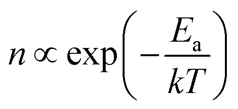 , n = number of nuclei, k = Boltzmann constant, T = temperature, Ea = activation energy).33 Fig. 3f shows an Arrhenius plot of α-phase grain density with a slope corresponding to an Ea value of ∼0.16 eV, indicating a low activation energy for the nucleation of α phase. Notably, the calculated activation energy is significantly lower than those reported for the nucleation in other ALD processes (0.5–1.4 eV),34,35 suggesting that the α phase nucleation proceeds through a distinct mechanism. The larger grain size of the α phase and increased GPC at high temperatures corroborate that the growth mechanism of the α phase differs from that of the β phase. The lower Ea in this work may indicate the heterogeneous nucleation of the α phase from the β phase matrix, but further clarification is necessary in future work.
Deposition mechanism of MnTe ALD
A detailed analysis of the correlation between substrate- and temperature-dependent deposition behavior provides insights into the underlying deposition mechanism. During the ALD of chalcogenide films, adjacent chalcogenide-H groups can react and form bridges.36,37 In this study, the co-injection of NH3 with the Te precursor is expected to produce intermediate H2Te precursors and form Te–H surface groups after the reaction. Due to the larger atomic size of Te compared to lighter chalcogenide elements, the Te–H bond is weaker than other chalcogenide–H bonds.38 Consequently, bridging reactions between Te–H surface groups are likely to occur even at low temperatures, leading to two distinct forms of Te on the surface: Te–H surface groups and bridged Te atoms. Fig. 4a shows the expected bridging reaction between adjacent Te–H surface groups and the resulting surface species. Therefore, when the polar Mn precursor is injected, different bonding mechanisms can occur depending on these two surface states.36 First, conventional ligand exchange reactions between the Mn precursor and the Te–H surface groups can occur when the surface retains a high density of the Te–H surface group. In contrast, the Mn precursor can bond to the bridged Te atoms without ligand removal through a Lewis base acid-based reaction (coordination bonding) when the surface contains high bridged Te atom density. In this case, the Mn atom in the precursor acts as a Lewis acid, and the bridged Te atoms function as Lewis bases with their lone pair electrons. Hence, depending on the surface state, the ALD can occur through conventional ligand exchange or coordination bonding (Fig. 4b), significantly influencing the properties of the deposited film. Coordination bonding can provide more N(SiMe3)2 ligands as reaction sites after adsorption compared to ligand exchange reactions. As a result, an increased possibility of coordination bonding may result in higher GPC, faster grain growth, and larger grain sizes. Moreover, more Te ions bonded to Mn ions can promote crystallization into the α phase, where Mn ions are octahedrally coordinated with six Te ions, rather than the β phase, where Mn ions have four-fold tetrahedral coordination with Te ions. Therefore, the formation of additional Mn–Te bonds through coordination bonding favors the formation of the higher-coordinated α phase. These findings effectively explain the substrate- and temperature-dependent growth characteristics observed in MnTe ALD. Generally, the bridging reactions between adjacent surface chalcogenide–H surface groups are known to be promoted as the temperature increases.39,40 Therefore, higher temperatures enhance Te bridging and shift the dominant bonding mechanism toward coordination bonding, explaining the increased formation of the α phase on SiO2 substrate at higher temperatures.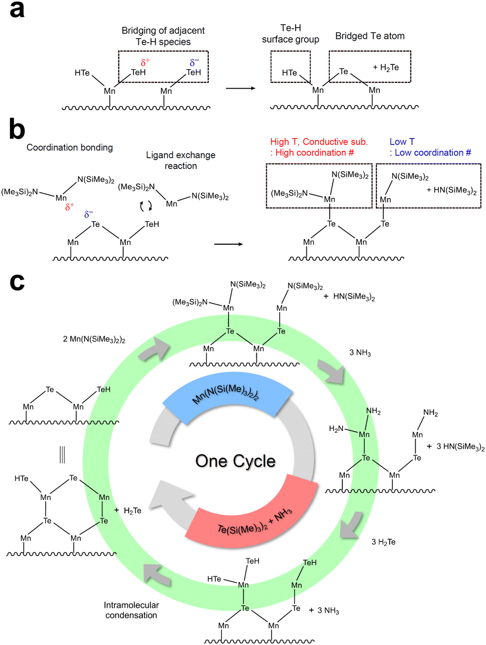 | ||
| Fig. 4 Schematic illustrations of surface reactions and deposition mechanisms during MnTe ALD: (a) Te bridging reaction between adjacent Te–H surface groups. (b) Two bonding mechanisms depending on surface states. (c) Proposed MnTe ALD deposition mechanism. | ||
Meanwhile, the α phase is deposited even at low temperatures on TiN substrate, which can be understood from the differences in substrate electrical conductivity. TiN substrate with their higher electrical conductivity compared to SiO2 can supply more electrons to the surface during deposition.41,42 Sufficient electron donation from the substrate could increase the electron density of Te atoms in Te–H surface groups, thereby enhancing the basicity of Te and promoting Te bridging reactions. DFT simulations were conducted to ascertain the electron density of Te atoms when MnTe was bonded to Si or Ti (Fig. S5, ESI†). The results showed a higher electron density for Te atoms when MnTe was bonded to Ti than Si. The increase in electron density at the Te atoms enhances the basicity of Te, making Te bridging more readily on conductive substrates and promoting the formation of the α phase at low temperatures. This enhanced chemical reaction also explains the higher GPC of the α-MnTe film on TiN than the β-MnTe on SiO2 at a low growth temperature of 100 °C, shown in Fig. 2a.
Fig. 4c presents the proposed mechanism explaining the deposition behavior of the MnTe ALD process. The schematic on the left side of Fig. 4c represents the initial surface state containing Te–H surface groups and bridged Te atoms. After injecting the Mn precursor, bonds between Mn and Te are formed through two bonding mechanisms. On SiO2 substrate, both bonding types are possible, but the conventional ligand exchange reaction mediated by the Te–H group is dominant at 100 °C. However, as temperature increases, the dominant surface reaction changes to coordinate bonding due to the enhanced Te bridging. On conductive TiN substrate, coordination bonding is dominant even at low temperatures because sufficient Te bridges are formed through electron donation. Subsequently, when NH3 and BTMS-Te are co-injected, two sequential reactions occur. First, NH3 reacts with surface N(SiMe3)2 groups and converts the surface to highly reactive NH2 groups by forming stable HN(SiMe3)2 (hexamethyldisilazane, HMDS) as by-products. This conversion is particularly significant for coordination bonding, where NH3 converts two bulky N(SiMe3)2 groups with sterically unhindered NH2 groups, enabling both ligands to participate in subsequent reactions. Next, highly reactive H2Te, generated by the reaction between BTMS-Te and NH3, reacts with surface NH2 groups to form NH3 and Te–H groups. Subsequently, intramolecular condensation occurs, maintaining the 1:1 composition of the film. Meanwhile, the consistent growth rate, composition, and crystal structure with varying Mn canister temperatures suggest that the MnTe ALD process does not involve physisorption or the formation of complex intermediates, confirming its feasible ALD process (Fig. S6, ESI†).
Impurity and conformality analysis
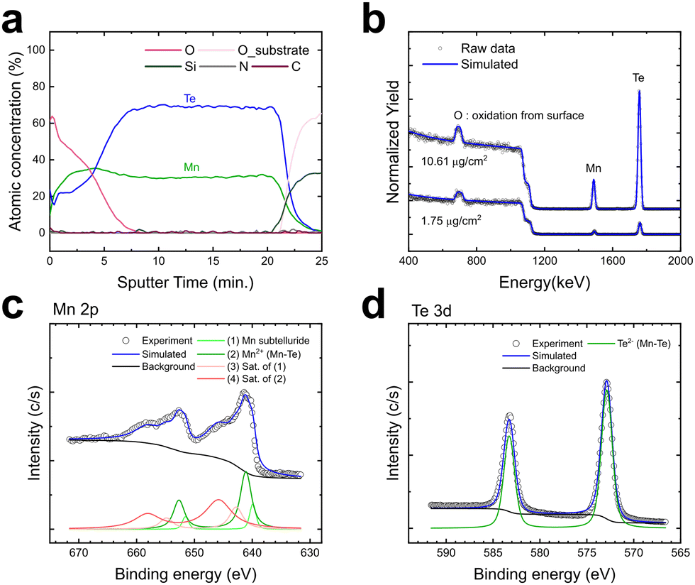
Chemical elements in the film were analyzed to evaluate the quality of the deposited MnTe film. Due to the strong oxidizing nature of manganese, MnTe films can quickly oxidize during deposition, even under high vacuum conditions.18,43,44 Also, impurity incorporation can be particularly problematic in low-temperature ALD processes, where insufficient thermal energy may hinder complete ligand exchange or by-product desorption. Fig. 5a shows the AES depth profile analysis of a ∼100 nm β-MnTe film deposited on SiO2 substrate grown at 100 °C. It should be noted that the quantitative composition ratios are not precise due to the lack of accurate references, and only the relative variations are meaningful. The results indicate no detectable impurities, such as C, N, or Si, across the film. Only a high O concentration was found on the film surface due to the exposure of the sample to air before the AES analysis. This finding also confirms that the stabilization of the wurtzite phase in MnTe was not attributed to doping effects from impurity elements such as nitrogen.45 The high purity of ALD-deposited MnTe films can be attributed to the high stability of HMDS,46 the reaction by-product, suggesting that TMSA ligand-based precursors are suitable for depositing high-purity metal chalcogenide films at low temperatures. The additional quantitative film composition of two films with different thicknesses was measured with RBS (Fig. 5b) to complement the AES analysis. Films with low (1.75 μg cm−2) and high (10.61 μg cm−2) LDs deposited on SiO2 were analyzed. Open circles represent raw data, while lines show simulation results. The RBS-derived LDs (1.28 × 10¹⁶ atom cm−2 and 6.68 × 10¹⁶ atom cm−2) and compositions of each sample (Mn0.5Te0.48 and Mn0.48Te0.5) confirmed a 1:1 stoichiometry regardless of film thickness, consistent with the XRF results. Additionally, the absence of peaks from any impurity elements, except for the surface oxygen, demonstrates the high purity of the films.
 | ||
| Fig. 5 (a) AES depth profile of the MnTe film on SiO2 grown at 100 °C. (b) RBS spectrum of films with layer densities of 1.75 and 10.61 μg cm−2. (c) Mn 2p and (d) Te 3d XPS spectra of the MnTe film on SiO2 grown at 100 °C. | ||
The chemical nature of the deposited film was further examined through XPS analysis. Fig. 5c and d show the XPS spectra of the Mn 2p and Te 3d orbitals obtained after 1.5 minutes of Ar+ ion sputtering to mitigate surface oxidation effects. Although there are no reported XPS results for the β-MnTe, the XPS spectra were deconvoluted and fitted based on reported parameters for other MnTe crystal structures.47,48 The spectra revealed that the Mn 2p peak consists of Mn sub-telluride at 639.9 eV originating from the surface region under high vacuum conditions of XPS analysis, the Mn2+ peak from Mn–Te bonding at 641.1 eV in the film bulk region, and satellites at 642.8 eV, and 645.8 eV, consistent with the literature values for MnTe. The Te 3d peak at 572.8 eV was attributed to a single electron state of Te2− in Mn–Te bonding. These results indicate that the deposited film has effectively formed the desired Mn–Te bonds. Furthermore, the XPS results of the C 1s, N 1s, and Si 2p orbitals (Fig. S7a–c, ESI†) confirmed the absence of impurities in the film, consistent with the AES results. The high purity of the films also suggests the potential for achieving a dense film structure. Fig. S8 (ESI†) shows the XRR spectra and the fitting results of β-MnTe films on SiO2 substrate deposited at 100 °C. The bulk density of the film was 4.19 g cm−3, approximately 91% of the theoretical density of β-MnTe (4.59 g cm−3).7 This high density indicates the formation of a well-crystallized film structure, even at low deposition temperatures.
Fig. 6a–d show the cross-sectional TEM images and EDS mapping results of a focused ion beam (FIB) milled sample deposited at 100 °C on a high aspect ratio (AR) structure with an opening diameter of ∼100 nm and a depth of ∼2900 nm (AR 1:29). Fig. 6a presents a TEM image of the entire hole structure. EDS mapping results of the top, middle, and bottom parts are shown in Fig. 6b, indicating uniform deposition over the entire surface and a consistent 1:1 ratio throughout the deep hole. The considerable presence of Mn and Te in the middle regions of both the top and middle sections can be attributed to the Mn and Te atoms detected from the back-side walls of the hole of the TEM specimen. The local atomic compositions calculated by the EDS are summarized in Table S3 (ESI†). Thickness analysis from the TEM images showed a uniform ∼15 nm thick film at the hole's top, middle, and bottom parts (Fig. 6c). Fig. 6d shows a magnified TEM image and FFT analysis, confirming the β phase crystallinity, consistent with the XRD results. This TEM analysis demonstrates that highly uniform film deposition is achievable even on extremely high aspect ratio structures, indicating excellent conformality of the MnTe ALD process.
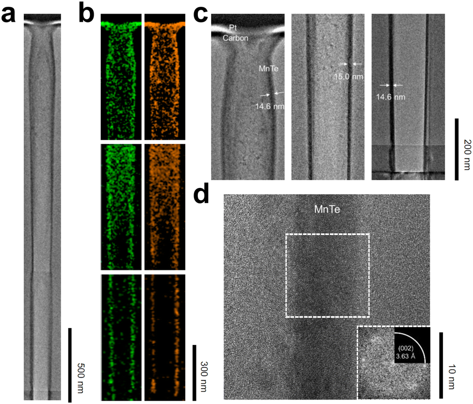 | ||
| Fig. 6 (a) Cross-sectional TEM image and (b) EDS analysis result of the MnTe films grown at high aspect ratio structures (100 °C). (c) TEM images of the top, middle, and bottom parts for measuring thickness. (d) Magnified image of the middle part of the hole. The inset image is a local FFT diffraction pattern obtained from the area in the white box. | ||
Annealing tests of β-MnTe films for PCM applications
Structure and electrical property variations by thermal annealing were examined to assess the potential PCM application of the deposited β-MnTe films. A 50 nm β-MnTe film was deposited on SiO2 substrate at 100 °C, capped with 100 nm W layer, and annealed under an Ar atmosphere from room temperature to 550 °C at a rate of 10 °C s−1. After annealing, the sample was cooled back to room temperature, and its crystallinity was analyzed. Fig. 7a shows the GAXRD patterns of the W-capped MnTe film before and after annealing. Fig. S9a (ESI†) shows the wide-range-GAXRD patterns. After annealing, the (002) plane peak from the β phase completely disappeared, while the (002) plane peak from the α phase emerged, with no other peaks from other planes of the α phase. This finding indicates that the film transformed into the α phase while maintaining the crystal alignment of the original β phase through a displacive transformation during annealing. The inset figure of Fig. 7a shows the atomic arrangement of the β- and α-MnTe films with their c-axis aligned to the out-of-plane direction. Such a structural transition is beneficial for PCM applications based on the displacive transformation, which may require much lower energy consumption than the conventional melt-quenching mechanism of Ge–Sb–Te alloy materials.6 Fig. 7b shows electrical resistance measurements of the MnTe film as a function of annealing temperature. A significant electrical resistance decrease was observed at ∼440 °C, corresponding to the structural transition temperature from the β phase to the α phase via displacive transformation.7 This large resistance change also highlights the potential of ALD MnTe films for high-performance PCM device applications utilizing displacive transformation.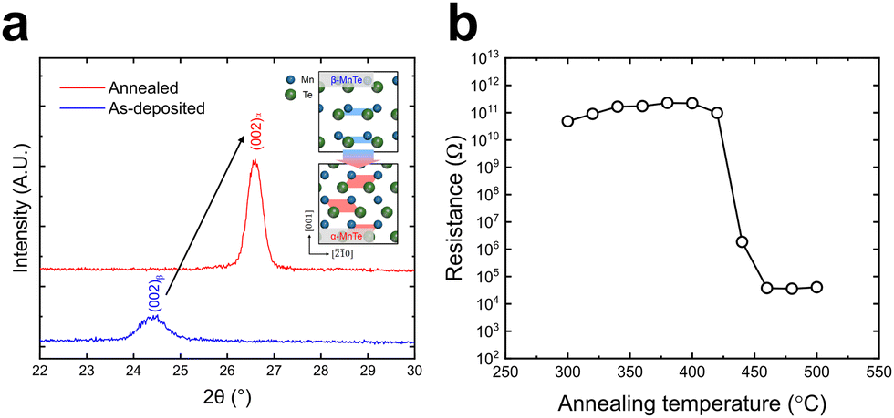 | ||
| Fig. 7 (a) GAXRD results of as-deposited and annealed MnTe films with a W capping layer. (b) Temperature dependence of resistance of the as-deposited MnTe film. Heating rate = 10 °C min−1. | ||
Nonetheless, forming the metastable β phase only on the SiO2 substrate invokes a concern about its formation on the metallic contact holes, typically TiN, in the PCM device structure. However, this issue can be resolved by adopting a thin insulating tunneling barrier between the TiN contact and the phase change material in the PCM device. Fig. S9b (ESI†) shows the GAXRD pattern of the 50 nm MnTe film grown at 100 °C on ∼1.5 nm SiO2/50 nm TiN substrate. The GAXRD data reveals that the film comprises the β phase due to the thin SiO2's block of charge supply from the TiN under no effective bias application during the ALD. Nonetheless, such a thin SiO2 layer does not block electrical conduction during the PCM device operation conditions,49,50 demonstrating the feasibility of MnTe ALD for PCM applications.
Conclusions
This study demonstrated a strategic approach to depositing metastable β-MnTe films at low temperatures through a carefully designed ALD process. The key to achieving a metastable phase at 100 °C was the combination of two strategies: the use of the nitrogen-coordinated Mn precursor (Mn(N(SiMe3)2)2) and co-injection of NH3 with the Te precursor (Te(Si(Me)3)2) to minimize contamination and ensure sufficient reactivity even at a growth temperature as low as 100 °C. This approach enabled the deposition of smooth nanocrystalline β-MnTe films with high purity, uniformity, and conformality, even on extreme three-dimensional hole structures. The phase evolution between the metastable (more insulating) β- and stable (more conducting) α-phases depended on substrate types and growth temperature. The metastable β-phase, desired for the low-power PCM application, could be achieved on the insulating SiO2 substrate at a low growth temperature of 100 °C. In contrast, the stable α phase was formed on electrically conducting TiN substrate at all temperatures from 100 to 160 °C or on SiO2 substrate at elevated temperatures (160 °C). DFT simulation provided the clue to understand such a variation. The conventional ALD mechanism, mediated by the surface Te–H group at low temperature and on insulating substrates, preferred to form the β-phase having a lower Te coordination number of Mn ions. However, another coordination bonding mediated ALD mechanism based on the Lewis acid–base reaction at the Te site with lone pair electrons is preferred at higher temperatures and on conducting substrates, resulting in the α-phase having a higher Te coordination number of Mn ions. Furthermore, annealing tests confirmed the potential of ALD-deposited MnTe for future PCM applications, utilizing the displacive transformation. This process design strategy provides valuable insights into the low-temperature ALD of other metastable-phase transition metal tellurides.Author contributions
G. J. designed and performed the experiments and analysis. J. J., W. K., D. K., and W. N. contributed to the analysis and provided insightful advice throughout the project. W. K., B. P., S. J., and S. K. participated in the hardware maintenance for the ALD equipment. G. J., C. Y., and C. S. H. wrote the manuscript. C. Y. and C. S. H. supervised the overall research.Data availability
The data supporting this article have been included as part of the ESI.† The data are available from the corresponding authors upon request.Conflicts of interest
There are no conflicts to declare.Acknowledgements
This work was supported by the National Research Foundation of Korea (2020R1A3B2079882) and the Technology Innovation Program (RS-2023-00234671) funded by the Ministry of Trade, Industry & Energy (MOTIE, Korea) (1415187506). The authors thank Air Liquide, Inc. for providing the Mn and Te precursors and Soulbrain, Inc. for supplying the Te precursor. XPS analysis of the films was conducted at the Research Institute of Advanced Materials (RIAM) of Seoul National University.References
- P. Wang, D. Yang and X. Pi, Adv. Electron. Mater., 2021, 7, 2100278 CrossRef CAS.
- S. Lee, S. Lee, S. Jung, J. Jung, D. Kim, Y. Lee, B. Seok, J. Kim, B. G. Park, L. Šmejkal, C. J. Kang and C. Kim, Phys. Rev. Lett., 2024, 132, 036702 CrossRef CAS PubMed.
- M. E. Schlesinger, J. Phase Equilib., 1998, 19, 591–596 CrossRef CAS.
- S. Mori, Y. Sutou, D. Ando and J. Koike, Mater. Trans., 2018, 59, 1506–1512 CrossRef CAS.
- M. Kim, S. Mori, Y. Shuang, S. Hatayama, D. Ando and Y. Sutou, Phys. Status Solidi RRL, 2022, 16, 2100641 CrossRef CAS.
- S. Mori, D. Ando and Y. Sutou, Mater. Des., 2020, 196, 109141 CrossRef CAS.
- S. Mori, S. Hatayama, Y. Shuang, D. Ando and Y. Sutou, Nat. Commun., 2020, 11, 85 CrossRef CAS PubMed.
- S. Siol, Y. Han, J. Mangum, P. Schulz, A. M. Holder, T. R. Klein, M. F. A. M. Van Hest, B. Gorman and A. Zakutayev, J. Mater. Chem. C, 2018, 6, 6297–6304 RSC.
- Y. Han, R. Trottier, S. Siol, B. Matthews, M. Young, C. B. Musgrave, S. Lany, J. Tate, Q. Zhang, A. M. Holder and A. Zakutayev, Phys. Rev. Appl., 2020, 13, 014012 CrossRef CAS.
- Y. Han, A. M. Holder, S. Siol, S. Lany, Q. Zhang and A. Zakutayev, J. Phys. Chem. C, 2018, 122, 18769–18775 CrossRef CAS.
- S. Siol, A. Holder, J. Steffes, L. T. Schelhas, K. H. Stone, L. Garten, J. D. Perkins, P. A. Parilla, M. F. Toney, B. D. Huey, W. Tumas, S. Lany and A. Zakutayev, Sci. Adv., 2018, 4, eaaq1442 CrossRef PubMed.
- Y. K. Lee, C. Yoo, W. Kim, J. W. Jeon and C. S. Hwang, J. Mater. Chem. C, 2021, 9, 3708–3725 RSC.
- R. W. Johnson, A. Hultqvist and S. F. Bent, Mater. Today, 2014, 17, 236–246 CrossRef CAS.
- T. H. Hong, H. W. Kim, Y. S. Kim, H. J. Jeong, S. B. Cho and J. S. Park, Chem. Mater., 2023, 35, 5168–5176 CrossRef CAS.
- Y. Kim, W. J. Woo, D. Kim, S. Lee, S. Min Chung, J. Park and H. Kim, Adv. Mater., 2021, 33, 2005907 CrossRef CAS PubMed.
- Z. Guo, R. Zhao, S. Yan, W. Xiong, J. Zhu, K. Lu and X. Wang, Chem. Mater., 2021, 33, 2478–2487 CrossRef CAS.
- P. O. Oviroh, R. Akbarzadeh, D. Pan, R. A. M. Coetzee and T. C. Jen, Sci. Technol. Adv. Mater., 2019, 20, 465–496 CrossRef PubMed.
- N. Kunitomi, Y. Hamaguchi and S. Anzai, J. Phys., 1964, 25, 568–574 CrossRef CAS.
- H. C. M. Knoops, S. E. Potts, A. A. Bol and W. M. M. Kessels, Handbook of Crystal Growth: Thin Films and Epitaxy: Second Edition, Elsevier Inc., 2015, vol. 3, pp. 1101–1134 Search PubMed.
- V. K. Dixit, K. Neishi, N. Akao and J. Koike, IEEE Trans. Device Mater. Reliab., 2011, 11, 295–302 CAS.
- M. P. Clark, T. Muneshwar, M. Xiong, K. Cadien and D. G. Ivey, ACS Appl. Nano Mater., 2019, 2, 267–277 CrossRef CAS.
- Database of ALD processes, https://www.atomiclimits.com/alddatabase/, (accessed November 2024).
- F. Mattelaer, P. M. Vereecken, J. Dendooven and C. Detavernier, Chem. Mater., 2015, 27, 3628–3635 CrossRef CAS.
- H. E. Nieminen, V. Miikkulainen, D. Settipani, L. Simonelli, P. Hönicke, C. Zech, Y. Kayser, B. Beckhoff, A. P. Honkanen, M. J. Heikkilä, K. Mizohata, K. Meinander, O. M. E. Ylivaara, S. Huotari and M. Ritala, J. Phys. Chem. C, 2019, 123, 15802–15814 CrossRef CAS.
- V. Miikkulainen, A. Ruud, E. Østreng, O. Nilsen, M. Laitinen, T. Sajavaara and H. Fjellvaìšg, J. Phys. Chem. C, 2014, 118, 1258–1268 CrossRef CAS.
- M. Wilken, A. Muriqi, A. Krusenbaum, M. Nolan and A. Devi, Chem. Eur. J., 2024, 30, e202401275 CrossRef CAS PubMed.
- R. A. Andersen, K. Faegri, J. C. Green, A. Haaland, M. F. Lappert, W. Leung and K. Rypdal, Inorg. Chem., 1988, 27, 1782–1786 CrossRef CAS.
- T. Gwon, T. Eom, S. Yoo, H. K. Lee, D. Y. Cho, M. S. Kim, I. Buchanan, M. Xiao, S. Ivanov and C. S. Hwang, Chem. Mater., 2016, 28, 7158–7166 CrossRef CAS.
- C. Yoo, W. Kim, J. W. Jeon, E. S. Park, M. Ha, Y. K. Lee and C. S. Hwang, ACS Appl. Mater. Interfaces, 2020, 12, 23110–23118 CrossRef CAS PubMed.
- E. S. Park, C. Yoo, W. Kim, M. Ha, J. W. Jeon, Y. K. Lee and C. S. Hwang, Chem. Mater., 2019, 31, 8663–8672 CrossRef CAS.
- E. S. Park, C. Yoo, W. Kim, M. Ha, J. W. Jeon, T. Eom, Y. K. Lee and C. S. Hwang, Chem. Mater., 2019, 31, 8752–8763 CrossRef CAS.
- Y. K. Lee, E. S. Park, C. Yoo, W. Kim, J. W. Jeon, M. Ha and C. S. Hwang, Cryst. Growth Des., 2020, 20, 4649–4656 CrossRef CAS.
- N. E. Richey, C. De Paula and S. F. Bent, J. Chem. Phys., 2020, 152, 040902 CrossRef CAS PubMed.
- J. P. Wooding, S. A. Gregory, A. Atassi, G. Freychet, K. Kalaitzidou and M. D. Losego, At. Layer Deposition, 2023, 1, 1–18 CrossRef.
- W. J. Lee and M. H. Hon, J. Phys. Chem. C, 2010, 114, 6917–6921 CrossRef CAS.
- S. C. Riha, A. A. Koegel, X. Meng, I. S. Kim, Y. Cao, M. J. Pellin, J. W. Elam and A. B. F. Martinson, ACS Appl. Mater. Interfaces, 2016, 8, 2774–2780 CrossRef CAS PubMed.
- C. Goehry and N. Schneider, J. Phys. Chem. C, 2017, 121, 5871–5881 CrossRef CAS.
- T. L. Cottrell, The Strengths of Chemical Bonds, Academic Press, 1954 Search PubMed.
- A. Comas-Vives, Phys. Chem. Chem. Phys., 2016, 18, 7475–7482 RSC.
- X. Rozanska, F. Delbecq and P. Sautet, Phys. Chem. Chem. Phys., 2010, 12, 14930–14940 RSC.
- S. W. Lee, B. J. Choi, T. Eom, J. H. Han, S. K. Kim, S. J. Song, W. Lee and C. S. Hwang, Coord. Chem. Rev., 2013, 257, 3154–3176 CrossRef CAS.
- J. W. Jeon, C. Yoo, W. Kim, W. Choi, B. Park, Y. K. Lee and C. S. Hwang, Dalton Trans., 2022, 51, 594–601 RSC.
- M. Hasegawa, Ellingham Diagram, Elsevier Ltd, 2013, vol. 1 Search PubMed.
- H. C. Shomate, J. Am. Chem. Soc., 1943, 65, 785–790 CrossRef.
- T. H. Culman, R. Woods-Robinson, J. S. Mangum, R. W. Smaha, C. L. Rom, A. Zakutayev and S. R. Bauers, J. Mater. Chem. C, 2022, 10, 15806–15815 RSC.
- X. Liu, J. Zhang, A. Vazquez, D. Wang and S. Li, J. Phys. Chem. A, 2019, 123, 10520–10528 CrossRef CAS PubMed.
- R. J. Iwanowski, M. H. Heinonen and B. Witkowska, J. Alloys Compd., 2010, 491, 13–17 CrossRef CAS.
- R. J. Iwanowski, M. H. Heinonen and E. Janik, Chem. Phys. Lett., 2004, 387, 110–115 CrossRef CAS.
- R. Zhang, Y. Hu, Q. Chou, T. Lai and X. Zhu, J. Alloys Compd., 2019, 798, 342–349 CrossRef CAS.
- B. Chen, X. P. Wang, F. Jiao, L. Ning, J. Huang, J. Xie, S. Zhang, X. Bin Li and F. Rao, Adv. Sci., 2023, 10, 2301043 CrossRef CAS PubMed.
Footnote |
| † Electronic supplementary information (ESI) available. See DOI: https://doi.org/10.1039/d4tc05499g |
| This journal is © The Royal Society of Chemistry 2025 |