
 Open Access Article
 This Open Access Article is licensed under a Creative Commons Attribution-Non Commercial 3.0 Unported Licence
Enhancing optoelectronic performance of organic phototransistors through surface doping of tetra-bromo perylene diimide single crystals†
Huagui
Zhuo‡
a,
Ye In
Cho‡
b,
Ke
Gao
a,
Zhiwei
Wang
a,
Zhenping
Li
a,
Xingshuo
Chu
a,
Tianhang
Cui
a,
Wanuk
Choi
c,
Gang
Chang
d,
Jaeyong
Ahn
 *b,
Xiaobo
Shang
*a and
Joon Hak
Oh
*b
*b,
Xiaobo
Shang
*a and
Joon Hak
Oh
*b
aState Key Laboratory for Mechanical Behavior of Materials, Shaanxi International Research Center for Soft Matter, School of Materials Science and Engineering, Xi’an Jiaotong University, Xi’an 710049, P. R. China. E-mail: xiaoboshang@xjtu.edu.cn
bSchool of Chemical and Biological Engineering, Institute of Chemical Processes, Seoul National University, 1 Gwanak-ro, Gwanak-gu, Seoul 08826, Republic of Korea. E-mail: jaeyongahn@snu.ac.kr; joonhoh@snu.ac.kr
cCenter for Ordered Nanoporous Materials Synthesis, School of Environmental Science and Engineering, POSTECH, Pohang, Gyeongbuk 37673, Republic of Korea
dInstrumental Analysis Center of Xi'an Jiaotong University, Xi’an 710049, P. R. China
First published on 13th March 2025
Abstract
Organic phototransistors (OPTs) built from organic single crystals offer distinct advantages over their thin-film counterparts due to their superior charge transport, large surface area, and defect-free molecular arrangement. However, the progress in developing high-performance n-type organic semiconductors has largged behind that of p-type materials, posing a challenge to the advancement of organicelectronic devices. To address this issue, we synthesized novel tetra-bromo-substituted chiral perylene diimides, which self-assembled into single crystals, offering potential of n-type semiconductors. Traditional doping techniques often risk damaging the delicate crystal structure; therefore, we implemented a mild surface doping method using aniline vapor, which preserves the structural integrity of the crystals while significantly enhancing their optoelectronic properties. The doped devices exhibited a remarkable improvement in charge transport, with electron mobility increasing four times to 1.19 × 10⁻² cm2 V−1 s−1. Furthermore, the optoelectronic characteristics were significantly improved simultaneously, with the external quantum efficiency increasing over two-fold, and response times becoming notably faster. These enhancements are attributed to the increased charge carrier density and improved exciton separation efficiency following doping. This study demonstrates that our surface doping strategy is a highly effective approach for optimizing the performance of organic single-crystal OPTs, providing a promising pathway for future applications in advanced optoelectronic devices.
Introduction
Organic field-effect transistors (OFETs) offer the advantages of flexibility, low-cost fabrication, lightweight and compatibility with bendable substrates, making them ideal for applications in flexible displays, wearable electronics, and low-power sensors.1,2 Their unique properties also enable diverse applications such as e-paper and organic circuits, pushing the boundaries of conventional electronics into new, innovative devices.3 Among them, organic phototransistors (OPTs) have great potential due to their high gain characteristics, amplifying weak light signals into substantial electrical currents for enhanced photodetection sensitivity.4 In the field of OPTs, the integration of micro- or nanoscale single-crystal organic semiconductors (OSC) as the active layer has been demonstrated to markedly enhance device performance. This improvement is attributed to their defect-free nature from high crystallinity, which enables the semiconductors to achieve intrinsic high charge carrier mobility.5–7 This approach not only facilitates the realization of OPTs with superior photoconversion efficiency but also extends their operational stability,8 positioning them as a promising platform for next-generation photodetection technologies.Perylene diimides (PDIs), featuring an extensive π-conjugated system, commendable thermal stability, and elevated carrier mobility, stand out as an exceptional n-type semiconductor material.9–12 In particular, the synthetic route of PDI molecules is relatively mature and can be chemically modified to introduce various functional groups to meet the needs of specific applications.13–17 Substitution on ortho/bay/imide position of PDIs can effectively tune the optoelectronic properties and solubility of PDIs.18,19 Compared with p-type organic semiconductors, the development of n-type organic semiconductors has relatively lagged behind. However, their indispensable role in achieving high-efficiency and multi-functional organic electronic devices is becoming increasingly prominent.20,21 The unique properties of PDIs, such as their high electron affinity and stability, make them indispensable for the realization of advanced electronic functionalities, particularly in devices that require efficient electron transport and robust performance under operational stress.22,23
Doping in organic semiconductors represents a valuable and effective strategy to modulate the electrical characteristics of materials, thereby enhancing the performance of electronic devices fabricated from these materials.24 By incorporating extrinsic atoms or molecules, the process of doping can significantly augment carrier concentration, refine carrier mobility, and bolster material conductivity.25 Among various doping methods including co-processing and sequential doping, surface vapor doping is an attractive strategy because it has less negative impact on the crystallinity and morphology of the underlying active layer.5 In recent research, several notable works on surface doping have been reported. In pentacene-based OFETs, surface doping via forming specific heterojunctions show differences in IDS instability between doped and undoped devices, indicating faster carrier-trapping near the gate dielectric. It also shows that proper surface doping can enhance operating stability.26 Takeya et al. proposed a strategy for surface functionalization of single crystal OSC. Charge transfer at the surface formed a 2D electronic system, enabling a conductive nanosheet with good properties while keeping the crystal structure. Doping optimization gave a stable nanosheet.27 Compared with the above-mentioned heterojunction doping and surface solution doping, surface vapor doping is beneficial to regulate energy levels, promote electron transfer, and improve the mobility of devices. Through the surface vapor doping, fine-tuning of energy levels makes organic semiconductors as optimal candidates for the active layers in optoelectronic devices. n-Type doping and p-type doping are the two fundamental doping types in semiconductor materials, each introducing different types of charge carriers.28 The growing demand for high-performance n-type semiconductors is driven by the need to realize complementary circuits or dual-carrier devices, which require a balanced distribution of carrier types and superior electron transport capabilities.29 The development of advanced doping techniques for n-type organic semiconductors is therefore critical for the advancement of next-generation electronic devices,30–33 offering the potential to unlock new functionalities and performance benchmarks.
In this work, we present the synthesis and self-assembly process of a tetra-bromine-substituted PDI derivative, (S)-4Br-PDI-Ph. The crystal structures and optoelectronic characteristics of this material were studied through X-ray diffraction (XRD) analysis and device performance measurements. The pristine (S)-4Br-PDI-Ph single-crystal based OFETs demonstrated an average electron mobility of 2.93 × 10⁻³ cm2 V−1 s−1. Following surface doping with aniline, the mobility was significantly enhanced to 1.19 × 10⁻² cm2 V−1 s−1. Additionally, the doped OFETs showed improved photodetection capabilities, with an external quantum efficiency (EQE) reaching 2200% and a specific detectivity (D*) as high as 9.7 × 10¹¹ jones, alongside a faster response time of approximately 0.6 s. These findings underscore the effectiveness of a straightforward doping strategy for boosting the performance of organic optoelectronic devices.
Experimental section
Synthesis of chiral semiconductors and self-assembly for nanowires
For the synthesis of (S)-4Br-PDI-Ph compounds, 1,6,7,12-tetrabromoperylene dianhydride (4Br-PTCDA) (5.28 g, 7.46 mmol, 1 equiv.) and (S)-1-phenylethylamine (3.62 g, 29.83 mmol, 4 equiv.) were taken in a round-bottomed flask equipped with a water-condenser. Thereafter, propionic acid (100 mL) was added. Under argon atmosphere, the reaction mixture was refluxed under stirring for 24 h, cooled to room temperature. The precipitate was filtered off, thoroughly washed with several portions of water and ethanol, and dried to obtain the crude product. The crude product was purified by silica gel column chromatography with dichloromethane (DCM):hexane 2:1 as eluent. Single crystal of (S)-4Br-PDI-Ph were prepared under a mixed solvent system using the solubility difference between the solvents, DCM and methanol (MeOH). A 1 mg mL−1 solution of (S)-4Br-PDI-Ph in DCM was first prepared by dissolving the compound under ultrasonication stirring at room temperature. Then 1 mL of MeOH was added to 1 mL of this solution, and the resulting mixture was put into a sealed vial. After three or four days, the single crystals were formed through the self-assembly. For crystal analysis, crystals were formed in toluene solution by diffusion of nonsolvent MeOH.Materials analysis
The 1H NMR and 13C NMR spectra were measured on a Bruker Avance III (Ultrashield Plus 400 MHz magnet) spectrometer using tetramethylsilane as the internal standard. Absorption spectra were recorded using a V-770 UV-vis-NIR spectrophotometer (JASCO). Microscopic crystal morphologies were measured using field emission scanning electron microscopy (FE-SEM, JEOL JSM-7800F Prime) after 1![[thin space (1/6-em)]](https://www.rsc.org/images/entities/char_2009.gif) min of Pt sputtering. Cyclic voltametric (CV) measurements were performed using a three-electrode cell with a polished 2 mm glassy carbon as working electrode, Pt as counter electrode and Ag/AgNO3 as reference electrode. The solution was prepared in chloroform with 1 × 10⁻⁴ M concentration of (S)-4Br-PDI-Ph and 0.1 M of supporting electrolyte, tetrabutylammonium hexafluorophosphate. In order to calculate the lowest unoccupied molecular orbital (LUMO) level, the redox data were standardized to the ferrocene/ferrocenium couple having a calculated absolute energy of −4.8 eV, using a following equation. The highest occupied molecular orbital (HOMO) level was calculated using the optical band gap of UV-vis spectra.
min of Pt sputtering. Cyclic voltametric (CV) measurements were performed using a three-electrode cell with a polished 2 mm glassy carbon as working electrode, Pt as counter electrode and Ag/AgNO3 as reference electrode. The solution was prepared in chloroform with 1 × 10⁻⁴ M concentration of (S)-4Br-PDI-Ph and 0.1 M of supporting electrolyte, tetrabutylammonium hexafluorophosphate. In order to calculate the lowest unoccupied molecular orbital (LUMO) level, the redox data were standardized to the ferrocene/ferrocenium couple having a calculated absolute energy of −4.8 eV, using a following equation. The highest occupied molecular orbital (HOMO) level was calculated using the optical band gap of UV-vis spectra.
Fabrication of OPTs
Heavily doped silicon wafers (n-type, <0.004 Ω cm) with thermally grown 300-nm-thick SiO2 (Ci = 11.5 nF cm−2) were used as substrates for fabricating OPTs. The n-octadecyltrimethoxysilane (OTS) solution was formed by dissolving 10 μL of OTS in 10 mL trichloroethylene. The SiO2/Si wafers were cleaned with piranha solution for 30 min (a mixture of 75 vol% H2SO4 and 25 vol% H2O2), followed by UV-ozone treatment. Then, OTS solution was spin-coated at 1500 rpm for 30 s onto the wafers, and then the samples were kept overnight in a vacuum desiccator with a separate vial containing a few drops of ammonia solution. The wafers were sequentially washed with toluene, acetone and isopropyl alcohol, and dried with nitrogen blowing. The fabricated single crystals were filtered and dispersed in ethanol. The crystal dispersion was carefully drop-casted onto OTS-treated SiO2/Si substrates, and thermally annealed at 60 °C in a vacuum oven to remove the residual solvent. Source and drain gold electrodes (150 nm) were thermally evaporated under high vacuum condition (<5 × 10⁻⁶ torr).Optoelectrical measurements
The current–voltage characteristics of the OFETs were measured inside a vacuum chamber (<5.0 × 10⁻² torr), by using a Keithley 4200-SCS semiconductor parametric analyzer. A 532 nm monochromatic light was obtained from Oriel Cornerstone 130 1/8 m monochromator.Computational methods for energy level
The structures were optimized by using density functional theory (DFT) in a vacuum environment, employing the Gaussian 16 software,34 the vibrational frequencies were calculated after geometries optimization and no imaginary frequency was found. The structure optimization, frequency analysis and the energy levels for the frontier molecular orbitals were obtained at the Becke three-parameter Lee–Yang–Parr (B3LYP)35 functional combining with 6-31G(d)36 basis set, and no imaginary frequency was found.Results and discussion
Synthesis of chiral organic semiconductors and their self-assembly for nanowire fabrication
(S)-4Br-PDI-Ph was synthesized from tetra-bromo PTCDA with (S)-1-phenylethylamine (the details are described in Experimental section).37 The product was purified by chromatography on silica gel with eluent of DCM/hexane and recrystallized from a solvent mixture of DCM and MeOH to give (S)-4Br-PDI-Ph (Fig. 1a). Based on CV analysis (Fig. S1, ESI†) and DFT calculations (Fig. 1b), synthesized (S)-4Br-PDI-Ph has an energy band gap comparable to that of conventional bay-substituted PDI materials.32 The HOMO and LUMO energy levels of the molecule are determined to be −6.28 eV and −3.72 eV in DFT calculation and −6.16 eV and −3.96 eV in CV analysis, respectively, indicating a well-defined electronic structure suitable for optoelectronic applications. As shown in Fig. 1c, the absorbance spectrum of (S)-4Br-PDI-Ph dissolved in DCM (10−4 M) exhibited distinct peaks in the visible wavelength range. Four main absorption peaks were observed at 532, 499, 441, and 420 nm, corresponding to the 0-0, 0-1, 0-2, and 0-3 vibronic transitions of the individual molecules, respectively. In contrast, the absorbance spectrum of the fabricated single crystals was red-shifted by approximately 7 nm compared to the solution, which can be attributed to the strong intermolecular interactions present in the solid-state. | ||
| Fig. 1 (a) Chemical structures of (S)-4Br-PDI-Ph. (b) Charge-density isosurfaces of the LUMO and HOMO of (S)-4Br-PDI-Ph monomer estimated from the DFT calculation. (c) UV-vis spectra of (S)-4Br-PDI-Ph in DCM solution (10−4 M) and its self-assembled single crystals deposited on a quartz plate. | ||
The morphological characteristics of (S)-4Br-PDI-Ph single crystals were investigated using scanning electron microscopy (SEM). As shown in Fig. 2a and Fig. S2 (ESI†), the resulting crystals are single-crystal nanowires with sizes ranging from 10 to 150 μm. To further understand the molecular arrangement of (S)-4Br-PDI-Ph, single-crystal XRD analysis was conducted to determine its crystal structure (Fig. 2b and c). The analysis revealed that (S)-4Br-PDI-Ph crystallizes in the triclinic C2 space group, with the molecule adopting a twisted backbone structure, analogous to the other bulk halogen-substituted or bay-substituted PDIs.9,38,39 The crystal structure of (S)-4Br-PDI-Ph single crystals was preserved after 5 min of aniline surface vapor doping, as indicated by the identical peaks observed in the powder X-ray diffraction measurements (Fig. S3, ESI†).
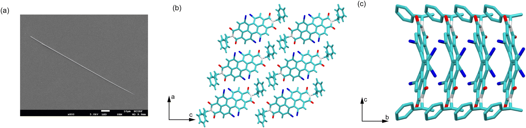 | ||
| Fig. 2 (a) A SEM image of (S)-4Br-PDI-Ph organic single crystal formed by diffusion of methanol into the toluene solution. Crystal structure of (S)-4Br-PDI-Ph; (b) b-axis projection, and (c) drawing of π–π stacking for the (S)-4Br-PDI-Ph. (d) Stacked layers of (S)-4Br-PDI-Ph shifted by half their short length, color code: N, light grey; O, red; Br, blue. | ||
Effect of surface doping on device performance
To investigate the optoelectronic properties of (S)-4Br-PDI-Ph single crystals before and after doping, OPTs with bottom-gate top-contact configurations were fabricated. Fig. 3a illustrates the schematic of the device structure and doping process. The optical microscope images of the fabricated OPT devices are illustrated in Fig. S2 (ESI†). Surface vapor doping was performed by treating the fabricated OPTs with aniline vapor. The OPT devices were exposed to saturated aniline vapor for 5 min at 50 °C under a nitrogen-filled closed space, therefore aniline vapor effectively adsorbed to single crystals surface and altered its electronic transport characteristics. As an n-type dopant, aniline interacts with semiconductor molecules, by donating electrons to increase the electron density (Fig. S4, ESI†).40 The long-range π-electron delocalization along the axis of the nanowires after aniline doping on the outer surface resulted in improvement of the charge carrier mobility and optoelectronic response of the crystals.41 Charge transport characteristics of individual single crystals were investigated using the fabricated OPTs under dark and vacuum condition (<10−2 torr). Fig. 3b, c and Fig. S5a (ESI†) show the transfer characteristics of (S)-4Br-PDI-Ph single crystal-based OPTs before and after doping. After doping, clear enhancement of electronic properties were observed, such as the negative shift of threshold voltage (VT) and a steeper slope. The average electron mobility increased over 4 times, from 2.93 × 10⁻³ cm2 V−1 s−1 to 1.19 × 10⁻² cm2 V−1 s−1. The maximum electron mobility could reach to 4.92 × 10⁻² cm2 V−1. In addition, the average threshold voltage negatively shifted from 12.5 V to 8.4 V, while maintaining a good an on/off ratio (Ion/Ioff) of over 103. Notably, our mild doping strategy not only improved the electrical performance but also preserved the on/off ratio of the OFETs and their operational stability. The output properties in Fig. 3d and Fig. S5b (ESI†) further support the doping effect. Compared with pristine devices, doped devices exhibited higher output currents under various gate voltages. This shows that through surface doping, the electron transport path is optimized, and the conductivity of the device is improved. This improvement may be attributed to the charge transfer interaction between aniline and (S)-4Br-PDI-Ph molecules, resulting in an adjustment of molecule energy levels and improved electron transport efficiency. The doping process also effectively eliminated electron traps at the crystal step edges, which would otherwise hinder charge transport.38 This is further supported by the calculated number of deep interface trap states (Ntrap) derived from the subthreshold region analysis,42| Ntrap = Ci|VT − Von|/e |
 | ||
| Fig. 3 (a) Schematic illustrations of fabricated OPT device and its doping process. Transfer characteristics of (b) pristine and (c) doped (S)-4Br-PDI-Ph single crystal based OPTs. (d) Output characteristics of pristine and doped (S)-4Br-PDI-Ph single crystal based OPTs. (e) UV-vis spectra of pristine and doped (S)-4Br-PDI-Ph single crystals. | ||
To further investigate the optoelectronic properties, the pristine and doped (S)-4Br-PDI-Ph single crystal based OPTs were illuminated with a 532 nm monochromatic light, which is near the absorption maximum. Both devices exhibited photodoping effects, characterized by an increase in source-drain current (IDS) and a negative shift in VT under light illumination (Fig. 4a and Fig. S6, ESI†). As the light intensity increased from 20 to 60 μW cm−2, a gradual rise of IDS and a negative shift of VT were observed, attributed to the trapping of photogenerated charge carriers. In addition, the doped crystals show more distinct photoresponses, suggesting improved charge carrier generation and transport efficiency due to the doping process. This enhancement can be attributed to the reduction of electron traps at the crystal surface and step edges, facilitating more efficient charge transfer. Key figures of merit, including EQE and D*, were calculated to evaluate and compare the photodetection properties of (S)-4Br-PDI-Ph single crystal-based OPTs before and after aniline doping, based on the transfer curves (Fig. 4b). The pristine OPTs demonstrated maximum EQE and D* values of 967% and 5.4 × 10¹¹ jones, respectively, under 20 μW cm−2 monochromatic light irradiation. After 5 mins of aniline doping, the devices exhibited significantly improved optoelectronic performance, with EQE and D* values reaching 2200% and 9.7 × 10¹¹ jones, respectively. This enhancement attributed to the increased charge carrier mobility, which improved exciton separation efficiency, thereby contributing to a higher photocurrent.
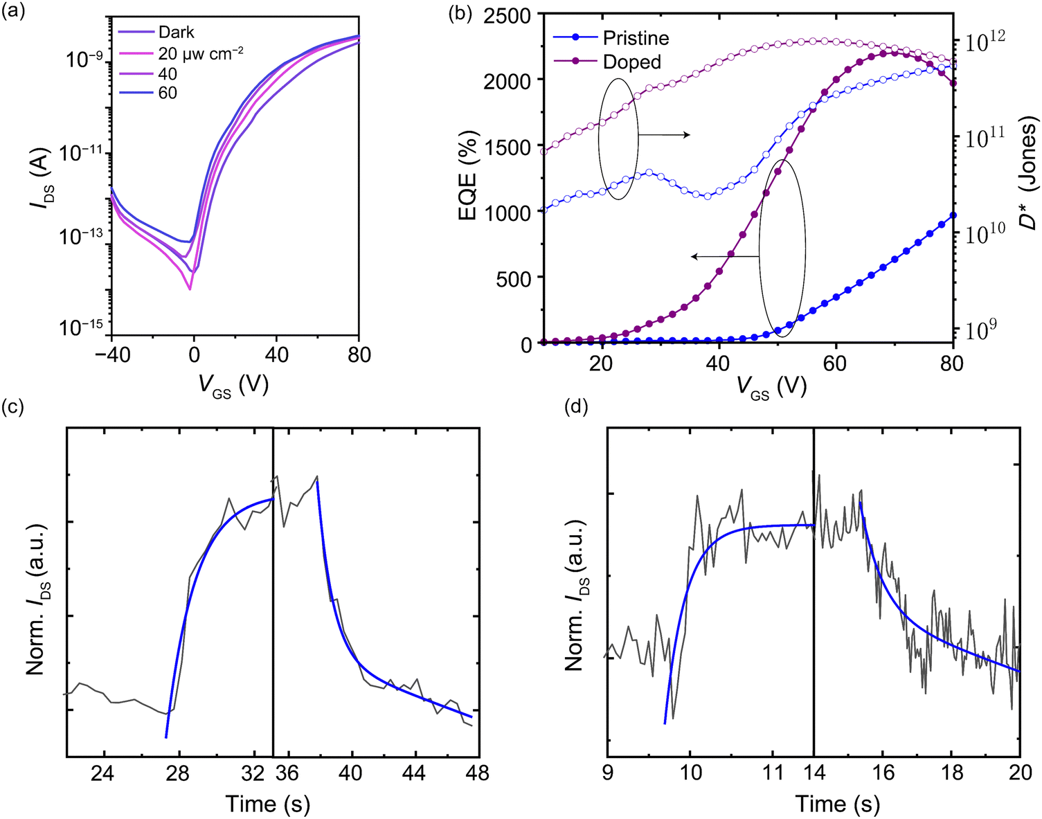 | ||
| Fig. 4 (a) Transfer characteristics of doped (S)-4Br-PDI-Ph single crystal based OPT under monochromatic light irradiation varying in intensity (λ = 532 nm). (b) EQE and D* results of pristine and doped (S)-4Br-PDI-Ph single crystal based OPTs. Photoresponse time of (d) pristine and (e) doped (S)-4Br-PDI-Ph single crystal based OPTs. All measurements were taken under vacuum conditions. | ||
Additionally, the photoresponse time measurements in Fig. 4c and d highlight the impact of doping on the device's dynamic performance upon monochromatic light irradiation. The rise and decay times are extracted from the time it takes for the current to rise from 10% to 90% and to fall from 90% to 10% under light illumination. The pristine single crystal based OPTs exhibit a slower response time, with a rise time of 3.3 s and a decay time of 5.9 s, indicating slow carrier dynamics due to trap-limited transport. However, after aniline doping, the response times are significantly reduced, with the rise and decay times both decreasing to 0.6 s and 3.5 s, respectively. This faster photoresponse is likely due to the reduction of deep trap states, allowing for more rapid recombination and transport of photo-generated carriers. These results underscore the effectiveness of our doping strategy in enhancing both the steady-state and transient optoelectronic properties of the single-crystal-based OPTs, achieved through a quick and simple procedure (Table S3, ESI†). Therefore, this study paves the way for practical photodetector applications using vapor-doped organic semiconductor single crystals.
Conclusions
In this study, we successfully synthesized a novel PDI material, (S)-4Br-PDI-Ph. A non-solvent-mediated injection method was employed to self-assemble (S)-4Br-PDI-Ph into single crystals, taking advantage of the difference in solubility between the good and poor solvents. The crystal structure was then analyzed to understand the molecular stacking manner. Following this, OPTs with a bottom-gate top-contact structure were fabricated to investigate the optoelectronic properties of (S)-4Br-PDI-Ph single crystals. The pristine (S)-4Br-PDI-Ph single-crystal OFETs exhibited an average electron mobility of 2.93 × 10⁻³ cm2 V−1 s−1. However, through a simple surface doping strategy with aniline, significant enhancements were achieved. The electron mobility increased around 4 times and reached 1.19 × 10⁻² cm2 V−1 s−1, while maintaining an on–off ratio above 103, underscoring the effectiveness of the doping process in improving charge transport properties. Furthermore, the calculated Ntrap and UV-vis absorption spectra confirm the effective doping processes eliminating electron traps that are unfavorable for charge transport. The doped devices exhibited superior photodetection capabilities, with the EQE reaching 2200% and D* as high as 9.7 × 10¹¹ jones. The doping process not only enhanced photocurrent but also contributed to a faster response time, reduced to 0.6 s. These advancements can be attributed to the increased charge carrier mobility, improved exciton separation, and reduction in trap states following doping. Overall, the doping strategy employed in this work proved highly effective in improving the performance of organic optoelectronic devices. By significantly enhancing both the electrical and photodetection properties, this approach demonstrates great potential for the development of next-generation organic semiconductor devices with superior efficiency.Conflicts of interest
There are no conflicts to declare.Acknowledgements
The authors acknowledge the financial support from the National Natural Science Foundation of China (22475165). This work was supported by the National Research Foundation (NRF) of Korea grant (2023R1A2C3007715, RS-2024-00398065, RS-2023-00281944) funded by the Ministry of Science and ICT (MSIT) of Korea. This work was also supported by Shaanxi Fundamental Science Research Project for Chemistry & Biology (22JHQ035), Natural Science Basic Research Program of Shaanxi Province (2024JC-YBMS-081) and Shaanxi Province Talent Project (2023SYJ19). The Institute of Engineering Research at Seoul National University provided research facilities for this work.References
- Y. Zhao, W. Wang, Z. He, B. Peng, C.-A. Di and H. Li, Chin. Chem. Lett., 2023, 34, 108094 CrossRef CAS.
- M. Y. Lee, H. R. Lee, C. H. Park, S. G. Han and J. H. Oh, Acc. Chem. Res., 2018, 51, 2829–2838 CrossRef CAS PubMed.
- J. Liu, Z. Qin, H. Gao, H. Dong, J. Zhu and W. Hu, Adv. Funct. Mater., 2019, 29, 1808453 CrossRef.
- K.-J. Baeg, M. Binda, D. Natali, M. Caironi and Y.-Y. Noh, Adv. Mater., 2013, 25, 4267–4295 CrossRef CAS PubMed.
- J. Ahn, Z. Li, Z. Wang, K. Gao, H. Zhuo, W. Choi, G. Chang, X. Shang and J. H. Oh, Chin. Chem. Lett., 2024, 35, 109777 CrossRef CAS.
- Z. Li, X. Shen, W. Zhao, K. Gao, Z. Wang, H. Zhuo, J. Liu, Z. Wang, L. Yang, X. Zheng, Y. Yan, Y. Fang, F. Chen, L. Wan, G. Long, R. Li, W. Ma, M. Zhang and X. Shang, Adv. Funct. Mater., 2024, 35(5), 2414453 CrossRef.
- I. Song, X. Shang, J. Ahn, J. H. Lee, W. Choi, H. Ohtsu, J. C. Kim, S. K. Kwak and J. H. Oh, Chem. Mater., 2022, 34, 8675–8683 CrossRef CAS.
- X. Shang, I. Song, H. Ohtsu, Y. H. Lee, T. Zhao, T. Kojima, J. H. Jung, M. Kawano and J. H. Oh, Adv. Mater., 2017, 29, 1605828 CrossRef PubMed.
- I. Song, J. Ahn, X. Shang and J. H. Oh, ACS Appl. Mater. Interfaces, 2020, 12, 49926–49934 CrossRef CAS PubMed.
- X. Shang, I. Song, H. Ohtsu, J. Tong, H. Zhang and J. H. Oh, Sci. Rep., 2017, 7, 5508 CrossRef PubMed.
- R. Schmidt, M. Ling, J. H. Oh, M. Winkler, M. Könemann, Z. Bao and F. Würthner, Adv. Mater., 2007, 19, 3692–3695 CrossRef CAS.
- R. Schmidt, J. H. Oh, Y.-S. Sun, M. Deppisch, A.-M. Krause, K. Radacki, H. Braunschweig, M. Könemann, P. Erk, Z. Bao and F. Würthner, J. Am. Chem. Soc., 2009, 131, 6215–6228 CrossRef CAS PubMed.
- J. H. Oh, S. L. Suraru, W.-Y. Lee, M. Könemann, H. W. Höffken, C. Röger, R. Schmidt, Y. Chung, W.-C. Chen, F. Würthner and Z. Bao, Adv. Funct. Mater., 2010, 20, 2148–2156 CrossRef CAS.
- Y. Duan, X. Xu, Y. Li and Q. Peng, Chin. Chem. Lett., 2017, 28, 2105–2115 CrossRef CAS.
- K. Gao, S. H. Lee, W. Zhao, J. Ahn, T. W. Kim, Z. Li, H. Zhuo, Z. Wang, X. Zheng, Y. Yan, G. Chang, W. Ma, M. Zhang, G. Long, J. H. Oh and X. Shang, Mater. Horiz., 2025, 12(6), 1903–1912 RSC.
- X. Xu, L. Meng, J. Zhang, S. Yang, C. Sun, H. Li, J. Li and Y. Zhu, Angew. Chem., Int. Ed., 2024, 63, e202308597 CrossRef CAS PubMed.
- J. Li, P. Li, M. Fan, X. Zheng, J. Guan and M. Yin, Angew. Chem., Int. Ed., 2022, 61, e202202532 CrossRef CAS PubMed.
- X. Shang, J. Ahn, J. H. Lee, J. C. Kim, H. Ohtsu, W. Choi, I. Song, S. K. Kwak and J. H. Oh, ACS Appl. Mater. Interfaces, 2021, 13, 12278–12285 CrossRef CAS PubMed.
- X. Shang, I. Song, J. H. Lee, M. Han, J. C. Kim, H. Ohtsu, J. Ahn, S. K. Kwak and J. H. Oh, J. Mater. Chem. C, 2019, 7, 8688–8697 RSC.
- U. Kraft, M. Sejfić, M. J. Kang, K. Takimiya, T. Zaki, F. Letzkus, J. N. Burghartz, E. Weber and H. Klauk, Adv. Mater., 2015, 27, 207–214 CrossRef CAS PubMed.
- Y. Liu, S. Li, Y. Zhang, X. Zhu, F. Yang, F. Jiao and W. Hu, Chin. Chem. Lett., 2024, 35, 108764 CrossRef CAS.
- C. Schaack, A. M. Evans, F. Ng, M. L. Steigerwald and C. Nuckolls, J. Am. Chem. Soc., 2022, 144, 42–51 CrossRef CAS PubMed.
- J. H. Oh, Y.-S. Sun, R. Schmidt, M. F. Toney, D. Nordlund, M. Könemann, F. Würthner and Z. Bao, Chem. Mater., 2009, 21, 5508–5518 CrossRef CAS.
- B. Lüssem, C.-M. Keum, D. Kasemann, B. Naab, Z. Bao and K. Leo, Chem. Rev., 2016, 116, 13714–13751 CrossRef PubMed.
- Z. Bin, Z. Liu, Y. Qiu and L. Duan, Adv. Opt. Mater., 2018, 6, 1800536 CrossRef.
- C.-H. Wang, X. Gao, Y.-N. Zhong, J. Liu, J.-L. Xu and S.-D. Wang, Org. Electron., 2017, 42, 367–371 CrossRef CAS.
- S. Watanabe, R. Hakamatani, K. Yaegashi, Y. Yamashita, H. Nozawa, M. Sasaki, S. Kumagai, T. Okamoto, C. G. Tang, L.-L. Chua, P. K. H. Ho and J. Takeya, Adv. Sci., 2021, 8, 2002065 CrossRef CAS PubMed.
- D. Yuan, W. Liu and X. Zhu, Chem. Soc. Rev., 2023, 52, 3842–3872 RSC.
- B. Lüssem, C.-M. Keum, D. Kasemann, B. Naab, Z. Bao and K. Leo, Chem. Rev., 2016, 116, 13714–13751 CrossRef PubMed.
- K.-H. Kim, J.-L. Liao, S. W. Lee, B. Sim, C.-K. Moon, G.-H. Lee, H. J. Kim, Y. Chi and J.-J. Kim, Adv. Mater., 2016, 28, 2526–2532 CAS.
- Y. Lin, M. I. Nugraha, Y. Firdaus, A. D. Scaccabarozzi, F. Aniés, A.-H. Emwas, E. Yengel, X. Zheng, J. Liu, W. Wahyudi, E. Yarali, H. Faber, O. M. Bakr, L. Tsetseris, M. Heeney and T. D. Anthopoulos, ACS Energy Lett., 2020, 5, 3663–3671 CrossRef CAS.
- L. Jiang, H. Dong and W. Hu, J. Mater. Chem., 2010, 20, 4994–5007 CAS.
- L. Cao, C. Ren and T. Wu, J. Mater. Chem. C, 2023, 11, 3428–3447 RSC.
- G. Frisch, J. Robb, M. Nakatsuji, M. Sonnenberg and J. Farkas, Gaussian 16, Gaussian, Inc., Wallingford CT, 2016 Search PubMed.
- D. Becke, J. Chem. Phys., 1993, 98, 5648–5652 CrossRef.
- P. C. Hariharan and J. A. Pople, Mol. Phys., 1974, 27, 209–214 CrossRef CAS.
- M. Queste, C. Cadiou, B. Pagoaga, L. Giraudet and N. Hoffmann, New J. Chem., 2010, 34, 2537–2545 RSC.
- M. E. Ozser, Mater. Today Commun., 2021, 27, 102446 CrossRef CAS.
- M. Gsänger, J. H. Oh, M. Könemann, H. W. Höffken, A.-M. Krause, Z. Bao and F. Würthner, Angew. Chem., Int. Ed., 2010, 49, 740–743 CrossRef PubMed.
- X. Shang, I. Song, J. H. Lee, W. Choi, J. Ahn, H. Ohtsu, J. C. Kim, J. Y. Koo, S. K. Kwak and J. H. Oh, ACS Nano, 2020, 14, 14146–14156 CrossRef CAS PubMed.
- Y. Huang, B. Quan, Z. Wei, G. Liu and L. Sun, J. Phys. Chem. C, 2009, 10, 3929–3933 CrossRef.
- J. Panidi, J. Kainth, A. F. Paterson, S. Wang, L. Tsetseris, A.-H. Emwas, M. A. McLachlan, M. Heeney and T. D. Anthopoulos, Adv. Funct. Mater., 2019, 29, 1902784 CrossRef.
- T. He, M. Stolte, Y. Wang, R. Renner, P. P. Ruden, F. Würthner and C. D. Frisbie, Nat. Mater., 2021, 20, 1532–1538 CAS.
- N. Shin, J. Zessin, M. H. Lee, M. Hambsch and S. C. B. Mannsfeld, Adv. Funct. Mater., 2018, 28, 1802265 CrossRef.
Footnotes |
| † Electronic supplementary information (ESI) available: Tables S1–S4 and Fig. S1–S4, and Experimental section. CCDC 2416410. For ESI and crystallographic data in CIF or other electronic format see DOI: https://doi.org/10.1039/d5tc00361j |
| ‡ Huagui Zhuo and Ye In Cho equally contributed to this work. |
| This journal is © The Royal Society of Chemistry 2025 |