
Molecularly thin organic single-crystalline p–n heterojunctions by interfacial heteroepitaxy for high-performance polarization-sensitive photodetectors†
Ximeng
Yao‡
a,
Xianfeng
Shen‡
a,
Xinzi
Tian‡
ab,
Yali
Yu
cd,
Jiarong
Yao
ae,
Yanling
Xiao
f,
Jiansheng
Jie
 f,
Zhongming
Wei
*cd,
Rongjin
Li
*a and
Wenping
Hu
a
f,
Zhongming
Wei
*cd,
Rongjin
Li
*a and
Wenping
Hu
a
aKey Laboratory of Organic Integrated Circuits, Ministry of Education & Tianjin Key Laboratory of Molecular Optoelectronic Sciences, Department of Chemistry, School of Science, Tianjin University, Tianjin 300072, China. E-mail: lirj@tju.edu.cn
bChina Fire and Rescue Institute, Beijing 102202, China
cState Key Laboratory of Semiconductor Physics and Chip Technologies, Institute of Semiconductors, Chinese Academy of Sciences, Beijing 100083, China. E-mail: zmwei@semi.ac.cn
dCenter of Materials Science and Optoelectronics Engineering, University of Chinese Academy of Sciences, Beijing 100049, China
eEngineering Research Center of Coal-Based Ecological Carbon Sequestration Technology of the Ministry of Education, Shanxi Datong University, Datong, Shanxi Province 037009, China
fInstitute of Functional Nano & Soft Materials (FUNSOM), Jiangsu Key Laboratory for Carbon-Based Functional Materials & Devices, Soochow University, Suzhou 215123, China
First published on 4th April 2025
Abstract
Polarization-sensitive photodetectors (PSPs) are pivotal for navigation, security surveillance, and information encryption applications. While molecularly thin single-crystalline p–n heterojunctions with well-defined orientations represent an ideal material system for such applications, their fabrication remains challenging, and their polarization photodetection properties have not been thoroughly investigated. Here, we present an interfacial heteroepitaxy strategy to fabricate molecularly thin, single-crystalline p–n heterojunctions with precise orientation control and systematically explore their polarization-sensitive photodetection capabilities. Compared to conventional manually stacked p–n junctions, the interfacial heteroepitaxy-based devices demonstrate exceptional optoelectronic performance, achieving a photosensitivity (P) of 7.98 × 10⁴, a responsivity (R) of 942 A W−1, and a specific detectivity (D*) of 1.08 × 10¹⁴ Jones. These metrics represent improvements of four orders of magnitude in P, a fourfold increase in R, and two orders of magnitude in D*. Furthermore, the optical anisotropy of the p–n heterojunctions yields a polarization ratio (PR) of 2.4. These results highlight the potential of molecularly thin p–n heterojunctions for high-performance PSPs.
1. Introduction
Photodetectors (PDs) have become essential optoelectronic devices in recent decades, offering high sensitivity, fast switching speeds, and enabling self-powered operation and photocurrent polarity reversal through structural design and material optimization. These advancements have significantly broadened their scope of applications.1–3 In contrast to traditional PDs, which detect the wavelength and intensity of light, polarization-sensitive photodetectors (PSPs) also discern the polarization state of light. This added capability introduces a new dimension to photodetection, making PSPs highly sought after for applications in fields such as navigation, security surveillance, and information encryption.4–10 To enable on-chip integration and transition from “equipment” to “device”, PSPs based on inherently polarization-sensitive materials are highly desirable.High-performance PSPs require not only high polarization sensitivity but also superior photoresponse characteristics, including high photosensitivity (P), high responsivity (R), high specific detectivity (D*), a broad photoresponse spectrum, and fast switching speeds.11 A key parameter for polarization sensitivity is the polarization ratio (PR), defined as PR = Imax/Imin, where Imax and Imin represent the maximum and minimum photocurrents of PSPs under polarized light with varying polarization states. In 2021, 2,6-diphenyl anthracene (DPA) single crystals were employed as the photoactive material in PSPs, achieving a PR of 1.9, thereby demonstrating the potential of organic semiconductors for polarization photodetection.12 However, single-component PSPs typically operate in photoconductive mode, which limits their performance in terms of photoresponse spectrum, response speeds, and polarization ratio.13–15 To address these limitations, bilayer p–n heterojunctions, formed by stacking semiconductors with compatible energy levels, offer a promising approach to enhance PSP performance.
Traditionally, bilayer p–n heterojunctions have been fabricated by sequential evaporation of different semiconductors onto a substrate. Devices based on such heterojunctions often exhibit low mobility (<10−2 cm2 V−1 s−1) due to polycrystalline structures with rough surfaces and high defect densities, which impede charge carrier transport and photoresponse.16,17 To overcome the limitations of polycrystalline heterojunctions, single-crystalline p–n heterojunctions were subsequently developed. In 2013, Fan et al. prepared bilayer organic single-crystalline p–n heterojunctions using droplet pinning crystallization, producing well-organized p- and n-type channels composed of ribbon crystals.18 However, the small effective area of heterojunctions based on ribbon crystals limits their practical application in polarization imaging. In 2018, Zhang et al. developed p–n heterojunction microbelt arrays by stepwise growing p- and n-type organic crystals along patterned photoresist stripes. However, the stringent growth conditions have hindered broader adoption.19
In recent years, two-dimensional molecular crystals (2DMCs)—monolayer or few-layer organic single crystals—have emerged as promising materials for polarization optoelectronics.12,20 These materials exhibit tunable optoelectronic properties, molecular-scale thickness, atomically flat surfaces, and long-range order over large areas.21–25 Strategies such as interfacial crystallization have been developed to grow 2DMCs, paving the way for constructing large-area molecularly thin bilayer p–n heterojunctions.26–32 In 2019, Zhu et al. demonstrated bilayer p–n heterojunctions fabricated through layer-by-layer manual stacking of component 2DMCs.33 Although the area was increased, the random orientation of 2DMCs and contamination at the heterojunction interface during multiple transfer processes negatively impacted device performance. The fabrication of molecularly thin single-crystalline p–n heterojunctions with well-defined orientations remains in its early stages,34 and their polarization photodetection properties have yet to be explored.
In this study, we developed an interfacial heteroepitaxy method to fabricate molecularly thin single-crystalline p–n heterojunctions with well-defined orientations and explored their polarization photodetection properties. The heteroepitaxy orientation of the produced p–n heterojunctions was confirmed through high-resolution atomic force microscopy (HR-AFM). The p–n heterojunctions, composed of molecularly thin p- and n-type 2DMCs, facilitate exciton dissociation via the built-in electric field, enhancing photoelectron conversion efficiency and photoresponse speed and broadening the photoresponse spectrum. Compared to p–n heterojunctions fabricated by traditional manual stacking, photodetectors constructed using the interfacial heteroepitaxy method demonstrate exceptional performance, with P, R, and D* values of 7.98 × 10⁴, 942 A W−1, and 1.08 × 10¹⁴ Jones, respectively. These values represent a four-orders-of-magnitude increase in P, a fourfold increase in R, and a two-orders-of-magnitude increase in D*. Due to the well-defined orientations of the interfacial heteroepitaxy p–n heterojunctions, the optical anisotropy is high, resulting in a substantial PR of 2.4. Prototype polarization imaging is demonstrated, highlighting the potential of molecularly thin single-crystalline p–n heterojunctions for high-performance polarization-sensitive photodetection.
2. Results and discussion
2.1. Preparation and characterization of molecularly thin single-crystalline p–n heterojunctions
2,6-Bis(4-hexylphenyl)anthracene (C6-DPA) and a furan-thiophene quinoidal compound (TFT-CN) (Fig. S1, ESI†) are high-performance organic semiconductors known for their high mobility and excellent stability.15,35Fig. 1a illustrates the process for growing molecularly thin single-crystalline p–n heterojunctions via the interfacial heteroepitaxy approach. Glycerol was selected as the substrate due to its high surface tension and viscosity, which promote uniform spreading of the organic semiconductor solution, eliminate the coffee ring effect, and facilitate the formation of large-area single-crystalline thin films.36 Based on a study of heterojunction growth in various solvents (Fig. S2, ESI†), chlorobenzene was chosen as the solvent because of its moderate boiling point and evaporation rate, which create a dynamic balance between nucleation and growth. A 50 μL chlorobenzene solution of C6-DPA (0.2 mg mL−1) was initially dropped onto a glycerol surface. After complete solvent evaporation, 2DMCs of C6-DPA were formed. Subsequently, 40 μL of a chlorobenzene solution of TFT-CN (0.5 mg mL−1) was gently deposited on the surface of the as-grown 2DMCs of C6-DPA. Due to the high lattice matching between the two semiconductors, the TFT-CN 2DMC grows epitaxially along specific orientations of the C6-DPA 2DMC. The C6-DPA 2DMC serves as a template for TFT-CN 2DMC growth, enabling orientation-controlled interfacial epitaxy (discussed later). An octadecyltrichlorosilane (OTS)-modified SiO2/Si substrate was then gently placed on the liquid surface, and the grown film adhered to the substrate via van der Waals interactions. OTS modification reduces surface defect density by reacting with surface hydroxyl groups to form stable covalent bonds and imparts hydrophobicity to the substrate, thereby improving the crystal transfer success rate and quality. The final step involved gently rinsing the substrate with deionized water and allowing it to dry naturally in the air.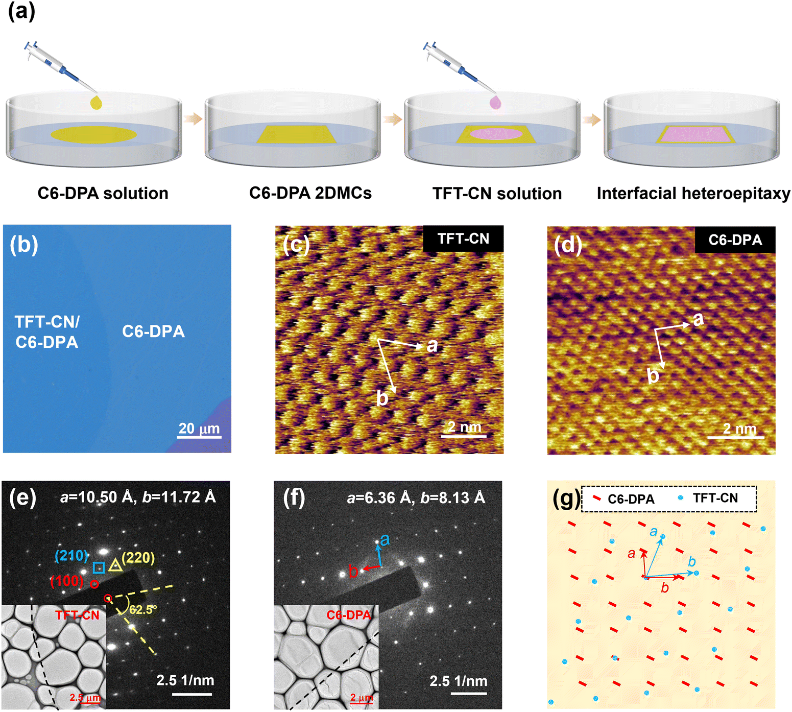 | ||
| Fig. 1 (a) Schematic illustration of the process for growing molecularly thin single-crystalline p–n heterojunctions using an interfacial heteroepitaxy strategy. (b) OM image of the molecularly thin single-crystalline p–n heterojunction. (c) and (d) HR-AFM images of the 2DMCs of TFT-CN and C6-DPA. (e) and (f) SAED patterns of 2DMCs TFT-CN and C6-DPA. Inset: The corresponding TEM images. (g) Schematic diagram showing the lattice relationship in the molecularly thin single-crystalline p–n heterojunctions. | ||
Fig. 1b shows the optical microscopy (OM) image of the p–n heterojunction composed of C6-DPA and TFT-CN 2DMCs. We purposely selected an area showing both the junction part (lefthand) and the 2DMC part (righthand). A clear boundary between the heterojunctions and the substrate is visible, with no cracks on the film surface. The C6-DPA 2DMCs and the heterojunctions exhibit sharp boundaries and distinct color contrasts in the OM image. Polarized optical microscopy (POM) images of the single-crystalline heterojunctions reveal uniform and abrupt color changes as the sample is rotated, indicating the single-crystalline nature of the heterojunctions (Fig. S3, ESI†). The high-resolution atomic force microscopy (HR-AFM) images of TFT-CN and C6-DPA in the p–n heterojunctions are shown in Fig. 1c and d, respectively. The 2D primitive lattice vectors of TFT-CN and C6-DPA are marked by arrows, representing the a-axis and b-axis of each crystal. Fig. 1e and f present bright-field transmission electron microscopy (TEM) images of the 2DMCs TFT-CN and C6-DPA, respectively, along with their corresponding selected area electron diffraction (SAED) patterns. From the TEM images, it can be observed that the surface of the 2DMC exhibits a continuous and smooth morphology with no visible cracks. The dashed boundary (indicated by the black dashed line) highlights a well-defined interface between the 2DMC and the copper grid substrate, confirming that the sample retained its structural integrity during transfer and preparation. These SAED patterns display bright and ordered diffraction spots, demonstrating the crystalline properties of the single components of 2DMCs. Lattice constants for TFT-CN (a = 10.50 Å, b = 11.72 Å, and θ = 62.5°) and C6-DPA (a = 6.36 Å, b = 8.13 Å, and θ = 86.5°), calculated from SAED patterns, were consistent with bulk crystal data.15,36 X-ray diffraction (XRD) patterns of the 2DMCs of C6-DPA, TFT-CN, and their heterojunctions (Fig. S4 ESI†) confirmed the successful preparation of the p–n heterojunctions. Atomic force microscopy (AFM) images of C6-DPA, TFT-CN, and their p–n heterojunctions are shown in Fig. S5a and b, ESI.† The thicknesses of the 2DMCs of C6-DPA and TFT-CN were measured to be 6.33 nm (Fig. S5d, ESI†) and 1.64 nm (Fig. S5c, ESI†), respectively. The single-crystal structures revealed that the layer spacing of TFT-CN and C6-DPA is 1.6 nm and 3.2 nm, respectively, indicating that TFT-CN 2DMC is a monolayer crystal and C6-DPA 2DMC is a bilayer crystal.15,36
Organic single-crystalline p–n heterojunctions with well-defined orientations are essential for polarization detection. Additional HR-AFM images of TFT-CN and C6-DPA in other locations of the p–n heterojunctions are provided in Fig. S6, ESI.† The HR-AFM images confirm that the angle between the b-axis of TFT-CN and the b-axis of C6-DPA in the p–n heterojunction region is approximately 4.6 ± 0.6°, while the angle between the a-axes is approximately 19.7 ± 0.5°. These angles are consistent across all batches of p–n heterojunctions grown by the interfacial heteroepitaxy approach. A schematic of the lattice relationship is shown in Fig. 1g. The lattice mismatch ratio of the b-axis of the TFT-CN crystal and the C6-DPA crystal is approximately 3.2%. This value is larger than those typically observed in inorganic epitaxy. Therefore, the successful production of single-crystalline p–n heterojunctions with defined orientations indicates the high tolerance of organic epitaxy. The photoluminescence (PL) image of C6-DPA and the heterostructure reveals efficient quenching of luminescence in the p–n heterojunction region (Fig. S7, ESI†). The PL spectra (Fig. S8, ESI†) show a significant quenching of the ∼600 nm emission in the heterojunction, which can be attributed to the rapid separation of photogenerated excitons due to the large band offsets for electrons and holes across the heterointerface. This result confirms the expected spontaneous charge transfer at the p–n heterojunctions. Together, these findings confirm the successful fabrication of high-quality, molecularly thin organic single-crystalline p–n heterojunctions with defined orientations.
2.2. Intrinsic anisotropy of molecularly thin single-crystalline p–n heterojunctions with defined orientations
To investigate the anisotropy of the molecularly thin single-crystalline p–n heterojunctions, we performed polarization-resolved absorption spectroscopy (PRAS) and angle-resolved polarized Raman spectroscopy (ARPRS). These techniques provided deeper insights into the anisotropic properties of the heterojunctions. Absorption characteristics in the UV-visible to near-infrared range were observed under parallel (0°) and cross (90°) linearly polarized light. Notably, absorption was greater under 90° (black curve) than under 0° (red curve) across the measured wavelength range (Fig. 2a). A contour map of the PRAS results is shown in Fig. 2b to visualize the anisotropy in optical absorption. Additionally, absorbance values at key wavelengths of 405 nm and 808 nm were extracted and plotted as polar diagrams against the polarization angle to illustrate the angular variation of absorbance, as shown in Fig. 2c. As expected, the angular variation of absorbance follows sinusoidal functions, with the smallest absorbance values observed under parallel polarization and the largest under cross-polarization. The anisotropic absorption ratio as a function of wavelength is provided in Fig. S9 ESI.† | ||
| Fig. 2 (a) Absorption spectra of molecularly thin single-crystalline p–n heterojunctions in the UV-visible to near-infrared range, measured under parallel (0°) and cross (90°) linearly polarized light. (b) Contour map of the polarization-resolved absorption spectroscopy. (c) Polar plots showing the angle dependent absorbance at 405 nm and 808 nm. (d) Raman spectra of C6-DPA, TFT-CN, and their p–n heterojunctions. (e) and (f) Contour color maps of angle-resolved polarized Raman spectra acquired in parallel and cross-polarization configurations. (g) Polar plots of Raman peak intensities at 1401 cm−1 (C6-DPA) and 1435 cm−1 (TFT-CN) under parallel and cross-polarization configurations. | ||
Due to the van der Waals contact between the materials, the overall Raman spectra consist of contributions from both C6-DPA and TFT-CN (Fig. 2d). Contour color maps of Raman peak intensity under parallel and cross-polarization configurations (Fig. 2e and f) show the angular dependence of Raman peak intensity. These results indicate a strong rotational angle dependence of the Raman peaks, highlighting the polarization dependence of the molecularly thin single-crystalline p–n heterojunctions. The Raman characteristic peaks at 1401 cm−1 (C6-DPA) and 1435 cm−1 (TFT-CN) were further studied for angular variation under parallel and cross configurations (Fig. 2g). In the parallel configuration, the Raman peak intensity displays a two-lobed shape, whereas in the cross configuration, it exhibits a four-lobed shape, aligning with typical fitting characteristics.12 ARPRS further revealed that the molecularly thin single-crystalline p–n heterojunctions exhibit highly in-plane anisotropic molecular vibrational properties. The observed intrinsic anisotropy of the heterojunctions underscores their significant potential for applications in polarization detection.
2.3. Photodetection capability of molecularly thin single-crystalline p–n heterojunctions
The optoelectronic properties of the molecularly thin single-crystalline p–n heterojunctions were investigated by fabricating organic field-effect transistors (OFETs) with a top-contact bottom-gate configuration. All measurements were conducted in ambient air at room temperature. Fig. 3a presents a schematic diagram of the molecularly thin single-crystalline p–n heterojunction photodetector. Fig. 3b shows the energy level diagram of C6-DPA and TFT-CN, where their combination forms a type-II heterojunction. Specifically, the type-II band alignment facilitates efficient separation of photogenerated electron–hole pairs, thereby enhancing charge carrier separation efficiency and improving photodetector performance.37,38 The UV-Vis absorption spectra of both the p–n heterojunctions and the single-component 2DMCs demonstrate that the device achieves broadband absorption from the UV-visible to the near-infrared region (Fig. 3c). Fig. 3d illustrates the time-resolved photoresponse of a typical photodetector based on molecularly thin single-crystalline p–n heterojunctions to light signals of varying wavelengths. The device exhibits rapid and stable responses across the wavelength range from 365 to 808 nm, demonstrating broadband detection capability from UV-visible to near-infrared regions and superior photoelectric performance.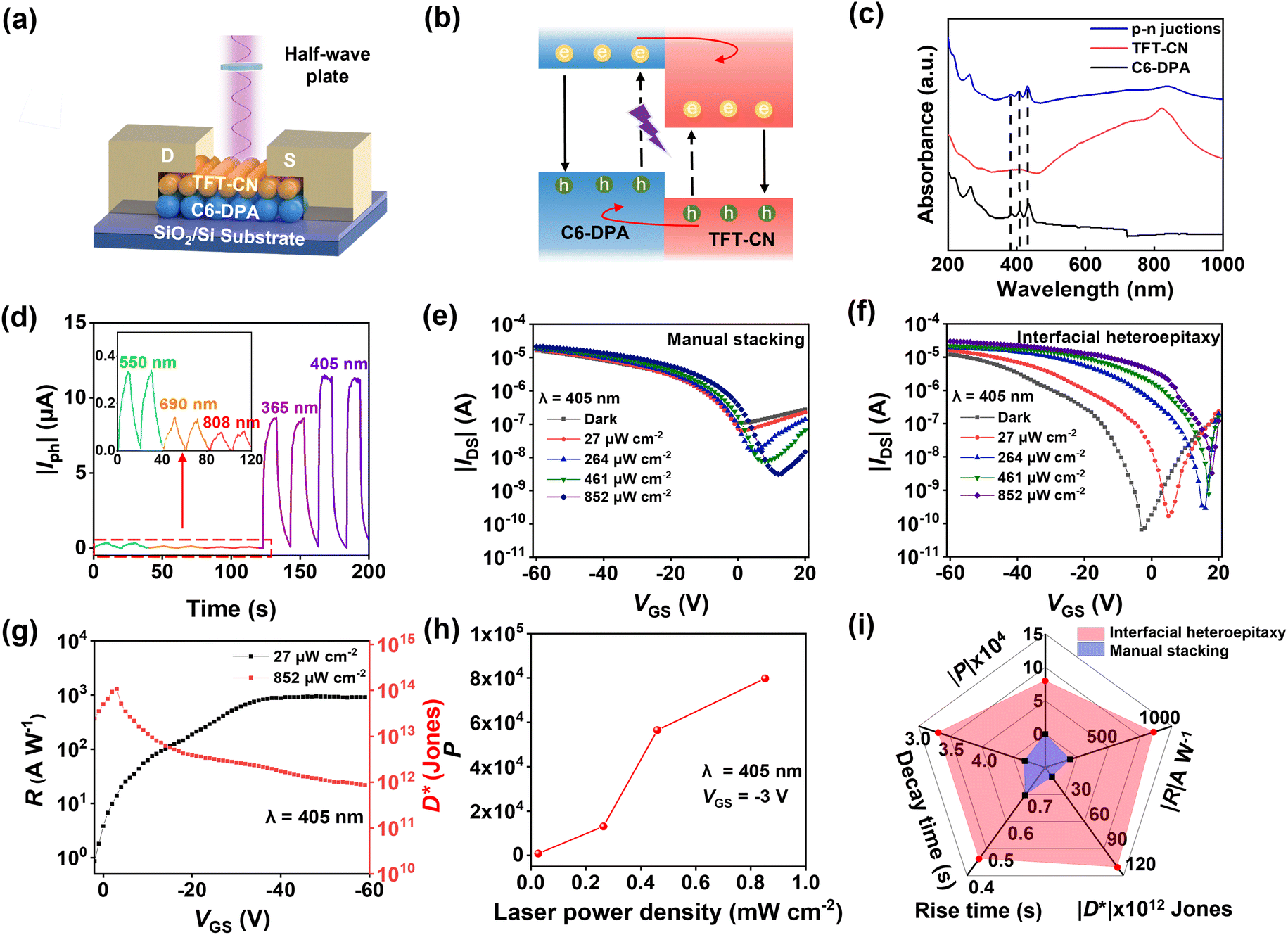 | ||
| Fig. 3 (a) Schematic diagram of the p–n heterojunction photodetector. (b) Energy level diagrams of C6-DPA and TFT-CN, along with the directions of electron transfer in the heterojunctions. (c) UV-Vis absorption spectra of the p–n heterojunctions and single-component 2DMCs. (d) Wavelength-dependent time-resolved photoresponse characteristics. (e) and (f) Transfer curves of organic phototransistors with manual stacking p–n heterojunctions (e) and interfacial heteroepitaxy p–n heterojunctions (f) under dark and varying laser power density conditions. The channel length is 160 μm, and the channel width is 100 μm. (g) R and D* of the molecularly thin single-crystalline p–n heterojunctions photodetector at 405 nm, with varying gate voltages. (h) Relationship between P and laser power density. (i) Radar chart comparing the photodetector performance of molecularly thin single-crystalline p–n heterojunctions and manual stacking p–n heterojunctions. | ||
Key figures of merit, such as photosensitivity (P), responsivity (R), and specific detectivity (D*), are essential for evaluating the performance of photodetectors. P represents the ratio of the photocurrent to the dark current. R represents the ability of the photodetector to convert light signals into noise. Fig. 3e and f show the transfer characteristics of photodetectors based on manual stacking and interfacial heteroepitaxy, respectively. Under 405 nm illumination, as the laser power density increases from 27 μW cm−2 to 852 μW cm−2, the transfer curves shift to positive gate voltages, with both source–drain current and threshold voltage increasing, showing prominent photoresponse. Due to the clean interface of the p–n heterojunctions, the interfacial heteroepitaxy device achieves a dark current of 6.34 × 10⁻¹¹ A, which is four orders of magnitude lower than the manual stacking device (1.19 × 10⁻⁷ A). The calculation formulas of P, R, and D* are presented in the Experimental section. Fig. 3g shows the variation of R and D* with gate voltage (VGS) at 405 nm. As VGS increases, R exhibits a significant rise. At VGS = −50 V and 27 μW cm−2 laser power density, the device achieves a maximum R of 942 A W−1. When shot noise dominates the dark current noise, the maximum D* reaches 1.08 × 10¹⁴ Jones at VGS = −3 V and 852 μW cm−2 laser power density. Fig. 3h illustrates the dependence of P on incident laser power density. As the laser power density increases, P increases significantly. At a laser power density of 852 μW cm−2 and VGS = −3 V, P attains a peak value of 7.98 × 10⁴. It can be calculated from Fig. 3e that the manual stacking device shows poorer performance, with a lower P of 2.79, R of 216 A W−1, and D* of 1.2 × 10¹² Jones. The interfacial heteroepitaxy-based devices demonstrate a four-orders-of-magnitude increase in P, a fourfold increase in R, and a two-orders-of-magnitude increase in D* compared to manually stacked devices.
The photo-switching characteristics at different gate voltages of the heteroepitaxial p–n heterojunctions were studied under a pulsed 405 nm laser at a drain bias of −40 V (Fig. S10 ESI†). To evaluate the stability of the device, we investigated the switching behavior of the p–n heterojunctions (Fig. S11a, ESI†). It was found that the device maintained excellent operational stability over 100 switching cycles, as shown in the enlarged view of the switching cycles in Fig. S11b, ESI,† with no significant degradation in photocurrent or switching speed. The rise (tr) and decay (td) times are the intervals required for the response to rise/decay from 10% to 90% and 90% to 10% of the drain current under light illumination, respectively. The tr/td of the photodetectors based on single-component C6-DPA, manually stacked p–n heterojunctions, and interfacial heteroepitaxy p–n heterojunctions are 0.881/6.591 s, 0.697/4.593 s, and 0.462/3.295 s, respectively. These results demonstrate that the response time of the interfacial heteroepitaxy p–n heterojunction photodetector is significantly faster than that of both the single-component C6-DPA and traditional manually stacked p–n heterojunction photodetector (Fig. S12, ESI†). The molecularly thin single-crystalline p–n heterojunctions exhibit superior overall photodetection performance compared to conventional manual stacking p–n heterojunctions, as displayed in the radar chart (Fig. 3i).
2.4. Polarized light detection capabilities and imaging applications
The polarized photoresponses of the interfacial heteroepitaxy device were investigated under linearly polarized illumination. Fig. 4a and b show the photocurrent response at different polarization angles under 405 nm and 808 nm light irradiation, where the direction of the polarized light changes periodically, resulting in a periodically varying current. The corresponding polar diagrams of polarization photocurrent are presented in Fig. 4c and d. The polarization ratio (PR), calculated from the polar diagrams, is approximately 1.9 at 405 nm and 2.4 at 808 nm, outperforming the manual stacking heterojunctions, which exhibit a typical PR of 1.3 at 405 nm and no significant PR at 808 nm (Fig. S13, ESI†). Fig. 4e and f show the angle-dependent polarized photocurrent mappings of the detector under different VGS during 405 nm and 808 nm light irradiation. By controlling VGS, the PR can increase to 5.19 at 405 nm and 2.47 at 808 nm. The performance metrics of interfacial heteroepitaxy-grown molecularly thin single-crystalline p–n heterojunction devices, such as R, D*, and PR, are comparable to or moderately exceed those of some previously reported organic materials (Table S1, ESI†).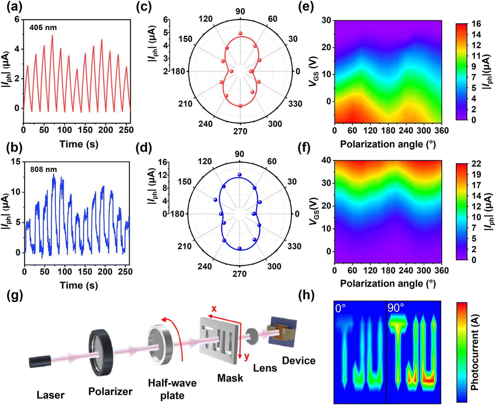 | ||
| Fig. 4 (a) and (b) Photocurrent response at different polarization angles under 405 nm (a) and 808 nm (b) irradiation. (c) and (d) Corresponding polar diagrams of polarized photocurrent under 405 nm (c) and 808 nm (d) irradiation. (e) and (f) Angle-dependent polarized photocurrent mappings of the detector under different gate voltages under 405 nm (e) and 808 nm (f) irradiation. (g) Schematic diagram of the polarization-sensitive imaging system. (h) Polarized photocurrent imaging results of the “TJU” pattern under 405 nm laser irradiation at 0° and 90° polarization angles. | ||
The high performance of the interfacial heteroepitaxy-grown molecularly thin single-crystalline p–n heterojunction devices is attributed to four main factors. First, the high-quality single-crystalline structure with fewer defects is fundamental for efficient charge transport.39–43 Second, the molecularly thin and atomically flat 2DMCs of C6-DPA and TFT-CN ensure low contact resistance.44–46 Third, the highly ordered nature of the 2DMCs and their p–n heterojunctions with well-defined orientations enhances the anisotropy for polarized light detection.12,20,47 Last, the interfacial heteroepitaxy organic single-crystalline p–n heterojunction structure avoids interface contamination and increases photoresponse.
High photoresponsivity, detectivity, and large PR are essential for polarization-sensitive imaging applications. Imaging measurements were performed using a custom-built imaging system (Fig. 4g). The “TJU” pattern was chosen as the imaging target, with a polarizer placed after the signal source to polarize the pattern at 405 nm. The polarization angles of the “TJU” pattern were varied by rotating a half-wave plate. At a polarization angle of 0°, the image appeared blurred, with some edge information missing. At 90°, the image became clear, showing the letter pattern in detail. This improvement in image quality is attributed to the device's high polarization photocurrent ratio, which enables high-contrast imaging (Fig. 4h). These results highlight the potential of molecularly thin single-crystalline p–n heterojunctions for polarization imaging applications.
Although interfacial epitaxy offers significant advantages for growing high-quality heterojunctions, it still faces several key challenges, including limited coverage and poor thickness control in epitaxial growth techniques, as well as high operating voltage. Potential solutions include: (1) delving deeper into how the underlying single crystal's properties impact subsequent layers’ growth, optimizing pre-treatment processes and improving the first layer's quality to enhance coverage and thickness control. (2) exploring the integration of meniscus-guided coating techniques to enable scalable growth and transfer for practical applications. (3) reducing operating voltage by employing gate dielectric materials with high-k dielectric constants and/or reducing dielectric layer thickness.
3. Conclusions
In conclusion, we developed an interfacial heteroepitaxy strategy to fabricate molecularly thin single-crystalline p–n heterojunctions with defined orientations. Compared to traditional manual stacking methods, the heteroepitaxial p–n heterojunction photodetector demonstrates a broadband photoresponse (365–808 nm), with a fast response speed of 0.462 s, a photosensitivity (P) of 7.98 × 10⁴, a responsivity (R) of 942 A W−1 and a specific detectivity (D*) of 1.08 × 10¹⁴ Jones. Moreover, the photodetector exhibits strong polarization sensitivity, with a polarization ratio (PR) of 1.9 at 405 nm and 2.4 at 808 nm. We believe the facile fabrication process and high-quality organic single-crystalline heterojunctions hold great potential for developing high-performance polarization-sensitive photodetectors and integrating them into advanced electronic devices.4. Experimental section
4.1. Materials
C6-DPA and TFT-CN were purchased from Luminescence Technology Corp. All materials were used without purification.4.2. Instrumentation
Optical microscopy (OM) and polarized optical microscopy (POM) images were captured with a Nikon ECLIPSE Ci-POL polarized optical microscope. Transmission electron microscopy (TEM) and selected area electron diffraction (SAED) measurements were performed using a Tecnai G2 F20 S-TWIN transmission electron microscope at a 200 kV accelerating voltage. This work used two types of atomic force microscopy (AFM). Regular AFM was employed to measure the thicknesses of 2DMCs by tapping mode using a Bruker Dimension Icon. High-resolution atomic force microscopy (HR-AFM) was performed in contact mode to measure the molecular arrangements of 2DMCs using an Asylum Cypher S (Oxford Instruments). Fluorescence microscope images were obtained using a Leica DM2700M optical microscope with a plug-in fluorescence unit. UV-vis-NIR absorption spectra were measured with a SHIMADZU UV-3600 Plus spectrophotometer. X-ray diffraction (XRD) was performed on a Rigaku Smartlab diffractometer with monochromatic Cu Kα (λ = 1.541 Å) radiation.4.3. Device fabrication and performance evaluation
In device fabrication, Tungsten probes transfer the pre-deposited Au film onto the crystal surface to make source and drain electrodes, creating a bottom-gate top-contact organic field-effect transistor (OFET) on the SiO2 substrate. To test polarized light response, a Glan-Taylor prism and a half-wave plate are set above the OFET. The prism converts non-polarized into linearly polarized light, and the half-wave plate adjusts its angle. When this linearly polarized light shines on the device's channel region, a Keithley 4200-SCS semiconductor parameter analyzer measures the current at different polarization angles. The R was defined as the ratio of photocurrent (Iph) to the laser power density (W): Iph = Ilight − Idark, R = (Ilight − Idark)/W, where Ilight is the source–drain current under light illumination, and Idark is the dark current. The P reflects the ratio of photocurrent to dark current, calculated as: P = (Ilight − Idark)/Idark. The D* represents the photodetector's ability to detect weak signals. When the shot noise of dark current dominates the noise current, D* is defined as: , where S is the channel area of the device.
Author contributions
R. L. and Z. W. conceived the concept and supervised the work. X. Y. and X. S. conducted most experiments and data analyses. X. T. and J. Y. helped produce the heterojunctions. X. Y., X. S., X. T., and R. L. wrote the manuscript. Y. X. and J. J. helped perform HR-AFM measurements. Y. Y. and Z. W. contributed to the setup of the polarization optical system and the testing of the polarization photocurrents. R. L. and W. H. offered funding acquisition.Data availability
The data supporting this article have been included as part of the ESI.†Conflicts of interest
There are no conflicts to declare.Acknowledgements
The authors acknowledge financial support from the National Key R&D Program of China (grant No. 2024YFA1209600), the National Natural Science Foundation of China (grant No. 52273193 and 52073206), and the Beijing Natural Science Foundation (Z220005). Supported by “the Fundamental Research Funds for the Central Universities.”References
- D. K. Singh, R. Pant, A. M. Chowdhury, B. Roul, K. K. Nanda and S. B. Krupanidhi, ACS Appl. Electron. Mater., 2020, 2, 944–953 Search PubMed.
- D. K. Singh, R. K. Pant, K. K. Nanda and S. B. Krupanidhi, Appl. Phys. Lett., 2021, 119, 121102 Search PubMed.
- D. K. Singh, P. Prajapat, J. Saroha, R. K. Pant, S. N. Sharma, K. K. Nanda, S. B. Krupanidhi and G. Gupta, ACS Appl. Electron. Mater., 2023, 5, 1394–1400 Search PubMed.
- D. Wu, M. Xu, L. Zeng, Z. Shi, Y. Tian, X. J. Li, C.-X. Shan and J. Jie, ACS Nano, 2022, 16, 5545–5555 Search PubMed.
- L. Zeng, Q. Chen, Z. Zhang, D. Wu, H. Yuan, Y. Li, W. Qarony, S. P. Lau, L. Luo and Y. H. Tsang, Adv. Sci., 2019, 6, 1901134 Search PubMed.
- L. Zeng, W. Han, X. Ren, X. Li, D. Wu, S. Liu, H. Wang, S. P. Lau, Y. H. Tsang, C.-X. Shan and J. Jie, Nano Lett., 2023, 23, 8241–8248 Search PubMed.
- L. Tong, X. Huang, P. Wang, L. Ye, M. Peng, L. An, Q. Sun, Y. Zhang, G. Yang, Z. Li, F. Zhong, F. Wang, Y. Wang, M. Motlag, W. Wu, G. J. Cheng and W. Hu, Nat. Commun., 2020, 11, 2308 CrossRef CAS PubMed.
- X. Wang, T. Xiong, K. Zhao, Z. Zhou, K. Xin, H. Deng, J. Kang, J. Yang, Y. Liu and Z. Wei, Adv. Mater., 2022, 34, 2107206 Search PubMed.
- Z. Qin, T. Wang, H. Gao, Y. Li, H. Dong and W. Hu, Adv. Mater., 2023, 35, 2301955 Search PubMed.
- J. Pan, Y. Wu, X. Zhang, J. Chen, J. Wang, S. Cheng, X. Wu, X. Zhang and J. Jie, Nat. Commun., 2022, 13, 6629 Search PubMed.
- Y. Hao, T. Hang, C. Chen, C. Zhang, Y. Chen, C. Yu, S. Wu, J. Yang, Z. Yang, X. Li and G. Cao, Adv. Funct. Mater., 2024, 2416475 Search PubMed.
- T. Wang, K. Zhao, P. Wang, W. Shen, H. Gao, Z. Qin, Y. Wang, C. Li, H. Deng, C. Hu, L. Jiang, H. Dong, Z. Wei, L. Li and W. Hu, Adv. Mater., 2022, 34, 2105665 Search PubMed.
- W. Liu, Y. Yu, M. Peng, Z. Zheng, P. Jian, Y. Wang, Y. Zou, Y. Zhao, F. Wang, F. Wu, C. Chen, J. Dai, P. Wang and W. Hu, InfoMat, 2023, 5, e12470 Search PubMed.
- J. Han, F. Wang, S. Han, W. Deng, X. Du, H. Yu, J. Gou, Q. J. Wang and J. Wang, Adv. Funct. Mater., 2022, 32, 2205150 Search PubMed.
- C. Wang, X. Ren, C. Xu, B. Fu, R. Wang, X. Zhang, R. Li, H. Li, H. Dong, Y. Zhen, S. Lei, L. Jiang and W. Hu, Adv. Mater., 2018, 30, 1706260 Search PubMed.
- J. Wang, H. Wang, X. Yan, H. Huang and D. Yan, Chem. Phys. Lett., 2005, 407, 87–90 Search PubMed.
- J. Wang, H. Wang, X. Yan, H. Huang, D. Jin, J. Shi, Y. Tang and D. Yan, Adv. Funct. Mater., 2006, 16, 824–830 Search PubMed.
- C. Fan, A. P. Zoombelt, H. Jiang, W. Fu, J. Wu, W. Yuan, Y. Wang, H. Li, H. Chen and Z. Bao, Adv. Mater., 2013, 25, 5762–5766 Search PubMed.
- X. Zhang, J. Mao, W. Deng, X. Xu, L. Huang, X. Zhang, S.-T. Lee and J. Jie, Adv. Mater., 2018, 30, 1800187 Search PubMed.
- S. Chen, X. Ma, Z. Cai, H. Long, X. Wang, Z. Li, Z. Qu, F. Zhang, Y. Qiao and Y. Song, Adv. Mater., 2022, 34, 2200928 Search PubMed.
- S. Duan, T. Wang, B. Geng, X. Gao, C. Li, J. Zhang, Y. Xi, X. Zhang, X. Ren and W. Hu, Adv. Mater., 2020, 32, 1908388 Search PubMed.
- Z. Chen, S. Duan, X. Zhang, B. Geng, Y. Xiao, J. Jie, H. Dong, L. Li and W. Hu, Adv. Mater., 2022, 34, 2104166 CrossRef CAS PubMed.
- W. Deng, H. Lei, X. Zhang, F. Sheng, J. Shi, X. Zhang, X. Liu, S. Grigorian, X. Zhang and J. Jie, Adv. Mater., 2022, 34, 2109818 CrossRef CAS PubMed.
- X. Liu, Y. Zhang, X. Zhang, R. Li and W. Hu, Sci. China Mater., 2020, 63, 1257–1264 Search PubMed.
- B. Fu, F. Yang, L. Sun, Q. Zhao, D. Ji, Y. Sun, X. Zhang and W. Hu, Adv. Mater., 2022, 34, 2203330 Search PubMed.
- S. Yang, Y. Zhang, Y. Wang, J. Yao, L. Zhang, X. Ren, X. Li, S. Lei, X. Zhang, F. Yang, R. Li and W. Hu, Chem. Commun., 2021, 57, 2669–2672 Search PubMed.
- C. Xu, P. He, J. Liu, A. Cui, H. Dong, Y. Zhen, W. Chen and W. Hu, Angew. Chem., Int. Ed., 2016, 55, 9519–9523 CrossRef CAS PubMed.
- Q. Wang, F. Yang, Y. Zhang, M. Chen, X. Zhang, S. Lei, R. Li and W. Hu, J. Am. Chem. Soc., 2018, 140, 5339–5342 CrossRef CAS PubMed.
- X. Tian, J. Yao, L. Zhang, B. Han, J. Shi, J. Su, J. Liu, C. Li, X. Liu, T. Zhai, L. Jiang, F. Yang, X. Zhang, Y. Zou, R. Li and W. Hu, Nano Res., 2022, 15, 2667–2673 Search PubMed.
- S. Guo, J. Yao, Y. Wang, L. Zhang, F. Zhai, X. Zhang, Y. Feng, W. Feng, X. Zhang, J. Jie, F. Yang, R. Li and W. Hu, J. Mater. Chem. C, 2021, 9, 5758–5764 Search PubMed.
- L. Zhang, X. Tian, J. Yao, X. Song, S. Yang, S. Guo, Y. Wang, B. Li, X. Ren, Y. Sun, F. Yang, R. Li and W. Hu, J. Mater. Chem. C, 2021, 9, 8834–8841 Search PubMed.
- X. Tian, J. Yao, S. Guo, Z. Wang, Y. Xiao, H. Zhang, Y. Feng, W. Feng, J. Jie, F. Yang, R. Li and W. Hu, J. Mater. Chem. C, 2022, 10, 2575–2580 Search PubMed.
- X. Zhu, Y. Zhang, X. Ren, J. Yao, S. Guo, L. Zhang, D. Wang, G. Wang, X. Zhang, R. Li and W. Hu, Small, 2019, 15, 1902187 Search PubMed.
- J. Yao, X. Tian, S. Yang, F. Yang, R. Li and W. Hu, APL Mater., 2021, 9, 051108 CrossRef CAS.
- C. Xu, P. He, J. Liu, A. Cui, H. Dong, Y. Zhen, W. Chen and W. Hu, Angew. Chem., Int. Ed., 2016, 55, 9519–9523 CrossRef CAS PubMed.
- J. Yao, Y. Zhang, X. Tian, X. Zhang, H. Zhao, X. Zhang, J. Jie, X. Wang, R. Li and W. Hu, Angew. Chem., Int. Ed., 2019, 58, 16082–16086 Search PubMed.
- W. Zhang, K.-H. Chiao, H.-W. Huang, M. Abid, C. Ó. Coileáin, K.-M. Hung, C.-R. Chang, Y.-R. Wu and H.-C. Wu, ACS Appl. Mater. Interfaces, 2025, 17, 12941–12951 CrossRef PubMed.
- D. K. Singh, B. Roul, R. Pant, A. M. Chowdhury, K. K. Nanda and S. B. Krupanidhi, Appl. Phys. Lett., 2020, 116, 252102 CrossRef CAS.
- F. Yang, S. Cheng, X. Zhang, X. Ren, R. Li, H. Dong and W. Hu, Adv. Mater., 2018, 30, 1702415 CrossRef PubMed.
- Y. Xie, C. Ding, Q. Jin, L. Zheng, Y. Xu, H. Xiao, M. Cheng, Y. Zhang, G. Yang, M. Li, L. Li and M. Liu, SmartMat, 2024, 5, e1261 Search PubMed.
- F. Yang, L. Sun, Q. Duan, H. Dong, Z. Jing, Y. Yang, R. Li, X. Zhang, W. Hu and L. Chua, SmartMat, 2021, 2, 99–108 Search PubMed.
- X. Tian, J. Yao, R. Li and W. Hu, Sci. Sin. Chim., 2021, 51, 21–40 CrossRef.
- M. Chen, B. Peng, R. A. Sporea, V. Podzorov and P. K. L. Chan, Small Sci., 2022, 2, 2100115 Search PubMed.
- Y. Zhang, J. Qiao, S. Gao, F. Hu, D. He, B. Wu, Z. Yang, B. Xu, Y. Li, Y. Shi, W. Ji, P. Wang, X. Wang, M. Xiao, H. Xu, J.-B. Xu and X. Wang, Phys. Rev. Lett., 2016, 116, 016602 Search PubMed.
- J. J. Brondijk, W. S. C. Roelofs, S. G. J. Mathijssen, A. Shehu, T. Cramer, F. Biscarini, P. W. M. Blom and D. M. De Leeuw, Phys. Rev. Lett., 2012, 109, 056601 CrossRef CAS PubMed.
- H. Jiang, K. J. Tan, K. K. Zhang, X. Chen and C. Kloc, J. Mater. Chem., 2011, 21, 4771 RSC.
- M. Dong, Y. Zhang, J. Zhu, X. Zhu, J. Zhao, Q. Zhao, L. Sun, Y. Sun, F. Yang and W. Hu, Adv. Mater., 2024, 36, 2409550 Search PubMed.
Footnotes |
| † Electronic supplementary information (ESI) available. See DOI: https://doi.org/10.1039/d5tc00456j |
| ‡ These authors contributed equally to this work. |
| This journal is © The Royal Society of Chemistry 2025 |