
 Open Access Article
 This Open Access Article is licensed under a
 Creative Commons Attribution 3.0 Unported Licence
Achieving clear ferroelectric polarization reversal in room-temperature multiferroic ε-Fe2O3 systems through grain boundary engineering†
Tsukasa
Katayama
 *ab,
Shintaro
Yasui
*c,
Takahisa
Shiraishi
de,
Takanori
Kiguchi
de,
Badari Narayana
Rao
f,
Yosuke
Hamasaki
g and
Mitsuru
Itoh
*fh
*ab,
Shintaro
Yasui
*c,
Takahisa
Shiraishi
de,
Takanori
Kiguchi
de,
Badari Narayana
Rao
f,
Yosuke
Hamasaki
g and
Mitsuru
Itoh
*fh
aResearch Institute for Electronic Science, Hokkaido University, N20W10, Kita, Sapporo 001-0020, Japan
bJST-PRESTO, Kawaguchi, Saitama 332-0012, Japan. E-mail: katayama@es.hokudai.ac.jp
cLaboratory for Zero-Carbon Energy, Institute of Science Tokyo, 2-12-1, Ookayama, Meguro-ku, Tokyo 152-8550, Japan. E-mail: yasui.s.aa@m.titech.ac.jp
dDepartment of Materials Science, Graduate School of Science and Technology, Kumamoto University, 2-39-1 Kurokami, Chuo-ku, Kumamoto 860-8555, Japan
eMagnesium Research Center, Kumamoto University, 2-39-1 Kurokami, Chuo-ku, Kumamoto 860-8555, Japan
fLaboratory for Materials and Structures, Institute of Science Tokyo, 4259, Nagatsuta-cho, Midori-ku, Yokohama 226-8501, Japan. E-mail: mitsuru_itoh@icloud.com
gDepartment of Applied Physics, National Defense Academy, Yokosuka 239-8686, Japan
hEnvironmental Safety Center, Institute of Science Tokyo, 4259 Nagatsuta-cho, Midori-ku, Yokohama 226-8501, Japan
First published on 19th May 2025
Abstract
ε-Fe2O3-related oxides are promising room-temperature multiferroic materials owing to their significant magnetization and switchable ferroelectric polarization. However, their large leakage current hinders the quality of ferroelectric polarization reversal, limiting research despite superior magnetic properties compared to the well-studied BiFeO3 system. This study addresses these limitations through two investigations. First, we investigate the difficulty of polarization reversal by analyzing grain boundary structures in ε-Fe2O3-related epitaxial films, which inherently form due to their non-perovskite orthorhombic structure. Second, we enhance polarization reversal via grain boundary engineering. Our findings reveal that these films contain numerous small grains (250–770 nm2) with Fe2+/3+ states at grain boundaries, where approximately 40% act as ferroelectric domain walls. The high grain boundary density causes significant leakage current and hinders polarization reversal. By implementing a codoping method, we successfully reduce the grain boundary density, achieving clear ferroelectric hysteresis. This breakthrough highlights the potential of ε-Fe2O3-related oxides as room-temperature multiferroic materials with substantial magnetization and offers new prospects for research on materials distinct from the BiFeO3 system.
1. Introduction
Multiferroic materials are a fascinating class of materials that exhibit both ferroelectric and ferromagnetic properties within a single phase. This dual nature has the potential to advance fundamental physics and enable innovative applications, such as rapid data writing, energy-efficient devices, and secure data storage, and hence, multiferroic materials have attracted considerable interest.1,2 However, the coexistence of ferroelectric and magnetic behavior at room temperature remains rare. Two categories of room-temperature multiferroic materials have been identified: oxide materials related to BiFeO33–9 and ε-Fe2O3.10–25 Materials in these two categories differ substantially in their crystal structures as well as their intrinsic properties.The BiFeO3-related oxides with a perovskite structure are distinguished by their ability to achieve clear ferroelectric polarization (P) reversal under an applied electric field (E). These materials exhibit excellent piezoelectric properties, with a remanent polarization (Pr) of approximately 60 μC cm−2 and a piezoelectric coefficient (d33) of 70 pm V−1.3,4 The coupling between the magnetic moment direction and polarization direction in BiFeO3 allows for the modification of the magnetic moment orientation via E-induced polarization reversal at room temperature.5–7 However, as BiFeO3 exhibits antiferromagnetic ordering, the remanent magnetization (Mr) is nearly zero.8 Although the spin structure can be tuned by substrate-induced strain or chemical substitution (e.g., Co doping), the Mr value is still limited.9
In contrast, ε-Fe2O3-related oxides exhibit substantial magnetization and coercive force at room temperature due to their ferrimagnetic nature.10–14 For instance, Rh doping leads to a remarkable coercive force of 24 kOe, the highest value among oxide magnets, and Ga doping increases Mr to 0.6μB f.u.−1 at 300 K.10 These oxides have been investigated for applications related to their magnetic properties, including photo-induced magnetization reversal memory11 and millimeter-wave absorption.12,13 Moreover, E-induced polarization reversal has been demonstrated in thin-film ε-Fe2O3-related oxides at room temperature.15–25 However, the reported P–E hysteresis loops indicate significant leakage currents, which hinder the quality of ferroelectric polarization reversal. ε-Fe2O3-related oxides have not been extensively investigated in the field of multiferroics because they exhibit relatively poor polarization reversal properties in comparison to BiFeO3. Nonetheless, given the excellent magnetic properties of ε-Fe2O3-related oxides, establishing clear design guidelines for achieving reliable electric-field-induced ferroelectric polarization reversal can help significantly improve their multiferroic application prospects.
The reason for the difficulty in achieving ferroelectric polarization reversal in ε-Fe2O3-related oxides remains unclear. The challenge is attributed primarily to their unique crystal structure, which deviates from the common perovskite structure of BiFeO3. The crystal structure of ε-Fe2O3 comprises octahedral (Oh) FeA, FeB, and FeC sites, as well as tetrahedral (Td) FeD sites (Fig. 1(a)). The presence of grain boundaries (GBs) in the films further complicates the issue: thin films reported in the literature consist of three types of in-plane grains with the polar axis (c-axis) oriented along the out-of-plane direction (Fig. 1(b)).
 | ||
| Fig. 1 (a) Crystal structures of ε-Fe2O3 and (b) top-view schematic of the ε-Fe2O3-related oxide film grown on the STO(111) substrate. (c) 2θ–θ X-ray diffraction pattern and (d) ϕ-scan of the Ga-doped ε-Fe2O3 film. | ||
This study has two key objectives. First, we aim to elucidate the grain boundary structure and identify the factors hindering polarization reversal. Second, we explore grain boundary engineering as a strategy to achieve clear ferroelectric polarization reversal. We investigate the grain structures via plan-view and cross-sectional transmission electron microscopy (TEM) and high-angle annular dark-field scanning TEM (HAADF-STEM) measurements on three types of ε-Fe2O3-related oxide films: Ga0.8Fe1.2O3, Sc0.5Fe1.5O3, and Ga0.4Sc0.2Fe1.4O3. Hereafter, these films are referred to as Ga-doped, Sc-doped, and (Ga,Sc)-codoped ε-Fe2O3 films, respectively.
Our findings revealed that the films contained significantly small grains, with the average sizes ranging from 250 to 770 nm2. Fe2+/3+ states were present at the GBs, and approximately 40% of the GBs corresponded to ferroelectric domain walls. This high density of GBs was identified as the primary source of the large leakage current and the reason for the difficulty in achieving polarization reversal. Furthermore, Ga and Sc codoping reduced the density of GBs, enabling clear ferroelectric polarization reversal in the films.
2. Results and discussion
2.1. Domain wall structure characteristics
Fig. 1(c) illustrates the 2θ–θ X-ray diffraction (XRD) patterns of the Ga-doped ε-Fe2O3 film. The 002, 004, and 006 XRD peaks were clearly observed, indicating that a c-axis-oriented film with an ε-Fe2O3 structure was obtained. As illustrated in the ϕ-scan results (Fig. 1(d)), the film exhibited sixfold in-plane symmetry, whereas the STO(111) plane exhibited threefold symmetry. Considering the orthorhombic structure of ε-Fe2O3, the film consisted of three types of in-plane grains, G1, G2, and G3, which were rotated by 120° relative to each other as illustrated in Fig. 1(b).Fig. 2(a) illustrates a plan-view TEM image of the Ga-doped ε-Fe2O3 film. Stripe-like patterns were observed. Compared with the FeB and FeC sites (blue and light blue circles in Fig. 1(a)), the FeA and FeD sites (orange and green points) are expected to be more clearly observed in the plan-view TEM image because they overlap along the out-of-plane direction. Thus, the stripe-like patterns were derived from the zigzag lines of the FeA and FeD atoms, which correspond to the orange and green lines in Fig. 1. The direction of the grains in the plan-view TEM image was determined based on the direction of the stripe-like patterns. The G1, G2, and G3 grain types are colored red, green, and blue, respectively, in Fig. 2(a). Fig. 2(b) illustrates a histogram of the grain size. The average size was as small as 250 nm2. These small grains formed a nanomosaic-like pattern in the film.
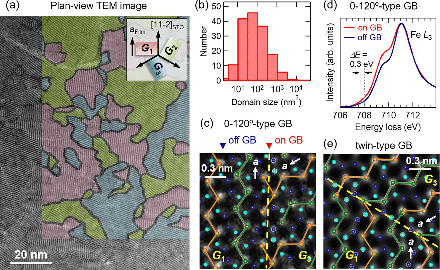 | ||
| Fig. 2 (a) Plan-view TEM image. (b) A histogram of the grain size. (c) Plan-view STEM image and (d) on- and off-GB Fe L3-edge EELS spectra near the 0–120°-type grain boundaries (GBs). (e) Plan-view STEM image near twin-type GBs for the Ga-doped ε-Fe2O3 film. | ||
The GB structure was investigated via HAADF-STEM measurements. Typical GB structures were 0–120°-type and twin-type, as illustrated in Fig. 2(c) and (e), respectively. The 0–120°-type GB was formed by the connection between a (100) grain and a (110) grain. This connection is preferred because the a-axis length (5.06 Å) matches well with the value of  (5.06 Å). In the twin-type GB, the mirror plane was formed in the direction parallel to the (110) plane, which crossed all cation sites. Although ε-Fe2O3 exhibits spontaneous polarization along the c-axis, and thus no intrinsic in-plane polarization is expected, the formation of twin-type grain boundaries could induce strain that may locally generate in-plane polarization components. Further investigation is required to clarify this possibility.
Fig. 2(d) and Fig. S1 (ESI†) illustrate the Fe L-edge electron energy loss spectroscopy (EELS) plots for the 0–120°-type GB (on-GB) and within the grain (off-GB). Both spectra exhibited prominent and left-shoulder peaks at 711 and 709.5 eV, respectively. The intensity of the shoulder peak in the on-GB spectrum was higher than that in the off-GB spectrum, indicating the reduced valence state of the Fe ions in the GB. The difference in the starting energy of the peak (ΔE) between the on- and off-GB regions was 0.3 eV. Thus, the valence state of the Fe ions in the GB is expected to be ∼2.8+.26 This implies that oxygen vacancies were generated in the GB.
The GB structure was also investigated via cross-sectional HAADF-STEM measurements. In the HAADF-STEM measurements, the electron beam was irradiated in the [11−2]STO direction (Fig. 3(a)). Fig. 3(b) shows the cross-sectional images of ε-Fe2O3 in the G1 and G3 domains. The atomic arrangement, marked in yellow boxes, can be used to determine the polarization direction. For example, when ε-Fe2O3 exhibits an upward polarization (up-P) in the G1 domain, the positions of the four atoms in the yellow box change to down-up-up-down. Meanwhile, in the up-P G3 domain, the three atoms in the yellow box have an up-down-up arrangement.
 | ||
| Fig. 3 (a) Top-view and (b) cross-sectional images of ε-Fe2O3. (c) and (d) Cross-sectional HAADF-STEM images of the Ga-doped ε-Fe2O3 film. | ||
Fig. 3(c) illustrates a cross-sectional HAADF-STEM image of the region near the GB. Based on the atomic arrangement, the left and right domains were identified as up-P G1 and up-P G3, respectively. We also observed GBs between the domains with opposite P directions (Fig. 3(d)). We observed 12 GBs in the Ga-doped ε-Fe2O3 film and found that five of them were formed between grains with opposite P directions. This suggests that approximately 40% of the GBs are ferroelectric 180°-domain walls (FE DWs). ε-Fe2O3 has four layers along the c-axis (Fig. 4(a)): L1 and L3 layers consisting of FeA and FeD sites and L2 and L4 layers consisting of FeB and FeC sites. The L1 layer of one grain was connected to either the L1 or L3 layer of another grain in all the observed GBs.
 | ||
| Fig. 4 (a) P-reversal mechanism in ε-Fe2O3. (b) 0–120°-type GB structure between the up-P G1 and up-P G3 domains. (c) Expected GB structure after P reversal in the G1 domain. | ||
2.2. The origin of the difficulty in obtaining clear ferroelectric reversal
We identified the 0–120°-type GB structure from the plan-view and cross-sectional STEM measurements. Fig. 4(b) illustrates the 0–120°-type GBs between the up-P G1 and up-P G3 grains. New cationic arrangements, such as FeD-site tetrahedron trimers, were observed in the GB. ε-Fe2O3 is known to have a unique P-reversal mechanism.16,17 During P reversal, the octahedral (Oh) FeA and tetrahedral (Td) FeD sites in the L1 and L3 layers were switched, while FeB and FeC sites in the L2 and L4 layers were shifted along the a-axis (Fig. 4(a)). Fig. 4(c) illustrates the expected GB structure after P reversal in the G1 domain. Pyramidal FeO5 appeared in the GB in the L1 and L3 layers after P reversal. In addition, the connection between the FeB and FeC sites was slightly distorted in the L2 and L4 layers. Thus, the activation energy for P reversal increased near the GB; in other words, P reversal was restricted by the GBs in the film. X. Guan et al. conducted in situ STEM observations while applying an electric field to ε-Fe2O3 films and reported that ferroelectric switching tends to occur more readily near ferroelectric domain walls within a single grain.27 This finding supports the idea that reducing the density of grain boundaries—which inhibit ferroelectric switching—and increasing grain size are crucial for improving ferroelectric properties.2.3. Achieving clear ferroelectric reversal via domain engineering
Obtaining a good ferroelectric hysteresis loop in ε-Fe2O3-related oxides is challenging. We found that this difficulty is due to the high density of GBs with Fe2+/3+ states, which inhibits P reversal, as shown in Fig. 4. Therefore, we attempted to increase the grain size through chemical substitution. Fig. 5(a)–(e) and Fig. S2 (ESI†) illustrate the plan-view TEM images and histograms of the grain size for the Ga-doped, Sc-doped, and Ga,Sc-codoped ε-Fe2O3 films. The average grain size of the Ga,Sc-codoped film (770 nm2, Fig. 5(e)) was three times larger than that of the Ga-doped film (250 nm2, Fig. 5(c)). This may be attributed to two reasons. First, new cationic arrangements, such as FeD-site tetrahedron trimers, are formed at the GBs. However, such cationic arrangements may be unstable depending on the elemental species, which, in turn, may increase the energy required for GB formation. Second, the difference between the a-axis length and value leads to strain near the GBs and results in an increase in the energy required for GB formation. Further investigation is necessary to elucidate the reasons in detail.
 | ||
| Fig. 5 Plan-view TEM images and histograms of the grain size for the (a) and (c) Ga-doped, (d) Sc-doped, and (b) and (e) Ga,Sc-codoped ε-Fe2O3 films. (f) Leakage current and (g) permittivity of the films at 300 K. | ||
Fig. 5(f) illustrates the leakage current (I) for the films at ±500 kV cm−1. The I value decreases with increasing grain size, reflecting the reduction in the number of the GBs with Fe2+/3+ state. Fig. 5(g) illustrates the frequency dependence of the dielectric constants (ε′) of the films. The films exhibit relaxation frequencies of 10–50 kHz due to dielectric relaxation through oxygen vacancies, which are coupled with the Fe2+ ions.21ε′ tends to decrease, particularly below the relaxation frequency, with an increase in the grain size because of the reduction in the number of oxygen vacancies that are located at the GBs.
Fig. 6(a) illustrates the P versus electric field (P–E) hysteresis loops for the Sc-doped and Ga,Sc-codoped ε-Fe2O3 films at 300 K. The Ga-doped film did not exhibit ferroelectric behavior in the P–E curve because of the high density of GBs, as discussed in Section 2.2. In contrast, the Sc- and Ga,Sc-codoped films exhibited clear ferroelectric hysteresis loops with minimal leakage currents in the P–E curves. The remanent polarizations (Pr) of the Sc-doped and Ga,Sc-codoped films were 3.5 and 4.5 μC cm−2, respectively. The obtained Pr values were smaller than the calculated values for GaFeO3-type Fe2O3 (21 μC cm−2) and GaFeO3 (25 μC cm−2).16,17,28 The decrease in Pr with decreasing grain size is also observed in ferroelectric Pb(ZrxTi1−x)O3.29 This is attributed primarily to the pinning of ferroelectric domains at the GBs due to the high activation energy of polarization reversal at the GBs. Thus, a strong relationship between the ferroelectric properties and GBs exists in ε-Fe2O3-related oxide films, and increasing the grain size is key to improving their ferroelectric properties. The Sc-doped and Ga,Sc-codoped films also exhibited ferrimagnetic properties at 300 K (Fig. 6(b)), confirming the coexistence of spontaneous polarization and magnetization at room temperature.
 | ||
| Fig. 6 (a) Polarization (P) versus electric field (E) and (b) magnetization (M) versus magnetic field (H) curves for the Sc-doped and Ga,Sc-codoped ε-Fe2O3 films at 300 K. | ||
3. Conclusion
The GB structures of room-temperature multiferroic ε-Fe2O3-related oxide films were investigated via plan-view and cross-sectional TEM and STEM measurements. The grain sizes of the films were as small as 250–770 nm2. The STEM-EELS measurements revealed that the valence state of Fe was reduced at the GBs. Cross-sectional STEM measurements indicated that approximately 40% of the GBs were FE DWs. The large leakage current and the difficulty in achieving good P reversal behavior in ε-Fe2O3-related oxide films were attributed to the high density of GBs. Therefore, we reduced the density of GBs via codoping and achieved clear ferroelectric hysteresis with minimal leakage current. The results obtained in this study are expected to catalyze further research on room-temperature multiferroic materials with large magnetization distinct from the BiFeO3 system.4. Experimental
The Ga-doped, Sc-doped, and Ga,Sc-codoped ε-Fe2O3 films were fabricated on SrTiO3(111) (STO) and Nb 0.5 wt%-doped STO(111) substrates via pulsed laser deposition. The chemical compositions of the films were Ga0.8Fe1.2O3, Sc0.5Fe1.5O3, and Ga0.4Sc0.2FeO3, respectively. The substrate temperature and oxygen partial pressure during the deposition were maintained at 700 °C and 200 mTorr, respectively. The fourth harmonic of an Nd:YAG pulsed laser (wavelength: 266 nm) was used with an energy of 12 mJ per pulse and a repetition rate of 5 Hz. The laser spot size was approximately 1 mm2, and the distance between the target and the substrate was 50 mm. The typical thickness of the films was 30–40 nm.The crystal structures of the films were determined via high-resolution XRD with Cu-Kα1 radiation (Rigaku Smartlab). The microstructure was investigated via TEM and HAADF-STEM measurements using a JEM-ARM200F cold FEG instrument. In our EELS measurements, the acquisition points were manually selected by observing the STEM image in real time, as our system does not include an automated protocol for positioning EELS measurements. We performed the EELS measurements several times, and during the process, we observed instances of apparent chemical shifts. However, we only used data sets that showed minimal chemical shift and in which the EELS acquisition point clearly coincided with the grain boundary location in the STEM image. The leakage current was measured via the conventional two-probe method (Keithley 2450 SourceMeter) at room temperature. We did not use the step relaxation method for the leakage current measurements. Instead, the current–voltage (I–V) characteristics were measured by applying a voltage in steps of 0.1 seconds per voltage point. The dielectric properties were measured using a precision LCR meter (Agilent, 4284A) at room temperature. The ferroelectric properties were investigated using a ferroelectric tester (Toyo Corporation FCE-1E) at room temperature. The ferroelectric hysteresis loops were performed at a frequency of 10 kHz. Pt electrodes and Nb:STO substrates were respectively used as the top and bottom electrodes while measuring the leakage current, dielectric properties, and ferroelectric properties. The diameter of the Pt electrodes used for the ferroelectric and leakage current measurements was 100 μm, and that of the Pt electrodes used for the dielectric measurements was 200 μm. The magnetization of the films was measured using a superconducting quantum interference device magnetometer (Quantum Design, MPMS XL).
Data availability
All data supporting the findings of this study are included in the main manuscript.Conflicts of interest
There are no conflicts to declare.Acknowledgements
This study was partially supported by JST PRESTO (JPMJPR21Q3), JST A-STEP (JPMJTR24032140), JSPS KAKENHI Grants-in-Aid (22H01768), and Tohoku univ. CINTS (A-18-TU-0013, A-17-TU-0009, A-16-TU-0038).References
- T. Kimura, T. Goto, H. Shintani, K. Ishizaka, T. Arima and Y. Tokura, Magnetic control of ferroelectric polarization, Nature, 2003, 426, 55 CrossRef CAS PubMed.
- J. F. Scott, Multiferroic memories, Nat. Mater., 2007, 6, 256 CrossRef CAS PubMed.
- J. Wang, et al., Epitaxial BiFeO3 Multiferroic Thin Film Heterostructures, Science, 2003, 299, 5613 Search PubMed.
- D. Lebeugle, et al., Room-temperature coexistence of large electric polarization and magnetic order in BiFeO3 single crystals, Phys. Rev. B: Condens. Matter Mater. Phys., 2007, 76, 024116 CrossRef.
- K. Shimizu, et al., Direct Observation of Magnetization Reversal by Electric Field at Room Temperature in Co-Substituted Bismuth Ferrite Thin Film, Nano Lett., 2019, 19, 1767 CrossRef CAS PubMed.
- N. Waterfield Price, et al., Electrical Switching of Magnetic Polarity in a Multiferroic BiFeO3 Device at Room Temperature, Phys. Rev. Appl., 2017, 8, 014033 CrossRef.
- P. Meisenheimer, et al., Switching the spin cycloid in BiFeO3 with an electric field, Nat. Commun., 2024, 15, 2903 CrossRef CAS PubMed.
- H. Béa, et al., Influence of parasitic phases on the properties of BiFeO3 epitaxial thin films, Appl. Phys. Lett., 2005, 87, 072508 CrossRef.
- M. Azuma, H. Hojo, K. Oka, H. Yamamoto, K. Shimizu, K. Shigematsu and Y. Sakai, Functional Transition Metal Perovskite Oxides with 6s2 Lone Pair Activity Stabilized by High-Pressure Synthesis., Annu. Rev. Mater. Res., 2021, 51, 329–349 CrossRef CAS.
- A. Namai, M. Yoshikiyo, K. Yamada, S. Sakurai, T. Goto, T. Yoshida, T. Miyazaki, M. Nakajima, T. Suemoto, H. Tokoro and S. Ohkoshi, Hard magnetic ferrite with a gigantic coercivity and high frequency millimetre wave rotation, Nat. Commun., 2012, 3, 1035 CrossRef PubMed.
- S. Ohkoshi, K. Imoto, A. Namai, M. Yoshikiyo, S. Miyashita, H. Qiu, S. Kimoto, K. Kato and M. Nakajima, Rapid Faraday Rotation on ε-Iron Oxide Magnetic Nanoparticles by Visible and Terahertz Pulsed Light, J. Am. Chem. Soc., 2019, 141(4), 1775–1780 CrossRef CAS PubMed.
- S. Ohkoshi, S. Kuroki, S. Sakurai, K. Matsumoto, K. Sato and S. Sasaki, A millimeter-wave absorber based on gallium-substituted ε-iron oxide nanomagnets, Angew. Chem., Int. Ed., 2007, 46, 8392–8395 CrossRef CAS PubMed.
- S. Tsukamoto, Y. Oki, K. Imoto, A. Namai, M. Yoshikiyo and S. Ohkoshi, Resonance Frequency Tuning of a 200
![[thin space (1/6-em)]](https://www.rsc.org/images/entities/char_2009.gif) GHz Band Absorber by an External Magnetic Field, Adv. Photonics Res., 2022, 3, 2100319 CrossRef CAS.
GHz Band Absorber by an External Magnetic Field, Adv. Photonics Res., 2022, 3, 2100319 CrossRef CAS. - J. Jin, S. Ohkoshi and K. Hashimoto, Giant coercive field of nanometer-sized iron oxide, Adv. Mater., 2004, 16, 48 CrossRef CAS.
- S. Mukherjee, A. Roy, S. Auluck, R. Prasad, R. Gupta and A. Garg, Room temperature nanoscale ferroelectricity in magnetoelectric GaFeO3 epitaxial thin films, Phys. Rev. Lett., 2013, 111, 087601 CrossRef PubMed.
- K. Xu, J. S. Feng, Z. P. Liu and H. J. Xiang, Origin of ferrimagnetism and ferroelectricity in room-temperature multiferroic ε-Fe2O3, Phys. Rev. Appl., 2018, 9, 044011 CrossRef CAS.
- B. N. Rao, A. Yasui, T. Katayama, A. Taguchi, H. Moriwake, Y. Hamasaki and M. Itoh, Investigation of ferrimagnetism and ferroelectricity in AlxFe2−xO3 thin films, J. Mater. Chem. C, 2020, 8, 706 RSC.
- H. Wang, Y. Zhang, K. Tachiyama, Z. Xia, J. Fang, Q. Li, G. Cheng, Y. Shi, J. Yu, T. Katayama, S. Yasui and M. Itoh, Large Polarization Switching and High-Temperature Magnetoelectric Coupling in Multiferroic GaFeO3 Systems, Inorg. Chem., 2021, 60, 225 CrossRef CAS PubMed.
- M. Gich, I. Fina, A. Morelli, F. Sánchez, M. Alexe, J. Gàzquez, J. Fontcuberta and A. Roig, Multiferroic iron oxide thin films at room temperature, Adv. Mater., 2014, 26, 4645 CrossRef CAS PubMed.
- S. Song, H. M. Jang, N. Lee, J. Y. Son, R. Gupta, A. Garg, J. Ratanapreechachai and J. F. Scott, Ferroelectric polarization switching with a remarkably high activation energy in orthorhombic GaFeO3 thin films, NPG Asia Mater., 2016, 8, e242 CrossRef CAS.
- T. Katayama, S. Yasui, Y. Hamasaki, T. Shiraishi, A. Akama, T. Kiguchi and M. Itoh, Ferroelectric and magnetic properties in room-temperature multiferroic GaxFe2−xO3 epitaxial thin films, Adv. Funct. Mater., 2018, 28, 1704789 CrossRef.
- T. Katayama, S. Yasui, T. Osakabe, Y. Hamasaki and M. Itoh, Ferrimagnetism and ferroelectricity in Cr-substituted GaFeO3 epitaxial films, Chem. Mater., 2018, 30, 1436 CrossRef CAS.
- T. Katayama, S. Yasui, Y. Hamasaki, T. Osakabea and M. Itoh, Chemical tuning of room-temperature ferrimagnetism and ferroelectricity in ε-Fe2O3-type multiferroic oxide thin films, J. Mater. Chem. C, 2017, 5, 12597 RSC.
- M. Trassin, N. Viart, G. Versini, J.-L. Loison, J.-P. Vola, G. Schmerber, O. Crégut, S. Barre, G. Pourroy, J. H. Lee, W. Jo and C. Mény, Epitaxial thin films of multiferroic GaFeO3 on conducting indium tin oxide (001) buffered yttrium-stabilized zirconia (001) by pulsed laser deposition, Appl. Phys. Lett., 2007, 91, 202504 CrossRef.
- A. Thomasson, S. Cherifi, C. Lefevre, F. Roulland, B. Gautier, D. Albertini, C. Meny and N. Viart, Room temperature multiferroicity in Ga0.6Fe1.4O3:Mg thin films, J. Appl. Phys., 2013, 113, 214101 CrossRef.
- T. Rojac, A. Bencan, G. Drazic, N. Sakamoto, H. Ursic, B. Jancar, G. Tavcar, M. Makarovic, J. Walker, B. Malic and D. Damjanovic, Domain-wall conduction in ferroelectric BiFeO3 controlled by accumulation of charged defects., Nat. Mater., 2017, 16, 322–327 CrossRef CAS PubMed.
- X. Guan, L. Yao, K. Z. Rushchanskii, S. Inkinen, R. Yu, M. Ležaić, F. Sánchez, M. Gich and S. Dijken, Unconventional Ferroelectric Switching via Local Domain Wall Motion in Multiferroic ε-Fe2O3 Films, Adv. Electron. Mater., 2020, 6, 1901134 CrossRef CAS.
- D. Stoeffler, First principles study of the electric polarization and of its switching in the multiferroic GaFeO3 system, J. Phys.: Condens. Matter, 2012, 24, 185502 CrossRef PubMed.
- C. A. Randall, N. Kim, J. Kucera, W. Cao and T. R. Shrout, Intrinsic and Extrinsic Size Effects in Fine-Grained Morphotropic-Phase-Boundary Lead Zirconate Titanate Ceramics, J. Am. Ceram. Soc., 1998, 81, 677 CrossRef CAS.
Footnote |
| † Electronic supplementary information (ESI) available: TEM images and STEM-EELS data. See DOI: https://doi.org/10.1039/d5tc00689a |
| This journal is © The Royal Society of Chemistry 2025 |