
 Open Access Article
 This Open Access Article is licensed under a
 Creative Commons Attribution 3.0 Unported Licence
Benzothiazole-based arylamines as hole transporting materials for perovskite solar cells†
Povilas Luizys‡
a,
Shun Tian‡b,
Kasparas Rakstys *a,
Roland C. Turnell-Ritsonc,
Valdas Paulauskasd,
Vygintas Jankauskase,
Vytautas Getautisa and
Mohammad Khaja Nazeeruddin*bf
*a,
Roland C. Turnell-Ritsonc,
Valdas Paulauskasd,
Vygintas Jankauskase,
Vytautas Getautisa and
Mohammad Khaja Nazeeruddin*bf
aDepartment of Organic Chemistry, Kaunas University of Technology, Radvilenu pl. 19, Kaunas 50254, Lithuania. E-mail: kasparas.rakstys@ktu.lt
bInstitute of Chemical Sciences and Engineering, École Polytechnique Fédérale de Lausanne (EPFL), Lausanne, 1015, Switzerland
cDepartment of Chemistry, Chemistry Research Laboratory, Mansfield Road, Oxford, OX1 3TA, UK
dDepartment of Environment and Ecology, Faculty of Forest Sciences and Ecology, Agriculture Academy, Vytautas Magnus University, Donelaicio St. 58, Kaunas 44248, Lithuania
eInstitute of Chemical Physics Vilnius University, Sauletekio al. 3, Vilnius 10257, Lithuania
fMechanical and Energy Engineering Department, College of Engineering, Imam Abdulrahman Bin Faisal University, Dammam, 34212, Saudi Arabia. E-mail: mdkhaja.nazeeruddin@epfl.ch
First published on 20th May 2025
Abstract
The performance of perovskite solar cells (PSCs) is partially dependent on the properties of the hole transporting material (HTM) used. Here, we present the synthesis and study of novel benzothiazole-based arylamine HTMs. The compounds are thermally stable, decomposing at temperatures >350 °C, and exist in amorphous states. The ionization potential values of the HTMs are between 5.26–5.62 eV, which are optimal with respect to the valence band energy of perovskite (∼5.7 eV). PSCs employing the best performing HTM resulted in a power conversion efficiency (PCE) of 20.74% with a fill factor (FF) of 77.6%. With this we present donor–π-bridge–acceptor type-strategy as an effective method to increase charge transport properties of benzothiazole-based small molecule HTMs that are obtained in high yield via a simple Knoevenagel condensation reaction resulting in improved performance of the hole transporting layer in PSCs.
Introduction
Over the past several years, fast development of hybrid organic–inorganic perovskite solar cells (PSCs) has made them one of the major research subjects in the field of photovoltaics as alternatives to current silicon-based solar cells.1 During 2009, the first PSC devices were demonstrated by Kojima and co-workers,2 with a power conversion efficiency (PCE) of 3.1%. Since then, the performance of PSCs has increased significantly, to a current record of 26.7% for single junction devices.3 PSCs exhibit impressive photovoltaic performance due to the excellent optoelectronic properties of perovskite materials.4–9In general, the structure of a PSC device consists of a multi-layered stack, where the light-absorbing perovskite layer is positioned between an electron transporting material (ETM) layer and hole transporting material (HTM) layer.10 The charge transporting layers facilitate more effective charge extraction/collection and prevent charge recombination, which is essential for producing high efficiency solar cells.11 Typically, titanium dioxide (TiO2) is used as the ETM, while the most commonly used HTM in PSCs is 2,2′,7,7′-tetrakis(N,N-di-p-methoxyphenylamine)-9,9′-spirobifluorene (Spiro-OMeTAD). However, due to both the stability issues of Spiro-OMeTAD devices, which limits their lifetime, and a multi-step synthesis route, which results in a relatively high material cost, the search for stable and low-cost alternatives remains highly relevant to further PSC development.12,13
Substantial effort from many research groups has been directed towards the improved synthesis of small molecule HTMs which can reduce the cost and improve the stability of photovoltaic devices. Reported examples of novel HTMs include those based on fluorene-,14,15 amide-,16 enamine-,17–19 carbazole-,20–23 triphenylamine-,24 pyrene-,25,26 and thiophene-based27–31 derivatives. One of the possible strategies for developing novel HTMs is to construct molecules consisting of an electron-donating unit (D) and electron-accepting units (A) as alternating electronic structures. The donor–acceptor type of molecules has been extensively investigated and widely adopted in the organic photovoltaic (OPV) field.32 However, for application in PSCs, they have been rarely reported. Nevertheless, Liu and co-workers have developed a D–A type conjugated small molecule DOR3T-TBDT as a dopant-free HTM.33 Due to its high hole mobility and conductivity, the photovoltaic cell constructed using a layer of DOR3T-TBDT reached a PCE of 14.9%, which was higher than the device fabricated using a layer of doped Spiro-OMeTAD (14.0%). Another useful strategy for designing novel organic semiconductors is to develop molecules of the type A–D–A, as reported by Steck and co-workers. In this example, two S,N-heteropentacene conjugated molecules were prepared, having suitable energy levels with respect to the MAPbI3 perovskite. The resulting PSC devices gave favourable fill factor (FF) and open circuit voltage (VOC) values, and PCEs of 10.3–11.4% without the use of additives.34
Potentially more interesting are HTM molecules of the type D–A–D. This molecular construction tends to have a low bandgap with a low-lying HOMO level, leading to an improvement in VOC.35 One example of this could be the work of Pham and co-workers, using triphenylamine (TPA) as the donor blocks and biphenyl fumaronitrile (BPFN) as the acceptor to synthesize new organic semiconductors of the type TPA–BPFN–TPA.36 Devices using this new compound as a dopant-free HTM in PSCs achieved a VOC value was 1.04 V with a PCE of 18.4%, while the doped Spiro-OMeTAD reached 1.00 V and 16.5%, respectively.
As can be seen from previously reported works, the use of donor and acceptor building blocks to fabricate new charge transportation materials has significant potential. By employing a donor–acceptor based molecular architecture approach, an alternative method is created to successfully prepare highly efficient HTMs, which should exhibit properties such as high charge carrier mobility and charge separation due to strong dipolar intermolecular interactions, suitable energy levels and improved stability and efficiency of the photovoltaic device.
Considering the promising properties of donor–acceptor type molecules, we designed and synthesized donor–π-bridge–acceptor A(–π–D)n type small molecule HTMs systems and present them herein. To the best of our knowledge, benzothiazole-based derivatives bearing photoconductive triphenylamine chromophores linked by an aliphatic π-bridge have not been used as HTMs in PSCs. The optimized PSCs using the highest performing HTM, designated V1671, reached a PCE of 20.74%.
Results and discussions
The target HTMs V1670, V1671 and V1672 were obtained via Knoevenagel condensation of the respective benzo[n]thiazole derivatives with n equivalents of 4-[bis(4-methoxyphenyl)amino]benzaldehyde in the presence of sodium hydride (Fig. 1). This results in a benzo[n]thiazole core connected through an ethenyl unit to a substituted triphenylamine chromophore. While the cores for n = 1 and n = 2 (2-methylbenzothiazole and 2,6-dimethylbenzo[1,2-d:4,5-d′]bisthiazole, respectively) are commercially available, the core for n = 3 was prepared by a modification of literature methods.37 The chemical structures of the HTMs were confirmed by 1H NMR, 13C NMR, mass spectrometry and elemental analysis (see ESI†).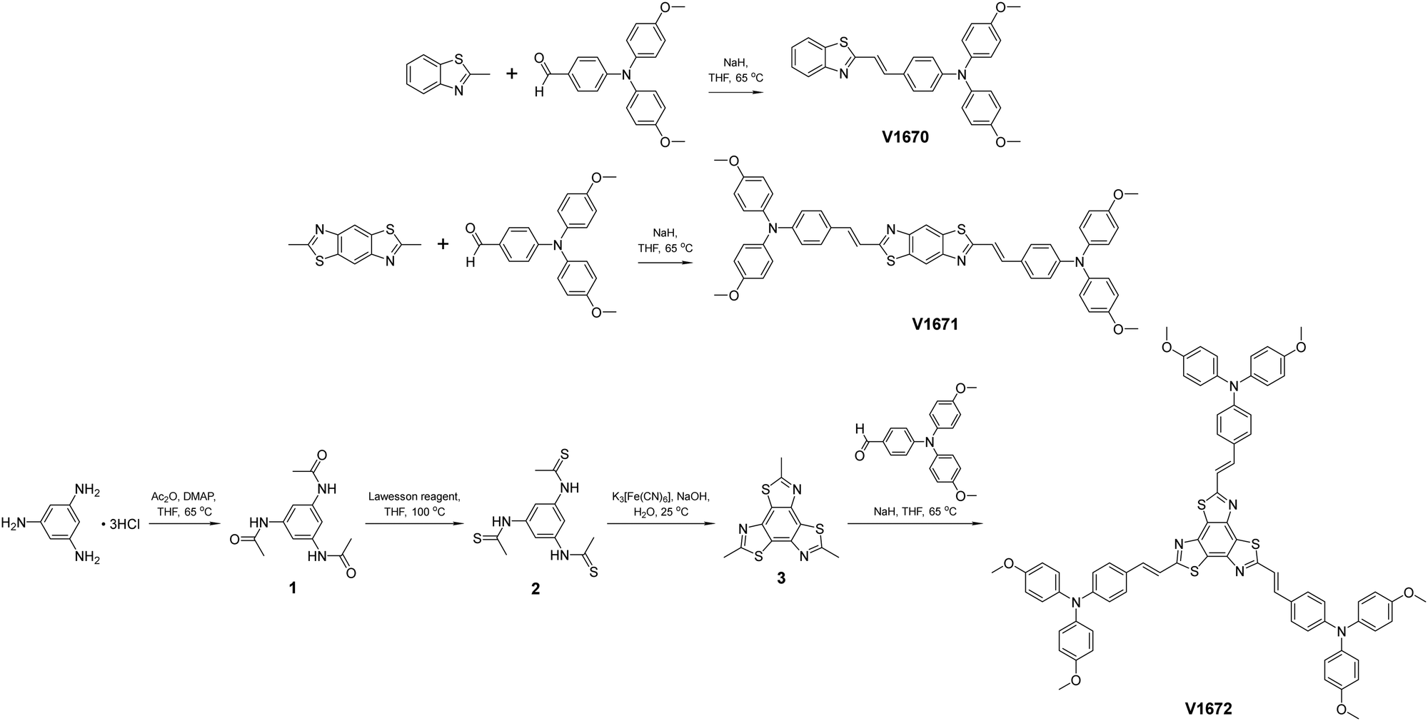 | ||
| Fig. 1 Synthesis of target compounds V1670, V1671, and V1672. | ||
The thermal stability of the prepared HTMs was examined by thermogravimetric analysis (TGA) and differential scanning calorimetry (DSC). The TGA results are provided in Fig. 2a, and the summarized properties are listed in Table 1. The TGA results show that the decomposition temperatures (Tdec) range between 362 °C and 443 °C, which is somewhat lower than that of Spiro-OMeTAD (Tdec = 449 °C).38 The increase in Tdec values has been observed in the set of the synthesized HTMs, where the lowest 5% weight loss Tdec value of 362 °C has been reported for V1670 containing one substituted triphenylamine chromophore, nevertheless, it is still reasonably high to indicate sufficient thermal stability required for PSCs. Whereas highest recorded Tdec value are for V1672 (443 °C) bearing three substituted triphenylamine chromophores. This tendency potentially can be explained by the higher molecular mass resulting in stronger intermolecular interactions.
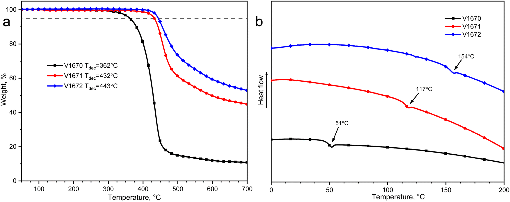 | ||
| Fig. 2 (a) TGA heating curves of the target HTMs. (b) DSC curves of the second heating run. | ||
| ID | Tga (°C) | Tdeca (°C) | λPLb (nm) | IPc (eV) | Egd (eV) | Eeae (eV) | μ0f (cm2 V−1 s−1) | μ0g (cm2 V−1 s−1) |
|---|---|---|---|---|---|---|---|---|
a Glass transition (Tg) and decomposition (Tdec) temperatures determined from DSC and TGA, respectively (10 °C min−1, N2 atmosphere).b UV-vis and PL spectra were measured in CB and CH2Cl2 (1![[thin space (1/6-em)]](https://www.rsc.org/images/entities/char_2009.gif) :1 in volume) solutions (3.3 mM).c Ionization energies of the films measured using PESA.d Eg estimated optical bandgaps of HTMs.e Eea = IP − Eg.f Mobility value at zero field strength.g Drift carrier mobility measured with bisphenol-Z polycarbonate (PC-Z) (1:1). :1 in volume) solutions (3.3 mM).c Ionization energies of the films measured using PESA.d Eg estimated optical bandgaps of HTMs.e Eea = IP − Eg.f Mobility value at zero field strength.g Drift carrier mobility measured with bisphenol-Z polycarbonate (PC-Z) (1:1). |
||||||||
| V1670 | 51 | 362 | 572 | 5.26 | 2.46 | 2.80 | 2.6 × 10⁻⁶ | 3.0 × 10⁻⁷ |
| V1671 | 117 | 432 | 593 | 5.62 | 2.23 | 3.39 | 2.7 × 10⁻⁶ | 1.4 × 10⁻⁷ |
| V1672 | 154 | 443 | 588 | 5.57 | 2.29 | 3.28 | − | 3.6 × 10⁻⁷ |
DSC analysis shows that investigated HTMs V1671 and V1672 exist in an amorphous state since no endothermic melting peaks were observed over two heating cycles (Fig. S7, ESI†). However, for the compound V1670 a melting temperature (Tm) was detected during the first heating cycle at 56 °C and glass transition temperature (Tg) was measured during the second heating at 51 °C. Meanwhile for compounds V1671 and V1672 second heating scans showed glass transition at 117 °C and 154 °C, respectively. Furthermore, the data presented in Fig. 2b and Table 1 show that the Tg values increase significantly with an increasing number of substituted triphenylamine moieties, leading to a more stabilized amorphous state, which is generally desired for the formation of stable HTM films in PSCs.38
To better understand the energy level alignment of the target compounds in PSCs, we measured the solid-state ionization potential (Ip). Ip values of the novel HTMs were determined by the photoelectron emission spectroscopy in air (PESA) measurement of their thin films and give a reliable estimation of the highest occupied molecular orbital (HOMO) energy level. The recorded data is shown in Fig. 3a and Table 1. As seen from the measurement results, Ip values of V1670, V1671 and V1672 were found to be 5.26, 5.62, and 5.57 eV, respectively. The Ip values of HTMs are sufficiently close to optimally match with the valence band energy of perovskite (∼5.7 eV), suggesting that the synthesized compounds would be suitable for use in PSCs.
 | ||
| Fig. 3 (a) Photoemission in air spectra of V1670, V1671 and V1672. (b) Electric field dependencies of the hole-drift mobility (μ) in the synthesized compounds, with and without PC-Z. | ||
The defining property of HTMs is their ability to selectively and efficiently transport holes. To investigate charge transport properties of the benzothiazole derivatives, hole drift mobilities were measured using the xerographic time of flight (XTOF) technique. The measurement results are presented in Fig. 3b and Table 1. Charge mobility values at zero-field strength (0 V cm−1) are most significant, as electric fields are relatively weak in PSCs. Although the measured charge mobility of pure compounds V1670 and V1671 was 2.6 × 10⁻⁶ and 2.7 × 10⁻⁶ cm2 V−1 s−1, respectively, which is not particularly exceptional, it is sufficient for their application in PSCs. It should be noted that the quality of pure V1672 layers was insufficient for XTOF measurements. To assess the hole drift mobility of V1672, it was mixed with a polycarbonate (PC-Z), and a film prepared. Addition of the polymer dilutes the HTM, reducing the overall charge mobility by roughly one order of magnitude; however, it allowed for the measurement of V1672 and its comparison with the other compounds. The XTOF measurement results of the HTMs with PC-Z shows that all three materials produce similar results under the same (diluted) conditions.
The PSC structure for the FTO/SnO2/Perovskite/PEAI/HTM/Au was characterized by cross-section scanning electron microscopy (SEM) (Fig. 4a). The SnO2 electron transport layers were fabricated by a chemical bath deposition (CBD) method according to a previous report.39 The energy level diagram of each component in the PSCs is illustrated in Fig. 4b. As reported above, the HOMO energy level of V1670, V1671 and V1672 are −5.26, −5.62 and −5.57 eV and the optical bandgaps are 2.46, 2.23 and 2.29 eV, respectively (Fig. S8 and S9, ESI†). Therefore, the lowest unoccupied molecular orbitals (LUMOs) of the V1670, V1671 and V1672 are calculated to be −2.80, −3.39 and −3.28 eV, respectively. The valence band maximum (VBM) and conduction band minimum (CBM) of the perovskite film are −5.71 and −4.18 eV, respectively, which were determined by ultraviolet photoelectron spectroscopy (UPS) (Fig. S10, ESI†). The HOMO level of V1671 has the lowest energy barrier relative to the VBM of the perovskite film among the three HTMs, indicating that photogenerated holes could be extracted efficiently from perovskite layer to the V1671 HTM. The PSC based on this material shows the highest PCE with the enhancement of open-circuit voltage (VOC) and short-circuit current density (JSC) among the three HTMs (Fig. S11, ESI†), which could be attributed to its efficient charge extraction property and high hole drift mobility (Table 1).
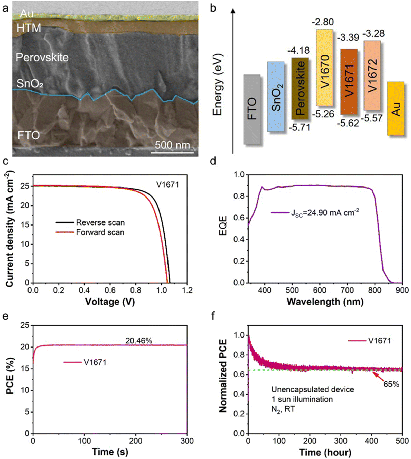 | ||
| Fig. 4 (a) The cross-sectional SEM image of the n–i–p PSC structure. (b) The energy level diagram of each layer in the PSC. (c) Current density–voltage (J–V) curves of the PSC based on the V1671 HTM under reverse and forward scan modes. (d) External quantum efficiency (EQE) spectra and the integrated JSC of the corresponding PSC. (e) Steady power output of the champion target device for 300 s. (f) MPP tracking of the unencapsulated V1671 PSC under continuous 1 Sun illumination in a N2 atmosphere at room temperature. | ||
The surface morphologies of the V1670, V1671 and V1672 films were measured by SEM, as shown in Fig. S12 (ESI†). The surface morphology of the V1670 is highly homogeneous, whereas the V1671 film is slightly less homogeneous and not pinhole-free. However, the V1672 film has poor morphology, with many visible pinholes and a tendency to aggregate when spin-coating, which may affect the quality of HTM film and impede the PSC performance. Fig. S15 (ESI†) shows the TRPL spectra of perovskite and deposited HTLs. The effective lifetimes (defined as the time required for the PL intensity to decay to 1/e of its initial value after excitation) were 86.8, 1.8, 2.2, and 2.9 ns for the perovskite, perovskite/V1670, perovskite/V1671, and perovskite/V1672 films, respectively. Compared to the pristine perovskite film, the perovskite/HTM films exhibit much shorter PL lifetimes, indicating efficient carrier extraction at the perovskite/HTM interface. Among the three HTMs, V1671 shows the most efficient carrier extraction, consistent with its minimal energy barrier between its HOMO level and the VBM of the perovskite.
Further, the performance of the PSC based on V1671 was optimized by adjusting its solution concentration during spin-coating (Fig. S13, ESI†) and the average photovoltaic parameters are summarized in Table S1 (ESI†). The PSCs based on 25 mg mL−1 V1671 have the best surface morphology, and, correspondingly, the highest photovoltaic performance (Fig. S12b and S14, ESI†). A V1671 concentration above 30 mg mL−1 led to significant reductions in JSC and fill factor (FF) of the PSCs due to reduced homogeneity of the surface. The champion V1671 device had a VOC of 1.066 V, a JSC of 25.10 mA cm−2 and an FF of 77.6%, which resulted in a PCE of 20.74% at reverse scan (RS) (Fig. 4c). Its PCE at forward scan (FS) reached 19.62%. Detailed photovoltaic parameters are summarized in Table 2. The hysteresis index (HI) of the V1671 device was 5.4%, as calculated using HI = (PCERS − PCEFS)/PCERS.34 Compared to the V1671 device, the Spiro-OMeTAD device shows a higher PCE of 21.8% with a smaller HI of 3.2% (Fig. S16, ESI†), indicating there is still a gap of molecular design. Fig. 4d shows the spectral dependence of the external quantum efficiency (EQE) for the V1671 device. The integrated current density is 24.90 mA cm−2, which is consistent with the JSC value in Fig. 4c. Furthermore, the maximum power point tracking (MPPT) PCE of the device is 20.46%, stable over a 300 s measurement (Fig. 4e). In addition, the operational stability of the unencapsulated V1671 device was evaluated at the MPP under a nitrogen atmosphere using a light-emitting diode lamp with a calibrated light intensity of 100 mW cm−2. After 500 hours of measurement, the V1671 device retained about 65% of its initial PCE (Fig. 4f). Water contact angle measurements revealed that all HTMs show higher contact angle comparing with bare perovskite films as shown in Fig. S17 (ESI†). V1671 film exhibited a highest angle (83°) among the series, which is also higher than that of the spiro-OMeTAD (68°).40 The greater hydrophobicity of V1671 could be one of the reasons of high stability of the device that contains this HTM.
| V1671 | VOC (V) | JSC (mA cm−2) | FF (%) | PCE (%) |
|---|---|---|---|---|
| Reverse | 1.066 | 25.10 | 77.6 | 20.74 |
| Forward | 1.046 | 25.21 | 74.5 | 19.62 |
Conclusions
In conclusion, we report the synthesis and systematic study of the novel A(–π–D)n type small molecule HTMs for PSCs. The investigated benzothiazole-based arylamines were obtained in high yield via a simple Knoevenagel condensation reaction. The influence of the different number of triphenylamine chromophores has been evaluated by the thermal, optical, photophysical and photovoltaic measurements. It was found that as the number of triphenylamine fragments increases the decomposition and glass transition temperatures of the HTMs increase, and investigated compounds exist in an amorphous state which is desired in the fabrication of PSCs. Notably, the Ip values of HTMs are in the range of 5.26–5.62 eV, which is suitable for application in PSCs. Additionally, PSCs fabricated with V1671 as the HTM resulted in the photovoltaic device achieving a PCE of 20.74% that is much higher than PCEs of V1670 and V1672 devices, which could be attributed to its higher hole drift mobility, better energy level alignment relative to the perovskite layer, and pinhole-free surface morphology. This work shows that the synthesis of new small molecule HTMs via a donor–π-bridge–acceptor type-strategy is an effective method to improve the performance of the hole transporting layer in PSCs.Data availability
The data that supports the findings of this study are available within the article and its ESI.† Additional data will be available online under repository link once the article will be accepted for publication, or from the corresponding author upon request. We note that there are not any restrictions on data availability (e.g., proprietary data, privacy concerns).Conflicts of interest
There are no conflicts to declare.Acknowledgements
We acknowledge the project “Technological and Physical Sciences Excellence Centre (TiFEC)” No. S-A-UEI-23-1, which was funded by the Science Council of Lithuania and the Ministry of Education, Science and Sports of the Republic of Lithuania from the state budget under the programme “University Excellence Initiative.” We also acknowledge the EPFL financial support.References
- G. Hodes, Science, 1979, 2013(342), 317–318 Search PubMed.
- A. Kojima, K. Teshima, Y. Shirai and T. Miyasaka, J. Am. Chem. Soc., 2009, 131, 6050–6051 CrossRef CAS PubMed.
- NREL, Best Research-Cell Efficiency Chart, https://www.nrel.gov/pv/assets/pdfs/best-research-cell-efficiencies.pdf, (accessed 3 February 2025).
- Y. Rong, Y. Hu, A. Mei, H. Tan, M. I. Saidaminov, S. Il Seok, M. D. McGehee, E. H. Sargent and H. Han, Science, 2018, 361, eaat8235 CrossRef PubMed.
- W. Nie, H. Tsai, R. Asadpour, J.-C. Blancon, A. J. Neukirch, G. Gupta, J. J. Crochet, M. Chhowalla, S. Tretiak, M. A. Alam, H.-L. Wang and A. D. Mohite, Science, 2015, 347, 522–525 CrossRef CAS PubMed.
- S. Park, J. H. Heo, C. H. Cheon, H. Kim, S. H. Im and H. J. Son, J. Mater. Chem. A, 2015, 3, 24215–24220 RSC.
- S. Kazim, M. K. Nazeeruddin, M. Grätzel and S. Ahmad, Angew. Chem., Int. Ed., 2014, 53, 2812–2824 CrossRef CAS PubMed.
- N.-G. Park, J. Phys. Chem. Lett., 2013, 4, 2423–2429 CrossRef CAS.
- R. Sharma, A. Sharma, S. Agarwal and M. S. Dhaka, Sol. Energy, 2022, 244, 516–535 CrossRef CAS.
- A. S. R. Bati, Y. L. Zhong, P. L. Burn, M. K. Nazeeruddin, P. E. Shaw and M. Batmunkh, Commun. Mater., 2023, 4, 2 CrossRef CAS.
- M. Afroz, R. K. Ratnesh, S. Srivastava and J. Singh, Sol. Energy, 2025, 287, 113205 CrossRef CAS.
- A. Jegorovė, M. A. Truong, R. Murdey, M. Daskeviciene, T. Malinauskas, K. Kantminiene, V. Jankauskas, V. Getautis and A. Wakamiya, Solar RRL, 2022, 6, 2100877 CrossRef.
- E. Kasparavicius, M. Franckevičius, V. Malinauskiene, K. Genevičius, V. Getautis and T. Malinauskas, ACS Appl. Energy Mater., 2021, 4, 13696–13705 CrossRef CAS PubMed.
- T. Malinauskas, M. Saliba, T. Matsui, M. Daskeviciene, S. Urnikaite, P. Gratia, R. Send, H. Wonneberger, I. Bruder, M. Graetzel, V. Getautis and M. K. Nazeeruddin, Energy Environ. Sci., 2016, 9, 1681–1686 RSC.
- R. Tiazkis, S. Paek, M. Daskeviciene, T. Malinauskas, M. Saliba, J. Nekrasovas, V. Jankauskas, S. Ahmad, V. Getautis and M. Khaja Nazeeruddin, Sci. Rep., 2017, 7, 150 CrossRef PubMed.
- M. L. Petrus, K. Schutt, M. T. Sirtl, E. M. Hutter, A. C. Closs, J. M. Ball, J. C. Bijleveld, A. Petrozza, T. Bein, T. J. Dingemans, T. J. Savenije, H. Snaith and P. Docampo, Adv. Energy Mater., 2018, 8, 1801605 CrossRef.
- D. Vaitukaityte, Z. Wang, T. Malinauskas, A. Magomedov, G. Bubniene, V. Jankauskas, V. Getautis and H. J. Snaith, Adv. Mater., 2018, 30, 1803735 CrossRef PubMed.
- M. Daskeviciene, S. Paek, Z. Wang, T. Malinauskas, G. Jokubauskaite, K. Rakstys, K. T. Cho, A. Magomedov, V. Jankauskas, S. Ahmad, H. J. Snaith, V. Getautis and M. K. Nazeeruddin, Nano Energy, 2017, 32, 551–557 CrossRef CAS.
- M. Daskeviciene, S. Paek, A. Magomedov, K. T. Cho, M. Saliba, A. Kizeleviciute, T. Malinauskas, A. Gruodis, V. Jankauskas, E. Kamarauskas, M. K. Nazeeruddin and V. Getautis, J. Mater. Chem. C, 2019, 7, 2717–2724 RSC.
- C. Lu, I. T. Choi, J. Kim and H. K. Kim, J. Mater. Chem. A, 2017, 5, 20263–20276 RSC.
- A. Magomedov, S. Paek, P. Gratia, E. Kasparavicius, M. Daskeviciene, E. Kamarauskas, A. Gruodis, V. Jankauskas, K. Kantminiene, K. T. Cho, K. Rakstys, T. Malinauskas, V. Getautis and M. K. Nazeeruddin, Adv. Funct. Mater., 2018, 28, 1704351 CrossRef.
- K. Radhakrishna, S. B. Manjunath, D. Devadiga, R. Chetri and A. T. Nagaraja, ACS Appl. Energy Mater., 2023, 6, 3635–3664 CrossRef CAS.
- J. Xia, P. Luizys, M. Daskeviciene, C. Xiao, K. Kantminiene, V. Jankauskas, K. Rakstys, G. Kreiza, X. Gao, H. Kanda, K. G. Brooks, I. R. Alwani, Q. U. Ain, J. Zou, G. Shao, R. Hu, Z. Qiu, A. Slonopas, A. M. Asiri, Y. Zhang, P. J. Dyson, V. Getautis and M. K. Nazeeruddin, Adv. Mater., 2023, 35, 2300720 CrossRef CAS PubMed.
- A. Farokhi, H. Shahroosvand, G. D. Monache, M. Pilkington and M. K. Nazeeruddin, Chem. Soc. Rev., 2022, 51, 5974–6064 RSC.
- D. Li, J.-Y. Shao, Y. Li, Y. Li, L.-Y. Deng, Y.-W. Zhong and Q. Meng, Chem. Commun., 2018, 54, 1651–1654 RSC.
- X. Zhang, X. Liu, F. F. Tirani, B. Ding, J. Chen, G. Rahim, M. Han, K. Zhang, Y. Zhou, H. Quan, B. Li, W. Du, K. G. Brooks, S. Dai, Z. Fei, A. M. Asiri, P. J. Dyson, M. K. Nazeeruddin and Y. Ding, Angew. Chem., Int. Ed., 2024, 63, e202320152 CrossRef CAS PubMed.
- M. SasiKumar, G. Maddala, M. Ambapuram, M. Subburu, J. R. Vaidya, S. N. Babu, P. Chetti, R. Mitty and S. Pola, Sustainable Energy Fuels, 2020, 4, 4754–4767 RSC.
- K. Manda, V. D. Jadhav, P. Chetti, R. Gundla and S. Pola, Org. Electron., 2025, 136, 107153 CrossRef CAS.
- G. Maddala, R. Gade, J. Ahemed, S. Kalvapalli, N. B. Simhachalam, P. Chetti, S. Pola and R. Mitty, Sol. Energy, 2021, 226, 501–512 CrossRef CAS.
- D. Bharath, M. Sasikumar, N. R. Chereddy, J. R. Vaidya and S. Pola, Sol. Energy, 2018, 174, 130–138 CrossRef CAS.
- A. Zhang, Y. Chen, Y. Xu, H. Wang, X. Zong, Z. Sun, M. Liang and S. Xue, ACS Appl. Energy Mater., 2024, 7, 11741–11753 CrossRef CAS.
- G. Zhang, F. R. Lin, F. Qi, T. Heumüller, A. Distler, H.-J. Egelhaaf, N. Li, P. C. Y. Chow, C. J. Brabec, A. K.-Y. Jen and H.-L. Yip, Chem. Rev., 2022, 122, 14180–14274 CrossRef CAS PubMed.
- Y. Liu, Q. Chen, H.-S. Duan, H. Zhou, Y. Michael Yang, H. Chen, S. Luo, T.-B. Song, L. Dou, Z. Hong and Y. Yang, J. Mater. Chem. A, 2015, 3, 11940–11947 RSC.
- C. Steck, M. Franckevičius, S. M. Zakeeruddin, A. Mishra, P. Bäuerle and M. Grätzel, J. Mater. Chem. A, 2015, 3, 17738–17746 RSC.
- E. Sheibani, L. Yang and J. Zhang, Solar RRL, 2020, 4, 2000461 CrossRef CAS.
- H. D. Pham, S. M. Jain, M. Li, Z. Wang, S. Manzhos, K. Feron, S. Pitchaimuthu, Z. Liu, N. Motta, J. R. Durrant and P. Sonar, Adv. Electron. Mater., 2020, 6, 1900884 CrossRef CAS.
- A. Fülöpová, P. Magdolen, M. Károlyiová, I. Sigmundová and P. Zahradník, J. Heterocycl. Chem., 2013, 50, 563–567 CrossRef.
- T. Malinauskas, D. Tomkute-Luksiene, R. Sens, M. Daskeviciene, R. Send, H. Wonneberger, V. Jankauskas, I. Bruder and V. Getautis, ACS Appl. Mater. Interfaces, 2015, 7, 11107–11116 CrossRef CAS PubMed.
- S. Tian, X. Gao, D. Reyes, O. A. Syzgantseva, M. M. Baytemirov, N. Shibayama, H. Kanda, P. A. Schouwink, Z. Fei, L. Zhong, F. F. Tiranito, Y. Fang, P. J. Dyson and M. K. Nazeeruddin, Small, 2024, 20, 2406929 CrossRef CAS PubMed.
- A. Jegorovė, J. Xia, M. Steponaitis, M. Daskeviciene, V. Jankauskas, A. Gruodis, E. Kamarauskas, T. Malinauskas, K. Rakstys, K. A. Alamry, V. Getautis and M. K. Nazeeruddin, Chem. Mater., 2023, 35, 5914–5923 CrossRef PubMed.
Footnotes |
| † Electronic supplementary information (ESI) available. See DOI: https://doi.org/10.1039/d5tc01318f |
| ‡ P. L. and S. T. contributed equally to this work. |
| This journal is © The Royal Society of Chemistry 2025 |