
 Open Access Article
 This Open Access Article is licensed under a
 Creative Commons Attribution 3.0 Unported Licence
Engineered semiconductor-dielectric interfaces in polymer ferroelectric transistors†
Arash Ghobadi a,
Thomas B. Kallaosa,
Indeewari M. Karunarathnea,
Dilan M. Gamachchia,
Andrew C. Mengab,
Joseph C. Mathaic,
Shubhra Gangopadhyayc and
Suchismita Guha*ab
a,
Thomas B. Kallaosa,
Indeewari M. Karunarathnea,
Dilan M. Gamachchia,
Andrew C. Mengab,
Joseph C. Mathaic,
Shubhra Gangopadhyayc and
Suchismita Guha*ab
aDepartment of Physics and Astronomy, University of Missouri, Columbia, MO 65211, USA. E-mail: guhas@missouri.edu
bMU Materials Science and Engineering Institute, University of Missouri, Columbia, MO 65211, USA
cDepartment of Electrical Engineering and Computer Science, University of Missouri, Columbia, MO 65211, USA
First published on 30th May 2025
Abstract
Polymer ferroelectrics are witnessing a renewed interest in organic transistors due to their multi-conductance states. Although their high dielectric constant allows low operating voltages, the polarization fluctuation due to the energetic disorder at the interface reduces the carrier mobility in organic transistors. Here, two copolymers of poly(vinylidene fluoride) (PVDF) with trifluoroethylene (TrFE) and hexafluoropropylene (HFP) as the dielectric layer, and a donor–acceptor copolymer as the active semiconductor layer are used in bottom-gate top-contact transistor architectures. We investigate the impact of the dielectric thickness, external poling, and an added interfacial ultrathin Al2O3 layer at the semiconductor-dielectric surface on the performance of organic field-effect transistors (FETs). Although poling the dielectric layer significantly enhances the carrier mobility in PVDF-TrFE-based FETs, it has a minimal effect on PVDF-HFP-based devices. Poled PVDF-TrFE devices with a thickness of 45 nm show the highest saturation carrier mobility, exceeding 1 cm2 V−1 s−1. The subthreshold swing (SS), which is primarily governed by the trap states at the semiconductor–dielectric interface, is seen to significantly improve when an atomic layer deposited Al2O3 film with varying thickness between 2 nm and 12 nm is deposited on PVDF-HFP. In the linear region of operation, PVDF-HFP based FETs with Al2O3 yield SS values below 80 mV dec−1. The trap density of states at the semiconductor–dielectric interface was evaluated, providing deeper insight into charge trapping and transport mechanisms.
Introduction
The high dielectric constant (κ) of oxide and ferroelectric dielectrics provides a path towards low-operating voltage organic field-effect transistors (FETs),1 especially since they work in the accumulation region. At the semiconductor–dielectric interface, the dielectric layer not only influences the morphology of the semiconducting layer, but it also changes the density of states (DOS) due to local polarization effects.2–4 Polarizable gate dielectrics, for example, broaden the DOS at the semiconductor–dielectric interface due to charge–dipole coupling and increase the localization of carriers at the interface.5,6 These effects reduce the carrier mobility in FETs at the cost of achieving low operating voltages with high κ dielectrics. Another route for low operating voltage organic FETs is to reduce the thickness of the dielectric layer. Several strategies involving stacked self-assembled monolayers and AlOx as ultrathin layers, with thicknesses typically less than 20 nm, have demonstrated operating voltages less than 5 V in organic FETs.7–9 However, most of these examples use small molecule organic semiconductors. Moreover, such stacked dielectrics require oxidation or anodization processes to form the AlOx layer. In addition to low voltage, practical applications of organic FETs demand low subthreshold swing (SS) and high carrier mobilities. Although the carrier mobility in polymeric semiconductors is limited due to the hopping nature of transport between disordered-localized states,10,11 other factors such as a polarizable dielectric layer12,13 and the source/drain contacts14,15 strongly influence charge transport properties in FET architectures. Hence, the same semiconductor may display a wide range of carrier mobilities as κ is tuned from low to high. Several strategies for contact modification including adding self-assembled monolayers have resulted in a remarkable reduction of contact resistance in the tens of Ω cm.16–18 Approaches for reducing the Schottky barrier by de-pinning the Fermi level in organic FETs have involved introduction of oxygen at the metal-semiconductor surface in p-type transport19 and adding ultrathin Al2O3 on the metal contacts for both p- and n-type transport in organic FETs.20Ideally, ferroelectric dielectrics could be of great benefit for low operating voltage organic FETs, especially if the polarization fluctuation can be reduced, they are thin, they are solvent compatible with π-conjugated small molecules and polymers, and the trap-DOS at the semiconductor–ferroelectric interface can be lowered. These conditions would permit enhanced switching efficiencies by lowering SS. Further, the choice of a solution processable dielectric and a semiconducting layer allows low-cost fabrication methods. This work focusses on solution processable ferroelectrics and a donor–acceptor copolymer, diketopyrrolopyrrole (dithienylthieno[3,2-b]thiophene (DPP-DTT)), for improving the semiconductor–dielectric interface in organic FETs. Since the devices are bottom-gate with top-contact, no additional contact treatment was performed.
Among polymer ferroelectrics, the copolymers of polyvinylidene fluoride (PVDF) have been extremely popular as dielectric layers in organic FETs for applications in memory devices,21–24 sensors,25–27 and more recently in neuromorphic devices.28,29 Copolymers of PVDF with trifluoroethylene (PVDF-TrFE) and hexafluoropropylene (PVDF-HFP) have differences in their ferroelectric properties, although their κ values are similar at room temperature. The ferroelectricity in PVDF and its copolymers originate from the β phase, where the carbon atoms are in an all-trans-configuration, and the paraelectric α phase arises from a trans–gauche conformation.30 PVDF-TrFE upon spincasting from a solution is already in the β phase and, therefore, metal–insulator–metal capacitors made with PVDF-TrFE show typical hysteresis loops in the polarization versus voltage curves, expected from a ferroelectric film.31,32 PVDF-HFP, on the other hand, is an elastomer with a higher component of the α phase compared with the β phase.33,34 Typical saturation polarization values are 6 μC cm−2 and 3 μC cm−2 for PVDF-TrFE and PVDF-HFP, respectively (see ESI†).35 With similar values of κ but differences in their ferroelectric properties, PVDF-TrFE and PVDF-HFP allow an excellent comparison for monitoring the semiconductor–dielectric interfaces in organic FETs.
Our prior work demonstrated that by externally poling the PVDF-TrFE film in the vertical direction, prior to the fabrication of organic FETs, and using DPP-DTT as the active semiconductor layer, improves both carrier mobility and SS if the poling field is <100 mV m−1. Differential phase contrast (DPC) images in the scanning transmission electron microscope (STEM) indicated that the vertically poled PVDF-TrFE films have uniform ferroelectric domains throughout the bulk of the film.36 Polarization domains are also seen in the DPC images from the unpoled film, except they are significantly more disordered. The higher mobility in the poled devices could be rationalized by a lower trap DOS, as determined by the Grünewald's method,37,38 compared with the unpoled devices. The operating voltage in this study was 20 V. Further reduction of the operating voltage demands lowering the thickness of the polymer ferroelectric layer.
In this work we use two approaches for improving the ferroelectric-DPP-DTT interface. The first is to reduce the dielectric thickness to below 50 nm. The second approach is to add a thin (2–12 nm) atomic layer deposited Al2O3 layer on top of the ferroelectric layer. The operating voltages are below 8 V for both PVDF-TrFE and PVDF-HFP based FETs, which operate as p-type devices. Vertically poling the PVDF-TrFE layer (with thickness ∼45 nm) improves carrier mobilities to >1 cm2 V−1 s−1. However, there is a marginal difference in the carrier mobilities between the vertically poled and unpoled PVDF-HFP films. In an effort to further lower the SS, we deposited a thin layer of Al2O3 by atomic layer deposition on top of the ferroelectric layer. No significant improvement in SS was observed with PVDF-TrFE when 2 nm, 3 nm, and 5 nm of Al2O3 were deposited. Additionally, the carrier mobilities are also seen to be lower than that of the unpoled devices. There is a significant improvement in SS for the PVDF-HFP devices with the layer of Al2O3, highlighting the role of the oxide layer in passivating defect sites. Trap DOS calculations show lower trap densities for PVDF-TrFE compared with PVDF-HFP FETs. A similar distribution of shallow traps in as-is PVDF-HFP and with the thin Al2O3 layer are observed, highlighting the influence of the oxide layer on the deep-level traps. Cross-sectional STEM images show the same morphology in the bulk of the semiconductor with and without the Al2O3 layer.
Experimental methods and analysis
Materials
Poly(vinylidene fluoride-trifluoroethylene) (PVDF-TrFE) (75![[thin space (1/6-em)]](https://www.rsc.org/images/entities/char_2009.gif) :25) and poly(vinylidene fluoride-co-hexafluoropropylene) (PVDF-HFP) (Mw = 455000) were purchased from PolyK Technologies Inc. and Sigma-Aldrich, respectively. The donor–acceptor copolymer DPP-DTT was obtained from 1-Material Inc. (Dorval, Quebec, Canada). N,N-Dimethylformamide (DMF) and 1,2-dichlorobenzene (DCB) (anhydrous, 98%) were sourced from Sigma-Aldrich (St. Louis, MO, USA).
:25) and poly(vinylidene fluoride-co-hexafluoropropylene) (PVDF-HFP) (Mw = 455000) were purchased from PolyK Technologies Inc. and Sigma-Aldrich, respectively. The donor–acceptor copolymer DPP-DTT was obtained from 1-Material Inc. (Dorval, Quebec, Canada). N,N-Dimethylformamide (DMF) and 1,2-dichlorobenzene (DCB) (anhydrous, 98%) were sourced from Sigma-Aldrich (St. Louis, MO, USA).
Device fabrication
The device structure is bottom-gate, top-contact with a patterned Al layer as the gate electrode, the PVDF copolymers as the dielectric layer, followed by DPP-DTT as the semiconductor. Top Au contacts served as the source and drain. A 50 nm Al gate electrode was thermally evaporated onto 1′′ × 1′′ glass substrates using a patterned mask following an organic cleaning process. The dielectric solutions were prepared by dissolving PVDF-TrFE and PVDF-HFP in DMF at a concentration of 100 mg mL−1, heated to 80 °C for 3 hours, and subsequently stirred at room temperature overnight. The solutions were diluted to 50 mg mL−1 for the thinner dielectric films. Under a nitrogen atmosphere, the diluted solutions were statically dispensed onto the pre-deposited Al gate and spin-coated at 1600 rpm for 60 seconds to ensure uniformity. The coated substrates were then annealed at 70 °C for 10 minutes in a nitrogen environment to facilitate solvent evaporation, resulting in a dielectric film thickness of approximately 45 nm.Each substrate was placed on a hotplate under ambient conditions for the poling process. A thin Al strip was positioned on top of the PVDF-TrFE or PVDF-HFP film for the application of an electric field (40 MV m−1 for the thinner films) between the underlying Al gate and the external Al contact. The poling was conducted at 135 °C, close to the Curie temperature of PVDF-TrFE and PVDF-HFP, to enhance dipole reorientation. The applied field was maintained as the substrates cooled to room temperature to preserve the dipole alignment.
DPP-DTT solution was prepared by dissolving DPP-DTT in DCB at a concentration of 5 mg mL−1. The solution was subjected to sequential heating at 100 °C for 1 hour, 130 °C for 1 hour, and 145 °C for over 12 hours while stirring at 200 RPM. After overnight stirring at room temperature, the solution was filtered through a 0.45 μm PTFE filter and reheated for 30 minutes before spincasting. Under a nitrogen atmosphere, 75 μL of the DPP-DTT solution was dynamically spin-coated onto the ferroelectric layer at 900 rpm for 60 seconds. A Teflon tape was employed to confine the semiconducting film to a defined channel region during spin-coating and was removed before annealing the film at 120 °C for 1 hour under nitrogen. Finally, a 50 nm Au layer was thermally evaporated through a patterned mask to define the source and drain electrodes. Each substrate contained four devices with a fixed channel width of 1000 μm and channel lengths of 50 μm, 75 μm, 100 μm, and 125 μm.
Al2O3 deposition
Al2O3 layers of varying thicknesses were deposited on top of PVDF-TrFE and PVDF-HFP using a Cambridge NanoTech S200 atomic layer deposition (ALD) system. The process employed trimethylaluminum (TMA) and deionized water (DI-water), both obtained from Sigma-Aldrich. The chamber was maintained at 150 °C, which was the optimum temperature that preserves the integrity of the underlying dielectric layer while ensuring sufficient Al2O3 growth. Following sample loading, a continuous nitrogen (N2) flow of 5 sccm was introduced into the chamber and subsequently increased to 20 sccm. The deposition was performed over 22, 33, 55, 88, and 132 ALD cycles to achieve film thicknesses of 2, 3, 5, 8, and 12 nm, respectively. Each cycle consisted of a 0.01 s pulse of DI-water, a 20 s N2 purge, a 0.015 s pulse of TMA vapor, followed by another 20 s N2 purge. Upon completion, the N2 flow rate was reduced to 5 sccm.Characterization
Current–voltage measurements were performed at room temperature using a Keithley 4200A-SCS parameter analyzer. Scanning/transmission electron microscope (STEM) imaging was performed using a probe aberration corrected ThermoFisher Spectra 300 scanning/transmission electron microscope. TEM cross-section lift out and thinning were performed in a ThermoFisher Helios Hydra UX DualBeam plasma focused ion beam (PFIB) using Xe+ as the ion source at 30 kV accelerating voltage. Sample thinning was performed using Ar+ as the ion source at 30 kV, with final thinning performed at 8 kV. The capacitance and conductance measurements were carried out using an HP 4284 LCR meter. The AFM images were acquired by Brucker (model: Innova).Transistor parameters and trap density of states analysis
The carrier mobility was extracted from the current–voltage transfer characteristics in the saturation and linear region using the standard MOSFET equations. The drain current (ID) in the saturation region is given by: ID(sat) = (W/2L)μCi(VGS − Vth)2, where W and L are the channel width and length, respectively. Ci is the capacitance/area of the dielectric, VGS is the gate-source voltage and Vth is the threshold voltage. Hence, the saturation mobility is . In the linear region, ID(lin) = (W/L)μCi[(VGS − Vth)2 − VDS2/2], and thus, the carrier mobility in this region is μlin = (L/CiWVDS)(∂ID/∂VGS). The subthreshold swing (SS) is given by SS = dVGS/(logIDS), which gives an upper limit for the interface trap states (Nint) such that SS = kTlog10/e[1 + (e2/Ci)Nint], where k is the Boltzmann constant and T is the temperature. For state-of-the-art MOSFETs, SS is typically 70 mV decade−1 (dec).
The contact resistance was determined using the transmission line method (TLM). The contact resistance (RC) normalized with W is related to the total resistance (R) in the channel and is given by RW = RCW + L/μeffCi(VGS − Vth), where μeff is the channel mobility free from the contact resistance.
The trap DOS was analyzed using the Grünewald's method.37,38 The gate-dependent dielectric–semiconductor interface potential V0 = V0(Ug) is first determined from:
 | (1) |
 | (2) |
 | (3) |
Results and discussions
Dielectric thickness and poling
The semiconductor was DPP-DTT and all FETs were fabricated using a bottom-gate, top-contact geometry. Fig. 1(a) shows a schematic of the FET where both PVDF-TrFE and PVDF-HFP were used as the dielectric layer. Vertical poling was achieved by applying an electric field of either 100 MV m−1 for the thicker dielectric layer (∼125 nm) and 40 MV m−1 for the thinner dielectric layer (∼45 nm) at the Curie temperature, as shown in Fig. 1(b). The field is applied in a direction such that the dipole moments of the ferroelectric domains point vertically downwards. This facilitates the accumulation of hole carriers at the semiconductor–dielectric interface, which is advantageous for p-type transport in DPP-DTT. Fig. 1(c)–(e) compares the transfer and output characteristics of a vertically poled and unpoled PVDF-TrFE FET. The dotted line in the transfer curve is a linear fit where the intercept yields Vth. The dielectric thickness was ∼125 nm. The vertically poled PVDF-TrFE FET demonstrates three times higher saturation carrier mobility compared with the unpoled device. Earlier work highlighted that vertically poled PVDF-TrFE based organic FETs show a significant improvement in carrier mobilities and other transistor properties.39 An additional lateral poling of the bottom half of the PVDF-TrFE layer to an already vertically poled film minimizes the gate leakage current in TIPS-pentacene FETs, further enhancing the carrier mobility.40 DPC images have revealed uniform polarization domains in vertically poled PVDF-TrFE films with almost no localization of the polarization domains at the interface.36 This reduces the overall polarization fluctuation in transport, enhancing carrier mobility in vertically poled FETs. | ||
| Fig. 1 (a) Device schematic where the dielectric thickness was reduced from 125 nm to below 50 nm. Chemical structure of PVDF-TrFE and PVDF-HFP. (b) Vertical poling of the dielectric layer was carried out by applying an electric field at a temperature of ∼135 °C. (c) and (d) Transfer and output characteristics of an unpoled PVDF-TrFE/DPP-DTT FET, respectively. (e) and (f) Transfer and output characteristics of a vertically poled PVDF-TrFE/DPP-DTT FET, respectively. The dielectric thickness was ∼125 nm for both poled and unpoled devices. | ||
Next, the thickness of the dielectric layer was reduced to ∼45 nm for lowering the operating voltage of the FETs. Fig. 2 shows the transfer characteristics from four such devices with PVDF-TrFE and PVDF-HFP, both unpoled and poled. In all cases, the saturation characteristics are observed by −7 V. The output characteristics of these four devices are shown in ESI† (Fig. S1). The poled PVDF-TrFE FET shows a saturation carrier mobility (μsat) of 1.24 cm2 V−1 s−1 compared with 0.3 cm2 V−1 s−1 for the unpoled device. The histogram of μsat from several poled PVDF-TrFE devices shows a mean value >1 cm2 V−1 s−1 (Fig. S2, ESI†). The SS value is also lowered for the poled PVDF-TrFE FET. In contrast, poling does not seem to enhance the PVDF-HFP FET performance. There is almost no difference in μsat (∼0.28 cm2 V−1 s−1) between poled and unpoled PVDF-HFP. Since the overall ferroelectricity in PVDF-HFP is lower than in PVDF-TrFE, external electrical field poling seems to have almost no impact in orienting the polarization domains.
 | ||
| Fig. 2 Transfer characteristics of DPP-DTT FETs with a dielectric thickness of 45 nm. (a) Unpoled PVDF-TrFE, (b) poled PVDF-TrFE, (c) unpoled PVDF-HFP, and (d) poled PVDF-HFP. | ||
Although the value of SS is an indicator of the trap density, it mainly probes the deeper bandgap states as the quasi-Fermi level is far from the band-edge in the subthreshold region. The trap DOS estimated from the Grünewald's method allows an estimation of the shallow trap states. Polymeric semiconductors are usually described by a Gaussian distribution of traps as sketched in Fig. 3(a). Since disorder in these systems results in electron localization, it has a Gaussian distribution. The mobility edge in a polymeric semiconductor acts as the band edge in a crystalline material. In addition to the shallow trap states, localized deep states are present. If the Fermi level is located in the region of the localized states (near the green peaks in Fig. 3(a)), conductivity at high temperatures can arise from thermal excitation of carriers across the mobility gap in addition to hopping of carriers due to the shallow trap states. We estimate the trap DOS using the Grünewald's method from the valence band edge (EV), which is the HOMO level, for PVDF-TrFE and PVDF-HFP FETs, as illustrated in Fig. 3(b) and (c). The trap DOS is almost an order of magnitude higher near the band edge for the thicker unpoled (125 nm) PVDF-TrFE FET compared with the thinner (45 nm) unpoled one. Additionally, the trap DOS for the vertically poled PVDF-TrFE FET is lower compared with the unpoled one. On the other hand, unpoled and poled PVDF-HFP (of thickness 45 nm) FETs show similar trap DOS. It should be noted that vertically poled PVDF-TrFE displays a very different morphology with distinct domains compared with its unpoled counterpart.39 Hence, it is not surprising that their trap DOS differ. We further estimate the interface trap density (Dit) from capacitance and conductance versus voltage measurements from PVDF-TrFE based metal–insulator–semiconductor (MIS) diodes for a comparison of the unpoled and poled layers. The Dit values are determined from the loss as the occupancy of the interface trap states change with the gate bias.41 Using a continuum of state model,42 the Dit values obtained at the flat-band voltage are 2.3 × 10¹² eV−1 cm−2 and 3.5 × 10¹² eV−1 cm−2 for the poled and unpoled PVDF-TrFE MIS diodes, respectively. See ESI† for details (Fig. S8 and S9).
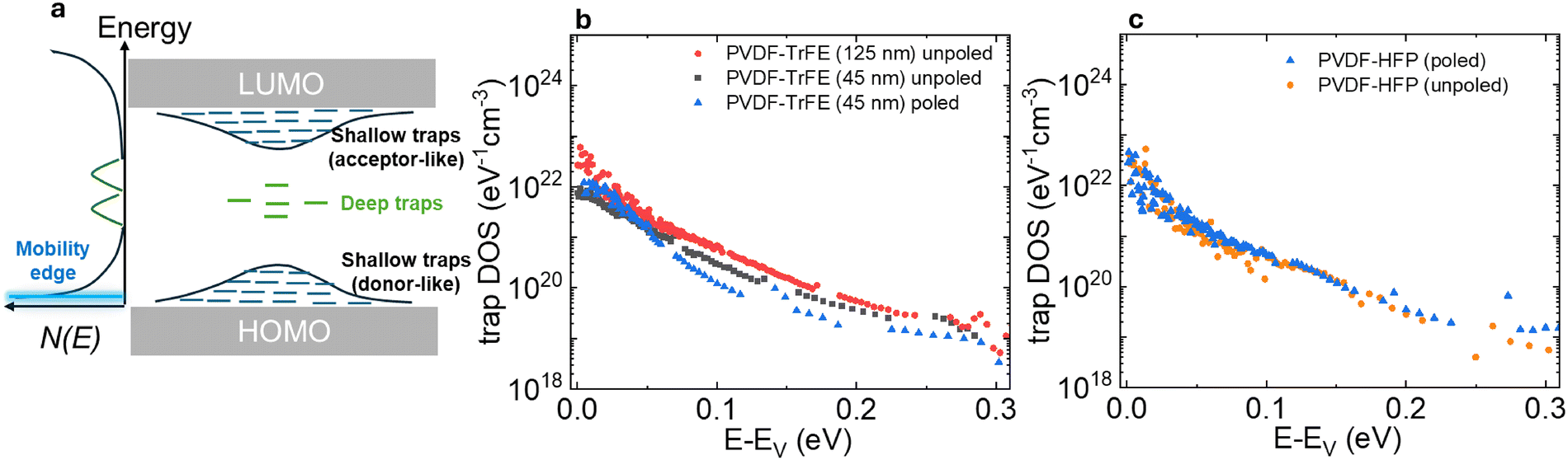 | ||
| Fig. 3 Trap DOS in PVDF-TrFE and PVDF-HFP based DPP-DTT FETs. (a) Schematic DOS (N(E)) and trap states in polymeric semiconductors. Both deep and shallow traps are present. (b) Trap DOS in DPP-DTT FETs for two thicknesses of the PVDF-TrFE layer including a poled layer. (c) Trap DOS in DTT FETs for poled and unpoled PVDF-HFP layers. | ||
The above results demonstrate that vertical poling has a dramatic effect on PVDF-TrFE FETs but not on PVDF-HFP FETs. The improved carrier mobility in poled PVDF-TrFE FET may be rationalized in terms of the lower trap DOS. Our results further suggest that poling does not change the inherent fraction of the crystalline β phase to the α phase; it merely orients the ferroelectric domains. Since the extent of the β phase is much lower in PVDF-HFP compared with PVDF-TrFE, the external poling field has a minimal effect. We next look at the effect of adding ALD grown ultrathin Al2O3 layer to the interface of both PVDF-TrFE and PVDF-HFP devices.
Addition of an ultrathin Al2O3 layer
Al2O3 as a dielectric material has been broadly used in both organic and inorganic transistors. Depending on the growth method of Al2O3, κ can vary between 7–10.1 ALD yields extremely smooth and high-quality films in short cycle times.43 Since the κ values of Al2O3 and PVDF copolymers are almost identical, the addition of Al2O3 serves as an excellent platform to modulate the trap states at the semiconductor–dielectric interface and tune the polarization fluctuation of the polymer ferroelectric without affecting the overall κ of the dielectric stack. With ALD growth temperatures being beyond the Curie temperature of the PVDF copolymers, all films were unpoled. Al2O3 thicknesses between 2 nm and 12 nm were deposited on 45 nm thick PVDF-TrFE or PVDF-HFP prior to the deposition of DPP-DTT. Metal–insulator–metal capacitors were also fabricated, where the overall capacitance/area varied between 94–116 nF cm−2 for 2–12 nm Al2O3 on the PVDF copolymers, respectively.The current–voltage characteristics of PVDF-TrFE and PVDF-HFP based FETs with 5 nm of Al2O3 are compared in Fig. 4. Overall, the PVDF-TrFE FET shows lower carrier mobility and similar SS compared with the unpoled (without Al2O3) devices. Other thicknesses of the Al2O3 layer with PVDF-TrFE also do not improve the FET performance (see ESI†). In contrast, significant improvements in SS and on/off ratio are observed for the PVDF-HFP FET with the 5 nm Al2O3 (Fig. 4(d)). To understand the effect of Al2O3 on PVDF-HFP, we tested several other thicknesses of Al2O3 layer between 2 nm and 12 nm. Current–voltage characteristics of other PVDF-HFP devices with varying Al2O3 are shown in ESI.† In each case we find the SS value to be lower than 300 mV dec−1.
 | ||
| Fig. 4 FET characteristics with 5 nm Al2O3. (a) Device geometry with the addition of Al2O3 layer. (b) and (c) Transfer and output characteristics of a DDP-DTT/PVDF-TrFE FET, respectively. (d) and (e) Transfer and output characteristics of a DDP-DTT/PVDF-HFP FET, respectively. | ||
Adding between 2 nm and 12 nm of Al2O3 on PVDF-HFP has a similar effect on the FET performance, although the carrier mobility decreases slightly for the 12 nm oxide layer. We discuss this reduction in mobility in terms of the contact resistance. The transfer characteristics of four PVDF-HFP FETs with varying Al2O3 thickness between 2 nm to 12 nm are plotted in Fig. 5(a). A histogram of the carrier mobilities and SS for the Al2O3 coated devices are shown in Fig. 5(b) and (c), respectively, for 30–40 devices. A clear reduction in the SS values is observed compared with the non-Al2O3 coated PVDF-HFP FETs. The average value of SS = 400 mV dec−1 for Al2O3 on PVDF-HFP compared with ∼800 mV dec−1 for the non-Al2O3 coated devices (see Fig. S5, ESI†). It should also be pointed out that the average values are from all different thickness of Al2O3, where the 12 nm thickness overall shows a slightly higher value of SS. These data further suggest that the optimum thickness of the Al2O3 layer is between 2 nm and 8 nm for a significant reduction in SS. The transfer curves for the 8 nm Al2O3 device are shown for different values of VDS in Fig. 5(d), and the linear fits for extracting the SS values are shown in Fig. 5(e). The high off current with increasing VDS is expected due to the high shallow trap DOS. At the lowest VDS of −0.7 V, SS = 75 mV dec−1. A similar trend is also seen for the 2 nm Al2O3 on PVDF-HFP FET (see ESI†). This is a clear improvement over the non-Al2O3 coated PVDF-HFP devices which show SS > 300 mV in the linear region (Fig. S6, ESI†). With the addition of a thin Al2O3 layer, we observe some of the lowest values of SS reported for FETs using a polymer semiconductor and a solution processable polymer dielectric.
 | ||
| Fig. 5 Subthreshold characteristics with Al2O3 and PVDF-HFP. (a) Transfer current–voltage characteristics of PVDF-HFP devices with varying thicknesses of Al2O3. (b) Histogram of μsat for PVDF-HFP FETs with Al2O3. (c) Histogram of SS for PVDF-HFP FETs with Al2O3. (d) Transfer current–voltage characteristics for varying values of VDS for the PVDF-HFP FET with 8 nm of Al2O3. (e) Linear fits for obtaining SS for the transfer characteristics shown in (d). | ||
As a quick summary, ALD grown Al2O3 on PVDF-HFP significantly improves SS but slightly reduces the carrier mobility in DPP-DTT FETs. PVDF-TrFE based DPP-DTT FETs, however, show no improvement in SS and there is a further degradation in carrier mobility. Before discussing the differences in SS between the two PVDF systems, we first look at the parameters that govern carrier mobility. The contact resistance of these devices is significant. A comparison of the carrier mobility in the saturation and linear region of a PVDF-HFP FET with 12 nm of Al2O3 as a function of the gate voltage in Fig. 6(a) clearly shows a large difference at higher gate voltages. Ideally, the two mobility curves should overlap. This discrepancy mainly arises due to the contact resistance. The bulk resistance (RBulk) contributes to the contact resistance (RC) due to charge transport within the organic semiconductor, extending from the contact to the channel, as illustrated in Fig. 6(b). Charge carriers move from the source contact to the accumulation layer at the semiconductor–dielectric interface before reaching the drain contact for extraction. Consequently, both metal–semiconductor interface resistance, arising from the resistance associated with the charge-injection barrier, Rint, and RBulk play significant roles in determining RC. Therefore, minimizing RC requires reducing the contributions of both Rint and RBulk.15,44
 | ||
| Fig. 6 Contact resistance in PVDF-HFP FETs. (a) Comparison of the linear and saturation carrier mobilities as a function of the gate voltage in a 12 nm Al2O3 on PVDF-HFP DPP-DTT FET. (b) Schematic of an organic FET showing the origin of contact resistance (RC). Both Rint and RBulk contribute to RC. RC estimation using the transmission line model for (c) PVDF-HFP/DPP-DTT FET and (d) PVDF-HFP/12 nm Al2O3/DPP-DTT FET. The product of the total resistance and width versus channel length for two different gate-source voltages are shown. The intersection of the two straight lines representing the gate biases on the y-axis yields RC. | ||
Using the TLM method as discussed in section: Experimental methods and analysis, we determine RC for a PVDF-HFP FET without Al2O3 and with 12 nm of Al2O3 (Fig. 6(c) and (d)). The contact resistance increases by almost a factor of 14 when 12 nm of Al2O3 is present. Without Al2O3, the contact resistance of the PVDF-HFP FET is approximately 7 kΩ cm. A similar effect is seen for PVDF-TrFE. Adding Al2O3 on PVDF-TrFE also increases RC compared with as-is unpoled PVDF-TrFE FET, which is the main reason why we see a reduction in μsat for Al2O3 on PVDF-TrFE devices. Being top contact devices, adding a barrier layer or self-assembled monolayer for reducing the Schottky barrier, which reduces Rint, is not straightforward. Future direction involving organic ices as negative tone resists45,46 that leave behind thin insulating residues in a modified electron-beam lithography is being developed for deposition under the contacts for reducing Rint in top contact organic FETs.
Next, we discuss the impact of the Al2O3 layer on SS. There is a clear benefit to PVDF-HFP FETs, as seen in Fig. 5, but no significant improvement is observed in PVDF-TrFE FETs. Since the SS values are dictated by the trap states, we look at the trends for both trap DOS as well as the Nint values. Table 1 lists the SS, the normalized SS values, which is the product of SS and Ci, and Nint for DPP-DTT FETs with PVDF-TrFE and PVDF-HFP as the dielectric layer. All FETs have the same L and W values. The SS values noted here are from the transfer characteristics in the saturation region (VDS = −7 V). Lowest normalized SS is seen for the PVDF-HFP FETs with Al2O3, which further indicates low Nit values. Table S1 in ESI† highlights benchmark SS values from other organic FETs in the literature.
| Dielectric | Al2O3 Thickness (nm) | SS (V dec−1) | Normalized SS (nFV dec−1 cm−2) | Nint (cm−2 eV−1) |
|---|---|---|---|---|
| PVDF-TrFE | Unpoled (0) | 1.12 ± 0.05 | 110.8 | 1.11 × 10¹³ |
| Poled (0) | 0.70 ± 0.02 | 69.3 | 6.81 × 10¹² | |
| Al2O3 (2) | 1.31 ± 0.07 | 129.7 | 1.31 × 10¹³ | |
| Al2O3 (3) | 1.45 ± 0.05 | 143.5 | 1.46 × 10¹³ | |
| Al2O3 (5) | 0.98 ± 0.04 | 97 | 9.66 × 10¹² | |
| PVDF-HFP | Unpoled (0) | 0.59 ± 0.02 | 55.4 | 5.27 × 10¹² |
| Poled (0) | 0.67 ± 0.02 | 62.9 | 6.08 × 10¹² | |
| Al2O3 (2) | 0.26 ± 0.01 | 24.4 | 1.99 × 10¹² | |
| Al2O3 (5) | 0.24 ± 0.01 | 22.5 | 1.79 × 10¹² | |
| Al2O3 (8) | 0.29 ± 0.01 | 27.2 | 2.29 × 10¹² | |
| Al2O3 (12) | 0.27 ± 0.01 | 25.3 | 2.09 × 10¹² |
We look more closely into the ALD growth process of Al2O3 on PVDF-TrFE and PVDF-HFP to see how that may affect the two copolymers differently and compare the trap DOS near the HOMO level of the semiconductor with and without Al2O3. A schematic of the first ALD process for the growth of Al2O3 is shown in ESI† (Fig. S10), where the water cycle is followed by TMA, which is then evacuated, followed by re-introduction of water. The morphology of PVDF-TrFE and PVDF-HFP is quite different. The higher fraction of the β phase in PVDF-TrFE enhances its crystallinity compared with PVDF-HFP, which is more amorphous. Moreover, due to the HFP group, PVDF-HFP is more hydrophobic compared with PVDF-TrFE.34 The ALD process typically relies on surface hydroxyl groups to facilitate the reaction. Since both PVDF copolymers lack surface O–H groups, we hypothesize that the reaction of the water pulse in the ALD cycle might induce partial surface modification, generating potential reaction sites for TMA. Further, the first pulse of water may hydroxylate the surface of amorphous PVDF-HFP more than crystalline PVDF-TrFE, allowing oxygen to diffuse. Once TMA reacts on the PVDF-HFP surface and with an additional water cycle, further oxidation may be possible, allowing more oxygen to diffuse. The last stage of the first ALD cycle for the growth of Al2O3 on PVDF-HFP and PVDF-TrFE is shown in Fig. 7(a) and (b), highlighting the diffusion of oxygen in PVDF-HFP.
 | ||
| Fig. 7 ALD growth of Al2O3 on PVDF-HFP and PVDF-TrFE. (a) and (b) The final stage of the first cycle of the ALD process for the deposition of Al2O3 on PVDF-HFP and PVDF-TrFE, respectively. The green domains in PVDF-TrFE represent higher crystallinity. (c) and (d) Trap DOS for PVDF-HFP and PVDF-TrFE FETs, respectively, with and without Al2O3. (e) and (f) Transfer characteristics of representative PVDF-HFP and PVDF-TrFE based FETs, respectively, with and without Al2O3. | ||
HAADF-STEM (high-angle annular dark-field-STEM) images and STEM-EDS (energy dispersive spectroscopy) maps confirm the presence of Al2O3 on PVDF-HFP samples (see Fig. S11, ESI†). While the bulk of the polymer film is similar with and without the Al2O3 layer, details of the interfacial structure are obscured due to holes at either the polymer–oxide (Fig. S11, ESI†) or polymer–electrode (Fig. S12, ESI†) interfaces, depending on sample thickness. These holes result from ion beam damage during the thinning process (Fig. S11, ESI†).
AFM images (included in ESI†) from PVDF-TrFE and PVDF-HFP films coated with 12 nm Al2O3 show some changes in morphology compared with their pristine counterpart. The changes are more significant in PVDF-TrFE where the large ferroelectric domains are somewhat disrupted in the presence of Al2O3.
A surprising result is that the trap DOS, as shown in Fig. 7(c) and (d), with and without Al2O3, are almost identical. This suggests that the shallow trap distribution hardly changes with the deposition of Al2O3. Hence, the improvement in the FET characteristics with Al2O3 on PVDF-HFP arises from a modification of the deep level traps. The transfer curves of representative FETs with and without Al2O3 on PVDF-HFP and PVDF-TrFE are shown in Fig. 7(e) and (f). As discussed earlier, there is hardly any change in SS for PVDF-TrFE FETs with Al2O3. The improved SS with Al2O3 on PVDF-HFP most likely then arises from filling of the interface states with oxygen, which influences the deep level discrete traps (Fig. 3(a)). Such a dependence of the interface states and the deep level states have been observed in other semiconductor–insulator interfaces such as ALD grown Al2O3 and GaN.47 Our results, therefore, warrant other techniques such as deep level transient spectroscopy for a complete picture of the spatial and energy profile of the trap states.48 Such characterization strategies in the future will allow further improvement of organic FETs when modulating the semiconductor–dielectric interface.
It is conceivable that the oxide layer could be replaced with other thin insulating layers as recently demonstrated with negative-tone ethanol-based ice resist49 or a self-assembled monolayer. Such strategies in the future will ensure cost-effective means for fabricating the entire device along with improved performance.
Conclusions
This work demonstrates that external electric field poling remains the most effective approach for reducing polarization fluctuations and enhancing the performance of polymer ferroelectric transistors based on PVDF-TrFE. Further, by reducing the thickness of the PVDF-TrFE film from 125 nm to 45 nm, the operating voltage of the FETs decreases below 8 V. Under optimized conditions, the saturation carrier mobility exceeds 1 cm2 V−1 s−1. In contrast, PVDF-HFP, with lower ferroelectric properties compared with PVDF-TrFE, does not exhibit improved FET properties with external poling.The incorporation of an ultrathin ALD grown Al2O3 interfacial layer plays a critical role in modulating the semiconductor–dielectric interface with PVDF-HFP. SS as low as 75 mV dec−1 in the linear region is observed for PVDF-HFP based FETs with an interfacial Al2O3 layer. No significant improvement in SS or other FET properties are observed with PVDF-TrFE. The differences between the two copolymers arise mainly from their specific morphology. The more amorphous nature of PVDF-HFP compared with PVDF-TrFE allows the penetration of oxygen within the film during the growth of Al2O3, resulting in passivating the interface traps and further influencing the deep level discrete traps in the polymer semiconductor. Our results suggest that Al2O3 treatment could be beneficial for other high κ organic dielectrics where passivation of interface trap states may be required.
Author contributions
A. Ghobadi and S. Guha conceived the work. A. Ghobadi was involved with the fabrication of devices, conducting electrical measurements, and analysing the data. S. Guha was involved with measurements and the analysis of the data. S. Gangopadhyay helped with the analysis and process development for device fabrication. J. Mathai performed ALD growth and helped in the setting up of electrical and AFM measurements. T. Kallaos performed the trap DOS calculations. I. M. Karunarathne, D. M. Gamachchi, and A. C. Meng carried out the lift-off processes and TEM measurements. The manuscript was written by S. Guha and A. Ghobadi with contributions from all authors. All authors have given approval to the final version of the manuscript.Data availability
The data supporting the findings of this study are available within the article and/or have been included as part of its ESI.†Conflicts of interest
There are no conflicts to declare.Acknowledgements
We acknowledge the support of this work through the National Science Foundation (NSF) under Grant No. ECCS-2324839. We thank Evan Restuccia for the Python program for trap DOS calculations.Notes and references
- B. Wang, W. Huang, L. Chi, M. Al-Hashimi, T. J. Marks and A. Facchetti, Chem. Rev., 2018, 118, 5690–5754 CrossRef CAS.
- J. Veres, S. D. Ogier, S. W. Leeming, D. C. Cupertino and S. Mohialdin Khaffaf, Adv. Funct. Mater., 2003, 13, 199–204 CrossRef CAS.
- T. Richards, M. Bird and H. Sirringhaus, J. Chem. Phys., 2008, 128, 234905 CrossRef PubMed.
- H. Chen, W. Zhang, M. Li, G. He and X. Guo, Chem. Rev., 2020, 120, 2879–2949 CrossRef CAS.
- S. P. Senanayak, S. Guha and K. S. Narayan, Phys. Rev. B: Condens. Matter Mater. Phys., 2012, 85, 115311 CrossRef.
- A. Laudari and S. Guha, J. Appl. Phys., 2015, 117, 105501 CrossRef.
- F. Yang, L. Sun, J. Han, B. Li, X. Yu, X. Zhang, X. Ren and W. Hu, ACS Appl. Mater. Interfaces, 2018, 10, 25871–25877 CrossRef CAS.
- T. Wollandt, F. Letzkus, J. N. Burghartz and H. Klauk, Adv. Electron. Mater., 2024, 10, 2300841 CrossRef CAS.
- H. Klauk, U. Zschieschang, J. Pflaum and M. Halik, Nature, 2007, 445, 745–748 CrossRef CAS.
- L. Torsi, A. Dodabalapur, L. J. Rothberg, A. W. P. Fung and H. E. Katz, Science, 1996, 272, 1462–1464 CrossRef CAS PubMed.
- N. F. Mott and E. A. Davis, Electronic processes in non-crystalline materials, Clarendon Press, Oxford University Press, Oxford, New York, 1979 Search PubMed.
- I. N. Hulea, S. Fratini, H. Xie, C. L. Mulder, N. N. Iossad, G. Rastelli, S. Ciuchi and A. F. Morpurgo, Nat. Mater., 2006, 5, 982–986 CrossRef CAS PubMed.
- A. Laudari and S. Guha, J. Appl. Phys., 2019, 125, 035501 CrossRef.
- C. Liu, Y. Xu and Y.-Y. Noh, Mater. Today, 2015, 18, 79–96 CrossRef CAS.
- M. Waldrip, O. D. Jurchescu, D. J. Gundlach and E. G. Bittle, Adv. Funct. Mater., 2020, 30, 1904576 CrossRef CAS.
- J. W. Borchert, B. Peng, F. Letzkus, J. N. Burghartz, P. K. L. Chan, K. Zojer, S. Ludwigs and H. Klauk, Nat. Commun., 2019, 10, 1119 CrossRef PubMed.
- J. Zeng, D. He, J. Qiao, Y. Li, L. Sun, W. Li, J. Xie, S. Gao, L. Pan, P. Wang, Y. Xu, Y. Li, H. Qiu, Y. Shi, J.-B. Xu, W. Ji and X. Wang, Nat. Commun., 2023, 14, 324 CrossRef CAS.
- A. Bilgaiyan, M. Abiko, K. Watanabe and M. Mizukami, ACS Appl. Electron. Mater., 2025, 7, 2583–2592 CrossRef CAS.
- Y. Fu, J. Zhu, Y. Sun, S. Sun, K. Tie, J. Qi, Y. Wang, Z. Wang, Y. Hu, S. Ding, R. Huang, Z. Gong, Y. Huang, X. Chen, L. Li and W. Hu, ACS Nano, 2023, 17, 15044–15052 CrossRef CAS PubMed.
- A. Ghobadi, C. J. Mathai, J. Cook, G. Bian, S. Attar, M. Al-Hashimi, S. Gangopadhyay and S. Guha, Adv. Electron. Mater., 2005, 11, 2400503 CrossRef.
- S. J. Kang, Y. J. Park, I. Bae, K. J. Kim, H.-C. Kim, S. Bauer, E. L. Thomas and C. Park, Adv. Funct. Mater., 2009, 19, 2812–2818 CrossRef CAS.
- S. Das and J. Appenzeller, Nano Lett., 2011, 11, 4003–4007 CrossRef CAS.
- S. K. Hwang, I. Bae, S. M. Cho, R. H. Kim, H. J. Jung and C. Park, Adv. Funct. Mater., 2013, 23, 5484–5493 CrossRef CAS.
- C.-F. Lin, Y.-S. Wu, W.-C. Chen, B.-H. Lin, Y.-C. Lin, C.-C. Kuo and W.-C. Chen, ACS Appl. Electron. Mater., 2025, 7, 1068–1079 CrossRef CAS.
- R. Peng, B. Zhang, G. Dong, Y. Wang, G. Yang, J. Zhang, B. Peng, Y. Zhao and M. Liu, Adv. Funct. Mater., 2024, 34, 2316519 CrossRef CAS.
- L. Lu, W. Ding, J. Liu and B. Yang, Nano Energy, 2020, 78, 105251 CrossRef CAS.
- C. Ribeiro, C. M. Costa, D. M. Correia, J. Nunes-Pereira, J. Oliveira, P. Martins, R. Gonçalves, V. F. Cardoso and S. Lanceros-Méndez, Nat. Protoc., 2018, 13, 681–704 CrossRef CAS PubMed.
- X. Wang, W. Lu, P. Wei, Z. Qin, N. Qiao, X. Qin, M. Zhang, Y. Zhu, L. Bu and G. Lu, ACS Appl. Mater. Interfaces, 2022, 14, 48948–48959 CrossRef CAS PubMed.
- X. Wang, S. Yang, Z. Qin, B. Hu, L. Bu and G. Lu, Adv. Mater., 2023, 35, 2303699 CrossRef CAS PubMed.
- A. J. Lovinger, D. D. Davis, R. E. Cais and J. M. Kometani, Macromolecules, 1986, 19, 1491–1494 CrossRef CAS.
- G. Knotts, A. Bhaumik, K. Ghosh and S. Guha, Appl. Phys. Lett., 2014, 104, 233301 CrossRef.
- R. C. G. Naber, C. Tanase, P. W. M. Blom, G. H. Gelinck, A. W. Marsman, F. J. Touwslager, S. Setayesh and D. M. de Leeuw, Nat. Mater., 2005, 4, 243–248 CrossRef CAS.
- J. Roy, B. Joseph, A. Ashraf K and R. B. Gangineni, Thin Solid Films, 2023, 781, 139981 CrossRef CAS.
- D. M. Correia, J. Nunes-Pereira, D. Alikin, A. L. Kholkin, S. A. C. Carabineiro, L. Rebouta, M. S. Rodrigues, F. Vaz, C. M. Costa and S. Lanceros-Méndez, Polymer, 2019, 169, 138–147 CrossRef CAS.
- E. Restuccia, A. Ghobadi and S. Guha, Adv. Mater. Interfaces, 2025, 2401035 CrossRef.
- A. Ghobadi, S. S. Niavol, E. Restuccia, A. C. Meng and S. Guha, Appl. Phys. Lett., 2024, 124, 153301 CrossRef CAS.
- M. Grünewald, P. Thomas and D. Würtz, Phys. Status Solidi B, 1980, 100, K139–K143 CrossRef.
- W. L. Kalb and B. Batlogg, Phys. Rev. B: Condens. Matter Mater. Phys., 2010, 81, 035327 CrossRef.
- A. Laudari, A. R. Mazza, A. Daykin, S. Khanra, K. Ghosh, F. Cummings, T. Muller, P. F. Miceli and S. Guha, Phys. Rev. Appl., 2018, 10, 014011 CrossRef CAS.
- A. Laudari, A. Pickett, F. Shahedipour-Sandvik, K. Hogan, J. E. Anthony, X. He and S. Guha, Adv. Mater. Interfaces, 2019, 6, 1801787 CrossRef CAS.
- E. H. Nicollian and J. R. Brews, MOS (Metal Oxide Semiconductor) Physics and Technology, Wiley, New York, 2003 Search PubMed.
- M. Yun, S. Gangopadhyay, M. Bai, H. Taub, M. Arif and S. Guha, Org. Electron., 2007, 8, 591–600 CrossRef CAS.
- Y.-S. Min, Y. J. Cho and C. S. Hwang, Chem. Mater., 2005, 17, 626–631 CrossRef CAS.
- P. Darmawan, T. Minari, Y. Xu, S.-L. Li, H. Song, M. Chan and K. Tsukagoshi, Adv. Funct. Mater., 2012, 22, 4577–4583 CrossRef CAS.
- A. Elsukova, A. Han, D. Zhao and M. Beleggia, Nano Lett., 2018, 18, 7576–7582 CrossRef CAS.
- G. Yao, D. Zhao, Y. Hong, S. Wu, D. Liu and M. Qiu, Nanoscale, 2020, 12, 22473–22477 RSC.
- C. M. Jackson, A. R. Arehart, E. Cinkilic, B. McSkimming, J. S. Speck and S. A. Ringel, J. Appl. Phys., 2013, 113, 204505 CrossRef.
- N. M. Johnson, D. J. Bartelink, R. B. Gold and J. F. Gibbons, J. Appl. Phys., 1979, 50, 4828–4833 CrossRef CAS.
- D. A. Chiaro, T. J. Hager, K. T. Renshaw, B. M. Moore, A. Ghobadi, R. I. Haque, A. Han, B. M. Broderick, S. Guha and G. M. King, Nano Lett., 2025, 25, 7107–7114 CrossRef CAS.
Footnote |
| † Electronic supplementary information (ESI) available: Output characteristics of PVDF-TrFE and PVDF-HFP based FETs; histograms of carrier mobilities; current–voltage characteristics of PVDF-TrFE and PVDF-HFP FETs with Al2O3; Dit analysis; subthreshold region transfer characteristics of 2 nm A2O3 with PVDF-HFP; schematic of the ALD process; STEM images and EDS maps; AFM images. See DOI: https://doi.org/10.1039/d5tc01378j |
| This journal is © The Royal Society of Chemistry 2025 |