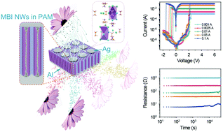
Besides its ubiquitous applications in optoelectronics, halide-perovskites (HPs) have also carved a niche in the domain of resistive switching memories (Re-RAMs). However owing to the material and electrical instability challenges faced by HP thin-films, rarely perovskite Re-RAMs are used to experimentally demonstrate data processing which is a fundamental requirement for neuromorphic applications. Here, for the first time, lead-free, ultrahigh density HP nanowire (NW) array Re-RAM has been utilized to demonstrate image processing via design of convolutional kernels. The devices exhibited superior switching characteristics including a high endurance of 5 × 10⁶ cycles, an ultra-fast erasing and writing speed of 900 ps and 2 ns, respectively, and a retention time >5 × 10⁴ s for the resistances. The work is bolstered by an in-depth mechanistic study and first-principles simulations which provide evidence of electrochemical metallization triggering the switching. Employing the robust multi-level switching behaviour, image processing functions of embossing, outlining and sharpening were successfully implemented.
