 Open Access Article
Creative Commons Attribution 3.0 Unported Licence
New materials for the light-induced hydrogen evolution reaction from the Cu–Si–Ti–O system†
Helge S.
Stein
a,
Ramona
Gutkowski
b,
Alexander
Siegel
a,
Wolfgang
Schuhmann
*bc and
Alfred
Ludwig
*ac
aInstitute for Materials, Ruhr-Universität Bochum, Universitätsstraße 150, 44780 Bochum, Germany. E-mail: alfred.ludwig@rub.de
bAnalytical Chemistry-Center for Electrochemical Sciences (CES), Ruhr-Universität Bochum, Universitätsstr. 150, 44780 Bochum, Germany
cMaterials Research Department, Ruhr-Universität Bochum, Universitätsstr. 150, 44780 Bochum, Germany
First published on 12th January 2016
Abstract
Cu-containing photocathodes are generally limited by fast photocorrosion under working conditions. Hence stabilization of these materials is a key factor in their potential application for the light-induced hydrogen evolution reaction (HER). In order to identify new materials, oxidized Cu–Si–Ti metallic thin film precursor materials libraries were evaluated using a combinatorial approach. High-throughput photoelectrochemical characterization using an automated optical scanning droplet cell was performed on a material library to analyze doping and alloying effects on the light-induced HER. The results revealed that compositions near Ti-doped CuSiO3 (dioptase and copper-polysilicate) and Si-doped Cu3TiOx act as comparatively stable and highly active materials for HER.
Introduction
Photoelectrochemical (PEC) water splitting1 is the scientific endeavor of absorbing sunlight using a semiconductor to drive an electrochemical reaction on its surface to obtain hydrogen as an energy carrier. This work contributes to the ongoing search for new Cu–O-based p-type materials exhibiting promising properties (photovoltage, photocurrent and stability) for solar water splitting. The Cu–Si–Ti–O system was explored for stable absorber materials.2In the materials driven field of photoelectrochemistry, research is directed towards understanding of the fundamental processes in metal oxide photoanodes3 but only a few photocathode materials1 suitable for PEC such as Cu2O (cuprite)4 or CuFeO2![[thin space (1/6-em)]](https://www.rsc.org/images/entities/char_2009.gif) 5 are known. Most of the known metal-oxide photocathode materials are however unstable in aqueous solution2 unless protected by layers of stable materials like TiO2.6 The reason for the low stability of p-type oxides such as cuprite is due to photoreduction of a metal–oxygen bond when hydrogen evolves on the surface. In cuprite this happens as the reduction potential of Cu(II) to Cu(0) lies within the bandgap.7 Most of the well-known p-type metal oxides own their conductivity type to Cu-vacancies as for example in cuprite8 and CuFeO2.5
5 are known. Most of the known metal-oxide photocathode materials are however unstable in aqueous solution2 unless protected by layers of stable materials like TiO2.6 The reason for the low stability of p-type oxides such as cuprite is due to photoreduction of a metal–oxygen bond when hydrogen evolves on the surface. In cuprite this happens as the reduction potential of Cu(II) to Cu(0) lies within the bandgap.7 Most of the well-known p-type metal oxides own their conductivity type to Cu-vacancies as for example in cuprite8 and CuFeO2.5
In this work, new materials are searched for in the Cu–Si–Ti–O system to broaden the choice of p-type absorbers that could be employed in an all oxide tandem solar water splitting device.9,10 The necessary stability enhancement of Cu-containing metal oxides such as cuprite7,11 is investigated by combinatorial alloying with Si and Ti as third elements in an exploratory search for a stable photoabsorber material.
Combinatorial materials science in this work involves combinatorial sputter deposition of gradient thin film materials libraries12,13 and their high-quality and high-throughput in-depth characterization.14,15 Different possibilities have been proposed that enable the deposition of multinary composition spreads like metal nitrate printing,16 evaporation17 or reactive magnetron sputtering.15 Combinatorial optimization of surface protection of cuprite by TiO2 for photovoltaic applications has been suggested,18 but a remaining problem for PEC is the formation of pinholes that drastically reduces the lifetime of a related device.19
The Cu–Si–Ti–O system was chosen, as on the Ti- and Si-rich corners of the quasi-ternary composition space (i.e. the oxygen content is neglected) two well-studied stable oxides exist. However, these materials are either insulators (SiO2) or have a large bandgap20 (TiO2). It has been shown that CuO-based semiconductors can be partially stabilized21 by alloying with Ti. However, the addition of Ti into the lattice is associated with deep donor states that act as non-radiative recombination centers, leading to lower photoactivity as compared to CuO or Cu2O.18,22 These deep donor states give rise to slightly higher optical absorptivity at higher wavelengths assuming a reduced bandgap by e.g. doping or alloying TiO2 with various elements.23 Investigating such effects requires photocurrent spectroscopy at a variety of applied potentials.24
In this work we used combinatorial wedge-type multilayer deposition13 to fabricate simultaneously binary and ternary composition spread type metallic thin film materials libraries in the Cu–Si–Ti system that are subsequently oxidized in air to obtain ternary and quaternary materials in the Cu–Si–Ti–O system. High-throughput PEC characterization of the material libraries was performed to identify stable and highly active materials for HER.
Experimental
Synthesis and pre-characterization of thin film materials libraries
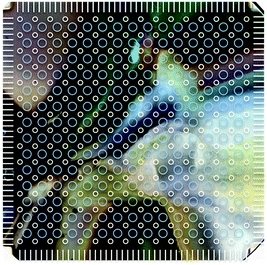
Thin film ternary Cu–Si–Ti composition-spread type materials libraries were deposited in a combinatorial magnetron sputtering system (DCA Finland, CMS 600/400LIN) using a wedge-type deposition method.13,25 The substrate was a polycrystalline Al2O3 on which a 20 nm Au back contact was sputtered prior to the deposition of the materials library. The individual layers of Cu–Si–Ti were sputtered from elemental 4 inch high purity (>99.99%) sputter targets (Lesker). To avoid surface hydroxides, the substrate coated with the Au back contact was annealed for 10 h at 150 °C prior to the Cu–Si–Ti deposition. The total thickness of the as-deposited thin metal precursor films was 300 nm, calculated from measuring individual sputtering rates before the deposition. The compositional spread of the Cu–Si–Ti materials library was analyzed by automated energy dispersive X-ray spectroscopy (Inca-EDX, Oxford Instruments). Subsequently the metallic thin film precursor materials library was oxidized at 600 °C for 8 h in air using a conventional furnace.The measurement areas for the different high-throughput characterization methods are shown in Fig. 1. Around each electrochemical measurement spot four synchrotron X-ray diffraction (XRD) measurements were performed.
Synchrotron diffraction
Wide-angle synchrotron XRD was carried out at BL9 at the DELTA Synchrotron (Technical University Dortmund). The experimental details and setup of the diffraction experiment can be found elsewhere.26 The X-ray spot is about 1–2 mm2 in diameter. The X-ray detector was a 2D MAR345 (marXperts). The X-ray energy was 20 keV. XRD patterns on the 15 × 15 grid were recorded by mounting the sample on a computer-controlled five-axis stage. For phase analysis the 2D patterns were integrated. Background subtraction was performed according to the algorithm by Sonneveld & Visser.27Fig. 1 shows the real space coordinates of each XRD measurement area. Phase region analysis was aided by machine learning algorithms on XRD patterns by using the approach of clustering similar XRD pattern by their geometric distance as described elsewhere.28Photoelectrochemistry
Photoelectrochemistry (PEC) measurements were performed by means of an automated scanning droplet cell14 with circular measurement areas of 1 mm diameter on a 16 × 16 grid as shown in Fig. 1. Prior to each measurement the open circuit potential (OCP) was determined first in the dark and then under illumination. A positive shift in open circuit potential (ΔOCP) is expected for a p-type material.29 It was shown previously that the OCP and its shift correlate with the occurrence of different phases.24PEC measurements were performed in a three electrode set-up with a Ag/AgCl/3 M KCl (210 mV vs. NHE) as reference electrode and a Pt wire as counter electrode in 0.1 M KH2PO4 at pH 7. The applied potential (Eappl) was calculated against the reversible hydrogen electrode (RHE) for better comparability: ERHE = 210 mV + Eappl + (59 mV × pH). The linear sweep was started at 923 mV (vs. RHE) with a negative slope to −50 mV at a scan rate of 1 mV s−1. A 150 W Xe-Lamp (Hamamatsu) was used as light source and the power of the incident light was around 100 mW cm−2. The lamp shutter was opened and closed for 5 s each.
Results and discussion
High-throughput XRD for combinatorial phase mapping
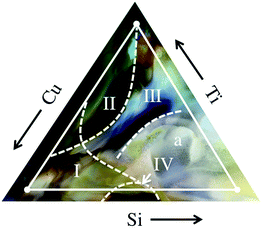
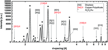
By utilizing machine learning algorithms on XRD patterns obtained from gracing-incidence synchrotron measurements,28 four major phase regions were identified in the Cu–Si–Ti–O materials library, marked by Roman numerals in Fig. 2. These regions exhibit a good correlation between changes in color and phase boundaries as shown by the RGB background image in Fig. 2. Region I denotes a mixed phase consisting of CuO and Cu2O and probably X-ray amorphous Si–Ti–O. Region II comprises the Cu–Ti–O quasi-binary phase in which several mixed phases (Cu2O, CuO, TiOx, Cu1−xTixOy) exist. Region III consists of X-ray amorphous Ti-rich Ti–Cu–Si–O and off-stoichiometric SiTiOx phases. The phase region IV near a nominal composition of Cu50Si50Ox (discussed in detail later), is identified to be a mixture of dioptase and copper-polysilicate.Fig. 3 shows a representative XRD pattern of phase region IV with all peaks marked. There is no indication of a solid solution or a mixture of any of the other possible phases like CuO, Cu2O, SiO2 as no diffraction peaks of these structures are visible. Only the diffraction peak of copper-polysilicate [130] at d = 2.4516 Å overlaps with the [111] peaks of Cu2O and CuO. No further peaks are visible in the diffraction pattern. We conclude that around Ti:Cu50Si50Ox a quasi-binary compound exists that is alloyed with Ti. This is in agreement with the thermodynamic results by Kiseleva et al.33 who report an enthalpy of formation of −42.2 kJ mol−1 for dioptase from CuO (tenorite) and SiO2 (quartz).
The bright white color in the Si–O rich side of Fig. 2 may indicate a detached film as no metal color (Au back contact) is visible.
Photoelectrochemical characterization
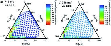
Visualization of the multidimensional dataset of linear sweeps voltammograms under chopped light illumination over the ternary composition spread is shown by color coding a ternary diagram with the photocurrent densities at two potentials as shown in Fig. 4. The photocurrent is calculated as the difference between the current density under illumination and in the dark after equilibration.The potential of 0.716 V vs. RHE at which the photocurrents are plotted in Fig. 4a was chosen as reference as it roughly corresponds to the photocurrent onset potential of the materials. The potential of 0.316 V vs. RHE in Fig. 4b is the potential at which the highest photocurrent density was observed. Apparently only regions at quasi-binary compositions of Cu–Ti–O and Cu–Si–O with Cu >50 at% and the fourth element (Si or Ti) <20 at% are photoactive.
In the following sections, these two regions are discussed as quasi-binary. For Ti–O and Si–O rich compositions, no photocurrents were observed which is attributed to a too large band gap for significant visible light absorption. The Cu-rich corner of the quasi-binary Cu–Ti–O composition space at the left side of the ternary diagram in Fig. 4a and b shows highest photocurrent densities of up to −420 μA cm−2 at 0.316 V vs. RHE at high Cu concentrations of around 70 at%, Ti contents <30 at%, and Si contents <20 at%. Deviations from these apparently optimal compositions result in significantly lower photocurrent densities. Especially the incorporation of Si into the Cu–Ti–O compositions results in a decay of photoactivity.
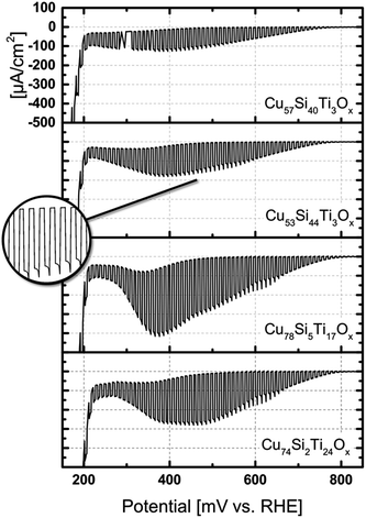
In the Cu–Si–O quasi-binary subsystem photocurrents are comparably low but the photocurrent onset potentials remain at around 0.716–0.800 V vs. RHE. At the composition close to Cu50Si50Ox (Cu55Si44Ti3Ox and Cu57Si40Ti3Ox) highest photocurrent densities of up to −200 μA cm−2 at about 0.4 V vs. RHE are obtained as shown in the top of Fig. 5.
Fig. 5 shows linear sweep voltammograms under chopped light illumination for four selected measurement areas representing the two most active compositions from the Cu–Si–O and Cu–Ti–O quasi-binary subsystems shown in Fig. 4.
The dark current for Cu-rich samples (Cu >60 at%) started to increase at 500 mV vs. RHE significantly, indicating lower stability as compared to Cu57Si40Ti3Ox most likely due to the reduction of Cu2+ ions (peak at 350 mV vs. RHE). For Cu57Si40Ti3Ox no reduction peak was observed at this potential suggesting that in Cu57Si40Ti3Ox copper is stabilized, although the photocurrent is significantly smaller as compared to Cu-rich phases (Cu >60%). However, optimization of the layer thickness, nanostructuring or decoration by co-catalyst materials for the hydrogen evolution reaction (HER) may improve the photoelectrochemical performance. Comparing this material composition to previously described highly crystalline Cu2O,32 the reduction peak of copper shifted by about 200 mV to anodic potentials suggesting mixed oxidation states. To further illustrate the enhancement of the stability of quasi-binary Cu–Si–O and Cu–Ti–O in Cu55Si44Ti3Ox and Cu57Si40Ti3Ox linear sweep voltammograms under chopped light illumination of material compositions with a Cu-content varying between 23% and 88% were recorded (Fig. S1 and S2 ESI†). For both quasi-binary systems especially at high Cu concentration and low concentrations of Ti or Si, respectively, the dark current increased rapidly with increasing bias potential. The stability could be improved by decreasing the Cu-content or increasing the Ti or Si content, respectively. However, Cu reduction peaks are observed at Ti <20%. Comparing both quasi-binary material compositions, the addition of Si leads to more stable films than the addition of Ti.
The photocurrent densities at applied potentials >0.650 V vs. RHE as well as the photocurrent onset potential is essentially the same for all selected measurement areas. All samples depicted in Fig. 5 show small overshoots within the 5 s measurement time under illumination (inset in Fig. 5), associated to low surface recombination of photogenerated charge carriers. The current increase at potentials <0.2 V vs. RHE was attributed to gas evolution.
Conclusions
Two new photocathode materials with compositions close to Si:Cu75Ti25Ox and Ti:Cu50Si50Ox were identified as light absorber materials with promising photocurrent densities and onset potentials on a combinatorial materials library analyzed by high-throughput methods. Both identified materials are p-type semiconductors that show slightly enhanced stability over Cu2O11 and CuO due to comparably lower dark currents at potentials that match the reduction of Cu-cations. The two identified materials show promising photovoltages. Dioptase may contain crystal water in the narrow hollow Si6O18 silicate rings, affecting its electronic properties.30 Dioptase is assumed to be a promising material for further studies, as the comparably large hollow silicate rings might show catalytic31 properties as here solely Si–O bonds are exposed to the electrolyte. Due to its complex crystal and electronic structure dioptase could be used as base material for the optimization of photocathodes by introducing additional dopants (e.g. Zr, Hf, Zn, Al, Nb). As dioptase as well as Cu-polysilicate consist of transition metal oxides with partially filled d-states classical DFT methods like PBE fail to conclusively address accurately the electronic structure of the semiconductor and suggest metallic behavior.30 Therefore more accurate (i.e. DFT+U) calculations are needed to gain a deeper understanding of the material especially for optimization through doping.Acknowledgements
The authors are grateful to the DFG for the financial support within the SPP1613 (LU1175/10-1, LU1175/10-2, Schu929/12-1, Schu929/12-2). H. S. S. acknowledges a PhD fellowship from the International Max Planck Research School for Surface and Interface Engineering (IMPRS-SurMat).Notes and References
- M. G. Walter, E. L. Warren, J. R. McKone, S. W. Boettcher, Q. Mi, E. A. Santori and N. S. Lewis, Chem. Rev., 2010, 110, 6446–6473 CrossRef CAS PubMed
.
- P. E. de Jongh, D. Vanmaekelbergh and J. J. Kelly, Chem. Commun., 1999, 1069–1070 RSC
.
- A. Fujishima and K. Honda, Nature, 1972, 238, 37–38 CrossRef CAS PubMed
.
- A. Paracchino, V. Laporte, K. Sivula, M. Grätzel and E. Thimsen, Nat. Mater., 2011, 10, 456–461 CrossRef CAS PubMed
.
- C. G. Read, Y. Park and K.-S. Choi, J. Phys. Chem. Lett., 2012, 3, 1872–1876 CrossRef CAS PubMed
.
-
M. Pourbaix, Atlas d'Equilibres Electrochimiques, Gauthier-Villars, Paris, 1963 Search PubMed
.
- P. E. de Jongh, D. Vanmaekelbergh and J. J. Kelly, Chem. Commun., 1999, 1069–1070 RSC
.
- B. K. Meyer, A. Polity, D. Reppin, M. Becker, P. Hering, P. J. Klar, T. Sander, C. Reindl, J. Benz, M. Eickhoff, C. Heiliger, M. Heinemann, J. Bläsing, A. Krost, S. Shokovets, C. Müller and C. Ronning, Phys. Status Solidi B, 2012, 249, 1487–1509 CrossRef CAS
.
- C. X. Kronawitter, L. Vayssieres, S. Shen, L. Guo, D. A. Wheeler, J. Z. Zhang, B. R. Antoun and S. S. Mao, Energy Environ. Sci., 2011, 4, 3889–3911 CAS
.
- S. Hu, C. Xiang, S. Haussener, A. D. Berger and N. S. Lewis, Energy Environ. Sci., 2013, 6, 2984 CAS
.
- H. Stein, D. Naujoks, D. Grochla, C. Khare, R. Gutkowski, S. Grützke, W. Schuhmann and A. Ludwig, Phys. Status Solidi A, 2015, 212, 2798–2804 CrossRef CAS
.
- M. L. Green, I. Takeuchi and J. R. Hattrick-Simpers, J. Appl. Phys., 2013, 113, 231101–231154 CrossRef
.
- A. Ludwig, R. Zarnetta, S. Hamann, A. Savan and S. Thienhaus, Int. J. Mater. Res., 2013, 99, 1144–1149 CrossRef
.
- K. Sliozberg, D. Schäfer, T. Erichsen, R. Meyer, C. Khare, A. Ludwig and W. Schuhmann, ChemSusChem, 2015, 8, 1270–1278 CrossRef CAS PubMed
.
- R. Meyer, K. Sliozberg, C. Khare, W. Schuhmann and A. Ludwig, ChemSusChem, 2015, 8, 1279–1285 CrossRef CAS PubMed
.
- M. Woodhouse, G. S. Herman and B. A. Parkinson, Chem. Mater., 2005, 17, 4318–4324 CrossRef CAS
.
- J. P. Kollender, A. I. Mardare and A. W. Hassel, J. Electrochem. Soc., 2015, 162, H187–H193 CrossRef CAS
.
- M. Pavan, S. Rühle, A. Ginsburg, D. A. Keller, H.-N. Barad, P. M. Sberna, D. Nunes, R. Martins, A. Y. Anderson, A. Zaban and E. Fortunato, Sol. Energy Mater. Sol. Cells, 2015, 132, 549–556 CrossRef CAS
.
- B. Parkinson, Acc. Chem. Res., 1984, 17, 431–437 CrossRef CAS
.
- V. N. Bogomolov and D. N. Mirlin, Phys. Status Solidi B, 1968, 27, 443–453 CrossRef CAS
.
- H. Tang, M. A. Matin, H. Wang, S. Sudhakar, L. Chen, M. M. Al-Jassim and Y. Yan, J. Electron. Mater., 2012, 41, 3062–3067 CrossRef
.
- A. Paracchino, V. Laporte, K. Sivula, M. Grätzel and E. Thimsen, Nat. Mater., 2011, 10, 456–461 CrossRef CAS PubMed
.
- H. S. Park, D. H. Kim, S. J. Kim and K. S. Lee, J. Alloys Compd., 2006, 415, 51–55 CrossRef CAS
.
- K. Sliozberg, H. S. Stein, C. Khare, B. A. Parkinson, A. Ludwig and W. Schuhmann, ACS Appl. Mater. Interfaces, 2015, 7, 4883–4889 CAS
.
- R. Zarnetta, R. Takahashi, M. L. Young, A. Savan, Y. Furuya, S. Thienhaus, B. Maaß, M. Rahim, J. Frenzel, H. Brunken, Y. S. Chu, V. Srivastava, R. D. James, I. Takeuchi, G. Eggeler and A. Ludwig, Adv. Funct. Mater., 2010, 20, 1917–1923 CrossRef CAS
.
- C. Krywka, M. Paulus, C. Sternemann, M. Volmer, A. Remhof, G. Nowak, A. Nefedov, B. Poter, M. Spiegel and M. Tolan, J. Synchrotron Radiat., 2005, 13(8–13), 1–6 Search PubMed
.
- E. J. Sonneveld and J. W. Visser, J. Appl. Crystallogr., 1975, 8, 1–7 CrossRef
.
- C. J. Long, D. Bunker, X. Li, V. L. Karen and I. Takeuchi, Rev. Sci. Instrum., 2009, 80, 103902–103906 CrossRef CAS PubMed
.
-
Z. Chen, T. G. Deutsch, H. N. Dinh, K. Domen, K. Emery, A. J. Forman, N. Gaillard, R. Garland, C. Heske, T. F. Jaramillo, A. Kleiman-Shwarsctein, E. Miller, K. Takanabe and J. Turner, in Photoelectrochemical Water Splitting, Springer New York, New York, NY, 2013, pp. 63–85 Search PubMed
.
- O. Janson, A. A. Tsirlin, M. Schmitt and H. Rosner, Phys. Rev. B: Condens. Matter Mater. Phys., 2010, 82, 014424–014428 CrossRef
.
- S. Raabe, D. Mierwaldt, J. Ciston, M. Uijttewaal, H. Stein, J. Hoffmann, Y. Zhu, P. Blöchl and C. Jooss, Adv. Funct. Mater., 2012, 22, 3378–3388 CrossRef CAS
.
- R. E. Newman and R. P. Santoro, Phys. Status Solidi, 1967, 19, K87 CrossRef
.
- I. A. Kiseleva, L. P. Ogorodova, L. V. Melchakova and M. R. Bisengalieva, J. Chem. Thermodyn., 1993, 25, 621–630 CrossRef CAS
.
Footnote |
| † Electronic supplementary information (ESI) available. See DOI: 10.1039/c5ta10186g |
| This journal is © The Royal Society of Chemistry 2016 |

